KR20180098481A - 집적 회로 패터닝 방법 - Google Patents
집적 회로 패터닝 방법 Download PDFInfo
- Publication number
- KR20180098481A KR20180098481A KR1020180095457A KR20180095457A KR20180098481A KR 20180098481 A KR20180098481 A KR 20180098481A KR 1020180095457 A KR1020180095457 A KR 1020180095457A KR 20180095457 A KR20180095457 A KR 20180095457A KR 20180098481 A KR20180098481 A KR 20180098481A
- Authority
- KR
- South Korea
- Prior art keywords
- lines
- substrate
- features
- spacer
- spacer layer
- Prior art date
- Legal status (The legal status is an assumption and is not a legal conclusion. Google has not performed a legal analysis and makes no representation as to the accuracy of the status listed.)
- Granted
Links
Images


Classifications
-
- H—ELECTRICITY
- H10—SEMICONDUCTOR DEVICES; ELECTRIC SOLID-STATE DEVICES NOT OTHERWISE PROVIDED FOR
- H10P—GENERIC PROCESSES OR APPARATUS FOR THE MANUFACTURE OR TREATMENT OF DEVICES COVERED BY CLASS H10
- H10P76/00—Manufacture or treatment of masks on semiconductor bodies, e.g. by lithography or photolithography
- H10P76/20—Manufacture or treatment of masks on semiconductor bodies, e.g. by lithography or photolithography of masks comprising organic materials
- H10P76/204—Manufacture or treatment of masks on semiconductor bodies, e.g. by lithography or photolithography of masks comprising organic materials of organic photoresist masks
- H10P76/2041—Photolithographic processes
-
- H01L21/0274—
-
- H—ELECTRICITY
- H10—SEMICONDUCTOR DEVICES; ELECTRIC SOLID-STATE DEVICES NOT OTHERWISE PROVIDED FOR
- H10P—GENERIC PROCESSES OR APPARATUS FOR THE MANUFACTURE OR TREATMENT OF DEVICES COVERED BY CLASS H10
- H10P76/00—Manufacture or treatment of masks on semiconductor bodies, e.g. by lithography or photolithography
- H10P76/40—Manufacture or treatment of masks on semiconductor bodies, e.g. by lithography or photolithography of masks comprising inorganic materials
- H10P76/408—Manufacture or treatment of masks on semiconductor bodies, e.g. by lithography or photolithography of masks comprising inorganic materials characterised by their sizes, orientations, dispositions, behaviours or shapes
- H10P76/4088—Processes for improving the resolution of the masks
-
- C—CHEMISTRY; METALLURGY
- C23—COATING METALLIC MATERIAL; COATING MATERIAL WITH METALLIC MATERIAL; CHEMICAL SURFACE TREATMENT; DIFFUSION TREATMENT OF METALLIC MATERIAL; COATING BY VACUUM EVAPORATION, BY SPUTTERING, BY ION IMPLANTATION OR BY CHEMICAL VAPOUR DEPOSITION, IN GENERAL; INHIBITING CORROSION OF METALLIC MATERIAL OR INCRUSTATION IN GENERAL
- C23G—CLEANING OR DE-GREASING OF METALLIC MATERIAL BY CHEMICAL METHODS OTHER THAN ELECTROLYSIS
- C23G1/00—Cleaning or pickling metallic material with solutions or molten salts
- C23G1/02—Cleaning or pickling metallic material with solutions or molten salts with acid solutions
-
- H01L21/0332—
-
- H—ELECTRICITY
- H10—SEMICONDUCTOR DEVICES; ELECTRIC SOLID-STATE DEVICES NOT OTHERWISE PROVIDED FOR
- H10P—GENERIC PROCESSES OR APPARATUS FOR THE MANUFACTURE OR TREATMENT OF DEVICES COVERED BY CLASS H10
- H10P50/00—Etching of wafers, substrates or parts of devices
- H10P50/69—Etching of wafers, substrates or parts of devices using masks for semiconductor materials
- H10P50/691—Etching of wafers, substrates or parts of devices using masks for semiconductor materials for Group V materials or Group III-V materials
- H10P50/693—Etching of wafers, substrates or parts of devices using masks for semiconductor materials for Group V materials or Group III-V materials characterised by their size, orientation, disposition, behaviour or shape, in horizontal or vertical plane
- H10P50/695—Etching of wafers, substrates or parts of devices using masks for semiconductor materials for Group V materials or Group III-V materials characterised by their size, orientation, disposition, behaviour or shape, in horizontal or vertical plane characterised by the process involved to create the mask, e.g. lift-off masks or sidewalls or to modify the mask
-
- H—ELECTRICITY
- H10—SEMICONDUCTOR DEVICES; ELECTRIC SOLID-STATE DEVICES NOT OTHERWISE PROVIDED FOR
- H10P—GENERIC PROCESSES OR APPARATUS FOR THE MANUFACTURE OR TREATMENT OF DEVICES COVERED BY CLASS H10
- H10P50/00—Etching of wafers, substrates or parts of devices
- H10P50/73—Etching of wafers, substrates or parts of devices using masks for insulating materials
-
- H—ELECTRICITY
- H10—SEMICONDUCTOR DEVICES; ELECTRIC SOLID-STATE DEVICES NOT OTHERWISE PROVIDED FOR
- H10P—GENERIC PROCESSES OR APPARATUS FOR THE MANUFACTURE OR TREATMENT OF DEVICES COVERED BY CLASS H10
- H10P76/00—Manufacture or treatment of masks on semiconductor bodies, e.g. by lithography or photolithography
- H10P76/40—Manufacture or treatment of masks on semiconductor bodies, e.g. by lithography or photolithography of masks comprising inorganic materials
- H10P76/405—Manufacture or treatment of masks on semiconductor bodies, e.g. by lithography or photolithography of masks comprising inorganic materials characterised by their composition, e.g. multilayer masks
-
- H—ELECTRICITY
- H10—SEMICONDUCTOR DEVICES; ELECTRIC SOLID-STATE DEVICES NOT OTHERWISE PROVIDED FOR
- H10P—GENERIC PROCESSES OR APPARATUS FOR THE MANUFACTURE OR TREATMENT OF DEVICES COVERED BY CLASS H10
- H10P76/00—Manufacture or treatment of masks on semiconductor bodies, e.g. by lithography or photolithography
- H10P76/40—Manufacture or treatment of masks on semiconductor bodies, e.g. by lithography or photolithography of masks comprising inorganic materials
- H10P76/408—Manufacture or treatment of masks on semiconductor bodies, e.g. by lithography or photolithography of masks comprising inorganic materials characterised by their sizes, orientations, dispositions, behaviours or shapes
- H10P76/4085—Manufacture or treatment of masks on semiconductor bodies, e.g. by lithography or photolithography of masks comprising inorganic materials characterised by their sizes, orientations, dispositions, behaviours or shapes characterised by the processes involved to create the masks
-
- H—ELECTRICITY
- H10—SEMICONDUCTOR DEVICES; ELECTRIC SOLID-STATE DEVICES NOT OTHERWISE PROVIDED FOR
- H10P—GENERIC PROCESSES OR APPARATUS FOR THE MANUFACTURE OR TREATMENT OF DEVICES COVERED BY CLASS H10
- H10P50/00—Etching of wafers, substrates or parts of devices
- H10P50/20—Dry etching; Plasma etching; Reactive-ion etching
- H10P50/28—Dry etching; Plasma etching; Reactive-ion etching of insulating materials
- H10P50/282—Dry etching; Plasma etching; Reactive-ion etching of insulating materials of inorganic materials
- H10P50/283—Dry etching; Plasma etching; Reactive-ion etching of insulating materials of inorganic materials by chemical means
-
- H—ELECTRICITY
- H10—SEMICONDUCTOR DEVICES; ELECTRIC SOLID-STATE DEVICES NOT OTHERWISE PROVIDED FOR
- H10P—GENERIC PROCESSES OR APPARATUS FOR THE MANUFACTURE OR TREATMENT OF DEVICES COVERED BY CLASS H10
- H10P50/00—Etching of wafers, substrates or parts of devices
- H10P50/60—Wet etching
- H10P50/66—Wet etching of conductive or resistive materials
- H10P50/663—Wet etching of conductive or resistive materials by chemical means only
- H10P50/667—Wet etching of conductive or resistive materials by chemical means only by liquid etching only
Landscapes
- Chemical & Material Sciences (AREA)
- Chemical Kinetics & Catalysis (AREA)
- General Chemical & Material Sciences (AREA)
- Engineering & Computer Science (AREA)
- Materials Engineering (AREA)
- Mechanical Engineering (AREA)
- Metallurgy (AREA)
- Organic Chemistry (AREA)
- Internal Circuitry In Semiconductor Integrated Circuit Devices (AREA)
Abstract
Description
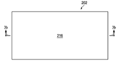
도 2는 본 발명의 다양한 양태에 따른 예시적인 기판 및 기판 상부에 형성된 목표 패턴을 도시하는 도면.
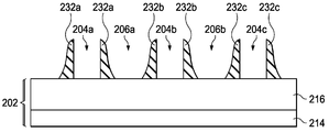
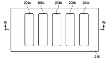
도 3a 내지 도 9b는 본 발명의 실시예에 따른 도 1의 방법에 따라 도 2의 목표 패턴을 형성하는 방법의 상면도 및 단면도.
202 : 기판
218a, 218b, 218c : 맨드릴 라인
216 : 재료 층
220 : 스페이서 층
Claims (9)
- 집적 회로를 위한 목표 패턴을 형성하는 방법에 있어서,
제1 마스크를 이용하여 복수의 라인들을 기판 위에 형성하는 단계;
상기 기판 위에, 복수의 라인들 위에 그리고 복수의 라인들의 측벽들 상에 스페이서 층을 형성하는 단계;
상기 복수의 라인들의 상면과 상기 기판의 일부를 노출시키기 위해 건식 에칭 공정을 이용하여 상기 스페이서 층의 적어도 일부를 제거하는 단계로서, 상기 복수의 라인들의 측벽들 상에 스페이서 특징부들을 형성하고, 상기 스페이서 특징부들 사이에 그리고 상기 기판 상에 트렌치들이 형성되는, 상기 스페이서 층의 적어도 일부를 제거하는 단계;
상기 스페이서 층의 적어도 일부를 제거하는 단계 이후에, 상기 트렌치들의 폭이 상기 복수의 라인들의 폭과 동일해지도록 상기 복수의 라인들의 측벽들 상의 상기 스페이서 특징부들을 수축시키는 단계로서, 상기 스페이서 특징부들의 수축은 등방성이며, 상기 복수의 라인들과 상기 기판은 변경되지 않으면서 상기 스페이서 특징부들의 일부를 제거하기 위해 선택적으로 조정되는(tuned) 세정 용액을 이용하는 습식 세정 공정을 포함하는 것인, 상기 스페이서 특징부들을 수축시키는 단계; 및
상기 스페이서 특징부들을 수축시킨 후에, 상기 복수의 라인들을 제거함으로써 패터닝된 스페이서 층을 기판 위에 제공하는 단계
를 포함하는 집적 회로를 위한 목표 패턴 형성 방법. - 제1항에 있어서,
적어도 상기 패터닝된 스페이서 층을 에칭 마스크로서 이용하여 상기 기판을 에칭하는 단계; 및
상기 에칭 후에 상기 패터닝된 스페이서 층을 제거하는 단계를 더 포함하는 집적 회로를 위한 목표 패턴 형성 방법. - 제1항에 있어서,
상기 복수의 라인들을 형성하는 단계는,
상기 기판 위에 레지스트 층을 형성하는 단계; 및
상기 제1 마스크를 이용하여 상기 레지스트 층을 패터닝하는 단계를 포함하는 것인, 집적 회로를 위한 목표 패턴 형성 방법. - 제1항에 있어서,
상기 건식 에칭 공정은 이방성 에칭 공정을 포함하는 것인, 집적 회로를 위한 목표 패턴 형성 방법. - 제1항에 있어서,
상기 스페이서 층은 티타늄 질화물 또는 티타늄 산화물을 포함하고,
상기 습식 세정 공정은 플루오르화 수소산(HF) 또는 SCl 용액을 이용하는 것인, 집적 회로를 위한 목표 패턴 형성 방법. - 제1항에 있어서,
상기 스페이서 층은 실리콘 질화물을 포함하고,
상기 습식 세정 공정은 플루오르화 수소산(HF) 또는 인산(H2PO4 -)을 이용하는 것인, 집적 회로를 위한 목표 패턴 형성 방법. - 제1항에 있어서,
상기 스페이서 층을 형성하기 전에 상기 복수의 라인들을 트리밍하는 단계를 더 포함하는, 집적 회로를 위한 목표 패턴 형성 방법. - 집적 회로를 위한 목표 패턴을 형성하는 방법에 있어서,
제1 마스크를 이용하여 기판을 패터닝함으로써 제1의 복수의 특징부들을 형성하는 단계;
상기 기판 위에, 상기 제1의 복수의 특징부들들 위에, 그리고 상기 제1의 복수의 특징부들의 측벽들 상에 스페이서 층을 형성하는 단계;
상기 제1의 복수의 특징부들의 상면과 상기 기판의 일부를 노출시키기 위해 상기 스페이서 층의 적어도 일부에 대해 건식 에칭 공정을 수행하는 단계로서, 상기 제1의 복수의 특징부들의 측벽들 상에 스페이서 특징부들을 형성하고, 상기 스페이서 특징부들 사이에 그리고 상기 기판 상에 트렌치들이 형성되는, 상기 건식 에칭 공정을 수행하는 단계;
상기 스페이서 층의 적어도 일부에 대해 건식 에칭 공정을 수행하는 단계 이후에, 상기 트렌치들의 폭이 상기 제1의 복수의 특징부들의 폭과 동일해지도록, 상기 제1의 복수의 특징부들과 상기 기판이 변경되지 않게 유지하면서 상기 스페이서 특징부들의 두께를 등방성으로 감소시키기 위해 상기 스페이서 특징부들에 대해 선택적으로 조정되는(tuned) 세정 용액을 이용하는 습식 세정 공정을 수행하는 단계; 및
상기 습식 세정 공정을 수행한 후에, 상기 제1 복수의 특징부들을 제거하는 단계
를 포함하는 집적 회로를 위한 목표 패턴 형성 방법. - 집적 회로를 위한 목표 패턴을 형성하는 방법에 있어서,
제1 방향으로 제1 치수를 갖는 2개의 라인을 포토리소그래피 공정을 이용하여 기판 위에 형성하는 단계;
상기 기판 위에, 상기 2개의 라인 위에 그리고 상기 2개의 라인의 측벽들 상에 제1 재료를 성막하는 단계;
상기 2개의 라인의 상면과 상기 기판의 일부를 노출시키기 위해 상기 제1 재료에 대해 건식 에칭 공정을 수행하는 단계;
상기 제1 재료에 대해 건신 에칭 공정을 수행하는 단계 이후에, 상기 2개의 라인과 상기 기판은 변경되지 않으면서, 상기 2개의 라인의 측벽들 상에 배치된 상기 제1 재료가 상기 제1 방향으로 제2 치수만큼 이격되도록 상기 제1 재료의 두께를 등방성으로 감소시키기 위해 상기 제1 재료에 대해 선택적으로 조정되는(tuned) 세정 용액을 이용하는 습식 세정 공정을 수행하는 단계로서, 상기 2개의 라인들 사이에서 상기 제2 치수를 갖는 상기 제1 재료 간의 거리가 상기 2개의 라인들의 상기 제1 치수와 동일한 것인, 상기 습식 세정 공정을 수행하는 단계; 및
상기 습식 세정 공정을 수행한 후에, 상기 2개의 라인을 제거하는 단계를 포함하는 집적 회로를 위한 목표 패턴 형성 방법.
Applications Claiming Priority (2)
| Application Number | Priority Date | Filing Date | Title |
|---|---|---|---|
| US14/088,569 US9129814B2 (en) | 2013-11-25 | 2013-11-25 | Method for integrated circuit patterning |
| US14/088,569 | 2013-11-25 |
Related Parent Applications (1)
| Application Number | Title | Priority Date | Filing Date |
|---|---|---|---|
| KR1020170052439A Division KR20170047205A (ko) | 2013-11-25 | 2017-04-24 | 집적 회로 패터닝 방법 |
Publications (2)
| Publication Number | Publication Date |
|---|---|
| KR20180098481A true KR20180098481A (ko) | 2018-09-04 |
| KR102010188B1 KR102010188B1 (ko) | 2019-08-12 |
Family
ID=53183021
Family Applications (3)
| Application Number | Title | Priority Date | Filing Date |
|---|---|---|---|
| KR1020140165116A Ceased KR20150060577A (ko) | 2013-11-25 | 2014-11-25 | 집적 회로 패터닝 방법 |
| KR1020170052439A Ceased KR20170047205A (ko) | 2013-11-25 | 2017-04-24 | 집적 회로 패터닝 방법 |
| KR1020180095457A Active KR102010188B1 (ko) | 2013-11-25 | 2018-08-16 | 집적 회로 패터닝 방법 |
Family Applications Before (2)
| Application Number | Title | Priority Date | Filing Date |
|---|---|---|---|
| KR1020140165116A Ceased KR20150060577A (ko) | 2013-11-25 | 2014-11-25 | 집적 회로 패터닝 방법 |
| KR1020170052439A Ceased KR20170047205A (ko) | 2013-11-25 | 2017-04-24 | 집적 회로 패터닝 방법 |
Country Status (3)
| Country | Link |
|---|---|
| US (2) | US9129814B2 (ko) |
| KR (3) | KR20150060577A (ko) |
| CN (1) | CN104658892B (ko) |
Families Citing this family (13)
| Publication number | Priority date | Publication date | Assignee | Title |
|---|---|---|---|---|
| RU2013117118A (ru) * | 2010-09-16 | 2014-10-27 | Спекмет, Инк. | Способ, процесс и технология изготовления высокоэффективных недорогих кристаллических кремниевых солнечных элементов |
| US9373519B2 (en) * | 2013-12-04 | 2016-06-21 | Imec Vzw | Method to pattern substrates |
| US9524908B2 (en) * | 2014-04-01 | 2016-12-20 | Globalfoundries Inc. | Methods of removing portions of fins by preforming a selectively etchable material in the substrate |
| US9236481B1 (en) * | 2015-04-29 | 2016-01-12 | Globalfoundries Inc. | Semiconductor device and methods of forming fins and gates with ultraviolet curing |
| US10157742B2 (en) | 2015-12-31 | 2018-12-18 | Taiwan Semiconductor Manufacturing Co., Ltd. | Method for mandrel and spacer patterning |
| US10056256B2 (en) * | 2016-03-16 | 2018-08-21 | Taiwan Semiconductor Manufacturing Co., Ltd. | Method of priming photoresist before application of a shrink material in a lithography process |
| US10074657B2 (en) | 2016-04-28 | 2018-09-11 | Taiwan Semiconductor Manufacturing Company, Ltd. | Method of manufacturing fins and semiconductor device which includes fins |
| US10199265B2 (en) * | 2017-02-10 | 2019-02-05 | Globalfoundries Inc. | Variable space mandrel cut for self aligned double patterning |
| US11393674B2 (en) | 2018-05-18 | 2022-07-19 | Taiwan Semiconductor Manufacturing Company, Ltd. | Forming low-stress silicon nitride layer through hydrogen treatment |
| US10658179B2 (en) * | 2018-08-17 | 2020-05-19 | Taiwan Semiconductor Manufacturing Co., Ltd. | Method and structure of middle layer removal |
| US10483119B1 (en) * | 2018-09-20 | 2019-11-19 | Taiwan Semiconductor Manufacturing Co., Ltd. | Self-aligned double patterning (SADP) method |
| US10957604B2 (en) | 2018-10-31 | 2021-03-23 | Taiwan Semiconductor Manufacturing Company, Ltd. | Semiconductor device and method |
| CN110104609A (zh) * | 2019-05-10 | 2019-08-09 | 中国科学院微电子研究所 | 一种微电极及其形成方法 |
Citations (5)
| Publication number | Priority date | Publication date | Assignee | Title |
|---|---|---|---|---|
| KR20100058760A (ko) * | 2008-11-25 | 2010-06-04 | 한국전자통신연구원 | 광학적 한계에 구속되지 않는 반도체 소자의 형성방법 및 그 제조 장치 |
| KR20110099274A (ko) * | 2008-11-24 | 2011-09-07 | 마이크론 테크놀로지, 인크. | 집적 회로용 마스킹 패턴 형성 방법 |
| KR20110111473A (ko) * | 2009-01-07 | 2011-10-11 | 브레우어 사이언스 인코포레이션 | 더블- 및 트리플-패터닝 리소그라피를 위한 핀-온 스페이서 재료들 |
| KR20130063348A (ko) * | 2011-12-06 | 2013-06-14 | 삼성전자주식회사 | 반도체 소자의 패턴 형성 방법 |
| KR20130079295A (ko) * | 2011-12-31 | 2013-07-10 | 롬 앤드 하스 일렉트로닉 머트어리얼즈, 엘.엘.씨. | 포토레지스트 패턴 트리밍 방법 |
Family Cites Families (11)
| Publication number | Priority date | Publication date | Assignee | Title |
|---|---|---|---|---|
| US5328810A (en) * | 1990-05-07 | 1994-07-12 | Micron Technology, Inc. | Method for reducing, by a factor or 2-N, the minimum masking pitch of a photolithographic process |
| US5489548A (en) * | 1994-08-01 | 1996-02-06 | Texas Instruments Incorporated | Method of forming high-dielectric-constant material electrodes comprising sidewall spacers |
| US5869866A (en) * | 1996-12-06 | 1999-02-09 | Advanced Micro Devices, Inc. | Integrated circuit having sacrificial spacers for producing graded NMOS source/drain junctions possibly dissimilar from PMOS source/drain junctions |
| US6472283B1 (en) * | 1999-09-24 | 2002-10-29 | Advanced Micro Devices, Inc. | MOS transistor processing utilizing UV-nitride removable spacer and HF etch |
| US7250114B2 (en) * | 2003-05-30 | 2007-07-31 | Lam Research Corporation | Methods of finishing quartz glass surfaces and components made by the methods |
| AU2004284922B2 (en) * | 2003-10-21 | 2010-02-25 | Hollister Incorporated | Flushable body waste collection pouch, pouch-in-pouch appliance using the same, and method relating thereto |
| US7776744B2 (en) * | 2005-09-01 | 2010-08-17 | Micron Technology, Inc. | Pitch multiplication spacers and methods of forming the same |
| US7670914B2 (en) * | 2006-09-28 | 2010-03-02 | Globalfoundries Inc. | Methods for fabricating multiple finger transistors |
| US8043921B2 (en) * | 2009-03-25 | 2011-10-25 | Texas Instruments Incorporated | Nitride removal while protecting semiconductor surfaces for forming shallow junctions |
| US8099686B2 (en) * | 2009-03-27 | 2012-01-17 | Globalfoundries Inc. | CAD flow for 15nm/22nm multiple fine grained wimpy gate lengths in SIT gate flow |
| US9006107B2 (en) * | 2012-03-11 | 2015-04-14 | United Microelectronics Corp. | Patterned structure of semiconductor device and fabricating method thereof |
-
2013
- 2013-11-25 US US14/088,569 patent/US9129814B2/en active Active
-
2014
- 2014-11-25 KR KR1020140165116A patent/KR20150060577A/ko not_active Ceased
- 2014-11-25 CN CN201410690095.4A patent/CN104658892B/zh not_active Expired - Fee Related
-
2015
- 2015-09-04 US US14/846,112 patent/US9589800B2/en not_active Expired - Fee Related
-
2017
- 2017-04-24 KR KR1020170052439A patent/KR20170047205A/ko not_active Ceased
-
2018
- 2018-08-16 KR KR1020180095457A patent/KR102010188B1/ko active Active
Patent Citations (5)
| Publication number | Priority date | Publication date | Assignee | Title |
|---|---|---|---|---|
| KR20110099274A (ko) * | 2008-11-24 | 2011-09-07 | 마이크론 테크놀로지, 인크. | 집적 회로용 마스킹 패턴 형성 방법 |
| KR20100058760A (ko) * | 2008-11-25 | 2010-06-04 | 한국전자통신연구원 | 광학적 한계에 구속되지 않는 반도체 소자의 형성방법 및 그 제조 장치 |
| KR20110111473A (ko) * | 2009-01-07 | 2011-10-11 | 브레우어 사이언스 인코포레이션 | 더블- 및 트리플-패터닝 리소그라피를 위한 핀-온 스페이서 재료들 |
| KR20130063348A (ko) * | 2011-12-06 | 2013-06-14 | 삼성전자주식회사 | 반도체 소자의 패턴 형성 방법 |
| KR20130079295A (ko) * | 2011-12-31 | 2013-07-10 | 롬 앤드 하스 일렉트로닉 머트어리얼즈, 엘.엘.씨. | 포토레지스트 패턴 트리밍 방법 |
Also Published As
| Publication number | Publication date |
|---|---|
| US20150147886A1 (en) | 2015-05-28 |
| CN104658892A (zh) | 2015-05-27 |
| KR20170047205A (ko) | 2017-05-04 |
| US9589800B2 (en) | 2017-03-07 |
| US20160071730A1 (en) | 2016-03-10 |
| US9129814B2 (en) | 2015-09-08 |
| KR102010188B1 (ko) | 2019-08-12 |
| KR20150060577A (ko) | 2015-06-03 |
| CN104658892B (zh) | 2018-02-27 |
Similar Documents
| Publication | Publication Date | Title |
|---|---|---|
| KR102010188B1 (ko) | 집적 회로 패터닝 방법 | |
| KR101670556B1 (ko) | 집적 회로 패터닝 방법 | |
| KR101576335B1 (ko) | 집적 회로 패터닝 방법 | |
| US9418862B2 (en) | Method for integrated circuit patterning | |
| US7989355B2 (en) | Method of pitch halving | |
| US9153478B2 (en) | Spacer etching process for integrated circuit design | |
| US10727061B2 (en) | Method for integrated circuit patterning | |
| CN101681811B (zh) | 在间距加倍工艺期间隔离阵列特征的方法和具有经隔离阵列特征的半导体装置结构 | |
| CN105895510A (zh) | 形成半导体装置的制造方法与图案化方法 | |
| TWI567785B (zh) | 半導體裝置圖案化結構之製作方法 | |
| CN114334619A (zh) | 半导体结构的形成方法 | |
| CN103390551B (zh) | 半导体装置图案化结构的制作方法 | |
| US8524608B1 (en) | Method for fabricating a patterned structure of a semiconductor device | |
| TW202147398A (zh) | 半導體裝置的形成方法 | |
| CN110648959A (zh) | 半导体器件及其制造方法 | |
| TWI518743B (zh) | 半導體裝置圖案化結構之製作方法 |
Legal Events
| Date | Code | Title | Description |
|---|---|---|---|
| A107 | Divisional application of patent | ||
| A201 | Request for examination | ||
| PA0107 | Divisional application |
St.27 status event code: A-0-1-A10-A18-div-PA0107 St.27 status event code: A-0-1-A10-A16-div-PA0107 |
|
| PA0201 | Request for examination |
St.27 status event code: A-1-2-D10-D11-exm-PA0201 |
|
| PG1501 | Laying open of application |
St.27 status event code: A-1-1-Q10-Q12-nap-PG1501 |
|
| E902 | Notification of reason for refusal | ||
| PE0902 | Notice of grounds for rejection |
St.27 status event code: A-1-2-D10-D21-exm-PE0902 |
|
| T11-X000 | Administrative time limit extension requested |
St.27 status event code: U-3-3-T10-T11-oth-X000 |
|
| P11-X000 | Amendment of application requested |
St.27 status event code: A-2-2-P10-P11-nap-X000 |
|
| P13-X000 | Application amended |
St.27 status event code: A-2-2-P10-P13-nap-X000 |
|
| E701 | Decision to grant or registration of patent right | ||
| PE0701 | Decision of registration |
St.27 status event code: A-1-2-D10-D22-exm-PE0701 |
|
| GRNT | Written decision to grant | ||
| PR0701 | Registration of establishment |
St.27 status event code: A-2-4-F10-F11-exm-PR0701 |
|
| PR1002 | Payment of registration fee |
St.27 status event code: A-2-2-U10-U11-oth-PR1002 Fee payment year number: 1 |
|
| PG1601 | Publication of registration |
St.27 status event code: A-4-4-Q10-Q13-nap-PG1601 |
|
| R18-X000 | Changes to party contact information recorded |
St.27 status event code: A-5-5-R10-R18-oth-X000 |
|
| PR1001 | Payment of annual fee |
St.27 status event code: A-4-4-U10-U11-oth-PR1001 Fee payment year number: 4 |
|
| PR1001 | Payment of annual fee |
St.27 status event code: A-4-4-U10-U11-oth-PR1001 Fee payment year number: 5 |
|
| PR1001 | Payment of annual fee |
St.27 status event code: A-4-4-U10-U11-oth-PR1001 Fee payment year number: 6 |
|
| PR1001 | Payment of annual fee |
St.27 status event code: A-4-4-U10-U11-oth-PR1001 Fee payment year number: 7 |
|
| U11 | Full renewal or maintenance fee paid |
Free format text: ST27 STATUS EVENT CODE: A-4-4-U10-U11-OTH-PR1001 (AS PROVIDED BY THE NATIONAL OFFICE) Year of fee payment: 7 |
|
| P22-X000 | Classification modified |
St.27 status event code: A-4-4-P10-P22-nap-X000 |