KR20180098481A - Method for integrated circuit patterning - Google Patents
Method for integrated circuit patterning Download PDFInfo
- Publication number
- KR20180098481A KR20180098481A KR1020180095457A KR20180095457A KR20180098481A KR 20180098481 A KR20180098481 A KR 20180098481A KR 1020180095457 A KR1020180095457 A KR 1020180095457A KR 20180095457 A KR20180095457 A KR 20180095457A KR 20180098481 A KR20180098481 A KR 20180098481A
- Authority
- KR
- South Korea
- Prior art keywords
- lines
- substrate
- features
- spacer
- spacer layer
- Prior art date
- Legal status (The legal status is an assumption and is not a legal conclusion. Google has not performed a legal analysis and makes no representation as to the accuracy of the status listed.)
- Granted
Links
Images


Classifications
-
- H—ELECTRICITY
- H10—SEMICONDUCTOR DEVICES; ELECTRIC SOLID-STATE DEVICES NOT OTHERWISE PROVIDED FOR
- H10P—GENERIC PROCESSES OR APPARATUS FOR THE MANUFACTURE OR TREATMENT OF DEVICES COVERED BY CLASS H10
- H10P76/00—Manufacture or treatment of masks on semiconductor bodies, e.g. by lithography or photolithography
- H10P76/20—Manufacture or treatment of masks on semiconductor bodies, e.g. by lithography or photolithography of masks comprising organic materials
- H10P76/204—Manufacture or treatment of masks on semiconductor bodies, e.g. by lithography or photolithography of masks comprising organic materials of organic photoresist masks
- H10P76/2041—Photolithographic processes
-
- H01L21/0274—
-
- H—ELECTRICITY
- H10—SEMICONDUCTOR DEVICES; ELECTRIC SOLID-STATE DEVICES NOT OTHERWISE PROVIDED FOR
- H10P—GENERIC PROCESSES OR APPARATUS FOR THE MANUFACTURE OR TREATMENT OF DEVICES COVERED BY CLASS H10
- H10P76/00—Manufacture or treatment of masks on semiconductor bodies, e.g. by lithography or photolithography
- H10P76/40—Manufacture or treatment of masks on semiconductor bodies, e.g. by lithography or photolithography of masks comprising inorganic materials
- H10P76/408—Manufacture or treatment of masks on semiconductor bodies, e.g. by lithography or photolithography of masks comprising inorganic materials characterised by their sizes, orientations, dispositions, behaviours or shapes
- H10P76/4088—Processes for improving the resolution of the masks
-
- C—CHEMISTRY; METALLURGY
- C23—COATING METALLIC MATERIAL; COATING MATERIAL WITH METALLIC MATERIAL; CHEMICAL SURFACE TREATMENT; DIFFUSION TREATMENT OF METALLIC MATERIAL; COATING BY VACUUM EVAPORATION, BY SPUTTERING, BY ION IMPLANTATION OR BY CHEMICAL VAPOUR DEPOSITION, IN GENERAL; INHIBITING CORROSION OF METALLIC MATERIAL OR INCRUSTATION IN GENERAL
- C23G—CLEANING OR DE-GREASING OF METALLIC MATERIAL BY CHEMICAL METHODS OTHER THAN ELECTROLYSIS
- C23G1/00—Cleaning or pickling metallic material with solutions or molten salts
- C23G1/02—Cleaning or pickling metallic material with solutions or molten salts with acid solutions
-
- H01L21/0332—
-
- H—ELECTRICITY
- H10—SEMICONDUCTOR DEVICES; ELECTRIC SOLID-STATE DEVICES NOT OTHERWISE PROVIDED FOR
- H10P—GENERIC PROCESSES OR APPARATUS FOR THE MANUFACTURE OR TREATMENT OF DEVICES COVERED BY CLASS H10
- H10P50/00—Etching of wafers, substrates or parts of devices
- H10P50/69—Etching of wafers, substrates or parts of devices using masks for semiconductor materials
- H10P50/691—Etching of wafers, substrates or parts of devices using masks for semiconductor materials for Group V materials or Group III-V materials
- H10P50/693—Etching of wafers, substrates or parts of devices using masks for semiconductor materials for Group V materials or Group III-V materials characterised by their size, orientation, disposition, behaviour or shape, in horizontal or vertical plane
- H10P50/695—Etching of wafers, substrates or parts of devices using masks for semiconductor materials for Group V materials or Group III-V materials characterised by their size, orientation, disposition, behaviour or shape, in horizontal or vertical plane characterised by the process involved to create the mask, e.g. lift-off masks or sidewalls or to modify the mask
-
- H—ELECTRICITY
- H10—SEMICONDUCTOR DEVICES; ELECTRIC SOLID-STATE DEVICES NOT OTHERWISE PROVIDED FOR
- H10P—GENERIC PROCESSES OR APPARATUS FOR THE MANUFACTURE OR TREATMENT OF DEVICES COVERED BY CLASS H10
- H10P50/00—Etching of wafers, substrates or parts of devices
- H10P50/73—Etching of wafers, substrates or parts of devices using masks for insulating materials
-
- H—ELECTRICITY
- H10—SEMICONDUCTOR DEVICES; ELECTRIC SOLID-STATE DEVICES NOT OTHERWISE PROVIDED FOR
- H10P—GENERIC PROCESSES OR APPARATUS FOR THE MANUFACTURE OR TREATMENT OF DEVICES COVERED BY CLASS H10
- H10P76/00—Manufacture or treatment of masks on semiconductor bodies, e.g. by lithography or photolithography
- H10P76/40—Manufacture or treatment of masks on semiconductor bodies, e.g. by lithography or photolithography of masks comprising inorganic materials
- H10P76/405—Manufacture or treatment of masks on semiconductor bodies, e.g. by lithography or photolithography of masks comprising inorganic materials characterised by their composition, e.g. multilayer masks
-
- H—ELECTRICITY
- H10—SEMICONDUCTOR DEVICES; ELECTRIC SOLID-STATE DEVICES NOT OTHERWISE PROVIDED FOR
- H10P—GENERIC PROCESSES OR APPARATUS FOR THE MANUFACTURE OR TREATMENT OF DEVICES COVERED BY CLASS H10
- H10P76/00—Manufacture or treatment of masks on semiconductor bodies, e.g. by lithography or photolithography
- H10P76/40—Manufacture or treatment of masks on semiconductor bodies, e.g. by lithography or photolithography of masks comprising inorganic materials
- H10P76/408—Manufacture or treatment of masks on semiconductor bodies, e.g. by lithography or photolithography of masks comprising inorganic materials characterised by their sizes, orientations, dispositions, behaviours or shapes
- H10P76/4085—Manufacture or treatment of masks on semiconductor bodies, e.g. by lithography or photolithography of masks comprising inorganic materials characterised by their sizes, orientations, dispositions, behaviours or shapes characterised by the processes involved to create the masks
-
- H—ELECTRICITY
- H10—SEMICONDUCTOR DEVICES; ELECTRIC SOLID-STATE DEVICES NOT OTHERWISE PROVIDED FOR
- H10P—GENERIC PROCESSES OR APPARATUS FOR THE MANUFACTURE OR TREATMENT OF DEVICES COVERED BY CLASS H10
- H10P50/00—Etching of wafers, substrates or parts of devices
- H10P50/20—Dry etching; Plasma etching; Reactive-ion etching
- H10P50/28—Dry etching; Plasma etching; Reactive-ion etching of insulating materials
- H10P50/282—Dry etching; Plasma etching; Reactive-ion etching of insulating materials of inorganic materials
- H10P50/283—Dry etching; Plasma etching; Reactive-ion etching of insulating materials of inorganic materials by chemical means
-
- H—ELECTRICITY
- H10—SEMICONDUCTOR DEVICES; ELECTRIC SOLID-STATE DEVICES NOT OTHERWISE PROVIDED FOR
- H10P—GENERIC PROCESSES OR APPARATUS FOR THE MANUFACTURE OR TREATMENT OF DEVICES COVERED BY CLASS H10
- H10P50/00—Etching of wafers, substrates or parts of devices
- H10P50/60—Wet etching
- H10P50/66—Wet etching of conductive or resistive materials
- H10P50/663—Wet etching of conductive or resistive materials by chemical means only
- H10P50/667—Wet etching of conductive or resistive materials by chemical means only by liquid etching only
Landscapes
- Chemical & Material Sciences (AREA)
- Chemical Kinetics & Catalysis (AREA)
- General Chemical & Material Sciences (AREA)
- Engineering & Computer Science (AREA)
- Materials Engineering (AREA)
- Mechanical Engineering (AREA)
- Metallurgy (AREA)
- Organic Chemistry (AREA)
- Internal Circuitry In Semiconductor Integrated Circuit Devices (AREA)
Abstract
Description
본 발명은 집적 회로 패터닝 방법에 관한 것이다. The present invention relates to an integrated circuit patterning method.
반도체 집적 회로(IC) 산업은 급격히 성장하고 있다. IC 재료 및 설계에 있어서의 기술적인 진보는 IC의 세대를 초래하였는데, 각각의 세대는 기존 세대보다 더 소형이고 더 복잡하다. IC 진화의 과정에서, 기능적 밀도(즉, 칩 영역 당 상호연결 디바이스의 개수)는 대체로 증가되면서 기하학적 크기[즉, 제조 공정을 이용하여 생성될 수 있는 최소 구성요소(또는 라인)]는 감소하고 있다. 이런 축소 공정은 통상 제조 효율의 상승 및 관련 비용의 감소에 의해 이익을 제공한다. 또한, 이런 축소 공정은 IC 처리 및 제조의 복잡성도 증가시키고 있는데, 실현되어야 하는 이런 진보를 위해서는 IC 처리 및 제조에 있어서의 유사한 발전도 요구된다. The semiconductor integrated circuit (IC) industry is growing rapidly. Technological advances in IC materials and design have resulted in the generation of ICs, each of which is smaller and more complex than previous generations. In the course of IC evolution, the geometric size (i. E., The minimum component (or line) that can be created using the fabrication process) is decreasing as the functional density (i. E., The number of interconnecting devices per chip area) . This shrinking process typically provides benefits by increasing manufacturing efficiency and reducing associated costs. In addition, this shrinking process is also increasing the complexity of IC processing and fabrication, and similar advances in IC processing and fabrication are required for this advancement to be realized.
본 발명의 목적은 개선된 집적 회로 패터닝 방법을 제공하는 것이다. It is an object of the present invention to provide an improved integrated circuit patterning method.
상술된 본 발명의 목적은 청구항에 개시된 본원 발명에 의해 달성된다. The above-mentioned object of the present invention is achieved by the invention disclosed in the claims.
본 발명에 따르면, 금속 스페이서 푸팅을 감소시키고 에칭 잔류물을 제거할 수 있으며 가격이 저렴한 집적 회로 패터닝 방법을 제공할 수 있다. According to the present invention, it is possible to provide an integrated circuit patterning method which can reduce the metal spacer footing and remove etching residues and is inexpensive.
도 1은 본 발명의 하나 이상의 실시예를 실시하기 위해 목표 패턴 또는 디바이스를 기판 상에 형성하는 방법의 흐름도.
도 2는 본 발명의 다양한 양태에 따른 예시적인 기판 및 기판 상부에 형성된 목표 패턴을 도시하는 도면.
도 3a 내지 도 9b는 본 발명의 실시예에 따른 도 1의 방법에 따라 도 2의 목표 패턴을 형성하는 방법의 상면도 및 단면도.1 is a flow diagram of a method of forming a target pattern or device on a substrate to practice one or more embodiments of the present invention.
Figure 2 illustrates an exemplary substrate according to various aspects of the present invention and a target pattern formed thereon.
Figures 3a-b are top and cross-sectional views of a method of forming the target pattern of Figure 2 in accordance with the method of Figure 1 in accordance with an embodiment of the present invention.
본 발명의 양태들은 첨부된 도면을 참조하는 이하의 상세한 설명으로부터 가장 잘 이해될 것이다. 산업상의 표준 관행에 따라 다양한 도면들은 일정한 비율로 도시된 것은 아니다. 실제로, 다양한 구성요소들의 치수는 설명의 명료함을 위해 임의로 증감될 수도 있다. BRIEF DESCRIPTION OF THE DRAWINGS Embodiments of the invention will be best understood from the following detailed description, taken in conjunction with the accompanying drawings, Depending on industry standard practice, the various drawings are not drawn to scale. Indeed, the dimensions of the various components may be arbitrarily increased or decreased for clarity of explanation.
이하의 상세한 설명은 본 발명의 다양한 구성요소를 실시하기 위한 다양한 실시예 또는 예를 제공한다. 구성요소 및 장치의 특정한 예들이 본 발명의 단순화를 위해 이하에 제공된다. 물론, 그런 예들은 예일 뿐 제한적인 것이 아니다. 또한, 본 발명은 다양한 예들에서 도면부호 및/또는 용어를 반복할 수도 있다. 그런 반복은 단순화와 명료함을 위한 것일 뿐, 개시된 다양한 실시예 및/또는 구성 사이의 관계를 자체로 나타내는 것이 아니다. 또한, 이하의 상세한 설명에서 제2 공정 이전의 제1 공정의 수행은 제2 공정이 제1 공정 직후에 수행되는 실시예, 또는 추가의 공정이 제1 공정과 제2 공정 사이에 수행되는 실시예도 포함할 수 있다. 다양한 구성요소들은 단순화와 명료함을 위해 다른 스케일로 임의로 도시될 수도 있다. 또한, 이하의 상세한 설명에서 제2 구성요소 위의 또는 상의 제1 구성요소의 형성은 제1 구성요소와 제2 구성요소가 직접 접촉되게 형성되는 실시예, 또는 제2 구성요소와 제2 구성요소가 직접 접촉되지 않도록 추가의 구성요소가 제1 구성요소와 제2 구성요소 사이에 형성되는 실시예도 포함할 수 있다. The following detailed description provides various embodiments or examples for practicing the various elements of the invention. Specific examples of components and devices are provided below for simplicity of the present invention. Of course, such examples are not limited to examples. Furthermore, the present invention may repeat the reference numerals and / or terms in various instances. Such repetition is merely for simplicity and clarity and does not itself represent the relationship between the various embodiments and / or configurations disclosed. Further, in the following detailed description, the execution of the first step before the second step may be performed either in the embodiment in which the second step is performed immediately after the first step, or in the embodiment in which the additional step is performed between the first step and the second step . The various components may be optionally shown at different scales for simplicity and clarity. Also, in the following description, the formation of the first component on or above the second component is an embodiment in which the first component and the second component are formed in direct contact, or the second component and the second component May also include embodiments in which additional components are formed between the first component and the second component such that the second component is not directly contacted.
또한, "아래" "하부" "위" "상부" 등과 같은 공간적으로 상대적인 용어들은 도면에 도시된 바와 같이 하나의 요소 또는 구성요소의 다른 요소(들) 또는 구성요소(들)에 대한 관계를 나타내기 위해 본 명세서에 사용될 수 있다. 공간적으로 상대적인 용어들은 도면에 도시된 배향 이외에도 사용시 장치의 다른 배향 또는 작업을 포함하는 것이다. 예컨대, 도면에 도시된 장치가 뒤집힌 경우, 다른 요소 "아래"에 있는 것으로 도시된 요소는 다른 요소 또는 구성요소 "위에" 배향될 수 있다. 따라서, 예시적인 용어 "아래"는 위 그리고 아래의 배향 양자 모두를 포함할 수 있다. 장치는 달리(90도로 회전되거나 다른 배향으로) 배향될 수도 있기 때문에, 본 명세서에 사용된 공간적으로 상대적인 기술 용어들은 유사하게 해석될 수도 있다. Also, spatially relative terms such as " below ", " lower ", " above ", " upper ", and the like refer to the relationship of one element or element to another element (s) or element (s) May be used herein for the sake of brevity. Spatially relative terms include, in addition to the orientations shown in the drawings, other orientations or operations of the device in use. For example, if the device shown in the figures is inverted, the elements shown as being " below " other elements may be oriented " above " Thus, the exemplary term " below " may include both orientation above and below orientation. Spatial relative terms used herein may be interpreted similarly, since the device may be otherwise oriented (rotated 90 degrees or in other orientations).
전체적으로 본 발명은 193㎚ 침지 리소그래피 또는 다른 적절한 리소그래피 기술을 이용하여 14 나노미터(㎚), 10㎚ 등과 같이 후기 공정 노드에서 집적 회로 패턴 밀도를 향상시키기 위해 스페이서 기술을 이용하는 것에 관한 것이다. Overall, the present invention is directed to utilizing spacer technology to improve integrated circuit pattern density at later process nodes such as 14 nanometers (nm), 10 nm, etc., using 193 nm immersion lithography or other suitable lithography techniques.
도 1을 이제 참조하면, 본 발명의 다양한 양태에 따른 목표 패턴 또는 디바이스를 형성하기 위한 방법(100)의 흐름도가 도시되어 있다. 방법(100) 이전에, 동안 및 후에 추가적인 작업이 제공될 수 있으며, 개시된 몇몇 작업은 본 발명의 방법의 추가적인 실시예를 위해 대체되거나, 제거되거나, 변경될 수 있다. 방법(100)이 이하에 기술될 것이다. 방법(100)은 예일 뿐, 첨부된 특허청구범위에 명시된 범주를 넘게 본 발명을 한정하는 것이 아니다. Referring now to Figure 1, a flow diagram of a
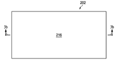
도 2는 예시적인 목표 패턴(200)을 도시한다. 목표 패턴(200)은 특징부(204a 내지 204c, 206a, 206b)를 포함한다. 예를 위해, 특징부(204a 내지 204c, 206a, 206b)는 X 방향으로 W의 그리고 Y 방향으로 L의 동일한 치수를 갖는 사실상 직사각형인 트렌치이다. 이들 특징부는 피치 P를 갖고 일렬로 배열된다. 목표 패턴(200)은 집적 회로(IC)의 다양한 구성요소를 형성하는데 이용될 수 있다. 일 실시예에서, 목표 패턴(200)은 다중 층 상호연결 구조체에 금속 라인을 형성하는데 이용된다. 다른 실시예에서, 목표 패턴(200)은 얕은 트렌치 격리(STI) 특징부를 위해 반도체 기판에 복수의 트렌치를 형성하는데 이용된다. 집적 회로의 밀도가 증가함에 따라, 몇몇 구성요소도 또한 마스크(또는 포토 마스크)의 해상도를 위해 함께 밀집될 수 있다. 이런 문제를 극복하기 위해, 스페이서 자체 정렬 패터닝 기술이 이용될 수도 있다. 본 발명의 실시예에서, 특징부(204a 내지 204c)는 마스크(또는 포토 마스크)를 이용하여 형성되지만, 특징부(206a, 206b)는 스페이서 특징부를 이용하여 형성될 것이다. FIG. 2 illustrates an
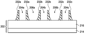
이하의 상세한 설명에서, 목표 패턴(200)이 본 발명의 다양한 양태에 따른 마스크와 스페이서 특징부를 이용하여 형성되는 방법을 도시하는 도 3a 내지 도 9b와 함께 본 발명의 방법(100)(도 1 참조)이 기술된다. 도 3a 내지 도 9b 각각에서, 접미사 "a"(예컨대, 도 3a 참조)가 표시된 구성요소는 접미사 "b," "c" 등(예컨대, 도 3b 참조)으로 표시된 구성요소에 대한 단면도를 한정하는 점선을 포함한다. In the following detailed description, the
본 발명의 방법(100)(도 1 참조)은 기판(202)을 제공함으로써 작업 102에서 개시된다. 도 3a 및 도 3b를 참조하면, 본 발명의 실시예에서 기판(202)은 재료 층(214, 216)을 포함한다. 재료 층(214, 216)은 비정질 실리콘(a-Si), 실리콘 산화물, 실리콘 질화물(SiN), 무질소 반사 방지 코팅(NFARC), 스핀 온 유리(SOG), 티타늄 질화물, 또는 다른 적절한 재료 또는 조성물을 사용할 수 있다. 재료 층(214, 216)은 다양한 공정에 의해 형성될 수 있다. 예컨대, 재료 층(214)은 퇴적(deposition)과 같은 방법에 의해 다른 기판 위에 형성될 수도 있다. 일 실시예에서, 재료 층(216)은 열산화에 의해 형성된 실리콘 산화물을 포함할 수 있다. 일 실시예에서, 재료 층(216)은 화학 증착(CVD)에 의해 형성된 SiN을 포함할 수 있다. 예컨대, 재료 층(216)은 헥사클로로디실란(HCD 또는 Si2Cl6), 디클로로실란(DCS 또는 SiH2Cl2), 비스(삼차부틸아미노) 실란(BTBAS 또는 C8H22N2Si), 및 디실란(DS 또는 Si2H6)을 포함하는 케미컬을 사용하는 CVD에 의해 형성될 수도 있다. 재료 층(214, 216)은 유사한 또는 상이한 방법에 의해 형성될 수도 있다. 상술된 재료 층(214, 216)의 예시적인 조성은 신규한 본 발명의 범주를 제한하는 것이 아니다. The
본 발명의 방법(100)(도 1 참조)은 포토리소그래피 공정을 포함하는 공정과 같은 적절한 공정을 통해 마스크를 이용하여 기판(202) 위에 맨드릴(mandrel) 라인을 형성함으로써 작업 104로 진행된다. 도 4a 및 도 4b를 참조하면, 맨드릴 라인(218a 내지 218c)은 기판(202) 위에 형성된다. 맨드릴 라인(218a 내지 218c) 각각은 특징부(204a 내지 204c)(도 2 참조)에 대응하는 마스크에 피치 Pm를 갖고 형성된다. The
일 실시예에서, 맨드릴 라인(218a 내지 218c)은 포토리소그래피 공정에서 네가티브 또는 파지티브 레지스트(또는 포토레지스트) 재료에 형성된다. 예시적인 포토리소그래피 공정은 네가티브 레지스트 층(218)을 재료 층(216) 위에 코팅하는 단계와, 레지스트 층(218)을 소프트 베이킹하는 단계와, 마스크를 이용하여 디프 자외선(DUV) 광에 레지스트 층(218)을 노출시키는 단계를 포함한다. 또한, 포토리소그래피 공정은 노출후 베이킹(PEB) 단계와, 현상 단계와, 하드 베이킹하여 레지스트 층(218)의 비노출 부분을 제거하고 레지스트 층(218)의 노출 부분을 맨드릴 라인으로서 기판(202) 상에 남겨두는 단계를 포함한다. 다른 실시예에서, 맨드릴 라인(218a 내지 218c)은 유사한 포토리소그래피 공정에서 파지티브 레지스트 재료 층의 비노출 부분에 의해 형성될 수도 있다. In one embodiment,
몇몇 경우에, 마스크 내의 특징부는 목표 패턴(200)(도 2 참조)의 대응하는 특징부보다 클 수도 있다. 이런 경우, 작업 104는 X 방향과 Y 방향 양자 모두에서 특징부(218a 내지 218c)의 치수를 트리밍하도록 트리밍 공정을 더 포함할수도 있다. In some cases, the features in the mask may be larger than the corresponding features of the target pattern 200 (see FIG. 2). In this case, the
특징부(218a 내지 218c)가 포토리소그래피 공정에서 형성되는 경우, 푸팅(footing) 문제가 야기될 수도 있다. 도 4b에 도시된 바와 같이, 맨드릴 라인(218a)의 바닥부에서, 레지스트 재료(218)는 재료 층(216)과 함께 직각이 아닌 둔각을 형성한다. 푸팅이 문제가 되는 하나의 이유는 레지스트 재료(218)가 재료 층(216)에 부착되어 제거가 힘들어지는 것일 수 있다. 다른 이유는 피치 Pm은 너무 작지만 맨드릴 라인(218a 내지 218c)은 상대적으로 커서, 레지스트 현상 해상도로는 맨드릴 라인(218a 내지 218c)의 바닥부에 도달하기 어렵다는 것이다. 이런 문제는 집적 회로 패턴 밀도가 14㎚, 10㎚, 및 그 이상과 같이 후기 공정 노드에서 계속 증가하는 경우에 더 심해질 수 있다. If the
본 발명의 방법(100)(도 1 참조)은 기판(202) 위에 그리고 맨드릴 라인(218a 내지 218c) 위로 걸쳐 스페이서 층(220)을 형성함으로써 작업 106으로 진행된다. 도 5a 및 도 5b를 참조하면, 스페이서 층(220)은 기판(202) 위에, 보다 구체적으로는 재료 층(216) 위에 형성된다. 또한, 스페이서 층(220)은 맨드릴 라인(218a 내지 218c) 위에 그리고 맨드릴 라인(218a 내지 218c)의 측벽 상에 형성된다. 스페이서 층(220)은 제1 두께 T1을 갖는다. 스페이서 층(220)은 재료 층(216)과 맨드릴 라인(218a 내지 218c)과 상이한 하나 이상의 재료 또는 조성물을 포함한다. 일 실시예에서, 스페이서 층(220)은 티타늄 질화물, 실리콘 질화물, 실리콘 산화물 또는 티타늄 산화물과 같은 유전체 재료를 포함할 수도 있다. 스페이서 층(220)은 퇴적 공정과 같은 적절한 공정에 의해 형성될 수 있다. 예컨대, 퇴적 공정은 화학 증착(CVD) 공정 또는 물리 증착(PVD) 공정을 포함한다. 도 5b에 도시된 바와 같이, 부분적으로는 상술된 푸팅 문제로 인해, 재료 층(216) 위에 배치된 스페이서 재료는 특징부(218a 내지 218c)의 측벽 상에 배치된 스페이스 재료와 함께 직각이 아닌 둔각을 형성한다. 몇몇 경우에, 스페이서 층(220)의 퇴적은 푸팅 문제를 악화시킬 수도 있다. The
본 발명의 방법(100)(도 1 참조)은 맨드릴 라인(218a 내지 218c)과 재료 층(216)을 노출시키기 위해 스페이서 층(220)을 에칭함으로써 작업 108로 진행된다. 도 6a 및 도 6b를 참조하면, 맨드릴 라인(218a 내지 218c)의 상부면이 이 에칭 공정에 의해 노출되고 그리고 재료 층(216) 위에 배치된 스페이서 재료가 또한 부분적으로 제거되어, 맨드릴 라인(218a 내지 218c)의 측벽 상에 스페이서 특징부(220a 내지 220c)를 각각 제공한다. X 방향으로 치수 S1을 갖는 2개의 트렌치(228a, 228b)가 스페이서 특징부들(220a 내지 220c) 사이에 형성된다. 일 실시예에서, 스페이서 층(220)의 에칭 공정은 건식(또는 플라즈마) 에칭과 같은 이방성 에칭을 포함한다. 예컨대, 건식 에칭 공정은 산소 함유 가스, 플루오르 함유 가스(예컨대, CF4, SF6, CH2F2, CHF3 및/또는 C2F6), 염소 함유 가스(예컨대, Cl2, CHCl3, CCl4 및/또는 BCl3), 브롬 함유 가스(예컨대, HBr 및/또는 CHBR3), 요오드 함유 가스, 다른 적절한 가스 및/또는 플라즈마, 및/또는 이들의 조합물을 실시할 수도 있다. The
또한 도 6a에 도시된 점선은 도 2의 목표 특징부(204a 내지 204c, 206a, 206b)이다. 특징부(218a 내지 218c)가 존재하는 위치에 형성되는 목표 특징부(204a 내지 204c)는 소정의 치수를 가질 것이다. 그러나, 트렌치(228a, 228b) 내에 형성되는 목표 특징부(206a, 206b)는 X 방향으로의 소정의 치수 W보다 사실상 작은 치수(S1)를 가질 것이다. 이런 이유는 상술된 푸팅 문제(도 4b 및 도 5b 참조)에 부분적으로 기인한다. 또한, 스페이서 층(220)에 적용된 건식 에칭 공정은 스페이서 특징부의 상부 및 바닥부에서 상이한 에칭률을 가질 수도 있다. 몇몇 경우에, 특히 조밀한 스페이서 특징부를 갖는 경우에, 건식 에칭 공정은 스페이서 특징부의 바닥부에서보다 상부에서 더 많은 스페이서 재료를 제거할 수도 있다. 이로 인해 푸팅 문제가 더 악화되어, 목표 치수 W보다 사실상 작은 치수 S1이 형성된다. Also, the dotted lines shown in Fig. 6A are the target features 204a to 204c, 206a, and 206b of Fig. The target features 204a-204c formed at the locations where the
본 발명의 방법(100)(도 1 참조)은 치수 W에 일치하도록 X 방향으로의 트렌치(228a, 228b)의 치수를 증가시키기 위해 스페이서 특징부(220a 내지 220c)를 수축(shrinking)시킴으로써 작업 110으로 진행된다. 본 실시예에서, 습식 세정 공정이 스페이서 특징부(220a 내지 220c)에 적용되어, 맨드릴 라인(218a 내지 218c)과 재료 층(216)의 실질적인 변경 없이 스페이서 특징부(220a 내지 220c)의 치수를 감소시킨다. The
도 7a 및 도 7b를 참조하면, 편의를 위해 감소된 스페이서 특징부는 도면부호 232a 내지 232c로 표시되어 있지만, 원래의 스페이서 특징부(220a 내지 220c)의 외부면의 일부(도 7b 참조)는 비교를 위해 점선으로 표시되어 있다. 습식 세정 공정의 결과로서, 트렌치(228a, 228b)는 사실상 일치하는 목표 특징부(206a, 206b)로 확대되어 있다. 본 실시예에서, 습식 세정 공정이 스페이서 재료를 부분적으로 제거하기 위해 선택적으로 조정되는 세정액을 도포하는 동안, 맨드릴 라인(218a 내지 218c)과 재료 층(216)은 사실상 변경되지 않은 상태로 유지된다. 스페이서 재료로서 티타늄 질화물 또는 티타늄 산화물을 사용하는 실시예에서, 습식 에칭 공정은 pH가 3 내지 6의 범위인 플루오르화 수소산(HF)과 같은 산용액, pH가 8 내지 10의 범위인 SCl 용액[예컨대, 수산화암모늄(NH4OH), 과산화수소(H2O2) 및 물(H2O)의 1:1:5 혼합물]과 같은 기본 용액을 적용한다. HF 또는 SCl 용액은 60℃ 이하의 온도, 예컨대 약 25℃ 내지 60℃의 온도에서 소정의 스페이서 재료에 대한 약 10 내지 30의 분당 옹스트롬의 에칭률을 제공한다. 더 높은 에칭귤은 더 높은 온도, 예컨대 약 60℃ 내지 80℃의 온도에서 달성된다. 스페이서 재료로서 실리콘 질화물을 사용하는 다른 실시예에선, 습식 세정 공정은 pH가 3 내지 6의 범위인 HF 또는 인산(H2PO4 -)과 같은 산용액이 적용되는데, 이런 산용액은 60℃ 이하의 온도, 예컨대 약 25℃ 내지 60℃의 온도에서 약 10 내지 20의 분당 옹스트롬에서 소정의 스페이서 재료에 대한 에칭률을 제공한다. 더 높은 에칭귤은 더 높은 온도, 예컨대 약 60℃ 내지 80℃의 온도에서 달성된다. 스페이서 특징부(220a 내지 220c)의 축소 이외에도, 습식 세정 공정은 스페이서 에칭 공정으로 인한 임의의 잔류물을 재료 층(216)으로부터 제거하는 추가의 이점을 제공한다. 7A and 7B, a portion of the outer surface of the original spacer features 220a-220c (see FIG. 7B) is shown as being comparable, although for simplicity the reduced spacer features are represented by
본 발명의 방법(100)(도 1 참조)은 맨드릴 라인(218a 내지 218c)을 제거함으로써 작업 112로 진행된다. 도 8a 내지 도 8b를 참조하면, 맨드릴 라인(218a 내지 218c)이 제거되어 있다. 스페이서 특징부(232a 내지 232c)는 기판(202) 위에 5개의 트렌치(204a 내지 204c, 206a, 206b)를 형성한다. 맨드릴 라인(218a 내지 218c)은 맨드릴 라인(218a 내지 218c)을 선택적으로 제거하도록 조정되는 공정을 이용하여 제거되지만, 스페이서 특징부(232a 내지 232c)는 남겨진다. 일 실시예에서, 맨드릴 라인(218a 내지 218c)은 레지스트 재료를 사용하며, 맨드릴 라인(218a 내지 218c)을 제거하는 공정은 습식 스트리핑 또는 플라즈마 애싱(plasma ashing)을 이용한다. The
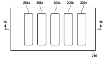
본 발명의 방법(100)(도 1 참조)은 이방성 에칭과 같은 적절한 공정을 이용하여 패턴을 스페이서 특징부(232a 내지 232c)로부터 재료 층(216)으로 전사함으로써 작업 114로 진행된다. 후속하여, 스페이서 특징부(232a 내지 232c)가 제거되어, 목표 패턴(200)(도 2 참조)에 일치하는 패턴이 재료 층(216)에 형성된다(도 9a 및 도 9b 참조). The
본 발명의 방법(100)(도 1 참조)은 패터닝된 재료 층(216)을 이용하여 최종 패턴 또는 디바이스를 형성하기 위해 작업 116으로 진행된다. 일 실시예에서, 목표 패턴은 다중 층 상호연결 구조의 금속 라인으로서 형성될 것이다. 예컨대, 금속 라인은 내부층 유전체(ILD) 층에 형성될 수도 있다. 이런 경우, 작업 116에서, 패터닝된 재료 층(216)을 이용하여 ILD 층에 복수의 트렌치를 형성하고, 금속과 같은 전도성 재료로 트렌치를 충전하고, 패터닝된 ILD 층을 노출시키기 위해 화학 기계적 연마와 같은 공정을 이용하여 전도성 물질을 연마함으로써, ILD 라인에 금속 라인을 형성한다. The
다른 실시예에서, 작업 116에서, 패터닝된 재료 층(216)을 이용하여 반도체 기판 상에 핀 구조 전계 효과 트랜지스터(FinFET) 구조를 형성한다. 이 실시예에서는, 작업 116에서 반도체 기판에 복수의 트렌치를 형성한다. 또한, 유전체 재료로 트렌치를 충전하기 위한 퇴적 단계와, 초과 유전체 재료를 제거하고 반도체 기판의 상부면을 평탄화하기 위한 (CMP와 같은)연마 단계를 포함하는 방법에 의해 얕은 트렌치 격리(STI) 특징부가 트렌치에 형성된다. 후속하여, STI 특징부를 리세싱하여(recess) 핀형(fin-like) 활성 구역을 형성하기 위해 선택적 에칭 공정이 유전체 재료에 적용된다. In another embodiment, at
당업자들이 본 발명의 양태를 더 잘 이해할 수 있도록 몇몇 실시예에 대한 상술된 구성요소가 개시되어 있다. 당업자들은 본 명세서에 개시된 실시예의 동일한 목적 및/또는 이점을 달성하기 위해 다른 공정 및 구조를 설계하거나 변경하기 위한 기초로서 본 명세서의 내용을 용이하게 이용할 수 있을 것이다. 또한, 당업자들은 그런 등가 구성들은 본 발명의 기술 사상 및 범주를 벗어나지 않음을 알 것이며, 본 발명의 기술 사상 및 범주 내에서 다양한 변형예, 대체예 및 변경예를 실시할 수 있을 것이다. In order that those skilled in the art will be better able to understand aspects of the present invention, the above described components for some embodiments are disclosed. Skilled artisans may readily utilize the teachings herein as a basis for designing or modifying other processes and structures to accomplish the same objects and / or advantages of the embodiments disclosed herein. Those skilled in the art will also appreciate that such equivalent constructions do not depart from the spirit and scope of the present invention and that various modifications, substitutions and alterations can be made within the spirit and scope of the present invention.
본 발명의 예시적인 일 양태는 집적 회로(IC)를 위한 목표 패턴을 형성하는 방법에 관한 것이다. 본 발명의 방법은 제1 마스크를 이용하여 복수의 라인을 기판 위에 형성하는 단계와, 기판 위에, 복수의 라인 위에 그리고 복수의 라인의 측벽 상에 스페이서 층을 형성하는 단계를 포함한다. 또한, 본 발명의 방법은 복수의 라인과 기판을 노출시키기 위해 스페이서 층의 적어도 일부를 제거하는 단계를 포함한다. 또한, 본 발명의 방법은 복수의 라인의 측벽 상에 배치되는 스페이서 층을 수축시키는 단계와, 복수의 라인을 제거함으로써 패터닝된 스페이서 층을 기판 위에 제공하는 단계를 포함한다. One illustrative aspect of the present invention is directed to a method of forming a target pattern for an integrated circuit (IC). The method includes forming a plurality of lines on a substrate using a first mask and forming a spacer layer over the plurality of lines and on the sidewalls of the plurality of lines on the substrate. The method of the present invention also includes removing at least a portion of the spacer layer to expose the plurality of lines and the substrate. The method also includes contraction of the spacer layer disposed on the sidewalls of the plurality of lines and providing the patterned spacer layer on the substrate by removing the plurality of lines.
본 발명의 예시적인 다른 양태는 집적 회로(IC)를 위한 목표 패턴을 형성하는 방법에 관한 것이다. 본 발명의 방법은 제1 마스크를 이용하여 기판을 패터닝함으로써 제1의 복수의 특징부를 형성하는 단계와, 기판 위에 그리고 제1의 복수의 특징부의 측벽 위에 스페이서 층을 형성하는 단계를 포함한다. 또한, 본 발명의 방법은 제1의 복수의 특징부를 노출시키고 상기 기판을 노출시키기 위해 스페이서 층의 적어도 일부를 이방성 에칭하는 단계를 포함한다. 또한, 본 발명의 방법은 스페이서 층의 두께를 제어가능한 방식으로 감소시키기 위해 화학 용액을 이용하여 스페이서 층을 세정하는 단계와, 제1의 복수의 특징부를 제거하는 단계를 포함한다. Another exemplary aspect of the invention relates to a method of forming a target pattern for an integrated circuit (IC). The method of the present invention includes forming a first plurality of features by patterning the substrate using a first mask and forming a spacer layer on the substrate and over the sidewalls of the first plurality of features. The method of the present invention also includes anisotropically etching at least a portion of the spacer layer to expose the first plurality of features and expose the substrate. The method also includes cleaning the spacer layer with a chemical solution to reduce the thickness of the spacer layer in a controllable manner, and removing the first plurality of features.
본 발명의 예시적인 또 다른 양태는 기판 상에 패턴을 형성하는 방법에 관한 것이다. 본 발명의 방법은 제1 방향으로 제1 치수를 갖는 2개의 라인을 포토리소그래피 공정을 이용하여 기판 위에 형성하는 단계를 포함한다. 또한, 본 발명의 방법은 기판 위에, 2개의 라인 위에 그리고 2개의 라인의 측벽 상에 제1 재료를 퇴적시키는 단계를 포함한다. 또한, 본 발명의 방법은 기판과 2개의 라인을 노출시키기 위해 제1 재료에 이방성 에칭 공정을 수행하는 단계를 포함한다. 또한, 본 발명의 방법은 제1 재료의 두께를 감소시켜 2개의 라인의 측벽 상에 배치되는 제1 재료가 제1 방향으로 제2 치수만큼 이격되도록 제1 재료에 습식 세정 공정을 수행하는 단계와, 2개의 라인을 제거하는 단계를 포함한다. Another exemplary aspect of the present invention relates to a method of forming a pattern on a substrate. The method includes forming two lines having a first dimension in a first direction on a substrate using a photolithographic process. The method of the present invention also includes depositing a first material on the substrate, over the two lines and on the sidewalls of the two lines. The method also includes performing an anisotropic etch process on the first material to expose the substrate and the two lines. The method also includes performing a wet cleaning process on the first material to reduce the thickness of the first material so that the first material disposed on the sidewalls of the two lines is spaced apart by a second dimension in the first direction , And removing the two lines.
200 : 목표 패턴
202 : 기판
218a, 218b, 218c : 맨드릴 라인
216 : 재료 층
220 : 스페이서 층 200: target pattern
202: substrate
218a, 218b, 218c: mandrel line
216: material layer
220: spacer layer
Claims (9)
제1 마스크를 이용하여 복수의 라인들을 기판 위에 형성하는 단계;
상기 기판 위에, 복수의 라인들 위에 그리고 복수의 라인들의 측벽들 상에 스페이서 층을 형성하는 단계;
상기 복수의 라인들의 상면과 상기 기판의 일부를 노출시키기 위해 건식 에칭 공정을 이용하여 상기 스페이서 층의 적어도 일부를 제거하는 단계로서, 상기 복수의 라인들의 측벽들 상에 스페이서 특징부들을 형성하고, 상기 스페이서 특징부들 사이에 그리고 상기 기판 상에 트렌치들이 형성되는, 상기 스페이서 층의 적어도 일부를 제거하는 단계;
상기 스페이서 층의 적어도 일부를 제거하는 단계 이후에, 상기 트렌치들의 폭이 상기 복수의 라인들의 폭과 동일해지도록 상기 복수의 라인들의 측벽들 상의 상기 스페이서 특징부들을 수축시키는 단계로서, 상기 스페이서 특징부들의 수축은 등방성이며, 상기 복수의 라인들과 상기 기판은 변경되지 않으면서 상기 스페이서 특징부들의 일부를 제거하기 위해 선택적으로 조정되는(tuned) 세정 용액을 이용하는 습식 세정 공정을 포함하는 것인, 상기 스페이서 특징부들을 수축시키는 단계; 및
상기 스페이서 특징부들을 수축시킨 후에, 상기 복수의 라인들을 제거함으로써 패터닝된 스페이서 층을 기판 위에 제공하는 단계
를 포함하는 집적 회로를 위한 목표 패턴 형성 방법.A method of forming a target pattern for an integrated circuit,
Forming a plurality of lines on the substrate using a first mask;
Forming a spacer layer on the substrate over a plurality of lines and on sidewalls of the plurality of lines;
Removing at least a portion of the spacer layer using a dry etch process to expose an upper surface of the plurality of lines and a portion of the substrate to form spacer features on the sidewalls of the plurality of lines, Removing at least a portion of the spacer layer, wherein trenches are formed between the spacer features and on the substrate;
Shrinking the spacer features on the sidewalls of the plurality of lines such that the width of the trenches is equal to the width of the plurality of lines after removing at least a portion of the spacer layer, Wherein the shrinkage of the spacer features is isotropic and wherein the plurality of lines and the substrate are not altered and are selectively tuned to remove a portion of the spacer features. Contracting the spacer features; And
Providing a patterned spacer layer on the substrate by removing the plurality of lines after shrinking the spacer features,
Gt; a < / RTI > target pattern for an integrated circuit.
적어도 상기 패터닝된 스페이서 층을 에칭 마스크로서 이용하여 상기 기판을 에칭하는 단계; 및
상기 에칭 후에 상기 패터닝된 스페이서 층을 제거하는 단계를 더 포함하는 집적 회로를 위한 목표 패턴 형성 방법.The method according to claim 1,
Etching said substrate using at least said patterned spacer layer as an etch mask; And
And removing the patterned spacer layer after the etching. ≪ Desc / Clms Page number 22 >
상기 복수의 라인들을 형성하는 단계는,
상기 기판 위에 레지스트 층을 형성하는 단계; 및
상기 제1 마스크를 이용하여 상기 레지스트 층을 패터닝하는 단계를 포함하는 것인, 집적 회로를 위한 목표 패턴 형성 방법.The method according to claim 1,
Wherein forming the plurality of lines comprises:
Forming a resist layer on the substrate; And
And patterning the resist layer using the first mask. ≪ Desc / Clms Page number 20 >
상기 건식 에칭 공정은 이방성 에칭 공정을 포함하는 것인, 집적 회로를 위한 목표 패턴 형성 방법.The method according to claim 1,
Wherein the dry etching process comprises an anisotropic etch process.
상기 스페이서 층은 티타늄 질화물 또는 티타늄 산화물을 포함하고,
상기 습식 세정 공정은 플루오르화 수소산(HF) 또는 SCl 용액을 이용하는 것인, 집적 회로를 위한 목표 패턴 형성 방법.The method according to claim 1,
Wherein the spacer layer comprises titanium nitride or titanium oxide,
Wherein the wet scrubbing process utilizes a hydrofluoric acid (HF) or SCl solution.
상기 스페이서 층은 실리콘 질화물을 포함하고,
상기 습식 세정 공정은 플루오르화 수소산(HF) 또는 인산(H2PO4 -)을 이용하는 것인, 집적 회로를 위한 목표 패턴 형성 방법.The method according to claim 1,
Wherein the spacer layer comprises silicon nitride,
Wherein the wet scrubbing process utilizes hydrofluoric acid (HF) or phosphoric acid (H 2 PO 4 - ).
상기 스페이서 층을 형성하기 전에 상기 복수의 라인들을 트리밍하는 단계를 더 포함하는, 집적 회로를 위한 목표 패턴 형성 방법.The method according to claim 1,
Further comprising the step of trimming the plurality of lines prior to forming the spacer layer.
제1 마스크를 이용하여 기판을 패터닝함으로써 제1의 복수의 특징부들을 형성하는 단계;
상기 기판 위에, 상기 제1의 복수의 특징부들들 위에, 그리고 상기 제1의 복수의 특징부들의 측벽들 상에 스페이서 층을 형성하는 단계;
상기 제1의 복수의 특징부들의 상면과 상기 기판의 일부를 노출시키기 위해 상기 스페이서 층의 적어도 일부에 대해 건식 에칭 공정을 수행하는 단계로서, 상기 제1의 복수의 특징부들의 측벽들 상에 스페이서 특징부들을 형성하고, 상기 스페이서 특징부들 사이에 그리고 상기 기판 상에 트렌치들이 형성되는, 상기 건식 에칭 공정을 수행하는 단계;
상기 스페이서 층의 적어도 일부에 대해 건식 에칭 공정을 수행하는 단계 이후에, 상기 트렌치들의 폭이 상기 제1의 복수의 특징부들의 폭과 동일해지도록, 상기 제1의 복수의 특징부들과 상기 기판이 변경되지 않게 유지하면서 상기 스페이서 특징부들의 두께를 등방성으로 감소시키기 위해 상기 스페이서 특징부들에 대해 선택적으로 조정되는(tuned) 세정 용액을 이용하는 습식 세정 공정을 수행하는 단계; 및
상기 습식 세정 공정을 수행한 후에, 상기 제1 복수의 특징부들을 제거하는 단계
를 포함하는 집적 회로를 위한 목표 패턴 형성 방법.A method of forming a target pattern for an integrated circuit,
Forming a first plurality of features by patterning the substrate using a first mask;
Forming a spacer layer on the substrate over the first plurality of features and on the sidewalls of the first plurality of features;
Performing a dry etch process on at least a portion of the spacer layer to expose an upper surface of the first plurality of features and a portion of the substrate, Performing the dry etching process wherein features are formed and trenches are formed between the spacer features and on the substrate;
Wherein after the step of performing a dry etching process on at least a portion of the spacer layer, the width of the trenches is equal to the width of the first plurality of features, Performing a wet cleaning process using a cleaning solution that is selectively tuned to the spacer features to reduce the thickness of the spacer features isotropically while remaining unaltered; And
Removing the first plurality of features after performing the wet scrubbing process
Gt; a < / RTI > target pattern for an integrated circuit.
제1 방향으로 제1 치수를 갖는 2개의 라인을 포토리소그래피 공정을 이용하여 기판 위에 형성하는 단계;
상기 기판 위에, 상기 2개의 라인 위에 그리고 상기 2개의 라인의 측벽들 상에 제1 재료를 성막하는 단계;
상기 2개의 라인의 상면과 상기 기판의 일부를 노출시키기 위해 상기 제1 재료에 대해 건식 에칭 공정을 수행하는 단계;
상기 제1 재료에 대해 건신 에칭 공정을 수행하는 단계 이후에, 상기 2개의 라인과 상기 기판은 변경되지 않으면서, 상기 2개의 라인의 측벽들 상에 배치된 상기 제1 재료가 상기 제1 방향으로 제2 치수만큼 이격되도록 상기 제1 재료의 두께를 등방성으로 감소시키기 위해 상기 제1 재료에 대해 선택적으로 조정되는(tuned) 세정 용액을 이용하는 습식 세정 공정을 수행하는 단계로서, 상기 2개의 라인들 사이에서 상기 제2 치수를 갖는 상기 제1 재료 간의 거리가 상기 2개의 라인들의 상기 제1 치수와 동일한 것인, 상기 습식 세정 공정을 수행하는 단계; 및
상기 습식 세정 공정을 수행한 후에, 상기 2개의 라인을 제거하는 단계를 포함하는 집적 회로를 위한 목표 패턴 형성 방법.A method of forming a target pattern for an integrated circuit,
Forming two lines having a first dimension in a first direction on the substrate using a photolithography process;
Depositing a first material on the substrate, over the two lines and on the sidewalls of the two lines;
Performing a dry etching process on the first material to expose a top surface of the two lines and a portion of the substrate;
Wherein after the step of performing a dry etch process for the first material, the two lines and the substrate are unaltered, wherein the first material disposed on the sidewalls of the two lines is in the first direction Performing a wet cleaning process using a cleaning solution that is selectively tuned to the first material to reduce the thickness of the first material to be isotropically to be spaced apart by a second dimension, Wherein the distance between the first material having the second dimension is equal to the first dimension of the two lines; And
And removing the two lines after performing the wet cleaning process. ≪ Desc / Clms Page number 13 >
Applications Claiming Priority (2)
| Application Number | Priority Date | Filing Date | Title |
|---|---|---|---|
| US14/088,569 US9129814B2 (en) | 2013-11-25 | 2013-11-25 | Method for integrated circuit patterning |
| US14/088,569 | 2013-11-25 |
Related Parent Applications (1)
| Application Number | Title | Priority Date | Filing Date |
|---|---|---|---|
| KR1020170052439A Division KR20170047205A (en) | 2013-11-25 | 2017-04-24 | Method for integrated circuit patterning |
Publications (2)
| Publication Number | Publication Date |
|---|---|
| KR20180098481A true KR20180098481A (en) | 2018-09-04 |
| KR102010188B1 KR102010188B1 (en) | 2019-08-12 |
Family
ID=53183021
Family Applications (3)
| Application Number | Title | Priority Date | Filing Date |
|---|---|---|---|
| KR1020140165116A Ceased KR20150060577A (en) | 2013-11-25 | 2014-11-25 | Method for integrated circuit patterning |
| KR1020170052439A Ceased KR20170047205A (en) | 2013-11-25 | 2017-04-24 | Method for integrated circuit patterning |
| KR1020180095457A Active KR102010188B1 (en) | 2013-11-25 | 2018-08-16 | Method for integrated circuit patterning |
Family Applications Before (2)
| Application Number | Title | Priority Date | Filing Date |
|---|---|---|---|
| KR1020140165116A Ceased KR20150060577A (en) | 2013-11-25 | 2014-11-25 | Method for integrated circuit patterning |
| KR1020170052439A Ceased KR20170047205A (en) | 2013-11-25 | 2017-04-24 | Method for integrated circuit patterning |
Country Status (3)
| Country | Link |
|---|---|
| US (2) | US9129814B2 (en) |
| KR (3) | KR20150060577A (en) |
| CN (1) | CN104658892B (en) |
Families Citing this family (13)
| Publication number | Priority date | Publication date | Assignee | Title |
|---|---|---|---|---|
| RU2013117118A (en) * | 2010-09-16 | 2014-10-27 | Спекмет, Инк. | METHOD, PROCESS, AND TECHNOLOGY OF PRODUCTION OF HIGH-PERFORMANCE INEXPENSIVE CRYSTAL SILICON SOLAR ELEMENTS |
| US9373519B2 (en) * | 2013-12-04 | 2016-06-21 | Imec Vzw | Method to pattern substrates |
| US9524908B2 (en) * | 2014-04-01 | 2016-12-20 | Globalfoundries Inc. | Methods of removing portions of fins by preforming a selectively etchable material in the substrate |
| US9236481B1 (en) * | 2015-04-29 | 2016-01-12 | Globalfoundries Inc. | Semiconductor device and methods of forming fins and gates with ultraviolet curing |
| US10157742B2 (en) | 2015-12-31 | 2018-12-18 | Taiwan Semiconductor Manufacturing Co., Ltd. | Method for mandrel and spacer patterning |
| US10056256B2 (en) * | 2016-03-16 | 2018-08-21 | Taiwan Semiconductor Manufacturing Co., Ltd. | Method of priming photoresist before application of a shrink material in a lithography process |
| US10074657B2 (en) | 2016-04-28 | 2018-09-11 | Taiwan Semiconductor Manufacturing Company, Ltd. | Method of manufacturing fins and semiconductor device which includes fins |
| US10199265B2 (en) * | 2017-02-10 | 2019-02-05 | Globalfoundries Inc. | Variable space mandrel cut for self aligned double patterning |
| US11393674B2 (en) | 2018-05-18 | 2022-07-19 | Taiwan Semiconductor Manufacturing Company, Ltd. | Forming low-stress silicon nitride layer through hydrogen treatment |
| US10658179B2 (en) * | 2018-08-17 | 2020-05-19 | Taiwan Semiconductor Manufacturing Co., Ltd. | Method and structure of middle layer removal |
| US10483119B1 (en) * | 2018-09-20 | 2019-11-19 | Taiwan Semiconductor Manufacturing Co., Ltd. | Self-aligned double patterning (SADP) method |
| US10957604B2 (en) | 2018-10-31 | 2021-03-23 | Taiwan Semiconductor Manufacturing Company, Ltd. | Semiconductor device and method |
| CN110104609A (en) * | 2019-05-10 | 2019-08-09 | 中国科学院微电子研究所 | A kind of microelectrode and forming method thereof |
Citations (5)
| Publication number | Priority date | Publication date | Assignee | Title |
|---|---|---|---|---|
| KR20100058760A (en) * | 2008-11-25 | 2010-06-04 | 한국전자통신연구원 | Method of forming a semiconductor device unconstrained by optical limit and apparatus for fabricating thereof |
| KR20110099274A (en) * | 2008-11-24 | 2011-09-07 | 마이크론 테크놀로지, 인크. | Method of forming masking pattern for integrated circuit |
| KR20110111473A (en) * | 2009-01-07 | 2011-10-11 | 브레우어 사이언스 인코포레이션 | Pin-on spacer materials for double- and triple-patterned lithography |
| KR20130063348A (en) * | 2011-12-06 | 2013-06-14 | 삼성전자주식회사 | Method for forming pattern of semiconductor device |
| KR20130079295A (en) * | 2011-12-31 | 2013-07-10 | 롬 앤드 하스 일렉트로닉 머트어리얼즈, 엘.엘.씨. | Photoresist pattern trimming methods |
Family Cites Families (11)
| Publication number | Priority date | Publication date | Assignee | Title |
|---|---|---|---|---|
| US5328810A (en) * | 1990-05-07 | 1994-07-12 | Micron Technology, Inc. | Method for reducing, by a factor or 2-N, the minimum masking pitch of a photolithographic process |
| US5489548A (en) * | 1994-08-01 | 1996-02-06 | Texas Instruments Incorporated | Method of forming high-dielectric-constant material electrodes comprising sidewall spacers |
| US5869866A (en) * | 1996-12-06 | 1999-02-09 | Advanced Micro Devices, Inc. | Integrated circuit having sacrificial spacers for producing graded NMOS source/drain junctions possibly dissimilar from PMOS source/drain junctions |
| US6472283B1 (en) * | 1999-09-24 | 2002-10-29 | Advanced Micro Devices, Inc. | MOS transistor processing utilizing UV-nitride removable spacer and HF etch |
| US7250114B2 (en) * | 2003-05-30 | 2007-07-31 | Lam Research Corporation | Methods of finishing quartz glass surfaces and components made by the methods |
| AU2004284922B2 (en) * | 2003-10-21 | 2010-02-25 | Hollister Incorporated | Flushable body waste collection pouch, pouch-in-pouch appliance using the same, and method relating thereto |
| US7776744B2 (en) * | 2005-09-01 | 2010-08-17 | Micron Technology, Inc. | Pitch multiplication spacers and methods of forming the same |
| US7670914B2 (en) * | 2006-09-28 | 2010-03-02 | Globalfoundries Inc. | Methods for fabricating multiple finger transistors |
| US8043921B2 (en) * | 2009-03-25 | 2011-10-25 | Texas Instruments Incorporated | Nitride removal while protecting semiconductor surfaces for forming shallow junctions |
| US8099686B2 (en) * | 2009-03-27 | 2012-01-17 | Globalfoundries Inc. | CAD flow for 15nm/22nm multiple fine grained wimpy gate lengths in SIT gate flow |
| US9006107B2 (en) * | 2012-03-11 | 2015-04-14 | United Microelectronics Corp. | Patterned structure of semiconductor device and fabricating method thereof |
-
2013
- 2013-11-25 US US14/088,569 patent/US9129814B2/en active Active
-
2014
- 2014-11-25 KR KR1020140165116A patent/KR20150060577A/en not_active Ceased
- 2014-11-25 CN CN201410690095.4A patent/CN104658892B/en not_active Expired - Fee Related
-
2015
- 2015-09-04 US US14/846,112 patent/US9589800B2/en not_active Expired - Fee Related
-
2017
- 2017-04-24 KR KR1020170052439A patent/KR20170047205A/en not_active Ceased
-
2018
- 2018-08-16 KR KR1020180095457A patent/KR102010188B1/en active Active
Patent Citations (5)
| Publication number | Priority date | Publication date | Assignee | Title |
|---|---|---|---|---|
| KR20110099274A (en) * | 2008-11-24 | 2011-09-07 | 마이크론 테크놀로지, 인크. | Method of forming masking pattern for integrated circuit |
| KR20100058760A (en) * | 2008-11-25 | 2010-06-04 | 한국전자통신연구원 | Method of forming a semiconductor device unconstrained by optical limit and apparatus for fabricating thereof |
| KR20110111473A (en) * | 2009-01-07 | 2011-10-11 | 브레우어 사이언스 인코포레이션 | Pin-on spacer materials for double- and triple-patterned lithography |
| KR20130063348A (en) * | 2011-12-06 | 2013-06-14 | 삼성전자주식회사 | Method for forming pattern of semiconductor device |
| KR20130079295A (en) * | 2011-12-31 | 2013-07-10 | 롬 앤드 하스 일렉트로닉 머트어리얼즈, 엘.엘.씨. | Photoresist pattern trimming methods |
Also Published As
| Publication number | Publication date |
|---|---|
| US20150147886A1 (en) | 2015-05-28 |
| CN104658892A (en) | 2015-05-27 |
| KR20170047205A (en) | 2017-05-04 |
| US9589800B2 (en) | 2017-03-07 |
| US20160071730A1 (en) | 2016-03-10 |
| US9129814B2 (en) | 2015-09-08 |
| KR102010188B1 (en) | 2019-08-12 |
| KR20150060577A (en) | 2015-06-03 |
| CN104658892B (en) | 2018-02-27 |
Similar Documents
| Publication | Publication Date | Title |
|---|---|---|
| KR102010188B1 (en) | Method for integrated circuit patterning | |
| KR101670556B1 (en) | Method for integrated circuit patterning | |
| KR101576335B1 (en) | Method for integrated circuit patterning | |
| US9418862B2 (en) | Method for integrated circuit patterning | |
| US7989355B2 (en) | Method of pitch halving | |
| US9153478B2 (en) | Spacer etching process for integrated circuit design | |
| US10727061B2 (en) | Method for integrated circuit patterning | |
| CN101681811B (en) | Method of isolating array features during pitch doubling process and semiconductor device structure having isolated array features | |
| CN105895510A (en) | Method for forming semiconductor device and patterning method | |
| TWI567785B (en) | Method for fabricating patterned structure of semiconductor device | |
| CN114334619A (en) | Method of forming a semiconductor structure | |
| CN103390551B (en) | Method for fabricating patterned structure of semiconductor device | |
| US8524608B1 (en) | Method for fabricating a patterned structure of a semiconductor device | |
| TW202147398A (en) | Method for forming semiconductor device | |
| CN110648959A (en) | Semiconductor device and method of manufacturing the same | |
| TWI518743B (en) | Method for fabricating patterned structure of semiconductor device |
Legal Events
| Date | Code | Title | Description |
|---|---|---|---|
| A107 | Divisional application of patent | ||
| A201 | Request for examination | ||
| PA0107 | Divisional application |
St.27 status event code: A-0-1-A10-A18-div-PA0107 St.27 status event code: A-0-1-A10-A16-div-PA0107 |
|
| PA0201 | Request for examination |
St.27 status event code: A-1-2-D10-D11-exm-PA0201 |
|
| PG1501 | Laying open of application |
St.27 status event code: A-1-1-Q10-Q12-nap-PG1501 |
|
| E902 | Notification of reason for refusal | ||
| PE0902 | Notice of grounds for rejection |
St.27 status event code: A-1-2-D10-D21-exm-PE0902 |
|
| T11-X000 | Administrative time limit extension requested |
St.27 status event code: U-3-3-T10-T11-oth-X000 |
|
| P11-X000 | Amendment of application requested |
St.27 status event code: A-2-2-P10-P11-nap-X000 |
|
| P13-X000 | Application amended |
St.27 status event code: A-2-2-P10-P13-nap-X000 |
|
| E701 | Decision to grant or registration of patent right | ||
| PE0701 | Decision of registration |
St.27 status event code: A-1-2-D10-D22-exm-PE0701 |
|
| GRNT | Written decision to grant | ||
| PR0701 | Registration of establishment |
St.27 status event code: A-2-4-F10-F11-exm-PR0701 |
|
| PR1002 | Payment of registration fee |
St.27 status event code: A-2-2-U10-U11-oth-PR1002 Fee payment year number: 1 |
|
| PG1601 | Publication of registration |
St.27 status event code: A-4-4-Q10-Q13-nap-PG1601 |
|
| R18-X000 | Changes to party contact information recorded |
St.27 status event code: A-5-5-R10-R18-oth-X000 |
|
| PR1001 | Payment of annual fee |
St.27 status event code: A-4-4-U10-U11-oth-PR1001 Fee payment year number: 4 |
|
| PR1001 | Payment of annual fee |
St.27 status event code: A-4-4-U10-U11-oth-PR1001 Fee payment year number: 5 |
|
| PR1001 | Payment of annual fee |
St.27 status event code: A-4-4-U10-U11-oth-PR1001 Fee payment year number: 6 |
|
| PR1001 | Payment of annual fee |
St.27 status event code: A-4-4-U10-U11-oth-PR1001 Fee payment year number: 7 |
|
| U11 | Full renewal or maintenance fee paid |
Free format text: ST27 STATUS EVENT CODE: A-4-4-U10-U11-OTH-PR1001 (AS PROVIDED BY THE NATIONAL OFFICE) Year of fee payment: 7 |
|
| P22-X000 | Classification modified |
St.27 status event code: A-4-4-P10-P22-nap-X000 |