US9524908B2 - Methods of removing portions of fins by preforming a selectively etchable material in the substrate - Google Patents
Methods of removing portions of fins by preforming a selectively etchable material in the substrate Download PDFInfo
- Publication number
- US9524908B2 US9524908B2 US14/242,529 US201414242529A US9524908B2 US 9524908 B2 US9524908 B2 US 9524908B2 US 201414242529 A US201414242529 A US 201414242529A US 9524908 B2 US9524908 B2 US 9524908B2
- Authority
- US
- United States
- Prior art keywords
- sacrificial material
- substrate
- fin
- etching process
- masking layer
- Prior art date
- Legal status (The legal status is an assumption and is not a legal conclusion. Google has not performed a legal analysis and makes no representation as to the accuracy of the status listed.)
- Active, expires
Links
Images


Classifications
-
- H01L21/823431—
-
- H—ELECTRICITY
- H10—SEMICONDUCTOR DEVICES; ELECTRIC SOLID-STATE DEVICES NOT OTHERWISE PROVIDED FOR
- H10D—INORGANIC ELECTRIC SEMICONDUCTOR DEVICES
- H10D84/00—Integrated devices formed in or on semiconductor substrates that comprise only semiconducting layers, e.g. on Si wafers or on GaAs-on-Si wafers
- H10D84/01—Manufacture or treatment
- H10D84/0123—Integrating together multiple components covered by H10D12/00 or H10D30/00, e.g. integrating multiple IGBTs
- H10D84/0126—Integrating together multiple components covered by H10D12/00 or H10D30/00, e.g. integrating multiple IGBTs the components including insulated gates, e.g. IGFETs
- H10D84/0158—Integrating together multiple components covered by H10D12/00 or H10D30/00, e.g. integrating multiple IGBTs the components including insulated gates, e.g. IGFETs the components including FinFETs
-
- H—ELECTRICITY
- H10—SEMICONDUCTOR DEVICES; ELECTRIC SOLID-STATE DEVICES NOT OTHERWISE PROVIDED FOR
- H10D—INORGANIC ELECTRIC SEMICONDUCTOR DEVICES
- H10D84/00—Integrated devices formed in or on semiconductor substrates that comprise only semiconducting layers, e.g. on Si wafers or on GaAs-on-Si wafers
- H10D84/01—Manufacture or treatment
- H10D84/02—Manufacture or treatment characterised by using material-based technologies
- H10D84/03—Manufacture or treatment characterised by using material-based technologies using Group IV technology, e.g. silicon technology or silicon-carbide [SiC] technology
- H10D84/038—Manufacture or treatment characterised by using material-based technologies using Group IV technology, e.g. silicon technology or silicon-carbide [SiC] technology using silicon technology, e.g. SiGe
Definitions
- the present disclosure relates to the manufacture of semiconductor devices, and, more specifically, to various methods of forming fins for FinFET semiconductor devices wherein the removal of portions of the fins is accomplished by preforming a selectively etchable material in the substrate at the location of the to-be-removed portions of the fins.
- CMOS technology is presently a preferred manufacturing technique in view of device performance and/or power consumption and/or cost efficiency.
- FETs field effect transistors
- the transistor devices exhibit a highly conductive state (on-state) and a high impedance state (off-state).
- the state of the field effect transistor is controlled by a gate electrode, which controls, upon application of an appropriate control voltage, the conductivity of a channel region formed between a drain region and a source region.
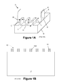
- FIG. 1A is a perspective view of an illustrative prior art FinFET semiconductor device “A” that is formed above a semiconductor substrate B that will be referenced so as to explain, at a very high level, some basic features of a FinFET device.
- the FinFET device A includes three illustrative fins C, a gate structure D, sidewall spacers E and a gate cap layer F. Trenches T are formed in the substrate B to define the fins C.
- the gate structure D is typically comprised of a layer of gate insulating material (not separately shown), e.g., a layer of high-k insulating material (k-value of 10 or greater) or silicon dioxide, and one or more conductive material layers (e.g., metal and/or polysilicon) that serve as the gate electrode for the device A.
- the fins C have a three-dimensional configuration: a height H, a width W and an axial length L.
- the axial length L corresponds to the direction of current travel in the device A when it is operational.
- the portions of the fins C covered by the gate structure D are the channel regions of the FinFET device A.
- FinFETs can be formed in the same foot-print as that of a planar transistor device. Accordingly, for a given plot space (or foot-print), FinFETs tend to be able to generate significantly higher drive current density than planar transistor devices. Additionally, the leakage current of FinFET devices after the device is turned “OFF” is significantly reduced as compared to the leakage current of planar FETs, due to the superior gate electrostatic control of the “fin” channel on FinFET devices. In short, the 3D structure of a FinFET device is a superior MOSFET structure as compared to that of a planar FET, especially in the 20 nm CMOS technology node and beyond.
- isolation structures e.g., a shallow trench isolation structure, that is formed in the semiconducting substrate around the device so as to electrically isolate the semiconductor device.
- isolation structures were always the first structure that was formed when manufacturing semiconductor devices. The isolation structures were formed by etching the trenches for the isolation structures and thereafter filling the trenches with the desired insulating material, e.g., silicon dioxide. After the isolation structures were formed, various process operations were performed to manufacture the semiconductor device. In the case of a FinFET device, this involved masking the previously formed isolation structure and etching the trenches in the substrate that defined the fins.
- the width W of the fins C has become very small, e.g., 6-12 nm, and the fin pitch has also been significantly decreased, e.g., the fin pitch may be on the order of about 30-60 nm.
- FIG. 1B depicts the device 10 after a patterned hard mask layer 14 , e.g., a patterned layer of silicon nitride, was formed above the substrate 12 in accordance with the desired fin pattern and pitch.
- a patterned hard mask layer 14 e.g., a patterned layer of silicon nitride
- FIG. 1B depicts the device 10 after a patterned hard mask layer 14 , e.g., a patterned layer of silicon nitride, was formed above the substrate 12 in accordance with the desired fin pattern and pitch.
- a patterned hard mask layer 14 e.g., a patterned layer of silicon nitride
- FIG. 1C depicts the device 10 after a patterned masking layer 16 , e.g., a patterned layer of photoresist, has been formed above the patterned hard mask layer 14 .
- the patterned masking layer 16 has an opening that exposes the feature 14 A for removal.
- FIG. 1D depicts the device 10 after an etching process has been performed through the patterned masking layer 16 so as to remove the exposed feature 14 A of the patterned hard mask layer 14 .
- FIG. 1E depicts the device 10 after the patterned masking layer 16 was removed and after an anisotropic etching process was performed through the patterned hard mask layer 14 (without the feature 14 A) so as to define full-depth trenches 17 in the substrate 12 that define the fins 15 . Due to the removal of the feature 14 A, this etching process removes the portions of the substrate 12 that would have otherwise formed a fin 15 in the area under the feature 14 A.
- One problem with the “fin-cut-first” approach is that it inevitably causes different fin sizes, i.e., the dimensions 15 X and 15 Y are different. This is especially true between fins 15 inside an array of fins and the fins at the edge of the active region that is close to the isolation region. This occurs due to “etch loading” effects wherein there are different etch rates and etch profiles due to differing patterning densities, pitch, etc.
- FIG. 1F depicts the device 10 after several process operations were performed.
- a layer of insulating material 18 such as silicon dioxide, was formed so as to overfill the trenches 17 .
- a chemical mechanical polishing (CMP) process was then performed to planarize the upper surface of the insulating material 18 with the top of the patterned hard mask 14 .
- CMP chemical mechanical polishing
- an etch-back process was performed to recess the layer of insulating material 18 between the fins 15 and thereby expose the upper portions of the fins 15 , which corresponds to the final fin height of the fins 15 .
- the patterned hard mask 14 may or may not be thereafter removed.
- the gate structure of the device 10 may be formed using either gate-first or gate-last manufacturing techniques.
- FIG. 1G depicts the device 10 after the patterned hard mask layer 14 was formed above the substrate 12 in accordance with the desired fin pattern and pitch.
- the patterned hard mask 14 extends across the entire substrate at this point in the fabrication process.
- only a single fin will be removed, i.e., the fin 15 corresponding to the feature 14 A, to make room for the isolation region.
- more than one fin may be removed.
- FIG. 1H depicts the device 10 after an anisotropic etching process was performed through the patterned hard mask layer 14 so as to define full-depth trenches 17 in the substrate 12 that define the fins 15 .
- the size of the fins is very uniform up near the top of the initial fins 15 , i.e., the dimension 15 A is approxi-mately equal to the dimension 15 B. This is primarily due to the fact that, in this approach, fins 15 are formed everywhere on the wafer and there is no undesirable etch loading effects.
- FIGS. 1I-1K depict the device 10 after several process operations were performed.
- a layer of insulating material 19 such as silicon dioxide, was formed so as to overfill the trenches 17 .
- a CMP process was performed to planarize the upper surface of the layer of insulating material 19 with the patterned hard mask layer 14 .
- a patterned masking layer 22 e.g., a patterned layer of photoresist, was formed above the layer of insulating material 19 .
- the patterned hard mask layer 22 has an opening 22 A positioned above the portion of the underlying fin that is to be removed.
- FIG. 1J is a plan view of the patterned masking layer 22 with a generally rectangular-shaped opening 22 A positioned above the portion of the underlying fin that is to be removed.
- FIG. 1K depicts the device 10 after one or more anisotropic etching processes were performed to remove the exposed portions of the layer of insulating material 19 , the exposed portions of the hard mask layer 14 , i.e., the feature 14 A, and the underlying portions of the fin 15 .
- the trench 24 will take the form of a rectangle that corresponds approximately to the opening 22 A in the patterned hard mask layer 22 . Inevitably, there will be some inward tapering of the sidewalls of the trench 24 .
- the patterned masking layer 22 will be removed and additional oxide material (not shown) will be formed through the opening 22 A in the trench 24 where the fin 15 was removed. Then a chemical mechanical polishing (CMP) process will be performed to planarize the upper surface of all of the insulating materials with the top of the patterned hard mask 14 . Thereafter, the isolation regions between devices will be masked and an etch-back process will be performed to recess the layer of insulating material 19 between the fins 15 for each device and thereby expose the upper portions of the fins 15 , which corresponds to the final fin height of the fins 15 .
- CMP chemical mechanical polishing
- Some of the aforementioned problems could potentially be remedied by performing a selective isotropic etching process to limit or eliminate the residual fin material 15 X relative to the surrounding insulating material 19 .
- removing the unwanted residual fin material 15 X by performing such an isotropic etching process would be beneficial as compared to removing the fins by performing an anisotropic etching process because, due to the selective and isotropic nature of the process, there would be less chance of damaging adjacent fins (if the CD 24 X is too large) and less chance of leaving the undesirable residual fin material 15 X at or near the bottom of the trench 24 (if the CD 24 X is too small).
- performing such an isotropic etching process may cause unwanted loss of the remaining portions of the fin 15 are positioned below the edges of the rectangular opening 22 A (when viewed from above) in the patterned masking layer 22 . That is, due to the nature of an isotropic etching process, there may be some undesirable loss of the fin material in the directions indicated by the arrows 21 in FIG. 1J .
- the present disclosure is directed to various methods of forming fins for FinFET semiconductor devices and selectively removing some of the fins by performing a cyclical fin cutting process that may solve or reduce one or more of the problems identified above.
- the present disclosure is directed to various methods of forming fins for FinFET semiconductor devices wherein the removal of portions of the fins is accomplished by preforming a selectively etchable material in the substrate at the location of the to-be-removed portions of the fins.
- One illustrative method disclosed herein includes, among other things, forming a region of a sacrificial material in a semiconductor substrate at a location where the portion of the fin to be removed will be located, after forming the region of sacrificial material, performing at least one first etching process to form a plurality of fin-formation trenches that define the fin, wherein at least a portion of the fin is comprised of the sacrificial material, and performing at least one second etching process to selectively remove substantially all of the sacrificial material portion of the fin relative to the substrate.
- a method disclosed herein includes, among other things, forming a first patterned masking layer above a semiconductor substrate, the first patterned masking layer having an opening in a position that corresponds to a location where a portion of the fin to be removed will be located, the opening in the first patterned masking layer exposing a surface of the substrate, performing at least one first etching process through the opening in the first patterned masking layer to form a sacrificial material trench in the substrate, forming the sacrificial material so as to over-fill the sacrificial material trench with the sacrificial material, performing at least one process operation to remove the first patterned masking layer from above the substrate and to planarize an upper surface of the sacrificial material within the sacrificial material trench with an upper surface of the substrate, after performing the at least one process operation, forming a second patterned masking layer above the substrate, performing at least one second etching process through the second patterned masking layer to form a plurality of fin-formation
- FIG. 1A is a perspective view of one illustrative embodiment of a prior art FinFET device
- FIGS. 1B-1L depict illustrative prior art methods of removing selected fin structures when forming FinFET semiconductor devices.
- FIGS. 2A-2K depict various illustrative methods disclosed herein for removing portions of the fins that are formed across a substrate by preforming a selectively etchable material in the substrate at the location of the to-be-removed portions of the fins.
- the present disclosure is directed to various methods of forming fins for FinFET semiconductor devices wherein the removal of portions of the fins is accomplished by preforming a selectively etchable material in the substrate at the location of the to-be-removed portions of the fins.
- the methods disclosed herein may be employed in manufacturing a variety of different devices, including, but not limited to, logic devices, memory devices, etc.
- various illustrative embodiments of the methods and devices disclosed herein will now be described in more detail.
- FIGS. 2A-2K depict one illustrative embodiment of a method disclosed herein of forming fins on a FinFET semiconductor device 100 that is formed on a bulk semiconducting substrate 102 .
- the integrated circuit product 100 described herein may be comprised of either N-type FinFET devices, P-type FinFET devices or both (i.e., a CMOS application).
- the substrate 102 has a bulk semiconducting material configuration.
- the substrate 102 may be made of silicon or it may be made of materials other than silicon.
- the terms “substrate” or “semiconductor substrate” should be understood to cover all forms of all semiconductor materials.
- FIG. 2A depicts the intended pattern of the fins 107 that will be formed in the substrate.
- FIG. 2A is provided to explain some aspects of the claimed methods wherein regions of the substrate where certain portions of certain fins will be removed are identified prior to the formation of any fins. These identified regions are then manufactured as described below. Moreover, fins that are eventually formed in these specifically identified regions of the substrate are formed and removed in accordance with the novel manufacturing methods disclosed herein.
- the fins 107 R 1 -R 3 are fins wherein portions or the entirety of the fin (in the axial, current-transport direction) will be removed as part of forming the integrated circuit product 100 .
- the fins 107 will ultimately be formed by forming a trench patterning masking layer 114 , e.g., a patterned trench-patterning hard mask layer 114 , above the substrate 102 that corresponds to the desired pattern of fins 107 to be formed in the substrate 102 .
- one or more etching processes 106 will be performed through the trench-patterning hard mask layer 114 to define a plurality of fin-formation trenches 106 X in the substrate 102 so as to thereby form the fins 107 .
- the fins 107 are formed across the substrate, there is little or no undesirable variation in the width (CD) of the initial fins 107 since there is no adverse etch loading effects, as discussed in the background section of this application.
- the magnitude of the fin height may vary depending upon the particular device under construction, e.g., 100-200 nm. In the depicted example herein, portions of three of the initial fins 107 will be removed using the process flows disclosed below.
- any desired number of fins can be removed using the methods disclosed herein and the entire axial length of one or more of the fins 107 R may be removed using the methods disclosed herein.
- the fin-formation trenches 106 X and the initial fins 107 are all of a uniform size and shape. However, such uniformity in the size and shape of the fin-formation trenches 106 X and the initial fins 107 is not required to practice at least some aspects of the inventions disclosed herein.
- the fin-formation trenches 106 X are depicted as having been formed by performing a plurality of anisotropic etching processes. In some cases, the fin-formation trenches 106 X may have a reentrant profile near the bottom of the fin-formation trenches 106 X.
- the fin-formation trenches 106 X may tend to have a more rounded configuration or non-linear configuration as compared to the generally linear configuration of the fin-formation trenches 106 X that are formed by performing an anisotropic etching process.
- the fin-formation trenches 106 X may be formed in such a manner that the initial fins 107 have a tapered cross-sectional configuration (wider at the bottom than at the top at this point in the process flow).
- the size and configuration of the fin-formation trenches 106 X, and the manner in which they are made should not be considered a limitation of the present invention.
- the trench-patterning hard mask layer 114 is intended to be representative in nature as it may be comprised of a variety of materials, such as, for example, a photoresist material, silicon nitride, silicon oxynitride, etc. Moreover, the trench-patterning hard mask layer 114 may be comprised of multiple layers of material, such as, for example, a so-called pad oxide layer 114 A and a so-called pad nitride layer (silicon nitride) 114 B.
- the trench-patterning hard mask layer 114 may be formed by depositing the layer(s) of material that comprise the trench-patterning hard mask layer 114 and thereafter directly patterning the trench-patterning hard mask layer 114 using known photolithography and etching techniques. Alternatively, the trench-patterning hard mask layer 114 may be formed by using known sidewall image transfer techniques. Thus, the particular form and composition of the trench-patterning hard mask layer 114 and the manner in which it is made should not be considered a limitation of the present invention.
- the trench-patterning hard mask layer 114 is comprised of one or more hard mask layers
- such layers may be formed by performing a variety of known processing techniques, such as a chemical vapor deposition (CVD) process, an atomic layer deposition (ALD) process, an epitaxial deposition process (EPI), or plasma enhanced versions of such processes, and the thickness of such a layer(s) may vary depending upon the particular application.
- CVD chemical vapor deposition
- ALD atomic layer deposition
- EPI epitaxial deposition
- plasma enhanced versions of such processes and the thickness of such a layer(s) may vary depending upon the particular application.
- FIG. 2B depicts the initial starting substrate 102 prior to the formation of any fins 107 in the substrate 102 .
- the methods disclosed herein involve identifying and accurately locating the corresponding regions in the initial substrate 102 ( FIG. 2B ) where the desired portions of the to-be-removed fins 107 R will be formed in the substrate.
- FIG. 2B depicts a first region 130 A that corresponds to the to-be-removed portions of the fins 107 R 1 and 107 R 2
- the second region 130 B corresponds to the to-be-removed portion of the fin 107 R 3 .
- the regions 130 A-B are of such a size that the to-be-removed portions of the fins 107 R will fall within the regions 130 A-B. At this point in fabrication, trenches that correspond to the regions 130 A-B have yet to be formed in the substrate 102 .
- FIGS. 2C-D based on the pattern and location of the regions 130 A-B shown in FIG. 2A , a first patterned masking layer 132 with openings 134 A-B is formed above the substrate 102 .
- the openings 134 A-B expose the underlying surface 102 S of the substrate 102 at locations that correspond to the location and configuration of the regions 130 A-B, respectively.
- FIG. 2D is a plan view of the product 100 that shows the location where the cross-sectional view in FIG. 2C is taken.
- the fins 107 , 107 R are depicted in dashed lines in FIG. 2D as the fins 107 , 107 R have not yet been formed.
- the openings 134 A-B are generally rectangular-shaped openings when viewed from above that are positioned above only a portion of the entire axial length of the fins 107 R after they are formed.
- the openings in the patterned mask layer 132 may have other configurations, e.g., an “L”-shaped configuration, and they may be large enough to cover the entire axial length of one or more of the fins 107 R.
- the overall size of the openings 134 A-B may also vary depending upon the particular application.
- the patterned masking layer 132 is intended to be representative in nature as it may be comprised of a variety of materials, such as, for example, a photoresist material, silicon nitride, silicon oxynitride, etc. Moreover, the patterned masking layer 132 may be comprised of multiple layers of material, such as, for example, a so-called pad oxide layer 132 A and a so-called pad nitride layer (silicon nitride) 132 B.
- the patterned masking layer 132 may be formed by depositing the layer(s) of material that comprise the patterned masking layer 132 and thereafter directly patterning the patterned masking layer 132 using known photolithography and etching techniques. Alternatively, the patterned masking layer 132 may be formed by using known sidewall image transfer techniques. Thus, the particular form and composition of the patterned masking layer 132 and the manner in which it is made should not be considered a limitation of the present invention.
- FIG. 2E depicts the product 100 after a first etching process, an anisotropic etching process, was performed through the patterned masking layer 132 to define a plurality of sacrificial material trenches 136 A-B in the substrate 102 at locations that correspond to the location and configuration of the regions 130 A-B.
- FIG. 2F depicts the product 100 after a sacrificial material 138 was initially formed in the sacrificial material trenches 136 A-B.
- the sacrificial material 138 may be made of a material that, depending on the etch chemistry employed, may exhibit little to no etch selectivity relative to the substrate 102 (and thus may be etched at the same time as the substrate) at a first point in the process flow, yet may be selectively etched relative to the substrate 102 , and thereby removed, at a later point in the process by using a different etch chemistry.
- the sacrificial material 138 may be comprised of a semiconductor material, such as silicon-germanium (Si x Ge 1-x ), amorphous silicon, etc.
- the sacrificial material may be formed by performing an epitaxial deposition process so as to over-fill at least the sacrificial material trenches 136 A-B.
- the formation of the sacrificial material 138 was performed by performing an epi process that was stopped prior to the epi material growing above the upper surface of the patterned masking layer 132 .
- the sacrificial material 138 may be present above the upper surface of the patterned masking layer 138 at this point in the process flow.
- FIG. 2G depicts the product after one or more process operations, e.g., one or more chemical mechanical polishing (CMP) processes, were performed using the upper surface 102 S of the substrate as the final polish-stop layer.
- CMP chemical mechanical polishing
- the patterned masking layer 132 and the excess portions of the sacrificial material 138 are removed.
- the now-filled sacrificial material trenches 136 A-B are spaced-apart islands of the sacrificial material 138 within the substrate 102 at locations that correspond to the location and configuration of the regions 130 A-B where the to-be-removed portions of the fins 107 R 1 -R 3 will be formed.
- the spaced-apart islands of the sacrificial material 138 will be at the same location as the openings 134 A-B shown in the plan view of FIG. 2D .
- the fin formation process may now begin of the now-modified substrate 102 with the spaced-apart regions of sacrificial material 138 formed therein.
- FIG. 2H depicts the product 100 after the above-described trench-patterning hard mask layer 114 was formed above the substrate 102 and the spaced-apart regions of sacrificial material 138 formed therein.
- FIG. 2I depicts the product 100 after the above-described etching process 106 was performed to define the fins 107 (including the fins 107 R) in the substrate 102 .
- the etching process 106 is performed with an etch chemistry such that the substrate material 102 and the sacrificial material 138 may be removed in a common etch process while exhibiting very little relative etch selectivity between the two materials.
- the etch process 106 may be an anisotropic etching process, e.g., a Br-based reactive ion etching process.
- the next process operation involves removing the desired portions of the fins 107 R 1 -R 3 selectively relative to the remaining portions of the fins 107 (and portions of the fins 107 R) that are to be kept and used as part of the product 100 .
- FIG. 2J depicts the product 100 after a selective etching process 139 was performed to remove the portions of the sacrificial material 138 that correspond to the desired portions of the fins 107 R 1 - 3 to be removed relative to the other desired portions of the fins 107 and the surrounding substrate.
- the etching process 139 is performed with an etch chemistry where there is a relatively high degree of etch selectivity between the substrate material 102 and the sacrificial material 138 .
- the etch process 139 may be an isotropic etching process that is performed using, for example, HC 1 or HF/HNO 3 /CH 3 COOH.
- the patterned masking layer 132 may be removed prior to performing the etch process 139 .
- performing the etching process 139 results in the removal of substantially all of the portions of the sacrificial material 138 that correspond to the portions of the fins 107 R that are desired to be removed.
- FIG. 2K depicts the product 100 after several process operations were performed.
- a layer of insulating material 140 such as silicon dioxide, was formed so as to overfill the trenches between the remaining fins.
- a chemical mechanical polishing (CMP) process was then performed to planarize the upper surface of the insulating material 140 with the upper surface of the fins 107 .
- CMP chemical mechanical polishing
- an etch-back process was performed to recess the layers of insulating material 140 to the desired level and thereby expose a desired amount 107 Y of the initial fins 107 , which corresponds to the final fin height for the fins of the product 100 .
- traditional manufacturing operations may be performed to complete the formation of the product 100 .
- gate structures 150 may be formed using either gate-first or gate-last manufacturing techniques. Additionally, various source/drain and gate contact structures may be formed on the device, various metallization layers may be formed above the product 100 using known processing techniques, etc.
Landscapes
- Insulated Gate Type Field-Effect Transistor (AREA)
- Element Separation (AREA)
Abstract
Description
Claims (22)
Priority Applications (1)
| Application Number | Priority Date | Filing Date | Title |
|---|---|---|---|
| US14/242,529 US9524908B2 (en) | 2014-04-01 | 2014-04-01 | Methods of removing portions of fins by preforming a selectively etchable material in the substrate |
Applications Claiming Priority (1)
| Application Number | Priority Date | Filing Date | Title |
|---|---|---|---|
| US14/242,529 US9524908B2 (en) | 2014-04-01 | 2014-04-01 | Methods of removing portions of fins by preforming a selectively etchable material in the substrate |
Publications (2)
| Publication Number | Publication Date |
|---|---|
| US20150279959A1 US20150279959A1 (en) | 2015-10-01 |
| US9524908B2 true US9524908B2 (en) | 2016-12-20 |
Family
ID=54191523
Family Applications (1)
| Application Number | Title | Priority Date | Filing Date |
|---|---|---|---|
| US14/242,529 Active 2035-01-10 US9524908B2 (en) | 2014-04-01 | 2014-04-01 | Methods of removing portions of fins by preforming a selectively etchable material in the substrate |
Country Status (1)
| Country | Link |
|---|---|
| US (1) | US9524908B2 (en) |
Cited By (4)
| Publication number | Priority date | Publication date | Assignee | Title |
|---|---|---|---|---|
| US10431660B2 (en) | 2018-02-07 | 2019-10-01 | International Business Machines Corporation | Self-limiting fin spike removal |
| US10643998B2 (en) | 2017-04-03 | 2020-05-05 | Samsung Electronics Co., Ltd. | Semiconductor device having first and second fin-type patterns and method of fabricating the same |
| US11552077B2 (en) | 2016-09-07 | 2023-01-10 | Tessera Llc | Gate cut with integrated etch stop layer |
| US11574844B2 (en) | 2016-06-30 | 2023-02-07 | Tessera Llc | Fabrication of a vertical fin field effect transistor with reduced dimensional variations |
Families Citing this family (8)
| Publication number | Priority date | Publication date | Assignee | Title |
|---|---|---|---|---|
| TWI647764B (en) | 2015-07-01 | 2019-01-11 | 聯華電子股份有限公司 | Semiconductor component and manufacturing method thereof |
| US10615255B2 (en) | 2016-02-12 | 2020-04-07 | International Business Machines Corporation | Fin formation for semiconductor device |
| US10297555B2 (en) | 2016-07-29 | 2019-05-21 | Taiwan Semiconductor Manufacturing Company, Ltd. | Integrated circuit structure having crown-shaped semiconductor strips and recesses in the substrate from etched dummy fins |
| US10217741B2 (en) * | 2016-08-03 | 2019-02-26 | Taiwan Semiconductor Manufacturing Company, Ltd. | Fin structure and method of forming same through two-step etching processes |
| US9721848B1 (en) * | 2016-10-28 | 2017-08-01 | International Business Machines Corporation | Cutting fins and gates in CMOS devices |
| DE102017118920B4 (en) | 2016-12-30 | 2022-09-08 | Taiwan Semiconductor Manufacturing Co., Ltd. | Semiconductor component and its manufacturing process |
| US10283639B2 (en) * | 2017-09-28 | 2019-05-07 | Taiwan Semiconductor Manufacturing Company Ltd. | Semiconductor structure and method for forming the same |
| CN115565877A (en) * | 2021-07-01 | 2023-01-03 | 中芯国际集成电路制造(上海)有限公司 | Semiconductor structure and forming method thereof |
Citations (3)
| Publication number | Priority date | Publication date | Assignee | Title |
|---|---|---|---|---|
| US20080029481A1 (en) * | 2006-08-02 | 2008-02-07 | Manish Kothari | Methods for reducing surface charges during the manufacture of microelectromechanical systems devices |
| US8293602B2 (en) * | 2010-11-19 | 2012-10-23 | Micron Technology, Inc. | Method of fabricating a finFET having cross-hair cells |
| US20150147886A1 (en) * | 2013-11-25 | 2015-05-28 | Taiwan Semiconductor Manufacturing Company, Ltd. | Method For Integrated Circuit Patterning |
-
2014
- 2014-04-01 US US14/242,529 patent/US9524908B2/en active Active
Patent Citations (3)
| Publication number | Priority date | Publication date | Assignee | Title |
|---|---|---|---|---|
| US20080029481A1 (en) * | 2006-08-02 | 2008-02-07 | Manish Kothari | Methods for reducing surface charges during the manufacture of microelectromechanical systems devices |
| US8293602B2 (en) * | 2010-11-19 | 2012-10-23 | Micron Technology, Inc. | Method of fabricating a finFET having cross-hair cells |
| US20150147886A1 (en) * | 2013-11-25 | 2015-05-28 | Taiwan Semiconductor Manufacturing Company, Ltd. | Method For Integrated Circuit Patterning |
Cited By (11)
| Publication number | Priority date | Publication date | Assignee | Title |
|---|---|---|---|---|
| US11574844B2 (en) | 2016-06-30 | 2023-02-07 | Tessera Llc | Fabrication of a vertical fin field effect transistor with reduced dimensional variations |
| US11784095B2 (en) | 2016-06-30 | 2023-10-10 | Adeia Semiconductor Solutions Llc | Fabrication of a vertical fin field effect transistor with reduced dimensional variations |
| US12136573B2 (en) | 2016-06-30 | 2024-11-05 | Adeia Semiconductor Solutions Llc | Fabrication of a vertical fin field effect transistor with reduced dimensional variations |
| US11552077B2 (en) | 2016-09-07 | 2023-01-10 | Tessera Llc | Gate cut with integrated etch stop layer |
| US11776957B2 (en) | 2016-09-07 | 2023-10-03 | Tessera Llc | Gate cut with integrated etch stop layer |
| US12074165B2 (en) | 2016-09-07 | 2024-08-27 | Tessera Llc | Gate cut with integrated etch stop layer |
| US10643998B2 (en) | 2017-04-03 | 2020-05-05 | Samsung Electronics Co., Ltd. | Semiconductor device having first and second fin-type patterns and method of fabricating the same |
| US10991692B2 (en) | 2017-04-03 | 2021-04-27 | Samsung Electronics Co., Ltd. | Semiconductor device having a plurality of fins and method of fabricating the same |
| US10431660B2 (en) | 2018-02-07 | 2019-10-01 | International Business Machines Corporation | Self-limiting fin spike removal |
| US10636887B2 (en) | 2018-02-07 | 2020-04-28 | International Business Machines Corporation | Self-limiting fin spike removal |
| US11063129B2 (en) | 2018-02-07 | 2021-07-13 | Elpis Technologies Inc. | Self-limiting fin spike removal |
Also Published As
| Publication number | Publication date |
|---|---|
| US20150279959A1 (en) | 2015-10-01 |
Similar Documents
| Publication | Publication Date | Title |
|---|---|---|
| US9318342B2 (en) | Methods of removing fins for finfet semiconductor devices | |
| US9524908B2 (en) | Methods of removing portions of fins by preforming a selectively etchable material in the substrate | |
| US8703557B1 (en) | Methods of removing dummy fin structures when forming finFET devices | |
| US9704973B2 (en) | Methods of forming fins for FinFET semiconductor devices and the selective removal of such fins | |
| US9779960B2 (en) | Hybrid fin cutting processes for FinFET semiconductor devices | |
| CN103972100B (en) | Axle oxidation technology is used to form the method for the fin of fin formula field effect transistor semiconductor equipment | |
| US9117908B2 (en) | Methods of forming replacement gate structures for semiconductor devices and the resulting semiconductor products | |
| US9412616B1 (en) | Methods of forming single and double diffusion breaks on integrated circuit products comprised of FinFET devices and the resulting products | |
| US8603893B1 (en) | Methods for fabricating FinFET integrated circuits on bulk semiconductor substrates | |
| US8962413B1 (en) | Methods of forming spacers on FinFETs and other semiconductor devices | |
| US8835262B2 (en) | Methods of forming bulk FinFET devices by performing a recessing process on liner materials to define different fin heights and FinFET devices with such recessed liner materials | |
| US10483369B2 (en) | Methods of forming replacement gate structures on transistor devices | |
| US9455198B1 (en) | Methods of removing fins so as to form isolation structures on products that include FinFET semiconductor devices | |
| US9263340B2 (en) | Methods for removing selected fins that are formed for finFET semiconductor devices | |
| US20140315371A1 (en) | Methods of forming isolation regions for bulk finfet semiconductor devices | |
| US9269628B1 (en) | Methods of removing portions of at least one fin structure so as to form isolation regions when forming FinFET semiconductor devices | |
| US9337050B1 (en) | Methods of forming fins for finFET semiconductor devices and the selective removal of such fins | |
| US20150054078A1 (en) | Methods of forming gate structures for finfet devices and the resulting smeiconductor products | |
| US9735060B1 (en) | Hybrid fin cut etching processes for products comprising tapered and non-tapered FinFET semiconductor devices | |
| US9337101B1 (en) | Methods for selectively removing a fin when forming FinFET devices | |
| US9887094B1 (en) | Methods of forming EPI semiconductor material on the source/drain regions of a FinFET device | |
| US9754792B1 (en) | Fin cutting process for manufacturing FinFET semiconductor devices | |
| US9171922B1 (en) | Combination finFET/ultra-thin body transistor structure and methods of making such structures | |
| US9590040B2 (en) | Methods of forming fins for a FinFET device by forming and replacing sacrificial fin structures with alternative materials |
Legal Events
| Date | Code | Title | Description |
|---|---|---|---|
| AS | Assignment |
Owner name: GLOBALFOUNDRIES INC., CAYMAN ISLANDS Free format text: ASSIGNMENT OF ASSIGNORS INTEREST;ASSIGNORS:QI, YI;JACOB, AJEY POOVANNUMMOOTTIL;SIGNING DATES FROM 20140320 TO 20140321;REEL/FRAME:032576/0216 |
|
| STCF | Information on status: patent grant |
Free format text: PATENTED CASE |
|
| AS | Assignment |
Owner name: WILMINGTON TRUST, NATIONAL ASSOCIATION, DELAWARE Free format text: SECURITY AGREEMENT;ASSIGNOR:GLOBALFOUNDRIES INC.;REEL/FRAME:049490/0001 Effective date: 20181127 |
|
| MAFP | Maintenance fee payment |
Free format text: PAYMENT OF MAINTENANCE FEE, 4TH YEAR, LARGE ENTITY (ORIGINAL EVENT CODE: M1551); ENTITY STATUS OF PATENT OWNER: LARGE ENTITY Year of fee payment: 4 |
|
| AS | Assignment |
Owner name: GLOBALFOUNDRIES U.S. INC., CALIFORNIA Free format text: ASSIGNMENT OF ASSIGNORS INTEREST;ASSIGNOR:GLOBALFOUNDRIES INC.;REEL/FRAME:054633/0001 Effective date: 20201022 |
|
| AS | Assignment |
Owner name: GLOBALFOUNDRIES INC., CAYMAN ISLANDS Free format text: RELEASE BY SECURED PARTY;ASSIGNOR:WILMINGTON TRUST, NATIONAL ASSOCIATION;REEL/FRAME:054636/0001 Effective date: 20201117 |
|
| AS | Assignment |
Owner name: GLOBALFOUNDRIES U.S. INC., NEW YORK Free format text: RELEASE BY SECURED PARTY;ASSIGNOR:WILMINGTON TRUST, NATIONAL ASSOCIATION;REEL/FRAME:056987/0001 Effective date: 20201117 Owner name: GLOBALFOUNDRIES U.S. INC., NEW YORK Free format text: RELEASE OF SECURITY INTEREST;ASSIGNOR:WILMINGTON TRUST, NATIONAL ASSOCIATION;REEL/FRAME:056987/0001 Effective date: 20201117 |
|
| MAFP | Maintenance fee payment |
Free format text: PAYMENT OF MAINTENANCE FEE, 8TH YEAR, LARGE ENTITY (ORIGINAL EVENT CODE: M1552); ENTITY STATUS OF PATENT OWNER: LARGE ENTITY Year of fee payment: 8 |