KR20180098445A - 표시 장치 - Google Patents
표시 장치 Download PDFInfo
- Publication number
- KR20180098445A KR20180098445A KR1020170024942A KR20170024942A KR20180098445A KR 20180098445 A KR20180098445 A KR 20180098445A KR 1020170024942 A KR1020170024942 A KR 1020170024942A KR 20170024942 A KR20170024942 A KR 20170024942A KR 20180098445 A KR20180098445 A KR 20180098445A
- Authority
- KR
- South Korea
- Prior art keywords
- layer
- coating layer
- window coating
- region
- display panel
- Prior art date
- Legal status (The legal status is an assumption and is not a legal conclusion. Google has not performed a legal analysis and makes no representation as to the accuracy of the status listed.)
- Granted
Links
Images


Classifications
-
- H—ELECTRICITY
- H10—SEMICONDUCTOR DEVICES; ELECTRIC SOLID-STATE DEVICES NOT OTHERWISE PROVIDED FOR
- H10K—ORGANIC ELECTRIC SOLID-STATE DEVICES
- H10K59/00—Integrated devices, or assemblies of multiple devices, comprising at least one organic light-emitting element covered by group H10K50/00
- H10K59/40—OLEDs integrated with touch screens
-
- G—PHYSICS
- G09—EDUCATION; CRYPTOGRAPHY; DISPLAY; ADVERTISING; SEALS
- G09F—DISPLAYING; ADVERTISING; SIGNS; LABELS OR NAME-PLATES; SEALS
- G09F9/00—Indicating arrangements for variable information in which the information is built-up on a support by selection or combination of individual elements
- G09F9/30—Indicating arrangements for variable information in which the information is built-up on a support by selection or combination of individual elements in which the desired character or characters are formed by combining individual elements
- G09F9/301—Indicating arrangements for variable information in which the information is built-up on a support by selection or combination of individual elements in which the desired character or characters are formed by combining individual elements flexible foldable or roll-able electronic displays, e.g. thin LCD, OLED
-
- G—PHYSICS
- G02—OPTICS
- G02B—OPTICAL ELEMENTS, SYSTEMS OR APPARATUS
- G02B1/00—Optical elements characterised by the material of which they are made; Optical coatings for optical elements
- G02B1/10—Optical coatings produced by application to, or surface treatment of, optical elements
-
- G—PHYSICS
- G02—OPTICS
- G02B—OPTICAL ELEMENTS, SYSTEMS OR APPARATUS
- G02B1/00—Optical elements characterised by the material of which they are made; Optical coatings for optical elements
- G02B1/04—Optical elements characterised by the material of which they are made; Optical coatings for optical elements made of organic materials, e.g. plastics
-
- G—PHYSICS
- G02—OPTICS
- G02B—OPTICAL ELEMENTS, SYSTEMS OR APPARATUS
- G02B6/00—Light guides; Structural details of arrangements comprising light guides and other optical elements, e.g. couplings
- G02B6/24—Coupling light guides
- G02B6/26—Optical coupling means
- G02B6/32—Optical coupling means having lens focusing means positioned between opposed fibre ends
- G02B6/325—Optical coupling means having lens focusing means positioned between opposed fibre ends comprising a transparent member, e.g. window, protective plate
-
- H01L27/323—
-
- H01L27/3244—
-
- H—ELECTRICITY
- H10—SEMICONDUCTOR DEVICES; ELECTRIC SOLID-STATE DEVICES NOT OTHERWISE PROVIDED FOR
- H10K—ORGANIC ELECTRIC SOLID-STATE DEVICES
- H10K50/00—Organic light-emitting devices
- H10K50/80—Constructional details
- H10K50/84—Passivation; Containers; Encapsulations
- H10K50/844—Encapsulations
-
- H—ELECTRICITY
- H10—SEMICONDUCTOR DEVICES; ELECTRIC SOLID-STATE DEVICES NOT OTHERWISE PROVIDED FOR
- H10K—ORGANIC ELECTRIC SOLID-STATE DEVICES
- H10K50/00—Organic light-emitting devices
- H10K50/80—Constructional details
- H10K50/86—Arrangements for improving contrast, e.g. preventing reflection of ambient light
- H10K50/865—Arrangements for improving contrast, e.g. preventing reflection of ambient light comprising light absorbing layers, e.g. light-blocking layers
-
- H—ELECTRICITY
- H10—SEMICONDUCTOR DEVICES; ELECTRIC SOLID-STATE DEVICES NOT OTHERWISE PROVIDED FOR
- H10K—ORGANIC ELECTRIC SOLID-STATE DEVICES
- H10K59/00—Integrated devices, or assemblies of multiple devices, comprising at least one organic light-emitting element covered by group H10K50/00
- H10K59/10—OLED displays
- H10K59/12—Active-matrix OLED [AMOLED] displays
-
- H—ELECTRICITY
- H10—SEMICONDUCTOR DEVICES; ELECTRIC SOLID-STATE DEVICES NOT OTHERWISE PROVIDED FOR
- H10K—ORGANIC ELECTRIC SOLID-STATE DEVICES
- H10K59/00—Integrated devices, or assemblies of multiple devices, comprising at least one organic light-emitting element covered by group H10K50/00
- H10K59/80—Constructional details
- H10K59/87—Passivation; Containers; Encapsulations
- H10K59/873—Encapsulations
-
- H—ELECTRICITY
- H10—SEMICONDUCTOR DEVICES; ELECTRIC SOLID-STATE DEVICES NOT OTHERWISE PROVIDED FOR
- H10K—ORGANIC ELECTRIC SOLID-STATE DEVICES
- H10K59/00—Integrated devices, or assemblies of multiple devices, comprising at least one organic light-emitting element covered by group H10K50/00
- H10K59/80—Constructional details
- H10K59/8791—Arrangements for improving contrast, e.g. preventing reflection of ambient light
- H10K59/8792—Arrangements for improving contrast, e.g. preventing reflection of ambient light comprising light absorbing layers, e.g. black layers
-
- H—ELECTRICITY
- H10—SEMICONDUCTOR DEVICES; ELECTRIC SOLID-STATE DEVICES NOT OTHERWISE PROVIDED FOR
- H10K—ORGANIC ELECTRIC SOLID-STATE DEVICES
- H10K2102/00—Constructional details relating to the organic devices covered by this subclass
- H10K2102/301—Details of OLEDs
- H10K2102/311—Flexible OLED
-
- H—ELECTRICITY
- H10—SEMICONDUCTOR DEVICES; ELECTRIC SOLID-STATE DEVICES NOT OTHERWISE PROVIDED FOR
- H10K—ORGANIC ELECTRIC SOLID-STATE DEVICES
- H10K2102/00—Constructional details relating to the organic devices covered by this subclass
- H10K2102/301—Details of OLEDs
- H10K2102/351—Thickness
-
- H—ELECTRICITY
- H10—SEMICONDUCTOR DEVICES; ELECTRIC SOLID-STATE DEVICES NOT OTHERWISE PROVIDED FOR
- H10K—ORGANIC ELECTRIC SOLID-STATE DEVICES
- H10K59/00—Integrated devices, or assemblies of multiple devices, comprising at least one organic light-emitting element covered by group H10K50/00
- H10K59/10—OLED displays
- H10K59/12—Active-matrix OLED [AMOLED] displays
- H10K59/131—Interconnections, e.g. wiring lines or terminals
Landscapes
- Physics & Mathematics (AREA)
- Optics & Photonics (AREA)
- General Physics & Mathematics (AREA)
- Engineering & Computer Science (AREA)
- Devices For Indicating Variable Information By Combining Individual Elements (AREA)
- Microelectronics & Electronic Packaging (AREA)
- Theoretical Computer Science (AREA)
- Electroluminescent Light Sources (AREA)
Abstract
Description
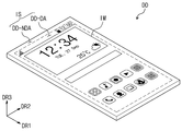
도 2a 및 도 2b는 각각 도 1에 도시된 표시 장치를 폴딩한 것을 도시한 것이다.
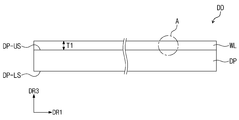
도 3은 본 발명의 일 실시예에 따른 표시 장치의 개략적인 단면도이다.
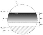
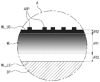
도 4는 도 3의 A 부분을 확대한 단면도이다.
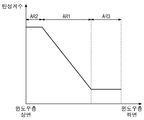
도 5는 본 발명의 일 실시예에 따른 표시 장치에 포함되는 윈도우 코팅층의 영역별 탄성 계수 관계를 나타낸 그래프이다.
도 6은 도 3의 A 부분을 확대한 단면도이다.
도 7은 본 발명의 일 실시예에 따른 표시 장치의 개략적인 단면도이다.
도 8a 내지 도 8d는 각각 본 발명의 일 실시예에 따른 표시 장치의 개략적인 단면도이다.
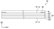
도 9는 본 발명의 일 실시예에 따른 표시 장치의 사시도이다.
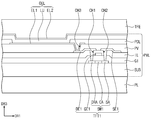
도 10은 본 발명의 일 실시예에 따른 표시 장치에 포함되는 화소들 중 하나의 회로도이다.
도 11은 도 10에 따른 회로도 일부의 개략적인 단면도이다.
도 12는 본 발명의 일 실시예에 따른 표시 장치의 개략적인 단면도이다.
DP-US: 표시 패널의 상면 DP-LS: 표시 패널의 하면
Claims (20)
- 표시 패널; 및
상기 표시 패널의 상면에 직접 배치되는 윈도우 코팅층을 포함하고,
상기 윈도우 코팅층은
상기 표시 패널에서 상기 윈도우 코팅층 방향으로 갈수록 탄성 계수가 증가하는 제1 영역을 포함하는 것인 표시 장치. - 제1항에 있어서,
상기 윈도우 코팅층은
2종 이상의 베이스 수지(resin)를 포함하는 것인 표시 장치. - 제1항에 있어서,
상기 윈도우 코팅층은
상기 제1 영역을 사이에 두고 서로 이격된 제2 영역 및 제3 영역을 포함하고,
상기 제2 영역 및 상기 제3 영역은 각각 일정한 탄성 계수를 갖는 표시 장치. - 제3항에 있어서,
상기 제2 영역은 상기 윈도우 코팅층의 상면을 포함하고,
상기 제3 영역은 상기 표시 패널의 상기 상면과 접촉하는 상기 윈도우 코팅층의 하면을 포함하며,
상기 제2 영역의 탄성 계수는 상기 제3 영역의 탄성 계수보다 큰 것인 표시 장치. - 제4항에 있어서,
상기 제2 영역의 탄성 계수는 1GPa 이상 10GPa 이하이고,
상기 제3 영역의 탄성 계수는 1MPa 이상 100MPa 이하인 것인 표시 장치. - 제4항에 있어서,
상기 제2 영역의 두께는 5㎛ 이상 20㎛ 이하인 것인 표시 장치. - 제1항에 있어서,
상기 윈도우 코팅층의 두께는 50㎛ 이상 1mm 이하인 것인 표시 장치. - 제7항에 있어서,
상기 윈도우 코팅층의 두께는 100㎛ 이상 500㎛ 이하인 것인 표시 장치. - 제1항에 있어서,
상기 윈도우 코팅층은 단일층 구조를 갖는 것인 표시 장치. - 제1항에 있어서,
상기 윈도우 코팅층은
자외선 흡수제를 포함하는 것인 표시 장치. - 제1항에 있어서,
상기 윈도우 코팅층의 상면에 형성된 불규칙한 요철 패턴을 포함하는 것인 표시 장치. - 제1항에 있어서,
상기 표시 패널은
베이스층;
상기 베이스층 상에 배치되고, 영상을 표시하는 화소층;
상기 화소층 상에 배치되고, 외부로부터 인가된 입력을 감지하는 입력 센싱층; 및
상기 화소층 상에 배치되고, 외광이 반사되는 것을 방지하는 반사 방지층을 포함하고,
상기 윈도우 코팅층은
상기 입력 센싱층 및 상기 반사 방지층 중 최외층(outermost layer)의 상면에 직접 배치되는 것인 표시 장치. - 제1항에 있어서,
상기 표시 패널의 상기 상면에 직접 배치되고, 상기 윈도우 코팅층과 접촉하며, 상기 윈도우 코팅층의 컬(curl)을 방지하는 제1 컬 방지 패턴을 더 포함하는 것인 표시 장치. - 제13항에 있어서,
상기 제1 컬 방지 패턴은 상기 윈도우 코팅층에 의해 커버되는 것인 표시 장치. - 제1항에 있어서,
상기 표시 패널의 하면에 직접 배치된 베이스 코팅층을 더 포함하는 것인 표시 장치. - 제15항에 있어서,
상기 베이스 코팅층은
1종의 베이스 수지(resin)을 포함하는 것인 표시 장치. - 제1항에 있어서,
적어도 일부가 벤딩되는 제1 모드 또는 상기 벤딩이 펼쳐진 제2 모드로 동작하는 것인 표시 장치. - 표시 패널; 및
상기 표시 패널의 상면에 직접 배치되고, 단일층 구조를 갖는 윈도우 코팅층을 포함하고,
상기 윈도우 코팅층은 복수 개의 탄성 계수를 갖는 것인 표시 장치. - 제18항에 있어서,
상기 윈도우 코팅층은 표시 패널에서 윈도우 코팅층 방향으로 갈수록 탄성 계수가 증가하는 제1 영역을 포함하는 것인 표시 장치. - 제18항에 있어서,
상기 윈도우 코팅층은 2종 이상의 베이스 수지(resin)을 포함하는 것인 표시 장치.
Priority Applications (3)
| Application Number | Priority Date | Filing Date | Title |
|---|---|---|---|
| KR1020170024942A KR102587768B1 (ko) | 2017-02-24 | 2017-02-24 | 표시 장치 |
| US15/837,293 US10658615B2 (en) | 2017-02-24 | 2017-12-11 | Display device |
| CN201810127535.3A CN108510889B (zh) | 2017-02-24 | 2018-02-08 | 显示设备 |
Applications Claiming Priority (1)
| Application Number | Priority Date | Filing Date | Title |
|---|---|---|---|
| KR1020170024942A KR102587768B1 (ko) | 2017-02-24 | 2017-02-24 | 표시 장치 |
Publications (2)
| Publication Number | Publication Date |
|---|---|
| KR20180098445A true KR20180098445A (ko) | 2018-09-04 |
| KR102587768B1 KR102587768B1 (ko) | 2023-10-12 |
Family
ID=63246996
Family Applications (1)
| Application Number | Title | Priority Date | Filing Date |
|---|---|---|---|
| KR1020170024942A Active KR102587768B1 (ko) | 2017-02-24 | 2017-02-24 | 표시 장치 |
Country Status (3)
| Country | Link |
|---|---|
| US (1) | US10658615B2 (ko) |
| KR (1) | KR102587768B1 (ko) |
| CN (1) | CN108510889B (ko) |
Cited By (3)
| Publication number | Priority date | Publication date | Assignee | Title |
|---|---|---|---|---|
| KR20210150626A (ko) * | 2020-06-03 | 2021-12-13 | 삼성디스플레이 주식회사 | 윈도우 및 이를 포함하는 표시 장치 |
| US11978370B2 (en) | 2020-07-14 | 2024-05-07 | Lg Display Co., Ltd. | Cover window and flexible display device having the same |
| US12507574B2 (en) | 2022-06-10 | 2025-12-23 | Samsung Display Co., Ltd. | Display device and method for manufacturing the same |
Families Citing this family (15)
| Publication number | Priority date | Publication date | Assignee | Title |
|---|---|---|---|---|
| KR102568895B1 (ko) * | 2014-03-13 | 2023-08-21 | 가부시키가이샤 한도오따이 에네루기 켄큐쇼 | 전자 장치 |
| CN107331688B (zh) * | 2017-07-14 | 2019-01-22 | 京东方科技集团股份有限公司 | 显示面板及其制备方法 |
| JP6556812B2 (ja) * | 2017-11-28 | 2019-08-07 | Nissha株式会社 | ハードコート付フィルムタイプタッチセンサとこれを用いたフレキシブルディバイス |
| KR102840830B1 (ko) * | 2018-02-28 | 2025-08-01 | 다이니폰 인사츠 가부시키가이샤 | 광학 필름 및 화상 표시 장치 |
| KR102786570B1 (ko) * | 2018-10-31 | 2025-03-27 | 삼성디스플레이 주식회사 | 표시 장치 및 그 제조 방법 |
| KR102774295B1 (ko) * | 2019-09-18 | 2025-03-05 | 삼성디스플레이 주식회사 | 윈도우 및 이를 포함하는 표시 장치 |
| KR20210035382A (ko) * | 2019-09-23 | 2021-04-01 | 삼성디스플레이 주식회사 | 표시 장치 및 캐리어 패널 |
| US11609606B2 (en) * | 2019-10-14 | 2023-03-21 | Samsung Display Co., Ltd. | Display apparatus |
| CN110634410A (zh) * | 2019-10-21 | 2019-12-31 | 昆山国显光电有限公司 | 显示装置 |
| CN111028690B (zh) * | 2019-12-25 | 2021-10-22 | 霸州市云谷电子科技有限公司 | 显示屏及显示屏加工方法 |
| KR102788347B1 (ko) * | 2019-12-30 | 2025-03-27 | 엘지디스플레이 주식회사 | 블랙매트릭스의 뜯김이 방지된 표시장치 |
| US20210257582A1 (en) * | 2020-02-14 | 2021-08-19 | Samsung Display Co., Ltd. | Display device |
| KR20220030470A (ko) * | 2020-09-01 | 2022-03-11 | 삼성디스플레이 주식회사 | 폴더블 표시 장치 |
| KR20220075008A (ko) * | 2020-11-26 | 2022-06-07 | 삼성디스플레이 주식회사 | 표시 장치 및 표시 장치의 제조 방법 |
| CN114397753A (zh) * | 2022-01-10 | 2022-04-26 | 深圳市国华光电研究院 | 耐光性能良好的电润湿显示器件 |
Citations (4)
| Publication number | Priority date | Publication date | Assignee | Title |
|---|---|---|---|---|
| KR20130031703A (ko) * | 2011-09-21 | 2013-03-29 | 제일모직주식회사 | 복합시트 및 이를 포함하는 표시소자용 기판 |
| KR20150021167A (ko) * | 2013-08-19 | 2015-03-02 | 삼성디스플레이 주식회사 | 접이식 표시 장치 |
| KR20160020615A (ko) * | 2014-08-13 | 2016-02-24 | 에스케이이노베이션 주식회사 | 하드코팅층 형성용 조성물 |
| KR20170015825A (ko) * | 2015-07-31 | 2017-02-09 | 삼성에스디아이 주식회사 | 표시 장치용 윈도우 필름 및 이를 포함하는 플렉시블 디스플레이 장치 |
Family Cites Families (20)
| Publication number | Priority date | Publication date | Assignee | Title |
|---|---|---|---|---|
| US7341766B2 (en) * | 2005-07-29 | 2008-03-11 | Dai Nippon Printing Co., Ltd. | Gas barrier clear film, and display substrate and display using the same |
| KR20120112549A (ko) * | 2009-12-17 | 2012-10-11 | 쓰리엠 이노베이티브 프로퍼티즈 컴파니 | 디스플레이 패널 어셈블리 및 이의 제조 방법 |
| JP5772598B2 (ja) * | 2009-12-25 | 2015-09-02 | 旭硝子株式会社 | ハードコート被膜付き樹脂基板およびその製造方法 |
| KR101476893B1 (ko) * | 2012-11-29 | 2014-12-26 | 삼성디스플레이 주식회사 | 플렉시블 디스플레이용 스크래치 방지 필름 |
| US9051493B2 (en) | 2013-03-28 | 2015-06-09 | Nokia Technologies Oy | Method and apparatus for joining together multiple functional layers of a flexible display |
| KR101773651B1 (ko) * | 2013-04-09 | 2017-08-31 | 주식회사 엘지화학 | 적층체 및 이를 이용하여 제조된 기판을 포함하는 소자 |
| KR20140124078A (ko) | 2013-04-15 | 2014-10-24 | 삼성디스플레이 주식회사 | 표시장치용 윈도우 및 이를 포함하는 표시 장치 |
| KR102080011B1 (ko) * | 2013-06-13 | 2020-02-24 | 삼성디스플레이 주식회사 | 표시장치 및 그 제조방법 |
| JP6167712B2 (ja) | 2013-07-16 | 2017-07-26 | 三菱ケミカル株式会社 | 耐擦傷性樹脂積層体 |
| KR102053226B1 (ko) | 2013-07-16 | 2019-12-06 | 엘지이노텍 주식회사 | 터치 윈도우 |
| KR20150035642A (ko) | 2013-09-27 | 2015-04-07 | 삼성디스플레이 주식회사 | 표시 장치용 윈도우 패널 및 이를 포함하는 표시 장치 |
| CN105940461B (zh) * | 2014-02-05 | 2018-06-15 | 国立研究开发法人科学技术振兴机构 | 伸缩性导电体及其制造方法和伸缩性导电体形成用糊料 |
| KR102267708B1 (ko) * | 2014-04-04 | 2021-06-23 | 삼성디스플레이 주식회사 | 표시장치 |
| KR20160028174A (ko) * | 2014-09-03 | 2016-03-11 | 삼성전자주식회사 | 코팅유닛 및 이를 갖는 전자기기 |
| KR101667658B1 (ko) * | 2014-12-30 | 2016-10-19 | 코오롱글로텍주식회사 | 플렉서블 전도성 패브릭 기판 및 그의 제조방법 |
| KR102425001B1 (ko) * | 2015-01-15 | 2022-07-25 | 삼성디스플레이 주식회사 | 가요성 윈도우, 이의 제작 방법 및 이를 이용한 플렉서블 디스플레이 |
| KR102345978B1 (ko) | 2015-01-16 | 2021-12-31 | 삼성디스플레이 주식회사 | 유기 발광 표시 장치 |
| KR102367252B1 (ko) * | 2015-04-16 | 2022-02-25 | 삼성디스플레이 주식회사 | 표시 장치 |
| KR102399568B1 (ko) * | 2015-09-23 | 2022-05-19 | 삼성디스플레이 주식회사 | 폴딩 가능한 디스플레이 장치 및 그 제조방법 |
| US10476037B2 (en) * | 2016-04-22 | 2019-11-12 | Samsung Sdi Co., Ltd. | Flexible display apparatus |
-
2017
- 2017-02-24 KR KR1020170024942A patent/KR102587768B1/ko active Active
- 2017-12-11 US US15/837,293 patent/US10658615B2/en active Active
-
2018
- 2018-02-08 CN CN201810127535.3A patent/CN108510889B/zh active Active
Patent Citations (4)
| Publication number | Priority date | Publication date | Assignee | Title |
|---|---|---|---|---|
| KR20130031703A (ko) * | 2011-09-21 | 2013-03-29 | 제일모직주식회사 | 복합시트 및 이를 포함하는 표시소자용 기판 |
| KR20150021167A (ko) * | 2013-08-19 | 2015-03-02 | 삼성디스플레이 주식회사 | 접이식 표시 장치 |
| KR20160020615A (ko) * | 2014-08-13 | 2016-02-24 | 에스케이이노베이션 주식회사 | 하드코팅층 형성용 조성물 |
| KR20170015825A (ko) * | 2015-07-31 | 2017-02-09 | 삼성에스디아이 주식회사 | 표시 장치용 윈도우 필름 및 이를 포함하는 플렉시블 디스플레이 장치 |
Cited By (4)
| Publication number | Priority date | Publication date | Assignee | Title |
|---|---|---|---|---|
| KR20210150626A (ko) * | 2020-06-03 | 2021-12-13 | 삼성디스플레이 주식회사 | 윈도우 및 이를 포함하는 표시 장치 |
| US12036767B2 (en) | 2020-06-03 | 2024-07-16 | Samsung Display Co., Ltd. | Window and display device including the same |
| US11978370B2 (en) | 2020-07-14 | 2024-05-07 | Lg Display Co., Ltd. | Cover window and flexible display device having the same |
| US12507574B2 (en) | 2022-06-10 | 2025-12-23 | Samsung Display Co., Ltd. | Display device and method for manufacturing the same |
Also Published As
| Publication number | Publication date |
|---|---|
| KR102587768B1 (ko) | 2023-10-12 |
| CN108510889B (zh) | 2021-10-08 |
| CN108510889A (zh) | 2018-09-07 |
| US10658615B2 (en) | 2020-05-19 |
| US20180248150A1 (en) | 2018-08-30 |
Similar Documents
| Publication | Publication Date | Title |
|---|---|---|
| KR102587768B1 (ko) | 표시 장치 | |
| US12029064B2 (en) | Foldable, flexible display apparatus and method of manufacturing the same | |
| US11495760B2 (en) | Display device and method for manufacturing display device | |
| US10916592B2 (en) | Organic light-emitting diode display device | |
| US9921414B2 (en) | Display device | |
| US10261546B2 (en) | Display device | |
| KR102554290B1 (ko) | 표시 장치 | |
| US11221648B2 (en) | Foldable display device | |
| KR20180021299A (ko) | 플렉서블 표시 장치 | |
| US11775008B2 (en) | Foldable display device | |
| CN106354296B (zh) | 显示设备 | |
| US11557740B2 (en) | Display device including adhesive layer having multiple adhesive layers | |
| KR20200140450A (ko) | 보호 윈도우를 포함하는 표시 장치 | |
| US12096660B2 (en) | Foldable display apparatus | |
| US20230041968A1 (en) | Cover window and display apparatus having the same | |
| CN223219446U (zh) | 显示设备 | |
| KR20240144710A (ko) | 표시 장치 및 표시 장치의 제조 방법 |
Legal Events
| Date | Code | Title | Description |
|---|---|---|---|
| PA0109 | Patent application |
Patent event code: PA01091R01D Comment text: Patent Application Patent event date: 20170224 |
|
| PG1501 | Laying open of application | ||
| A201 | Request for examination | ||
| PA0201 | Request for examination |
Patent event code: PA02012R01D Patent event date: 20220105 Comment text: Request for Examination of Application Patent event code: PA02011R01I Patent event date: 20170224 Comment text: Patent Application |
|
| E902 | Notification of reason for refusal | ||
| PE0902 | Notice of grounds for rejection |
Comment text: Notification of reason for refusal Patent event date: 20230426 Patent event code: PE09021S01D |
|
| E701 | Decision to grant or registration of patent right | ||
| PE0701 | Decision of registration |
Patent event code: PE07011S01D Comment text: Decision to Grant Registration Patent event date: 20230711 |
|
| GRNT | Written decision to grant | ||
| PR0701 | Registration of establishment |
Comment text: Registration of Establishment Patent event date: 20231005 Patent event code: PR07011E01D |
|
| PR1002 | Payment of registration fee |
Payment date: 20231006 End annual number: 3 Start annual number: 1 |
|
| PG1601 | Publication of registration |