KR20180098445A - Display device - Google Patents
Display device Download PDFInfo
- Publication number
- KR20180098445A KR20180098445A KR1020170024942A KR20170024942A KR20180098445A KR 20180098445 A KR20180098445 A KR 20180098445A KR 1020170024942 A KR1020170024942 A KR 1020170024942A KR 20170024942 A KR20170024942 A KR 20170024942A KR 20180098445 A KR20180098445 A KR 20180098445A
- Authority
- KR
- South Korea
- Prior art keywords
- layer
- coating layer
- window coating
- region
- display panel
- Prior art date
- Legal status (The legal status is an assumption and is not a legal conclusion. Google has not performed a legal analysis and makes no representation as to the accuracy of the status listed.)
- Granted
Links
Images


Classifications
-
- H—ELECTRICITY
- H10—SEMICONDUCTOR DEVICES; ELECTRIC SOLID-STATE DEVICES NOT OTHERWISE PROVIDED FOR
- H10K—ORGANIC ELECTRIC SOLID-STATE DEVICES
- H10K59/00—Integrated devices, or assemblies of multiple devices, comprising at least one organic light-emitting element covered by group H10K50/00
- H10K59/40—OLEDs integrated with touch screens
-
- G—PHYSICS
- G09—EDUCATION; CRYPTOGRAPHY; DISPLAY; ADVERTISING; SEALS
- G09F—DISPLAYING; ADVERTISING; SIGNS; LABELS OR NAME-PLATES; SEALS
- G09F9/00—Indicating arrangements for variable information in which the information is built-up on a support by selection or combination of individual elements
- G09F9/30—Indicating arrangements for variable information in which the information is built-up on a support by selection or combination of individual elements in which the desired character or characters are formed by combining individual elements
- G09F9/301—Indicating arrangements for variable information in which the information is built-up on a support by selection or combination of individual elements in which the desired character or characters are formed by combining individual elements flexible foldable or roll-able electronic displays, e.g. thin LCD, OLED
-
- G—PHYSICS
- G02—OPTICS
- G02B—OPTICAL ELEMENTS, SYSTEMS OR APPARATUS
- G02B1/00—Optical elements characterised by the material of which they are made; Optical coatings for optical elements
- G02B1/10—Optical coatings produced by application to, or surface treatment of, optical elements
-
- G—PHYSICS
- G02—OPTICS
- G02B—OPTICAL ELEMENTS, SYSTEMS OR APPARATUS
- G02B1/00—Optical elements characterised by the material of which they are made; Optical coatings for optical elements
- G02B1/04—Optical elements characterised by the material of which they are made; Optical coatings for optical elements made of organic materials, e.g. plastics
-
- G—PHYSICS
- G02—OPTICS
- G02B—OPTICAL ELEMENTS, SYSTEMS OR APPARATUS
- G02B6/00—Light guides; Structural details of arrangements comprising light guides and other optical elements, e.g. couplings
- G02B6/24—Coupling light guides
- G02B6/26—Optical coupling means
- G02B6/32—Optical coupling means having lens focusing means positioned between opposed fibre ends
- G02B6/325—Optical coupling means having lens focusing means positioned between opposed fibre ends comprising a transparent member, e.g. window, protective plate
-
- H01L27/323—
-
- H01L27/3244—
-
- H—ELECTRICITY
- H10—SEMICONDUCTOR DEVICES; ELECTRIC SOLID-STATE DEVICES NOT OTHERWISE PROVIDED FOR
- H10K—ORGANIC ELECTRIC SOLID-STATE DEVICES
- H10K50/00—Organic light-emitting devices
- H10K50/80—Constructional details
- H10K50/84—Passivation; Containers; Encapsulations
- H10K50/844—Encapsulations
-
- H—ELECTRICITY
- H10—SEMICONDUCTOR DEVICES; ELECTRIC SOLID-STATE DEVICES NOT OTHERWISE PROVIDED FOR
- H10K—ORGANIC ELECTRIC SOLID-STATE DEVICES
- H10K50/00—Organic light-emitting devices
- H10K50/80—Constructional details
- H10K50/86—Arrangements for improving contrast, e.g. preventing reflection of ambient light
- H10K50/865—Arrangements for improving contrast, e.g. preventing reflection of ambient light comprising light absorbing layers, e.g. light-blocking layers
-
- H—ELECTRICITY
- H10—SEMICONDUCTOR DEVICES; ELECTRIC SOLID-STATE DEVICES NOT OTHERWISE PROVIDED FOR
- H10K—ORGANIC ELECTRIC SOLID-STATE DEVICES
- H10K59/00—Integrated devices, or assemblies of multiple devices, comprising at least one organic light-emitting element covered by group H10K50/00
- H10K59/10—OLED displays
- H10K59/12—Active-matrix OLED [AMOLED] displays
-
- H—ELECTRICITY
- H10—SEMICONDUCTOR DEVICES; ELECTRIC SOLID-STATE DEVICES NOT OTHERWISE PROVIDED FOR
- H10K—ORGANIC ELECTRIC SOLID-STATE DEVICES
- H10K59/00—Integrated devices, or assemblies of multiple devices, comprising at least one organic light-emitting element covered by group H10K50/00
- H10K59/80—Constructional details
- H10K59/87—Passivation; Containers; Encapsulations
- H10K59/873—Encapsulations
-
- H—ELECTRICITY
- H10—SEMICONDUCTOR DEVICES; ELECTRIC SOLID-STATE DEVICES NOT OTHERWISE PROVIDED FOR
- H10K—ORGANIC ELECTRIC SOLID-STATE DEVICES
- H10K59/00—Integrated devices, or assemblies of multiple devices, comprising at least one organic light-emitting element covered by group H10K50/00
- H10K59/80—Constructional details
- H10K59/8791—Arrangements for improving contrast, e.g. preventing reflection of ambient light
- H10K59/8792—Arrangements for improving contrast, e.g. preventing reflection of ambient light comprising light absorbing layers, e.g. black layers
-
- H—ELECTRICITY
- H10—SEMICONDUCTOR DEVICES; ELECTRIC SOLID-STATE DEVICES NOT OTHERWISE PROVIDED FOR
- H10K—ORGANIC ELECTRIC SOLID-STATE DEVICES
- H10K2102/00—Constructional details relating to the organic devices covered by this subclass
- H10K2102/301—Details of OLEDs
- H10K2102/311—Flexible OLED
-
- H—ELECTRICITY
- H10—SEMICONDUCTOR DEVICES; ELECTRIC SOLID-STATE DEVICES NOT OTHERWISE PROVIDED FOR
- H10K—ORGANIC ELECTRIC SOLID-STATE DEVICES
- H10K2102/00—Constructional details relating to the organic devices covered by this subclass
- H10K2102/301—Details of OLEDs
- H10K2102/351—Thickness
-
- H—ELECTRICITY
- H10—SEMICONDUCTOR DEVICES; ELECTRIC SOLID-STATE DEVICES NOT OTHERWISE PROVIDED FOR
- H10K—ORGANIC ELECTRIC SOLID-STATE DEVICES
- H10K59/00—Integrated devices, or assemblies of multiple devices, comprising at least one organic light-emitting element covered by group H10K50/00
- H10K59/10—OLED displays
- H10K59/12—Active-matrix OLED [AMOLED] displays
- H10K59/131—Interconnections, e.g. wiring lines or terminals
Landscapes
- Physics & Mathematics (AREA)
- Optics & Photonics (AREA)
- General Physics & Mathematics (AREA)
- Engineering & Computer Science (AREA)
- Devices For Indicating Variable Information By Combining Individual Elements (AREA)
- Microelectronics & Electronic Packaging (AREA)
- Theoretical Computer Science (AREA)
- Electroluminescent Light Sources (AREA)
Abstract
본 명세서는 표시 장치에 관한 것이다. 표시 장치는 표시 패널, 표시 패널의 상면에 직접 배치되는 윈도우 코팅층을 포함한다. 윈도우 코팅층은 표시 패널에서 윈도우 코팅층 방향으로 갈수록 탄성 계수가 증가하는 제1 영역을 포함한다.This specification relates to a display device. The display device includes a display panel and a window coating layer disposed directly on the upper surface of the display panel. The window coating layer includes a first region where the elastic modulus increases from the display panel toward the window coating layer.
Description
본 발명은 표시 장치에 관한 것으로, 보다 상세하게는 표시 패널 상면에 직접 배치되는 윈도우 코팅층을 포함하는 표시 장치에 관한 것이다.The present invention relates to a display device, and more particularly, to a display device including a window coating layer disposed directly on an upper surface of a display panel.
최근 정보 디스플레이에 관한 관심이 고조되고 휴대가 가능한 정보매체를 이용하려는 요구가 높아지면서 기존의 표시소자인 브라운관(Cathode Ray Tube; CRT)을 대체하는 경량 박형 평판표시소자(Flat Panel Display; FPD)에 대한 연구 및 상업화가 중점적으로 이루어지고 있다.In recent years, there has been a growing interest in information display and a demand for a portable information medium has increased, and a lightweight flat panel display (FPD) that replaces a cathode ray tube (CRT) And research and commercialization are being carried out.
표시 장치는 표시화면에 다양한 이미지를 표시하여 사용자에게 정보를 제공한다. 최근 벤딩(bending) 가능한 표시 장치가 개발되고 있다. 플렉서블 표시 장치는 평판 표시 장치와 달리, 종이처럼 접거나 말거나 휠 수 있다. 형상이 다양하게 변경될 수 있는 플렉서블 표시 장치는 휴대가 용이하고 사용자의 편의성을 향상시킬 수 있다. 플렉서블 표시 장치는 롤러블 표시 장치, 폴더블 표시 장치 등으로 구분될 수 있다.The display device displays various images on the display screen to provide information to the user. Recently, a display device capable of bending is being developed. Unlike flat panel display devices, flexible display devices can be folded or rolled like paper. The flexible display device whose shape can be changed variously is easy to carry and can improve the convenience of the user. The flexible display device can be classified into a rollable display device, a foldable display device, and the like.
본 발명의 일 목적은 내구성이 우수함과 동시에 벤딩 시 박리 문제를 개선할 수 있는 윈도우 코팅층이 적용된 표시 장치를 제공하는 것이다.It is an object of the present invention to provide a display device to which a window coating layer is applied, which is excellent in durability and can improve a peeling-off problem in bending.
본 발명의 일 실시예는 표시 패널, 및 표시 패널의 상면에 직접 배치되는 윈도우 코팅층을 포함하고, 윈도우 코팅층은 표시 패널에서 윈도우 코팅층 방향으로 갈수록 탄성 계수가 증가하는 제1 영역을 포함하는 것인 표시 장치를 제공한다.An embodiment of the present invention includes a display panel and a window coating layer disposed directly on an upper surface of the display panel, wherein the window coating layer includes a first area where the elastic coefficient increases from the display panel toward the window coating layer Device.
윈도우 코팅층은 2종 이상의 베이스 수지(resin)를 포함하는 것일 수 있다.The window coating layer may comprise two or more base resins.
윈도우 코팅층은 제1 영역을 사이에 두고 서로 이격된 제2 영역 및 제3 영역을 포함하고, 제2 영역 및 제3 영역은 각각 일정한 탄성 계수를 갖는 것일 수 있다.The window coating layer may include a second region and a third region that are spaced apart from each other with a first region interposed therebetween, and the second region and the third region may each have a constant elastic modulus.
제2 영역의 탄성 계수는 1GPa 이상 10GPa 이하이고, 제3 영역의 탄성 계수는 1MPa 이상 100MPa 이하인 것일 수 있다.The elastic modulus of the second region may be 1 GPa or more and 10 GPa or less, and the elastic modulus of the third region may be 1 MPa or more and 100 MPa or less.
제2 영역의 두께는 5㎛ 이상 20㎛ 이하인 것일 수 있다. The thickness of the second region may be 5 탆 or more and 20 탆 or less.
윈도우 코팅층의 두께는 50㎛ 이상 1mm 이하인 것일 수 있고, 구체적으로, 100㎛ 이상 500㎛ 이하인 것일 수 있다.The thickness of the window coating layer may be 50 占 퐉 or more and 1 mm or less, specifically 100 占 퐉 or more and 500 占 퐉 or less.
윈도우 코팅층은 단일층 구조를 갖는 것일 수 있다.The window coating layer may have a single layer structure.
윈도우 코팅층은 자외선 흡수제를 포함하는 것일 수 있다.The window coating layer may comprise an ultraviolet absorber.
윈도우 코팅층의 상면에 형성된 불규칙한 요철 패턴을 포함하는 것일 수 있다.And an irregular concavo-convex pattern formed on the upper surface of the window coating layer.
표시 패널은 베이스층, 베이스층 상에 배치되고 영상을 표시하는 화소층, 화소층 상에 배치되고 외부로부터 인가된 입력을 감지하는 입력 센싱층, 및 화소층 상에 배치되고 외광이 반사되는 것을 방지하는 반사 방지층을 포함하고, 윈도우 코팅층은 입력 센싱층 및 반사 방지층 중 최외층(outermost layer)의 상면에 직접 배치되는 것일 수 있다.The display panel includes a base layer, a pixel layer disposed on the base layer and displaying an image, an input sensing layer disposed on the pixel layer and sensing an externally applied input, and an input sensing layer disposed on the pixel layer, And the window coating layer may be disposed directly on the upper surface of the outermost layer of the input sensing layer and the antireflective layer.
표시 장치는 표시 패널의 상면에 직접 배치되고, 윈도우 코팅층과 접촉하며, 윈도우 코팅층의 컬(curl)을 방지하는 제1 컬 방지 패턴을 더 포함하는 것일 수 있다.The display device may further comprise a first curl preventing pattern disposed directly on the upper surface of the display panel and in contact with the window coating layer and preventing curling of the window coating layer.
제1 컬 방지 패턴은 윈도우 코팅층에 의해 커버되는 것일 수 있다.The first anti-curl pattern may be covered by a window coating layer.
표시 장치는 표시 패널의 하면에 직접 배치된 베이스 코팅층을 더 포함하는 것일 수 있다.The display device may further comprise a base coating layer disposed directly on the lower surface of the display panel.
베이스 코팅층은 1종의 베이스 수지(resin)을 포함하는 것일 수 있다.The base coating layer may comprise one kind of base resin.
표시 장치는 적어도 일부가 벤딩되는 제1 모드 또는 벤딩이 펼쳐진 제2 모드로 동작하는 것일 수 있다.The display device may be operated in a first mode in which at least a part is bent or in a second mode in which the bending is opened.
본 발명의 일 실시예는 표시 패널 및 표시 패널의 상면에 직접 배치되고 단일층 구조를 갖는 윈도우 코팅층을 포함하고, 윈도우 코팅층은 복수 개의 탄성 계수를 갖는 것일 수 있다.One embodiment of the present invention may include a display panel and a window coating layer disposed directly on the upper surface of the display panel and having a single layer structure, and the window coating layer may have a plurality of elastic moduli.
윈도우 코팅층은 표시 패널에서 윈도우 코팅층 방향으로 갈수록 탄성 계수가 증가하는 제1 영역을 포함하는 것일 수 있다.The window coating layer may include a first region where the elastic modulus increases from the display panel toward the window coating layer.
윈도우 코팅층은 2종 이상의 베이스 수지(resin)을 포함하는 것일 수 있다.The window coating layer may comprise two or more base resins.
본 발명의 일 실시예에 따른 표시 장치는 점착 부재 없이 표시 패널 상면에 윈도우 코팅층을 직접 배치시킨 구조를 포함하며, 윈도우 코팅층이 탄성 계수 구배를 갖는 영역을 포함함으로써 내구성이 우수함과 동시에 벤딩 시 박리 문제를 최소화할 수 있다.A display device according to an embodiment of the present invention includes a structure in which a window coating layer is directly disposed on a top surface of a display panel without an adhesive member and the window coating layer includes a region having a modulus of elastic modulus to thereby exhibit excellent durability, Can be minimized.
도 1은 본 발명의 일 실시예에 따른 표시 장치의 사시도이다.
도 2a 및 도 2b는 각각 도 1에 도시된 표시 장치를 폴딩한 것을 도시한 것이다.
도 3은 본 발명의 일 실시예에 따른 표시 장치의 개략적인 단면도이다.
도 4는 도 3의 A 부분을 확대한 단면도이다.
도 5는 본 발명의 일 실시예에 따른 표시 장치에 포함되는 윈도우 코팅층의 영역별 탄성 계수 관계를 나타낸 그래프이다.
도 6은 도 3의 A 부분을 확대한 단면도이다.
도 7은 본 발명의 일 실시예에 따른 표시 장치의 개략적인 단면도이다.
도 8a 내지 도 8d는 각각 본 발명의 일 실시예에 따른 표시 장치의 개략적인 단면도이다.
도 9는 본 발명의 일 실시예에 따른 표시 장치의 사시도이다.
도 10은 본 발명의 일 실시예에 따른 표시 장치에 포함되는 화소들 중 하나의 회로도이다.
도 11은 도 10에 따른 회로도 일부의 개략적인 단면도이다.
도 12는 본 발명의 일 실시예에 따른 표시 장치의 개략적인 단면도이다.1 is a perspective view of a display device according to an embodiment of the present invention.
Figs. 2A and 2B each show a folding of the display device shown in Fig. 1. Fig.
3 is a schematic cross-sectional view of a display device according to an embodiment of the present invention.
4 is an enlarged cross-sectional view of a portion A in Fig.
FIG. 5 is a graph illustrating a relationship between elastic modulus of a window coating layer included in a display device according to an exemplary embodiment of the present invention.
6 is an enlarged cross-sectional view of portion A of Fig.
7 is a schematic cross-sectional view of a display device according to an embodiment of the present invention.
8A to 8D are schematic cross-sectional views of a display device according to an embodiment of the present invention.
9 is a perspective view of a display device according to an embodiment of the present invention.
10 is a circuit diagram of one of the pixels included in the display device according to the embodiment of the present invention.
11 is a schematic cross-sectional view of a portion of the circuit diagram according to Fig.
12 is a schematic cross-sectional view of a display device according to an embodiment of the present invention.
이상의 본 발명의 목적들, 다른 목적들, 특징들 및 이점들은 첨부된 도면과 관련된 이하의 바람직한 실시예들을 통해서 쉽게 이해될 것이다. 그러나 본 발명은 여기서 설명되는 실시예들에 한정되지 않고 다른 형태로 구체화될 수도 있다. 오히려, 여기서 소개되는 실시예들은 개시된 내용이 철저하고 완전해질 수 있도록 그리고 통상의 기술자에게 본 발명의 사상이 충분히 전달될 수 있도록 하기 위해 제공되는 것이다.BRIEF DESCRIPTION OF THE DRAWINGS The above and other objects, features, and advantages of the present invention will become more readily apparent from the following description of preferred embodiments with reference to the accompanying drawings. However, the present invention is not limited to the embodiments described herein but may be embodied in other forms. Rather, the embodiments disclosed herein are provided so that this disclosure will be thorough and complete, and will fully convey the concept of the invention to those skilled in the art.
각 도면을 설명하면서 유사한 참조부호를 유사한 구성요소에 대해 사용하였다. 첨부된 도면에 있어서, 구조물들의 치수는 본 발명의 명확성을 위하여 실제보다 확대하여 도시한 것이다. 제1, 제2 등의 용어는 다양한 구성요소들을 설명하는데 사용될 수 있지만, 상기 구성요소들은 상기 용어들에 의해 한정되어서는 안 된다. 상기 용어들은 하나의 구성요소를 다른 구성요소로부터 구별하는 목적으로만 사용된다. 예를 들어, 본 발명의 권리 범위를 벗어나지 않으면서 제1 구성요소는 제2 구성요소로 명명될 수 있고, 유사하게 제2 구성요소도 제1 구성요소로 명명될 수 있다. 단수의 표현은 문맥상 명백하게 다르게 뜻하지 않는 한, 복수의 표현을 포함한다.Like reference numerals are used for like elements in describing each drawing. In the accompanying drawings, the dimensions of the structures are shown enlarged from the actual for the sake of clarity of the present invention. The terms first, second, etc. may be used to describe various components, but the components should not be limited by the terms. The terms are used only for the purpose of distinguishing one component from another. For example, without departing from the scope of the present invention, the first component may be referred to as a second component, and similarly, the second component may also be referred to as a first component. The singular expressions include plural expressions unless the context clearly dictates otherwise.
본 출원에서, "포함하다" 또는 "가지다" 등의 용어는 명세서 상에 기재된 특징, 숫자, 단계, 동작, 구성요소, 부품 또는 이들을 조합한 것이 존재함을 지정하려는 것이지, 하나 또는 그 이상의 다른 특징들이나 숫자, 단계, 동작, 구성요소, 부분품 또는 이들을 조합한 것들의 존재 또는 부가 가능성을 미리 배제하지 않는 것으로 이해되어야 한다. 또한, 층, 막, 영역, 판 등의 부분이 다른 부분 "상에" 있다고 할 경우, 이는 다른 부분 "바로 위에" 있는 경우뿐만 아니라 그 중간에 또 다른 부분이 있는 경우도 포함한다. 반대로 층, 막, 영역, 판 등의 부분이 다른 부분 "하부에" 있다고 할 경우, 이는 다른 부분 "바로 아래에" 있는 경우뿐만 아니라 그 중간에 또 다른 부분이 있는 경우도 포함한다.In the present application, the terms "comprises" or "having" and the like are used to specify that there is a feature, a number, a step, an operation, an element, a component or a combination thereof described in the specification, But do not preclude the presence or addition of one or more other features, integers, steps, operations, components, parts, or combinations thereof. Also, where a portion such as a layer, film, region, plate, or the like is referred to as being "on" another portion, this includes not only the case where it is "directly on" another portion, but also the case where there is another portion in between. On the contrary, when a part such as a layer, film, region, plate or the like is referred to as being "under" another part, it includes not only the case where it is "directly underneath" another part but also another part in the middle.
이하, 본 발명의 일 실시예에 따른 표시 장치에 대하여 설명한다.Hereinafter, a display device according to an embodiment of the present invention will be described.
도 1은 본 발명의 일 실시예에 따른 표시 장치의 사시도이다.1 is a perspective view of a display device according to an embodiment of the present invention.
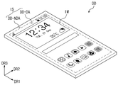
도 1을 참조하면, 본 발명의 일 실시예에 따른 표시 장치(DD)는 이미지(IM)가 표시되는 표시면(IS)을 포함하며, 표시면(IS)은 제1 방향축(DR1)과 제2 방향축(DR2)이 정의하는 면과 평행한다. 표시면(IS)의 법선 방향, 즉 표시 장치(DD)의 두께 방향은 제3 방향축(DR3)이 지시한다. 각 부재들의 상면(또는 전면)과 하면(또는 배면)은 제3 방향축(DR3)에 의해 구분된다. 그러나, 제1 내지 제3 방향축들(DR1, DR2, DR3)이 지시하는 방향은 상대적인 개념으로서 다른 방향으로 변환될 수 있다. 이하, 제1 내지 제3 방향들은 제1 내지 제3 방향축들(DR1, DR2, DR3)이 각각 지시하는 방향으로 동일한 도면 부호를 참조한다. 본 발명의 일 실시예에 따른 표시 장치(DD)는 플렉서블 표시 장치일 수 있다. 다만, 이에 의하여 한정되는 것은 아니며, 본 발명의 일 실시예에 따른 표시 장치(DD)는 리지드(rigid)한 표시 장치일 수도 있다.1, a display device DD according to an exemplary embodiment of the present invention includes a display surface IS on which an image IM is displayed, and a display surface IS includes a first directional axis DR1, And is parallel to the plane defined by the second directional axis DR2. The normal direction of the display surface IS, i.e., the thickness direction of the display device DD, is indicated by the third directional axis DR3. The upper surface (or the front surface) and the lower surface (or the back surface) of each of the members are separated by the third direction axis DR3. However, the directions indicated by the first to third direction axes DR1, DR2, DR3 can be converted into different directions as relative concepts. Hereinafter, the first to third directions refer to the same reference numerals in the directions indicated by the first to third direction axes DR1, DR2, and DR3, respectively. The display device DD according to an embodiment of the present invention may be a flexible display device. However, the present invention is not limited thereto, and the display device DD according to an embodiment of the present invention may be a rigid display device.
본 발명의 일 실시예에 따른 표시 장치(DD)는 폴더블 표시 장치 또는 말려지는 롤러블 표시 장치일 수 있고, 특별히 제한되지 않는다. 본 발명의 일 실시예에 따른 표시 장치(DD)는 텔레비전, 모니터 등과 같은 대형 전자장치를 비롯하여, 휴대 전화, 테블릿, 자동차 네비게이션, 게임기, 스마트 와치 등과 같은 중소형 전자장치 등에 사용될 수 있다.The display device DD according to an embodiment of the present invention may be a foldable display device or a rolled-up display device, and is not particularly limited. The display device DD according to an exemplary embodiment of the present invention can be used for a large-sized electronic device such as a television, a monitor, etc., and a small-sized electronic device such as a cellular phone, a tablet, a car navigation system, a game machine,
도 1에 도시된 것과 같이, 표시 장치(DD)의 표시면(IS)은 복수 개의 영역들을 포함할 수 있다. 표시 장치(DD)는 이미지(IM)가 표시되는 표시 영역(DD-DA) 및 표시 영역(DD-DA)에 인접한 비표시 영역(DD-NDA)을 포함한다. 비표시 영역(DD-NDA)은 이미지가 표시되지 않는 영역이다. 도 1에는 이미지(IM)의 일 예로 어플리케이션의 아이콘들과 시계창을 도시하였다. 표시 영역(DD-DA)은 사각형상일 수 있다. 비표시 영역(DD-NDA)은 표시 영역(DD-DA)을 에워싸을 수 있다. 다만, 이에 제한되지 않고, 표시 영역(DD-DA)의 형상과 비표시 영역(DD-NDA)의 형상은 상대적으로 디자인될 수 있다.As shown in Fig. 1, the display surface IS of the display device DD may include a plurality of areas. The display device DD includes a display area DD-DA in which the image IM is displayed and a non-display area DD-NDA adjacent to the display area DD-DA. The non-display area (DD-NDA) is an area where no image is displayed. FIG. 1 shows application icons and a clock window as an example of an image IM. The display area DD-DA may be rectangular in shape. The non-display area DD-NDA can surround the display area DD-DA. However, the shape of the display area DD-DA and the shape of the non-display area DD-NDA can be relatively designed, without being limited thereto.
본 발명의 일 실시예에 따른 표시 장치(DD)는 하우징(미도시)을 포함할 수 있다. 하우징(미도시)은 표시 장치(DD)의 외곽에 배치되며, 내부에 부품들을 수용할 수 있다.The display device DD according to an embodiment of the present invention may include a housing (not shown). The housing (not shown) is disposed at the outer periphery of the display device DD and can receive the components therein.
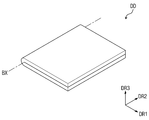
도 2a 및 도 2b는 각각 도 1에 도시된 표시 장치를 폴딩한 것을 도시한 것이다.Figs. 2A and 2B each show a folding of the display device shown in Fig. 1. Fig.
도 1, 도 2a 및 도 2b를 참조하면, 본 발명의 일 실시예에 따른 표시 장치(DD)는 적어도 일부가 벤딩되는 제1 모드 또는 벤딩이 펼쳐진 제2 모드로 동작하는 것일 수 있다. 도 2a 및 도 2b는 제1 모드로 동작하는 표시 장치(DD)를 예시적으로 도시한 것이고, 도 1은 제2 모드로 동작하는 표시 장치(DD)를 예시적으로 도시한 것이다. 도 2a를 참조하면, 제1 모드에서 본 발명의 일 실시예에 따른 표시 장치(DD)는 벤딩축(BX)을 기준으로 인-폴딩 될 수 있다. 다만, 이에 의하여 한정되는 것은 아니며, 도 2b를 참조하면, 제1 모드에서 본 발명의 일 실시예에 따른 표시 장치(DD)는 벤딩축(BX)을 기준으로 아웃-폴딩 될 수도 있다.Referring to FIGS. 1, 2A and 2B, a display device DD according to an exemplary embodiment of the present invention may be operated in a first mode in which at least a portion is bent or in a second mode in which a bent portion is opened. 2A and 2B illustrate a display device DD operating in a first mode, and Fig. 1 exemplarily shows a display device DD operating in a second mode. Referring to FIG. 2A, in a first mode, a display device DD according to an embodiment of the present invention may be in-fold with respect to a bending axis BX. Referring to FIG. 2B, in the first mode, the display device DD according to an exemplary embodiment of the present invention may be out-folded with respect to the bending axis BX.
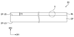
도 3은 본 발명의 일 실시예에 따른 표시 장치의 개략적인 단면도이다.3 is a schematic cross-sectional view of a display device according to an embodiment of the present invention.
도 3을 참조하면, 본 발명의 일 실시예에 따른 표시 장치(DD)는 표시 패널(DP) 및 윈도우 코팅층(WL)을 포함한다. 윈도우 코팅층(WL)은 표시 패널(DP)의 상면(DP-US)에 직접 배치된다. 즉, 윈도우 코팅층(WL)은 점착 부재의 개재없이 표시 패널(DP) 상에 배치된다.Referring to FIG. 3, a display device DD according to an embodiment of the present invention includes a display panel DP and a window coating layer WL. The window coating layer WL is disposed directly on the upper surface DP-US of the display panel DP. That is, the window coating layer WL is disposed on the display panel DP without interposing the adhesive member.
윈도우 코팅층(WL)이 점착 부재들 없이 표시 패널(DP)의 상면(DP-US)에 직접 배치됨으로써, 점착시 발생되는 눌림 현상 및 점착 부재의 크리프(creep) 특성에 의한 플렉서블 표시 장치의 복원성 저하를 방지할 수 있고, 나아가 공정을 단순화할 수 있어 플렉서블한 표시 장치를 용이하게 구현할 수 있다.Since the window coating layer WL is disposed directly on the upper surface DP-US of the display panel DP without the adhesive members, the pressing phenomenon occurring at the time of adhering and the creep characteristics of the adhesive member reduce the stability of the flexible display device It is possible to simplify the process and to easily implement a flexible display device.
이에 한정되는 것은 아니나, 윈도우 코팅층(WL)의 두께(T1)는 50㎛ 이상 1mm 이하일 수 있다. 윈도우 코팅층(WL)은 표시 패널(DP)을 보호하는 층으로 두께(T1)가 50㎛ 미만인 경우 경도, 내충격성, 내스크래치성 등의 내구성이 충분히 확보되지 못한다는 문제점이 있다. 윈도우 코팅층(WL)은 보호층 역할을 수행하기 위해 일정 수준 이상의 두께가 요구되나, 윈도우 코팅층(WL)의 두께(T1)가 1mm 초과일 경우, 헤이즈가 증가하거나, 표시 장치(DD)를 벤딩할 경우 원하는 작은 곡률 반경을 구현하기 어렵다는 문제점이 있다.Though not limited thereto, the thickness T1 of the window coating layer WL may be 50 占 퐉 or more and 1 mm or less. The window coating layer WL is a layer for protecting the display panel DP. When the thickness T1 is less than 50 탆, durability such as hardness, impact resistance and scratch resistance can not be sufficiently secured. When the thickness T1 of the window coating layer WL is more than 1 mm, the haze increases or the bending of the display device DD may occur. There is a problem that it is difficult to realize a desired small radius of curvature.
구체적으로, 윈도우 코팅층(WL)의 두께(T1)는 100㎛ 이상 500㎛ 이하인 것일 수 있고, 예를 들어, 윈도우 코팅층(WL)의 두께(T1)는 150㎛ 이상 250㎛ 이하, 또는 약 200㎛일 수 있다.For example, the thickness T1 of the window coating layer WL may be 150 占 퐉 or more and 250 占 퐉 or less, or about 200 占 퐉 or less. The thickness T1 of the window coating layer WL may be 100 占 퐉 or more and 500 占 퐉 or less. Lt; / RTI >
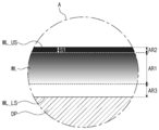
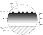
도 4는 도 3의 A 부분을 확대한 단면도이다.4 is an enlarged cross-sectional view of a portion A in Fig.
도 4를 참조하면, 윈도우 코팅층(WL)은 표시 패널(DP) 방향에서 윈도우 코팅층(WL) 방향으로 갈수록 탄성 계수가 증가하는 제1 영역(AR1)을 포함한다. 다시 말해, 윈도우 코팅층(WL)의 제1 영역(AR1)은 윈도우 코팅층(WL)의 하면(WL-LS)에서 상면(WL-US) 방향으로 갈수록 탄성 계수가 증가하는 영역이다. 도 4에서는 제1 영역(AR1)이 윈도우 코팅층(WL)의 일부에 대응하는 것을 예를 들어 도시하였으나 이에 한정되는 것은 아니며, 윈도우 코팅층(WL) 전체가 제1 영역(AR1)에 대응하는 것일 수 있다.Referring to FIG. 4, the window coating layer WL includes a first region AR1 whose elastic modulus increases from the display panel DP toward the window coating layer WL. In other words, the first area AR1 of the window coating layer WL is a region where the elastic modulus increases from the lower surface WL-LS to the upper surface WL-US of the window coating layer WL. In FIG. 4, the first area AR1 corresponds to a portion of the window coating layer WL. However, the present invention is not limited thereto, and the entire window coating layer WL may correspond to the first area AR1 have.
이에 한정되는 것은 아니나, 윈도우 코팅층(WL)의 상면(WL-US)은 표시 장치(DD)의 외부면을 정의하는 것일 수 있다.Although not limited thereto, the upper surface WL-US of the window coating layer WL may define the outer surface of the display device DD.
윈도우 코팅층(WL)이 상면(WL-US)으로 갈수록 탄성 계수가 증가하는 제1 영역(AR1)을 포함함으로써 윈도우 코팅층(WL)의 상측 영역은 표시 패널(DP)을 보호하는 역할을 효율적으로 수행할 수 있으며, 윈도우 코팅층(WL)의 하측 영역은 표시 패널(DP)의 상면(WL-LS)과의 탄성 계수 차이를 최소화하여 표시 장치(DD) 벤딩 시 표시 패널(DP)과 윈도우 코팅층(WL)이 박리되는 버클링(buckling) 발생률을 최소화할 수 있다.The upper area of the window coating layer WL effectively protects the display panel DP by including the first area AR1 where the elastic modulus increases as the window coating layer WL approaches the upper surface WL-US And the lower area of the window coating layer WL minimizes the difference in elastic modulus between the display panel DP and the upper surface WL-LS of the display panel DP, It is possible to minimize the buckling occurrence rate at which peeling occurs.
윈도우 코팅층(WL)은 탄성 계수 구배를 갖는 제1 영역(AR1)을 포함하기 위해, 2종 이상의 베이스 수지를 포함하는 것일 수 있다. "베이스 수지"는 윈도우 코팅층(WL)에 포함되는 재료 중 주요 성분이 되는 수지를 의미하는 것일 수 있다. 베이스 수지는 특별히 한정되는 것은 아니나 예를 들어, 열경화성 수지 재료를 포함하는 것일 수 있다. 예를 들어, 베이스 수지는 폴리우레탄계, 우레탄 아크릴레이트계, 폴리우레아계, 에폭시계, 실리콘계 등을 포함할 수 있다. 2종 이상의 베이스 수지는 동일한 계열의 수지를 포함하는 것일 수 있으며, 이 경우 측쇄 구조 등 구체적인 구조가 상이한 것일 수 있다. 2종 이상의 베이스 수지가 동일한 계열의 수지를 포함하는 경우, 혼합이 용이하게 될 수 있다는 장점이 있다. 다만, 이에 의하여 한정되는 것은 아니다.The window coating layer WL may comprise two or more base resins to include a first region AR1 having a modulus of elasticity modulus. The "base resin" may mean a resin that is a main component of the material contained in the window coating layer (WL). The base resin is not particularly limited, but may include, for example, a thermosetting resin material. For example, the base resin may include a polyurethane system, a urethane acrylate system, a polyurea system, an epoxy system, a silicone system, and the like. The two or more kinds of base resins may contain the same series of resins, and in this case, the specific structure such as the side chain structure may be different. If two or more base resins contain the same series of resins, there is an advantage that mixing can be facilitated. However, it is not limited thereto.
윈도우 코팅층(WL)은 예를 들어, 2종, 3종 또는 4종의 베이스 수지를 포함하는 것일 수 있다.The window coating layer WL may comprise, for example, two, three or four kinds of base resins.
윈도우 코팅층(WL)은 표시 패널(DP)의 상면(DP-US) 상에 코팅(coating), 프린팅(printing) 방식 등에 의해서 형성될 수 있다. 예를 들어, 윈도우 코팅층(WL)은 접착 부재들 없이 표시 패널(DP)의 상면(DP-US)에 롤코팅, 실크스크린 코팅, 스프레이 코팅, 슬릿 코팅 등에 의해 형성될 수 있다. 다만, 윈도우 코팅층(WL)이 표시 패널(DP)의 상면(DP-US)에 코팅되는 방식은 상기 열거한 방식들에 한정되지 않으며, 다양한 코팅 방법에 의해서 윈도우 코팅층(WL)은 표시 패널(DP)의 상면(DP-US)에 직접 코팅될 수 있다.The window coating layer WL may be formed on the upper surface DP-US of the display panel DP by a coating method, a printing method, or the like. For example, the window coating layer WL may be formed by roll coating, silk screen coating, spray coating, slit coating, etc. on the upper surface (DP-US) of the display panel DP without the adhesive members. However, the manner in which the window coating layer WL is coated on the upper surface DP-US of the display panel DP is not limited to the above-described schemes, and the window coating layer WL may be formed on the display panel DP (DP-US).
예를 들어, 표시 패널(DP)의 상면(DP-US) 상에 2종 이상의 베이스 수지를 포함하는 베이스 조성물을 도포하고 경화하는 방법을 통해 윈도우 코팅층(WL)이 형성될 수 있다. 베이스 조성물의 점도는 100cps 이상 10000cps 이하인 것일 수 있다. 베이스 조성물의 점도가 100cps 미만인 경우, 코팅 두께 유지가 어려우며, 베이스 조성물의 점도가 1000cps 초과인 경우, 2종 이상의 베이스 레진 간의 혼합이 느리게 진행되어 공정 효율 측면에서 불리하다. 베이스 조성물의 점도는 예를 들어, 1000cps 이상 5000cps일 수 있다.For example, a window coating layer WL may be formed by applying and curing a base composition comprising two or more base resins on an upper surface (DP-US) of a display panel (DP). The viscosity of the base composition may be 100 cps or more and 10000 cps or less. When the viscosity of the base composition is less than 100 cps, it is difficult to maintain the coating thickness, and when the viscosity of the base composition is more than 1000 cps, mixing between two or more base resins proceeds slowly, which is disadvantageous in terms of process efficiency. The viscosity of the base composition may be, for example, from 1000 cps to 5000 cps.
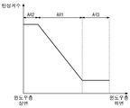
도 5는 본 발명의 일 실시예에 따른 표시 장치에 포함되는 윈도우 코팅층의 영역별 탄성 계수 관계를 나타낸 그래프이다.FIG. 5 is a graph illustrating a relationship between elastic modulus of a window coating layer included in a display device according to an exemplary embodiment of the present invention.
도 4 및 도 5를 참조하면, 윈도우 코팅층(WL)은 제1 영역(AR1)을 사이에 두고 제3 방향(DR3)으로 서로 이격된 제2 영역(AR2) 및 제3 영역(AR3)을 포함하는 것일 있다. 제2 영역(AR2) 및 제3 영역(AR3) 각각은 제1 영역(AR1)과 달리 일정한 탄성 계수를 갖는 것일 수 있다. 4 and 5, the window coating layer WL includes a second area AR2 and a third area AR3 that are spaced apart from each other in a third direction DR3 with the first area AR1 therebetween It is possible to do. Each of the second area AR2 and the third area AR3 may have a constant elastic modulus different from that of the first area AR1.
제2 영역(AR2)은 윈도우 코팅층(WL)의 상면(WL-US)을 포함하는 영역이고, 제3 영역(AR3)은 윈도우 코팅층(WL)의 하면(WL-LS)을 포함하는 영역일 수 있다. 윈도우 코팅층(WL)의 하면(WL-LS)은 표시 패널(DP)의 상면(예를 들어, 도 3의 DP-US)과 접촉하는 면이다.The second area AR2 is an area including the upper surface WL-US of the window coating layer WL and the third area AR3 is the area including the lower surface WL-LS of the window coating layer WL. have. The lower surface WL-LS of the window coating layer WL is a surface which contacts the upper surface (e.g., DP-US in Fig. 3) of the display panel DP.
윈도우 코팅층(WL)의 상면(WL-US)을 포함하는 제2 영역(AR2)은 외부 충격으로부터 표시 패널(DP)을 보호하는 역할을 수행하기 위한 내구성 확보가 요구되는 바, 윈도우 코팅층(WL)의 하면(WL-LS)을 포함하는 제3 영역(AR3)보다 큰 탄성 계수를 갖는 영역이다. 다시 말해, 윈도우 코팅층(WL)의 제2 영역(AR2)의 탄성 계수는 제3 영역(AR3)의 탄성 계수보다 큰 것일 수 있다.The second area AR2 including the upper surface WL-US of the window coating layer WL is required to have durability for protecting the display panel DP from external impact, Is a region having a larger elastic modulus than the third region AR3 including the lower surface (WL-LS). In other words, the elastic modulus of the second area AR2 of the window coating layer WL may be greater than the elastic modulus of the third area AR3.
제2 영역(AR2)의 탄성 계수는 1GPa 이상 10GPa 이하일 수 있다. 제2 영역(AR2)의 탄성 계수가 1GPa 미만인 경우, 윈도우 코팅층(WL)의 상면(WL-US)의 내스크래치성이 취약하게 되는 등 윈도우 코팅층(WL) 상측의 내구성이 충분히 확보되지 못한다는 문제점이 있다. 제2 영역(AR2)의 탄성 계수가 10GPa 초과일 경우, 윈도우 코팅층(WL)의 두께를 얇게 조절하더라도 플렉서블 표시 장치에 적용하기 어렵다는 문제점이 있다.The elastic modulus of the second region AR2 may be 1 GPa or more and 10 GPa or less. When the modulus of elasticity of the second area AR2 is less than 1 GPa, the scratch resistance of the upper surface WL-US of the window coating layer WL becomes weak and the durability of the upper side of the window coating layer WL is insufficient . When the elastic modulus of the second area AR2 is more than 10 GPa, even if the thickness of the window coating layer WL is adjusted to be thin, it is difficult to apply to the flexible display device.
이에 한정되는 것은 아니나, 제2 영역(AR2)의 탄성 계수는 1GPa 이상 5GPa 이하인 것일 수 있다.However, the elastic modulus of the second region AR2 may be 1 GPa or more and 5 GPa or less.
제2 영역(AR2)의 두께(S1)는 5㎛ 이상 10㎛ 이하인 것일 수 있다. 탄성 계수가 비교적 큰 제2 영역(AR2)의 두께(S1)가 상기 범위를 만족하는 경우 윈도우 코팅층(WL)이 보호층 역할을 효율적으로 수행할 수 있다. 예를 들어, 제2 영역(AR2)의 두께(S1)는 약 7㎛일 수 있다.The thickness S1 of the second region AR2 may be 5 占 퐉 or more and 10 占 퐉 or less. When the thickness S1 of the second region AR2 having a relatively large elastic modulus satisfies the above range, the window coating layer WL can effectively perform the protective layer function. For example, the thickness S1 of the second area AR2 may be about 7 microns.
제3 영역(AR3)의 탄성 계수는 1MPa 이상 100MPa 이하일 수 있다. 제3 영역(AR3)의 탄성 계수가 1MPa 미만인 경우, 필요 이상으로 소프트(soft)하여 내구성 측면에서 불리하며, 제3 영역(AR3)의 탄성 계수가 100MPa 초과인 경우, 탄성 계수 차이로 인해 표시 장치(DD) 벤딩 시 표시 패널(DP)의 상면(DP-US)과 윈도우 코팅층(WL)의 하면(WL-LS)이 박리될 수 있다는 문제점이 있다.The elastic modulus of the third region AR3 may be 1 MPa or more and 100 MPa or less. When the elastic modulus of the third region AR3 is less than 1 MPa, it is softer than necessary and is disadvantageous in terms of durability. When the elastic modulus of the third region AR3 is more than 100 MPa, There is a problem that the upper surface DP-US of the display panel DP and the lower surface WL-LS of the window coating layer WL may be peeled off during bend DD.
윈도우 코팅층(WL)은 단일층 구조를 갖는 것일 수 있다. 윈도우 코팅층(WL)은 단일층 구조 내에서 탄성 계수 구배를 갖는 영역을 포함하는 것일 수 있다.The window coating layer WL may have a single layer structure. The window coating layer WL may comprise a region having a modulus of elasticity modulus within a single layer structure.
도 5에서는 편의상 제1 영역(AR1)의 탄성 계수 변화 그래프를 직선으로 도시하였으나 이에 한정되는 것은 아니다. 제1 영역(AR1)은 윈도우 코팅층(WL)의 탄성 계수가 표시 패널(DP) 방향에서 윈도우 코팅층(WL) 방향으로 갈수록 증가하는 경향을 보이는 영역인 것을 만족한다면, 탄성 계수 변화 그래프가 곡선을 나타내는 것일 수도 있다.In FIG. 5, the elastic modulus change graph of the first area AR1 is shown as a straight line for convenience's sake, but is not limited thereto. If it is satisfied that the elastic modulus of the window coating layer WL tends to increase toward the direction of the window coating layer WL from the direction of the display panel DP, the first area AR1 is a curved line It may be.
윈도우 코팅층(WL)은 필요에 따라 전술한 2종 이상의 베이스 수지 이외에 첨가제를 더 포함할 수 있다. 예를 들어, 윈도우 코팅층(WL)은 자외선에 의해 표시 패널이 열화되는 것을 방지하기 위해 자외선 흡수제를 더 포함하는 것일 수 있다. 자외선 흡수제는 당 기술분야에 알려진 일반적인 것을 제한없이 채용할 수 있다. 예를 들어, 윈도우 코팅층(WL)은 벤조페논계 자외선 흡수제, 옥사닐리드계 자외선 흡수제, 벤조트리아졸계 자외선 흡수제, 트리아진계 자외선 흡수제 등을 포함하는 것일 수 있다. 자외선 흡수제는 예를 들어, 윈도우 코팅층(WL) 총 중량 대비 1 중량% 이하로 포함될 수 있다.The window coating layer (WL) may further contain additives in addition to the above-mentioned two or more types of base resins, if necessary. For example, the window coating layer WL may further include an ultraviolet absorber to prevent the display panel from being deteriorated by ultraviolet rays. The ultraviolet absorber can be employed without limitation as is generally known in the art. For example, the window coating layer (WL) may include a benzophenone-based ultraviolet absorber, an oxanilide-based ultraviolet absorber, a benzotriazole-based ultraviolet absorber, a triazine-based ultraviolet absorber and the like. The ultraviolet absorber may, for example, comprise up to 1% by weight, based on the total weight of the window coating layer (WL).
도 6은 도 3의 A 부분을 확대한 단면도이다.6 is an enlarged cross-sectional view of portion A of Fig.
도 6을 참조하면, 윈도우 코팅층(WL) 상면(WL-US)에는 불규칙한 요철 패턴(ARP)이 형성될 수 있다. 불규칙한 요철 패턴(ARP)은 반사 방지 패턴 기능을 수행하는 것일 수 있다. 불규칙한 요철 패턴(ARP) 각각은 윈도우 코팅층의 기계적 물성에 영향을 주지 않기 위해, 예를 들어, 수백 nm의 폭을 갖는 것일 수 있으며, 수 nm 내지 수백 nm의 높이를 갖는 것일 수 있다. 이에 한정되는 것은 아니나, 불규칙한 요철 패턴(ARP) 각각은 100nm 이상 300nm 이하의 폭을 갖는 것일 수 있다. 이에 한정되는 것은 아니나, 불규칙한 요철 패턴(ARP) 각각은 10nm 이상 200nm 이하의 높이를 갖는 것일 수 있다. Referring to FIG. 6, an irregular concavo-convex pattern ARP may be formed on the upper surface WL-US of the window coating layer WL. The irregular concavo-convex pattern ARP may be one that performs an antireflection pattern function. Each of the irregular relief patterns ARP may have a width of several hundreds nm, for example, and may have a height of several nm to several hundreds of nm, so as not to affect the mechanical properties of the window coating layer. Although not limited thereto, each of the irregular concavo-convex patterns ARP may have a width of 100 nm or more and 300 nm or less. Although not limited thereto, each of the irregular concavo-convex patterns ARP may have a height of 10 nm or more and 200 nm or less.
불규칙한 요철 패턴(ARP)은 당 기술분야에 알려진 일반적인 방법으로 형성될 수 있으며, 예를 들어, 윈도우 코팅층(WL)의 상면(WL-US)을 플라즈마 처리하는 방법 등에 의해 형성될 수 있다.The irregular concavo-convex pattern ARP may be formed by a general method known in the art, and may be formed by, for example, a method of plasma-treating the upper surface WL-US of the window coating layer WL.
도 7은 본 발명의 일 실시예에 따른 표시 장치의 개략적인 단면도이다.7 is a schematic cross-sectional view of a display device according to an embodiment of the present invention.
도 7을 참조하면, 본 발명의 일 실시예에 따른 표시 장치(DD)는 표시 패널(DP)의 하면(DP-LS)에 직접 배치된 베이스 코팅층(PL)을 더 포함할 수 있다. 구체적으로, 베이스 코팅층(PL)은 점착 부재의 개재없이 표시 패널(DP)의 하면(DP-LS)에 직접 배치될 수 있다. 베이스 코팅층(PL)의 하면은 외부로 노출될 수 있다.7, the display device DD according to an embodiment of the present invention may further include a base coating layer PL directly disposed on the lower surface DP-LS of the display panel DP. Specifically, the base coating layer PL can be disposed directly on the lower surface DP-LS of the display panel DP without interposing the adhesive member. The lower surface of the base coating layer PL may be exposed to the outside.
베이스 코팅층(PL)은 코팅(coating), 프린팅(printing) 방식 등에 의해서 형성될 수 있다. 예를 들어, 베이스 코팅층(PL)은 표시 패널(DP)의 하면(DP-LS)에 롤코팅, 실크스크린 코팅, 스프레이 코팅, 슬릿 코팅 등에 의해 형성될 수 있다. 다만, 베이스 코팅층(PL)이 표시 패널(DP)의 하면(DP-LS)에 코팅되는 방식은 상기 열거한 방식들에 한정되는 것은 아니다.The base coating layer PL may be formed by a coating method, a printing method, or the like. For example, the base coating layer PL may be formed on the lower surface DP-LS of the display panel DP by roll coating, silk screen coating, spray coating, slit coating and the like. However, the manner in which the base coating layer PL is coated on the lower surface DP-LS of the display panel DP is not limited to the above-mentioned schemes.
윈도우 코팅층(WL)을 점착 부재의 개재없이 표시 패널(DP)의 상면(DP-US)에 직접 배치함으로써, 표시 장치의 슬림화를 구현할 수 있으며, 전술한 바와 같이 베이스 코팅층(PL)도 표시 패널(DP)의 하면(DP-LS)에 직접 배치함으로써 표시 장치를 더욱 슬림화할 수 있다. 또한, 베이스 코팅층(PL)에 의해 표시 패널(DP)을 보호할 수 있으며, 공정의 편의성을 확보할 수도 있다.The slimming of the display device can be realized by disposing the window coating layer WL directly on the upper surface DP-US of the display panel DP without the adhesive member interposed therebetween. As described above, DP, the display device can be further reduced in thickness. Further, the display panel DP can be protected by the base coating layer PL, and the convenience of the process can be secured.
도 8a 내지 도 8d는 각각 본 발명의 일 실시예에 따른 표시 장치의 개략적인 단면도이다.8A to 8D are schematic cross-sectional views of a display device according to an embodiment of the present invention.
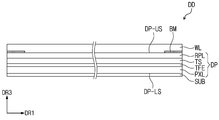
도 8a를 참조하면, 표시 패널(DP)은 베이스층(SUB), 화소층(PXL), 입력 센싱층(TS) 및 반사 방지층(RPL)을 포함할 수 있다. 다만, 이에 한정되는 것은 아니며, 표시 패널(DP)은 당 기술분야에 알려진 일반적인 구성요소를 더 포함할 수 있으며, 예를 들어, 봉지층(TFE)을 더 포함할 수 있다.8A, the display panel DP may include a base layer SUB, a pixel layer PXL, an input sensing layer TS, and an anti-reflection layer RPL. However, the present invention is not limited thereto, and the display panel DP may further include general components known in the art, for example, and may further include an encapsulation layer (TFE).
베이스층(SUB), 화소층(PXL), 입력 센싱층(TS), 반사 방지층(RPL), 봉지층(TFE)은 연속 공정을 통해 일체로 형성되는 것일 수 있으나, 이에 한정되는 것은 아니다. 입력 센싱층(TS), 반사 방지층(RPL), 봉지층(TFE) 등이 점착 부재 없이 화소층(PXL)의 상면에 배치될 수 있으며, 이 경우, 점착시 발생되는 눌림 현상 및 점착 부재의 크리프(creep) 특성에 의한 플렉서블 표시 장치의 복원성 저하 방지 효과가 더욱 우수하며, 나아가 공정을 단순화할 수 있어 플렉서블한 표시 장치를 용이하게 구현할 수 있다.The base layer SUB, the pixel layer PXL, the input sensing layer TS, the antireflection layer RPL, and the sealing layer TFE may be integrally formed through a continuous process, but the present invention is not limited thereto. The input sensing layer TS, the antireflection layer RPL and the sealing layer TFE may be disposed on the upper surface of the pixel layer PXL without an adhesive member. In this case, the effect of preventing the degradation of the stability of the flexible display device due to the creep characteristics is further improved. Further, the process can be simplified, and a flexible display device can be easily implemented.
베이스층(SUB)은 화소층(PXL), 입력 센싱층(TS), 반사 방지층(RPL), 봉지층(TFE) 등이 배치되는 기판일 수 있다. 베이스층(SUB)은 외부의 습기가 화소층(PXL)에 침투하는 것을 방지하고, 외부의 충격을 흡수할 수 있다. 베이스층(SUB)은 플렉서블한 기판일 수 있다. 베이스층(SUB)은 폴리에테르술폰(PES, polyethersulfone), 폴리아크릴레이트(PAR, polyacrylate), 폴리에테르이미드(PEI,polyetherimide), 폴리에틸렌나프탈레이트(PEN, polyethylenenapthalate), 폴리에틸렌테레프탈레이드(PET, polyethyleneterephtalate), 폴리페닐렌설파이드(PPS, polyphenylenesulfide), 폴리아릴레이트(polyarylate), 폴리이미드(PI, polyimide), 폴리카보네이트(PC, polycarbonate), 폴리아릴렌에테르술폰(poly(aryleneether sulfone)) 및 이들의 조합으로 이루어진 그룹에서 선택된 어느 하나를 포함할 수 있다.The base layer SUB may be a substrate on which the pixel layer PXL, the input sensing layer TS, the antireflection layer RPL, the sealing layer TFE, and the like are disposed. The base layer SUB prevents external moisture from penetrating into the pixel layer PXL, and can absorb an external impact. The base layer SUB may be a flexible substrate. The base layer SUB may be formed of a material selected from the group consisting of polyethersulfone (PES), polyacrylate (PAR), polyetherimide (PEI), polyethylenenaphthalate (PEN), polyethyleneterephtalate (PET) , Polyphenylenesulfide (PPS), polyarylate, polyimide (PI), polycarbonate (PC), polyarylene ether sulfone), and combinations thereof , And the like.
베이스층(SUB)을 구성하는 물질은 플라스틱 수지들에 제한되지 않고, 베이스층(SUB)은 유리 기판, 메탈 기판, 또는 유/무기 복합재료 기판 등을 포함할 수 있다.The material constituting the base layer SUB is not limited to plastic resins, and the base layer SUB may include a glass substrate, a metal substrate, or an organic / inorganic composite material substrate.
화소층(PXL)은 베이스층(SUB) 상에 배치된다. 화소층(PXL)은 입력된 영상 데이터(미도시)에 대응하여, 영상을 표시한다.The pixel layer PXL is disposed on the base layer SUB. The pixel layer PXL displays an image corresponding to input image data (not shown).
화소층(PXL)은 유기 발광 표시 패널, 전기 영동 표시 패널, 일렉트로 웨팅 표시 패널 등일 수 있고, 그 종류가 제한되지 않는다. 본 발명에서는 이하 유기 발광 표시 패널이 예시적으로 설명되고, 유기 발광 표시 패널에 대한 상세한 설명은 후술하도록 한다.The pixel layer PXL may be an organic light emitting display panel, an electrophoretic display panel, an electrowetting display panel, or the like, and the kind thereof is not limited. Hereinafter, the organic light emitting display panel will be exemplarily described in the present invention, and a detailed description of the organic light emitting display panel will be described later.
봉지층(TFE)은 화소층(PXL) 상측에 배치될 수 있다. 봉지층(TFE)은 화소층(PXL)을 밀봉하도록 배치될 수 있다. 봉지층(TFE)은 외부의 수분이나 산소에 의해서 쉽게 열화될 수 있는 화소층(PXL)을 보호하는 기능을 할 수 있다. 봉지층(TFE)은 유기 물질을 포함할 수 있고, 나아가 봉지층(TFE)은 유기층과 무기층이 적층된 구조를 가질 수 있다.The sealing layer (TFE) may be disposed on the pixel layer (PXL). The sealing layer (TFE) may be arranged to seal the pixel layer (PXL). The sealing layer (TFE) can function to protect the pixel layer (PXL) which can be easily deteriorated by external moisture or oxygen. The sealing layer (TFE) may include an organic material, and further, the sealing layer (TFE) may have a structure in which an organic layer and an inorganic layer are laminated.
입력 센싱층(TS) 및 반사 방지층(RPL)은 봉지층(TFE) 상에 배치될 수 있으며, 적층 순서는 특별히 한정되지 않는다. 예를 들어, 반사 방지층(RPL)이 봉지층(TFE)과 입력 센싱층(TS) 사이에 배치될 수도 있고, 입력 센싱층(TS)이 봉지층(TFE)과 반사 방지층(RPL) 사이에 배치될 수도 있다.The input sensing layer TS and the antireflection layer RPL may be disposed on the sealing layer TFE, and the order of lamination is not particularly limited. For example, the antireflection layer RPL may be disposed between the sealing layer TFE and the input sensing layer TS, and the input sensing layer TS may be disposed between the sealing layer TFE and the antireflection layer RPL .
입력 센싱층(TS)은 외부 입력의 좌표 정보를 획득할 수 있다. 외부 입력은 직접 터치일 수도 있고, 간접 터치일 수도 있다. 입력 센싱층(TS)은 봉지층(TFE) 상면에 배치될 수 있다. 입력 센싱층(TS)은 화소층(PXL) 및 봉지층(TFE)과 연속 공정에 의해서 형성될 수 있다. 입력 센싱층(TS)은 봉지층(TFE) 상면에 직접 배치될 수 있다. 다만, 이에 의하여 한정되는 것은 아니며, 입력 센싱층(TS)과 봉지층(TFE) 사이에 접착 부재 등이 개재될 수도 있다.The input sensing layer TS can acquire the coordinate information of the external input. External input can be direct touch or indirect touch. The input sensing layer TS may be disposed on the upper surface of the sealing layer (TFE). The input sensing layer TS may be formed by a continuous process with the pixel layer PXL and the sealing layer TFE. The input sensing layer TS may be disposed directly on the top surface of the sealing layer (TFE). However, the present invention is not limited thereto, and an adhesive member or the like may be interposed between the input sensing layer TS and the sealing layer TFE.
반사 방지층(RPL)은 입력 센싱층(TS)의 상면에 배치될 수 있다. 반사 방지층(RPL)은 표시 패널(DP)의 최외층에 배치될 수 있다.The anti-reflection layer RPL may be disposed on the upper surface of the input sensing layer TS. The antireflection layer RPL may be disposed on the outermost layer of the display panel DP.
반사 방지층(RPL)은 외부로부터 입사된 광의 반사율을 감소시킬 수 있는 층일 수 있다. 예를 들어, 반사 방지층(RPL)은 편광판과 위상 지연 필름을 포함하여 상기 입사된 광을 편광시킴으로써 반사율을 감소시키거나, 입사된 광을 상쇄 간섭시킴으로써 반사율을 감소시키거나 복수의 컬러 필터층 및 광을 흡수하는 부재(예를 들면 블랙 매트릭스)를 포함하여, 상기 입사된 광을 흡수함으로써, 반사율을 감소시킬 수 있다.The antireflection layer RPL may be a layer capable of reducing the reflectance of light incident from the outside. For example, the antireflection layer RPL may include a polarizing plate and a retardation film to reduce the reflectance by polarizing the incident light, or may reduce the reflectance by destructively interfering with the incident light, Absorbing member (for example, a black matrix), and absorbing the incident light, the reflectance can be reduced.
본 발명의 일 실시예에서, 반사 방지층(RPL)은 입력 센싱층(TS)과 연속 공정에 의해 형성될 수 있다. 본 발명의 일 실시예에서, 반사 방지층(RPL)은 입력 센싱층(TS)의 일부를 구성할 수 있다.In one embodiment of the present invention, the anti-reflection layer RPL may be formed by a continuous process with the input sensing layer TS. In one embodiment of the present invention, the antireflection layer RPL may constitute a part of the input sensing layer TS.
블랙 매트릭스(BM)는 비표시 영역(도 1의 DD-NDA)과 중첩하며, 표시 패널(DP)의 상면(DP-US)에 배치될 수 있다. 블랙 매트릭스(BM)는 광을 흡수할 수 있는 다양한 물질을 포함할 수 있다. 일반적으로 블랙 매트릭스(BM)는 블랙 안료를 혼합한 블랙 유기 물질 또는 크롬 옥사이드(CrOx) 등을 포함할 수 있다. 블랙 매트릭스(BM)는 비표시 영역(도 1의 DD-NDA)과 중첩되도록 배치됨으로써, 표시 장치(DD)를 구동하기 위해 사용하는 배선들이 외부에서 시인되지 않도록 하고, 외광을 흡수함으로써 외광 반사를 줄이는 기능을 할 수 있다. 예를 들어, 블랙 매트릭스(BM)는 평면상에서 비표시 영역(도 1의 DD-NDA) 전체와 중첩할 수 있다.The black matrix BM overlaps with the non-display area (DD-NDA in FIG. 1) and can be disposed on the upper surface DP-US of the display panel DP. The black matrix (BM) may include various materials capable of absorbing light. In general, the black matrix (BM) may include a black organic material mixed with a black pigment or chromium oxide (CrOx) or the like. The black matrix BM is arranged so as to overlap the non-display area (DD-NDA in FIG. 1), thereby preventing wirings used for driving the display device DD from being visually recognized from the outside and absorbing external light, Can be reduced. For example, the black matrix BM may overlap the entire non-display area (DD-NDA in FIG. 1) on a plane.
윈도우 코팅층(WL)은 도 8a에서 반사 방지층(RPL)의 외면 및 블랙 매트릭스(BM)의 외면, 즉 반사 방지층(RPL)의 상면 및 블랙 매트릭스(BM)의 상면에 직접 배치될 수 있다. 이 경우, 표시 패널(DP)의 상면(DP-US)은 반사 방지층(RPL)의 상면 및 블랙 매트릭스(BM)의 상면이 될 수 있다. 윈도우 코팅층(WL)은 전술한 바와 같이 OCA(optical clear adhesive), OCR(optical clear resin), PSA(pressure sensitive adhesive)와 같은 접착 부재들 없이 반사 방지층(RPL)의 상면 및 블랙 매트릭스(BM)의 상면에 직접 배치될 수 있다. The window coating layer WL may be disposed directly on the outer surface of the antireflection layer RPL and on the outer surface of the black matrix BM, that is, on the upper surface of the antireflection layer RPL and the upper surface of the black matrix BM in Fig. In this case, the upper surface DP-US of the display panel DP can be the upper surface of the antireflection layer RPL and the upper surface of the black matrix BM. The window coating layer WL is formed on the upper surface of the antireflection layer RPL and the upper surface of the black matrix BM without adhesion members such as optical clear adhesive (OCA), optical clear resin (OCR), pressure sensitive adhesive (PSA) Can be disposed directly on the upper surface.
도 8b 내지 도 8d에 도시된 바와 같이 표시 패널(DP)이 포함하는 층들의 적층 구조는 다양하게 변경될 수 있다.As shown in FIGS. 8B to 8D, the lamination structure of the layers included in the display panel DP can be variously changed.
도 8b를 참조하면, 표시 패널(DP)의 반사 방지층(RPL)은 봉지층(TFE) 상면에 배치될 수 있고, 입력 센싱층(TS)은 반사 방지층(RPL) 상면에 배치될 수 있다. 즉, 입력 센싱층(TS)은 표시 패널(DP)에서 최외층일 수 있고, 이 경우 표시 패널(DP)의 상면(DP-US)은 입력 센싱층(TS)의 외면 즉 입력 센싱층(TS)의 상면일 수 있으며, 윈도우 코팅층(WL)은 입력 센싱층(TS)의 상면에 직접 배치될 수 있다.8B, the antireflection layer RPL of the display panel DP may be disposed on the top surface of the sealing layer TFE, and the input sensing layer TS may be disposed on the top surface of the antireflection layer RPL. That is, the input sensing layer TS may be the outermost layer in the display panel DP. In this case, the top surface DP-US of the display panel DP is an outer surface of the input sensing layer TS, And the window coating layer WL may be disposed directly on the upper surface of the input sensing layer TS.
도 8c를 참조하면, 반사 방지층(RPL, 도 2a에 도시됨)은 입력 센싱층(TS-R)에 통합될 수 있다. 즉, 반사 방지층(RPL)은 입력 센싱층(TS-R)의 일부를 구성할 수 있다. 즉, 입력 센싱층(TS-R)은 표시 패널(DP)의 최외층일 수 있고, 이 경우 표시 패널(DP)의 상면(DP-US)은 입력 센싱층(TS-R)의 외면, 즉 입력 센싱층(TS-R)의 상면일 수 있으며, 윈도우 코팅층(WL)은 입력 센싱층(TS-R)의 상면에 직접 배치될 수 있다.Referring to FIG. 8C, an antireflection layer (RPL, shown in FIG. 2A) may be incorporated into the input sensing layer TS-R. That is, the antireflection layer RPL may constitute a part of the input sensing layer TS-R. That is, the input sensing layer TS-R may be the outermost layer of the display panel DP. In this case, the top surface DP-US of the display panel DP is the outer surface of the input sensing layer TS- May be the upper surface of the input sensing layer TS-R, and the window coating layer WL may be disposed directly on the upper surface of the input sensing layer TS-R.
도 8d를 참조하면, 반사 방지층(RPL, 도 2a에 도시됨)이 화소층(PXL-R)에 통합될 수 있다. 즉, 반사 방지층(RPL)은 화소층(PXL-R)의 일부를 구성할 수 있다. 즉, 입력 센싱층(TS)은 표시 패널(DP)의 최외층일 수 있고, 이 경우 표시 패널(DP)의 상면(DP-US)은 입력 센싱층(TS)의 외면, 즉 입력 센싱층(TS)의 상면일 수 있고, 윈도우 코팅층(WL)은 입력 센싱층(TS)의 상면에 직접 배치될 수 있다.Referring to FIG. 8D, an antireflection layer (RPL, shown in FIG. 2A) may be incorporated into the pixel layer PXL-R. That is, the antireflection layer RPL may constitute a part of the pixel layer PXL-R. That is, the input sensing layer TS may be the outermost layer of the display panel DP. In this case, the top surface DP-US of the display panel DP is an outer surface of the input sensing layer TS, TS), and the window coating layer WL may be disposed directly on the upper surface of the input sensing layer TS.
이상 표시 패널(DP)이 포함하는 층들의 다양한 적층구조 예시적으로 설명하였으나, 이에 한정되지 않으며 표시 패널(DP)이 포함하는 층들은 다양한 순서로 적층될 수 있다. Although various laminated structures of the layers including the ideal display panel DP have been described by way of example, the present invention is not limited thereto, and the layers including the display panel DP may be stacked in various orders.
도 9는 본 발명의 일 실시예에 따른 표시 장치의 사시도이다. 도 10은 본 발명의 일 실시예에 따른 표시 장치에 포함되는 화소들 중 하나의 회로도이다. 도 11은 도 10에 따른 회로도 일부의 개략적인 단면도이다.9 is a perspective view of a display device according to an embodiment of the present invention. 10 is a circuit diagram of one of the pixels included in the display device according to the embodiment of the present invention. 11 is a schematic cross-sectional view of a portion of the circuit diagram according to Fig.
이하, 도 9 내지 도 11을 참조하여, 본 발명의 일 실시예에 따른 표시 장치가 유기 전계 발광 표시 장치인 것을 예시적으로 설명한다. 다시 말해, 이하에서는 화소층(PXL)이 유기 전계 발광 소자(OEL)를 포함하는 것을 예를 들어 설명한다. 다만, 이에 한정되는 것은 아니다.Hereinafter, with reference to FIGS. 9 to 11, a display device according to an exemplary embodiment of the present invention will be described as an organic light emitting display device. In other words, the pixel layer PXL includes an organic electroluminescent device OEL, for example, in the following description. However, the present invention is not limited thereto.
도 9를 참조하면, 전술한 바와 같이, 본 발명의 일 실시예에 따른 표시 장치(DD)는 표시 영역(DD-DA) 및 비표시 영역(DD-NDA)으로 구분된다. 표시 영역(DD-DA)은 복수의 화소 영역들(PA)을 포함한다. 화소 영역들(PA)은 매트릭스 형태로 배치될 수 있다. 화소 영역들(PA)에는 복수의 화소들(PX)이 배치될 수 있다. 화소들(PX) 각각은 유기 전계 발광 소자(예를 들어, 도 10의 OEL)를 포함할 수 있다.Referring to FIG. 9, the display device DD according to an embodiment of the present invention is divided into a display area DD-DA and a non-display area DD-NDA, as described above. The display area DD-DA includes a plurality of pixel areas PA. The pixel regions PA may be arranged in a matrix form. A plurality of pixels PX may be arranged in the pixel regions PA. Each of the pixels PX may include an organic electroluminescent device (e.g., the OEL in FIG. 10).
도 10을 참조하면, 화소들(PX) 각각은 게이트 라인(GL), 데이터 라인(DL) 및 구동 전압 라인(DVL)으로 이루어진 배선부와 연결될 수 있다. 화소들(PX) 각각은 배선부에 연결된 박막 트랜지스터(TFT1, TFT2), 박막 트랜지스터(TFT1, TFT2)에 연결된 유기 전계 발광 소자(OEL) 및 커패시터(Cst)를 포함한다.Referring to FIG. 10, each of the pixels PX may be connected to a wiring portion composed of a gate line GL, a data line DL, and a driving voltage line DVL. Each of the pixels PX includes thin film transistors TFT1 and TFT2 connected to a wiring portion, an organic electroluminescence element OEL connected to the thin film transistors TFT1 and TFT2 and a capacitor Cst.
게이트 라인(GL)은 제1 방향(DR1)으로 연장된다. 데이터 라인(DL)은 게이트 라인(GL)과 교차하는 제2 방향(DR2)으로 연장된다. 구동 전압 라인(DVL)은 데이터 라인(DL)과 실질적으로 동일한 방향, 즉 제2 방향(DR2)으로 연장된다. 게이트 라인(GL)은 박막 트랜지스터(TFT1, TFT2)에 주사 신호를 전달하고, 데이터 라인(DL)은 박막 트랜지스터(TFT1, TFT2)에 데이터 신호를 전달하며, 구동 전압 라인(DVL)은 박막 트랜지스터(TFT1, TFT2)에 구동 전압을 제공한다.The gate line GL extends in the first direction DR1. The data line DL extends in the second direction DR2 intersecting the gate line GL. The driving voltage line DVL extends substantially in the same direction as the data line DL, i.e., in the second direction DR2. The gate line GL transmits a scan signal to the thin film transistors TFT1 and TFT2 and the data line DL transmits a data signal to the thin film transistors TFT1 and TFT2 while the drive voltage line DVL is a thin film transistor TFT1 and TFT2.
박막 트랜지스터(TFT1, TFT2)는 유기 전계 발광 소자(OEL)를 제어하기 위한 구동 박막 트랜지스터(TFT1)와, 구동 박막 트랜지스터(TFT1)를 스위칭 하는 스위칭 박막 트랜지스터(TFT2)를 포함할 수 있다. 본 발명이 일 실시예에서는 화소들(PX) 각각이 두 개의 박막 트랜지스터(TFT1, TFT2)를 포함하는 것을 설명하나, 이에 한정되는 것은 아니고, 화소들(PX) 각각이 하나의 박막 트랜지스터와 커패시터를 포함할 수도 있고, 화소들(PX) 각각이 셋 이상의 박막 트랜지스터와 둘 이상의 커패시터를 구비할 수도 있다.The thin film transistors TFT1 and TFT2 may include a driving thin film transistor TFT1 for controlling the organic electroluminescence element OEL and a switching thin film transistor TFT2 for switching the driving thin film transistor TFT1. The present invention is not limited to this, and each pixel PX may include a single thin film transistor and a capacitor (not shown). In the present embodiment, each of the pixels PX includes two thin film transistors TFT1 and TFT2, Or each of the pixels PX may include three or more thin film transistors and two or more capacitors.
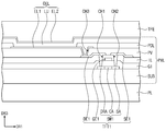
도 11을 구체적으로, 도 10의 구동 박막 트랜지스터(TFT1) 및 유기 전계 발광 소자(OEL)에 해당하는 부분의 개략적인 단면도이다.11 is a schematic cross-sectional view of a portion corresponding to the driving thin film transistor TFT1 and the organic electroluminescence element OEL in Fig. 10 in detail.
도 10 및 도 11을 참조하면, 구동 박막 트랜지스터(TFT1)는 제1 게이트 전극(GE1), 제1 소스 전극(SE1) 및 제1 드레인 전극(DE1)을 포함한다. 제1 게이트 전극(GE1)은 제1 공통 전극(미도시)에 연결된다. 제1 소스 전극(SE1)은 구동 전압 라인(DVL)에 연결된다. 제1 드레인 전극(DE1)은 제3 콘택홀(CH3)에 의해 제1 전극(EL1)과 연결된다.10 and 11, the driving thin film transistor TFT1 includes a first gate electrode GE1, a first source electrode SE1, and a first drain electrode DE1. The first gate electrode GE1 is connected to a first common electrode (not shown). The first source electrode SE1 is connected to the driving voltage line DVL. The first drain electrode DE1 is connected to the first electrode EL1 by the third contact hole CH3.
커패시터(Cst)는 구동 박막 트랜지스터(TFT1)의 제1 게이트 전극(GE1)과 제1 소스 전극(SE1) 사이에 연결되며, 구동 박막 트랜지스터(TFT1)의 제1 게이트 전극(GE1)에 입력되는 데이터 신호를 충전하고 유지한다.The capacitor Cst is connected between the first gate electrode GE1 and the first source electrode SE1 of the driving thin film transistor TFT1 and connected to the data input to the first gate electrode GE1 of the driving thin film transistor TFT1 Charge and hold the signal.
구동 박막 트랜지스터(TFT1)와 유기 전계 발광 소자(OEL)는 베이스층(SUB) 상에 배치된다. 베이스층(SUB) 상에는 기판 버퍼층(미도시)이 배치될 수 있다. 기판 버퍼층 (미도시)은 구동 박막 트랜지스터(TFT1) 및 스위칭 박막 트랜지스터(TFT2)에 불순물이 확산되는 것을 막는다. 기판 버퍼층(미도시)은 질화규소(SiNx), 산화규소(SiOx), 질산화규소(SiOxNy) 등으로 형성될 수 있으며, 베이스층(SUB)의 재료 및 공정 조건에 따라 생략될 수도 있다.The driving thin film transistor TFT1 and the organic electroluminescence element OEL are disposed on the base layer SUB. A substrate buffer layer (not shown) may be disposed on the base layer SUB. The substrate buffer layer (not shown) prevents impurities from diffusing into the driving thin film transistor TFT1 and the switching thin film transistor TFT2. The substrate buffer layer (not shown) may be formed of silicon nitride (SiNx), silicon oxide (SiOx), silicon oxynitride (SiOxNy) or the like and may be omitted depending on the material and process conditions of the base layer SUB.
베이스층(SUB) 상에는 제1 반도체층(SM1)이 배치된다. 구체적으로 도시하지는 않았으나, 제1 반도체층(SM1)은 반도체 소재로 형성되며, 구동 박막 트랜지스터(TFT1)의 활성층으로 동작한다. 제1 반도체층(SM1)은 소스 영역(SA), 드레인 영역(DRA) 및 소스 영역(SA)과 드레인 영역(DRA) 사이에 배치된 채널 영역(CA)을 포함한다. 제1 반도체층(SM1)은 무기 반도체 또는 유기 반도체로부터 선택되어 형성될 수 있다. 소스 영역(SA) 및 드레인 영역(DRA)은 n형 불순물 또는 p형 불순물이 도핑될 수 있다.The first semiconductor layer SM1 is disposed on the base layer SUB. Although not specifically shown, the first semiconductor layer SM1 is formed of a semiconductor material and operates as an active layer of the driving thin film transistor TFT1. The first semiconductor layer SM1 includes a source region SA, a drain region DRA and a channel region CA disposed between the source region SA and the drain region DRA. The first semiconductor layer SM1 may be formed of an inorganic semiconductor or an organic semiconductor. The source region SA and the drain region DRA may be doped with an n-type impurity or a p-type impurity.
제1 반도체층(SM1) 상에는 게이트 절연층(GI)이 배치된다. 게이트 절연층(GI)은 제1 반도체층(SM1)을 커버한다. 게이트 절연층(GI)은 유기 절연물 또는 무기 절연물로 이루어질 수 있다.A gate insulating layer GI is disposed on the first semiconductor layer SM1. The gate insulating layer GI covers the first semiconductor layer SM1. The gate insulating layer (GI) may be formed of an organic insulating material or an inorganic insulating material.
게이트 절연층(GI) 상에는 제1 게이트 전극(GE1)이 배치된다. 제1 게이트 전극(GE1)은 제1 반도체층(SM1)의 채널 영역(CA)에 대응되는 영역을 커버하도록 형성된다.A first gate electrode GE1 is disposed on the gate insulating layer GI. The first gate electrode GE1 is formed to cover a region corresponding to the channel region CA of the first semiconductor layer SM1.
제2 게이트 전극(GE2) 상에는 층간 절연층(IL)이 배치된다. 층간 절연층(IL)은 제1 게이트 전극(GE1)을 커버한다. 층간 절연층(IL)은 유기 절연물 또는 무기 절연물로 이루어질 수 있다.An interlayer insulating layer IL is disposed on the second gate electrode GE2. The interlayer insulating layer IL covers the first gate electrode GE1. The interlayer insulating layer IL may be formed of an organic insulating material or an inorganic insulating material.
층간 절연층(IL)의 상에는 제1 소스 전극(SE1)과 제1 드레인 전극(DE1)이 배치된다. 제1 드레인 전극(DE1)은 게이트 절연층(GI) 및 층간 절연층(IL)에 형성된 제1 콘택홀(CH1)에 의해 제1 반도체층(SM1)의 드레인 영역(DRA)과 접촉하고, 제1 소스 전극(SE1)은 게이트 절연층(GI) 및 층간 절연층(IL)에 형성된 제2 콘택홀(CH2)에 의해 제1 반도체층(SM1)의 소스 영역(SA)과 접촉한다. A first source electrode SE1 and a first drain electrode DE1 are disposed on the interlayer insulating layer IL. The first drain electrode DE1 is in contact with the drain region DRA of the first semiconductor layer SM1 by the first contact hole CH1 formed in the gate insulating layer GI and the interlayer insulating layer IL, 1 source electrode SE1 is in contact with the source region SA of the first semiconductor layer SM1 by the gate insulating layer GI and the second contact hole CH2 formed in the interlayer insulating layer IL.
제1 소스 전극(SE1) 및 제1 드레인 전극(DE1) 상에는 패시베이션층(PV)이 배치된다. 패시베이션층(PV)은 구동 박막 트랜지스터(TFT1)를 보호하는 보호막의 역할을 할 수도 있고, 그 상면을 평탄화시키는 평탄화층의 역할을 할 수도 있다.A passivation layer PV is disposed on the first source electrode SE1 and the first drain electrode DE1. The passivation layer PV may serve as a protective film for protecting the driving thin film transistor TFT1 and may serve as a planarization layer for planarizing the upper surface thereof.
패시베이션층(PV) 상에는 유기 전계 발광 소자(OEL)가 배치된다. 유기 전계 발광 소자(OEL)는 제1 전극(EL1), 제1 전극(EL1) 상에 배치된 제2 전극(EL2), 및 제1 전극(EL1) 및 제2 전극(EL2) 사이에 배치된 발광 유닛(LU)을 포함한다.An organic electroluminescent device (OEL) is disposed on the passivation layer (PV). The organic electroluminescent device OEL includes a first electrode EL1, a second electrode EL2 disposed on the first electrode EL1, and a second electrode EL2 disposed between the first electrode EL1 and the second electrode EL2 And a light emitting unit (LU).
구체적으로, 패시베이션층(PV) 상에는 제1 전극(EL1)이 배치되고, 패시베이션층(PV) 및 제1 전극(EL1) 상에는 화소 정의막(PDL)이 배치된다. 화소 정의막(PDL)은 제1 전극(EL1)의 상면의 일부를 노출시킨다. 화소 정의막(PDL)은 이에 한정하는 것은 아니나, 금속-불소 이온 화합물을 포함할 수 있다. Specifically, the first electrode EL1 is disposed on the passivation layer PV, and the pixel defining layer PDL is disposed on the passivation layer PV and the first electrode EL1. The pixel defining layer PDL exposes a part of the upper surface of the first electrode EL1. The pixel defining layer (PDL) may include, but is not limited to, a metal-fluorine ion compound.
화소 정의막(PDL) 및 제1 전극(EL1) 상에 발광 유닛(LU) 및 제2 전극(EL2)이 순차적으로 배치된다. 제1 전극(EL1)은 예를 들어 양극일 수 있다. 제1 전극(EL1)은 패시베이션층(PV)에 형성되는 제3 콘택홀(CH3)을 통해 구동 박막 트랜지스터(TFT1)의 제1 드레인 전극(DE1)에 연결된다.The light emitting unit LU and the second electrode EL2 are sequentially arranged on the pixel defining layer PDL and the first electrode EL1. The first electrode EL1 may be, for example, a cathode. The first electrode EL1 is connected to the first drain electrode DE1 of the driving thin film transistor TFT1 through the third contact hole CH3 formed in the passivation layer PV.
제1 전극(EL1)은 도전성을 갖는다. 제1 전극(EL1)은 화소 전극 또는 양극일 수 있다. 제1 전극(EL1)은 투과형 전극, 반투과형 전극 또는 반사형 전극일 수 있다. 제1 전극(EL1)이 투과형 전극인 경우, 제1 전극(EL1)은 투명 금속 산화물, 예를 들어, ITO(indium tin oxide), IZO(indium zinc oxide), ZnO(zinc oxide) 또는 ITZO(indium tin zinc oxide)를 포함할 수 있다. 제1 전극(EL1)이 반투과형 전극 또는 반사형 전극인 경우, 제1 전극(EL1)은 Ag, Mg, Al, Pt, Pd, Au, Ni, Nd, Ir, Cr 또는 금속의 혼합물을 포함할 수 있다.The first electrode EL1 has conductivity. The first electrode EL1 may be a pixel electrode or an anode. The first electrode EL1 may be a transmissive electrode, a transflective electrode, or a reflective electrode. When the first electrode EL1 is a transmissive electrode, the first electrode EL1 may be formed of a transparent metal oxide such as ITO (indium tin oxide), IZO (indium zinc oxide), ZnO (zinc oxide), ITZO tin zinc oxide). When the first electrode EL1 is a transflective electrode or a reflective electrode, the first electrode EL1 includes a mixture of Ag, Mg, Al, Pt, Pd, Au, Ni, Nd, .
제2 전극(EL2)은 공통 전극 또는 음극일 수 있다. 제2 전극(EL2)은 투과형 전극, 반투과형 전극 또는 반사형 전극일 수 있다.The second electrode EL2 may be a common electrode or a cathode. The second electrode EL2 may be a transmissive electrode, a transflective electrode, or a reflective electrode.
제2 전극(EL2)이 투과형 전극인 경우, 제2 전극(EL2)은 Li, Ca, LiF/Ca, LiF/Al, Al, Mg, BaF, Ba, Ag 또는 이들의 화합물이나 혼합물(예를 들어, Ag와 Mg의 혼합물)을 포함할 수 있다. 다만, 이에 의하여 한정되는 것은 아니며, 예를 들어, ITO(indium tin oxide), IZO(indium zinc oxide), ZnO(zinc oxide) 또는 ITZO(indium tin zinc oxide)를 포함하는 것일 수도 있다.In the case where the second electrode EL2 is a transmissive electrode, the second electrode EL2 may be formed of any of Li, Ca, LiF / Ca, LiF / Al, Al, Mg, BaF, Ba, Ag, , A mixture of Ag and Mg). However, the present invention is not limited thereto, and may include, for example, ITO (indium tin oxide), IZO (indium zinc oxide), ZnO (zinc oxide), or ITZO (indium tin zinc oxide).
도시하지는 않았으나, 제2 전극(EL2)은 보조 전극과 연결될 수 있다. 보조 전극은 당 기술분야에 알려진 재료라면 제한없이 채용될 수 있다. 예를 들어, 보조 전극은 Li, Ca, LiF/Ca, LiF/Al, Al, Mg, BaF, Ba, Ag 또는 이들의 화합물이나 혼합물(예를 들어, Ag와 Mg의 혼합물)을 포함하는 것일 수 있다. 다만, 이에 의하여 한정되는 것은 아니고, 보조 전극은 ITO(indium tin oxide), IZO(indium zinc oxide), ZnO(zinc oxide) 또는 ITZO(indium tin zinc oxide)를 포함할 수도 있다. 예를 들어, 보조 전극은 제2 전극(EL2)과 연결되어, 제2 전극(EL2)의 저항값을 낮추는 역할을 수행할 수 있다.Although not shown, the second electrode EL2 may be connected to the auxiliary electrode. The auxiliary electrode can be employed without limitation as long as it is a material known in the art. For example, the auxiliary electrode may comprise Li, Ca, LiF / Ca, LiF / Al, Al, Mg, BaF, Ba, Ag or a compound or mixture thereof (e.g. a mixture of Ag and Mg) have. However, the present invention is not limited thereto, and the auxiliary electrode may include ITO (indium tin oxide), IZO (indium zinc oxide), ZnO (zinc oxide), or ITZO (indium tin zinc oxide). For example, the auxiliary electrode may be connected to the second electrode EL2 to lower the resistance value of the second electrode EL2.
제2 전극(EL2)이 반투과형 전극 또는 반사형 전극인 경우, 제2 전극(EL2)은 Ag, Mg, Al, Pt, Pd, Au, Ni, Nd, Ir, Cr, Li, Ca, LiF/Ca, LiF/Al, Mo, Ti 또는 이들의 화합물이나 혼합물(예를 들어, Ag와 Mg의 혼합물)을 포함할 수 있다. 또는 상기 물질로 형성된 반사막이나 반투과막 및 ITO(indium tin oxide), IZO(indium zinc oxide), ZnO(zinc oxide), ITZO(indium tin zinc oxide) 등으로 형성된 투명 도전막을 포함하는 복수의 층 구조일 수 있다.The second electrode EL2 may be formed of Ag, Mg, Al, Pt, Pd, Au, Ni, Nd, Ir, Cr, Li, Ca, LiF / Ca, LiF / Al, Mo, Ti, or a compound or mixture thereof (for example, a mixture of Ag and Mg). Or a transparent conductive film formed of a reflective film or a semi-transmissive film formed of the above material and indium tin oxide (ITO), indium zinc oxide (IZO), zinc oxide (ZnO), indium tin zinc oxide Lt; / RTI >
제1 전극(EL1) 및 제2 전극(EL2) 사이에 배치된 발광 유닛(LU)은 유기층일 수 있다. 발광 유닛(LU)은 제1 전극(EL1) 상에 배치된 정공 수송 영역, 정공 수송 영역 상에 배치된 발광층, 및 발광층 상에 전자 수송 영역을 포함할 수 있다. 정공 수송 영역, 발광층, 및 전자 수송 영역은 당 기술분야에 알려진 일반적인 것을 제한없이 채용할 수 있다.The light emitting unit LU disposed between the first electrode EL1 and the second electrode EL2 may be an organic layer. The light emitting unit LU may include a hole transporting region disposed on the first electrode EL1, a light emitting layer disposed on the hole transporting region, and an electron transporting region on the light emitting layer. The hole transporting region, the light emitting layer, and the electron transporting region may be employed without limitation as those generally known in the art.
정공 수송 영역은 복수의 서로 다른 물질로 이루어진 단일층의 구조를 갖거나, 제1 전극(EL1)으로부터 차례로 적층된 정공 주입층/정공 수송층, 정공 주입층/정공 수송층/정공 버퍼층, 정공 주입층/정공 버퍼층, 정공 수송층/정공 버퍼층 또는 정공 주입층/정공 수송층/전자 저지층의 구조를 가질 수 있으나, 이에 한정되는 것은 아니다.The hole transporting region may have a structure of a single layer made of a plurality of different materials, or may have a structure of a single layer composed of a plurality of different materials, a hole injection layer / hole transport layer, a hole injection layer / hole transport layer / hole buffer layer, A hole transport layer / hole buffer layer, a hole injection layer / a hole transport layer / an electron blocking layer, but the present invention is not limited thereto.
발광층은 단일 물질로 이루어진 단일층, 복수의 서로 다른 물질로 이루어진 단일층 또는 복수의 서로 다른 물질로 이루어진 복수의 층을 갖는 다층 구조를 가질 수 있다. 발광층은 호스트 및 도펀트를 포함할 수 있다.The light emitting layer may have a single layer made of a single material, a single layer made of a plurality of different materials, or a multi-layered structure having a plurality of layers made of a plurality of different materials. The light emitting layer may include a host and a dopant.
전자 수송 영역은 정공 저지층, 전자 수송층 및 전자 주입층 중 적어도 하나를 포함할 수 있으나, 이에 한정되는 것은 아니다.The electron transporting region may include at least one of a hole blocking layer, an electron transporting layer and an electron injection layer, but is not limited thereto.
전술한 봉지층(TFE)은 제2 전극(EL2) 상에 배치될 수 있으며, 예를 들어, 제2 전극(EL2)의 상면에 직접 배치될 수 있다.The above-mentioned sealing layer (TFE) may be disposed on the second electrode EL2, for example, and may be disposed directly on the upper surface of the second electrode EL2.
도 12는 본 발명의 일 실시예에 따른 표시 장치의 개략적인 단면도이다. 12 is a schematic cross-sectional view of a display device according to an embodiment of the present invention.
도 1 및 도 12를 참조하면, 본 발명의 일 실시예에 따른 표시 장치(DD)는 제1 컬 방지 패턴(CP1)을 더 포함하는 것일 수 있다. 제1 컬 방지 패턴(CP1)은 표시 패널(DP)의 상면(DP-US)에 배치될 수 있다. 제1 컬 방지 패턴(CP1)은 윈도우 코팅층(WL)에 의해 커버될 수 있다. 표시 장치(DD)는 제1 컬 방지 패턴(CP1)을 포함함으로써, 윈도우 코팅층(WL)을 형성하는 과정에서 윈도우 코팅층(WL)의 경화 수축 및 윈도우 코팅층(WL) 내부에서의 열팽창 계수 차이에 의해서 발생될 수 있는 들뜸 현상 또는 컬(curl) 현상을 방지할 수 있다.Referring to FIGS. 1 and 12, the display device DD according to an embodiment of the present invention may further include a first curl prevention pattern CP1. The first curl preventing pattern CP1 may be disposed on the upper surface DP-US of the display panel DP. The first curl preventing pattern CP1 may be covered by the window coating layer WL. The display device DD includes the first curl preventing pattern CP1 so that the curl shrinkage of the window coating layer WL and the thermal expansion coefficient difference in the window coating layer WL during the formation of the window coating layer WL It is possible to prevent a floating phenomenon or a curl phenomenon that may occur.
표시 영역(DD-DA)은 발광 영역 및 비발광 영역으로 구분될 수 있고, 제1 컬 방지 패턴(CP1)은 비발광 영역에 중첩하게 배치되는 것이 바람직하다. 제1 컬 방지 패턴(CP1)은 증착, 스크린 프린팅 등의 방법에 의해서 형성될 수 있다. 제1 컬 방지 패턴(CP1)의 탄성 계수는 윈도우 코팅층(WL)의 제3 영역(도 4의 AR3)의 탄성 계수보다 큰 것일 수 있다. The display area DD-DA may be divided into a light emitting area and a non-light emitting area, and the first curl preventing pattern CP1 is preferably arranged to overlap the non-light emitting area. The first curl preventing pattern CP1 may be formed by a method such as vapor deposition, screen printing or the like. The elastic modulus of the first curl preventing pattern CP1 may be larger than the elastic modulus of the third region (AR3 in FIG. 4) of the window coating layer WL.
도시하지는 않았으나, 본 발명의 일 실시예에 따른 표시 장치(DD)가 표시 패널(DP) 하면(DP-LS)에 직접 배치되는 베이스 코팅층(도 7, PL)을 포함하는 경우, 본 발명의 일 실시에에 따른 표시 장치(DD)는 표시 패널(DP)의 하면(DP-LS)에 배치되는 제2 컬 방지 패턴을 더 포함할 수 있다. 제2 컬 방지 패턴은 베이스 코팅층(도 7, PL)에 의해 커버될 수 있다.Although not shown, when the display device DD according to an embodiment of the present invention includes a base coating layer (PL, FIG. 7) directly disposed on the display panel DP and on the lower surface DP-LS, The display device DD according to the embodiment may further include a second curl preventing pattern disposed on the lower surface DP-LS of the display panel DP. The second curl preventing pattern can be covered by the base coating layer (Fig. 7, PL).
본 발명의 일 실시예에 따른 표시 장치(DD)는 필요에 따라 추가 구성요소를 더 포함할 수 있다. 도시하지는 않았으나, 예를 들어, 표시 패널(DP)은 윈도우 코팅층(WL) 배치 시, 불순물 침투, 코팅성 저하, 공정 데미지(damage) 등을 방지하기 위해 최상층으로 질화규소(SiNx), 산화규소(SiOx), 질산화규소(SiOxNy), 리튬플루오라이드(LiF) 등의 무기물 또는 유기물을 포함하는 배리어층을 포함할 수 있다. 이 경우, 배리어층의 상면이 표시 패널(DP)의 상면(DP-US)이 될 수 있다.The display device DD according to an embodiment of the present invention may further include additional components as needed. For example, the display panel DP may include silicon nitride (SiNx), silicon oxide (SiOx), and silicon oxide (SiOx) to prevent impurities penetration, coating deterioration, ), Silicon oxynitride (SiO x N y), lithium fluoride (LiF), or the like. In this case, the upper surface of the barrier layer can be the upper surface (DP-US) of the display panel DP.
본 발명의 일 실시예에 따른 표시 장치는 상부로 갈수록 탄성 계수가 커지는 영역을 포함하는 윈도우 코팅층을 표시 패널의 상면에 직접 배치한다. 점착 부재 없이 표시 패널의 상면에 바로 배치되는 종래의 윈도우 코팅층의 경우, 탄성 계수가 비교적 낮아 벤딩 시에는 유리하나 내구성이 약하다는 문제가 있다. 이러한 문제를 해결하기 위해, 윈도우 코팅층 상면에 하드 코팅층을 배치하는 구조가 제안되었으나, 윈도우 코팅층과 하드 코팅층 사이의 급격한 물성 차이(예를 들어, 탄성 계수 차이)로 인해 표면 변형 또는 박리 현상 등이 발생한다는 문제가 있다. 본 발명의 일 실시예에 따른 표시 장치는 표시 패널과 인접한 영역은 탄성 계수가 비교적 낮고, 표시 패널과 먼 영역은 탄성 계수가 비교적 높은 탄성 계수 구배를 갖는 윈도우 코팅층을 배치시켜, 우수한 가요성 및 내구성을 동시에 확보할 수 있다. 또한, 윈도우 코팅층이 탄성 계수가 상이한 복수 개의 층을 적층한 구조를 포함하는 것이 아니라 탄성 계수가 점차적으로 변하는 단일층 구조를 포함함으로써 급격한 탄성 계수 차이에 의한 층간 박리 현상 등의 문제점도 해결할 수 있다.The display device according to an embodiment of the present invention directly disposes a window coating layer including an area having a larger elastic modulus on the upper surface of the display panel. In the case of the conventional window coating layer disposed directly on the upper surface of the display panel without the adhesive member, the elastic modulus is relatively low, which is advantageous when bending, but is poor in durability. In order to solve such a problem, a structure in which a hard coating layer is disposed on the upper surface of the window coating layer has been proposed. However, due to a sudden physical property difference between the window coating layer and the hard coating layer (for example, . The display device according to an embodiment of the present invention is characterized in that a window coating layer having a relatively low modulus of elasticity in a region adjacent to the display panel and a modulus of elasticity modulus having a relatively high modulus of elasticity in a region far from the display panel is disposed, Can be secured at the same time. Further, the window coating layer does not include a structure in which a plurality of layers having different elastic moduli are stacked, but also includes a single layer structure in which the modulus of elasticity gradually changes, thereby solving problems such as delamination due to a difference in elastic modulus.
이상, 첨부된 도면을 참조하여 본 발명의 실시예를 설명하였지만, 본 발명이 속하는 기술분야에서 통상의 지식을 가진 자는 본 발명이 그 기술적 사상이나 필수적인 특징으로 변경하지 않고서 다른 구체적인 형태로 실시될 수 있다는 것을 이해할 수 있을 것이다. 그러므로 이상에서 기술한 실시예는 모든 면에서 예시적인 것이며 한정적이 아닌 것으로 이해해야만 한다.While the present invention has been described in connection with what is presently considered to be practical exemplary embodiments, it is to be understood that the invention is not limited to the disclosed embodiments, but, on the contrary, It will be understood. It is therefore to be understood that the above-described embodiments are illustrative and non-restrictive in every respect.
WL: 윈도우 코팅층
DP: 표시 패널
DP-US: 표시 패널의 상면
DP-LS: 표시 패널의 하면WL: Window coating layer DP: Display panel
DP-US: Top surface of the display panel DP-LS:
Claims (20)
상기 표시 패널의 상면에 직접 배치되는 윈도우 코팅층을 포함하고,
상기 윈도우 코팅층은
상기 표시 패널에서 상기 윈도우 코팅층 방향으로 갈수록 탄성 계수가 증가하는 제1 영역을 포함하는 것인 표시 장치.Display panel; And
And a window coating layer disposed directly on an upper surface of the display panel,
The window coating layer
And a first region where the elastic modulus increases from the display panel toward the window coating layer.
상기 윈도우 코팅층은
2종 이상의 베이스 수지(resin)를 포함하는 것인 표시 장치.The method according to claim 1,
The window coating layer
And at least two kinds of base resins.
상기 윈도우 코팅층은
상기 제1 영역을 사이에 두고 서로 이격된 제2 영역 및 제3 영역을 포함하고,
상기 제2 영역 및 상기 제3 영역은 각각 일정한 탄성 계수를 갖는 표시 장치.The method according to claim 1,
The window coating layer
A second region and a third region that are spaced apart from each other with the first region interposed therebetween,
Wherein the second region and the third region each have a constant elastic modulus.
상기 제2 영역은 상기 윈도우 코팅층의 상면을 포함하고,
상기 제3 영역은 상기 표시 패널의 상기 상면과 접촉하는 상기 윈도우 코팅층의 하면을 포함하며,
상기 제2 영역의 탄성 계수는 상기 제3 영역의 탄성 계수보다 큰 것인 표시 장치.The method of claim 3,
Wherein the second region comprises an upper surface of the window coating layer,
Wherein the third region includes a lower surface of the window coating layer in contact with the upper surface of the display panel,
And the modulus of elasticity of the second region is larger than the modulus of elasticity of the third region.
상기 제2 영역의 탄성 계수는 1GPa 이상 10GPa 이하이고,
상기 제3 영역의 탄성 계수는 1MPa 이상 100MPa 이하인 것인 표시 장치.5. The method of claim 4,
The elastic modulus of the second region is not less than 1 GPa and not more than 10 GPa,
And the elastic modulus of the third region is not less than 1 MPa and not more than 100 MPa.
상기 제2 영역의 두께는 5㎛ 이상 20㎛ 이하인 것인 표시 장치.5. The method of claim 4,
And the thickness of the second region is 5 占 퐉 or more and 20 占 퐉 or less.
상기 윈도우 코팅층의 두께는 50㎛ 이상 1mm 이하인 것인 표시 장치.The method according to claim 1,
Wherein the thickness of the window coating layer is 50 占 퐉 or more and 1 mm or less.
상기 윈도우 코팅층의 두께는 100㎛ 이상 500㎛ 이하인 것인 표시 장치.8. The method of claim 7,
Wherein the thickness of the window coating layer is 100 占 퐉 or more and 500 占 퐉 or less.
상기 윈도우 코팅층은 단일층 구조를 갖는 것인 표시 장치.The method according to claim 1,
Wherein the window coating layer has a single layer structure.
상기 윈도우 코팅층은
자외선 흡수제를 포함하는 것인 표시 장치.The method according to claim 1,
The window coating layer
And an ultraviolet absorber.
상기 윈도우 코팅층의 상면에 형성된 불규칙한 요철 패턴을 포함하는 것인 표시 장치.The method according to claim 1,
And an irregular concavo-convex pattern formed on an upper surface of the window coating layer.
상기 표시 패널은
베이스층;
상기 베이스층 상에 배치되고, 영상을 표시하는 화소층;
상기 화소층 상에 배치되고, 외부로부터 인가된 입력을 감지하는 입력 센싱층; 및
상기 화소층 상에 배치되고, 외광이 반사되는 것을 방지하는 반사 방지층을 포함하고,
상기 윈도우 코팅층은
상기 입력 센싱층 및 상기 반사 방지층 중 최외층(outermost layer)의 상면에 직접 배치되는 것인 표시 장치.The method according to claim 1,
The display panel
A base layer;
A pixel layer disposed on the base layer and displaying an image;
An input sensing layer disposed on the pixel layer and sensing an input applied from the outside; And
An antireflection layer disposed on the pixel layer to prevent reflection of external light,
The window coating layer
Wherein the transparent conductive layer is directly disposed on an upper surface of an outermost layer of the input sensing layer and the antireflective layer.
상기 표시 패널의 상기 상면에 직접 배치되고, 상기 윈도우 코팅층과 접촉하며, 상기 윈도우 코팅층의 컬(curl)을 방지하는 제1 컬 방지 패턴을 더 포함하는 것인 표시 장치.The method according to claim 1,
And a first curl preventing pattern disposed directly on the upper surface of the display panel and in contact with the window coating layer to prevent curling of the window coating layer.
상기 제1 컬 방지 패턴은 상기 윈도우 코팅층에 의해 커버되는 것인 표시 장치.14. The method of claim 13,
Wherein the first curl preventing pattern is covered by the window coating layer.
상기 표시 패널의 하면에 직접 배치된 베이스 코팅층을 더 포함하는 것인 표시 장치.The method according to claim 1,
And a base coating layer disposed directly on a lower surface of the display panel.
상기 베이스 코팅층은
1종의 베이스 수지(resin)을 포함하는 것인 표시 장치.16. The method of claim 15,
The base coating layer
Wherein the display device comprises one kind of base resin.
적어도 일부가 벤딩되는 제1 모드 또는 상기 벤딩이 펼쳐진 제2 모드로 동작하는 것인 표시 장치.The method according to claim 1,
Wherein the first mode is a mode in which at least a part is bent or the second mode in which the bending is opened.
상기 표시 패널의 상면에 직접 배치되고, 단일층 구조를 갖는 윈도우 코팅층을 포함하고,
상기 윈도우 코팅층은 복수 개의 탄성 계수를 갖는 것인 표시 장치.Display panel; And
A window coating layer disposed directly on an upper surface of the display panel and having a single layer structure,
Wherein the window coating layer has a plurality of elastic moduli.
상기 윈도우 코팅층은 표시 패널에서 윈도우 코팅층 방향으로 갈수록 탄성 계수가 증가하는 제1 영역을 포함하는 것인 표시 장치.19. The method of claim 18,
Wherein the window coating layer includes a first region in which a modulus of elasticity of the display panel increases in a direction toward the window coating layer.
상기 윈도우 코팅층은 2종 이상의 베이스 수지(resin)을 포함하는 것인 표시 장치.19. The method of claim 18,
Wherein the window coating layer comprises two or more kinds of base resins.
Priority Applications (3)
| Application Number | Priority Date | Filing Date | Title |
|---|---|---|---|
| KR1020170024942A KR102587768B1 (en) | 2017-02-24 | 2017-02-24 | Display device |
| US15/837,293 US10658615B2 (en) | 2017-02-24 | 2017-12-11 | Display device |
| CN201810127535.3A CN108510889B (en) | 2017-02-24 | 2018-02-08 | display screen |
Applications Claiming Priority (1)
| Application Number | Priority Date | Filing Date | Title |
|---|---|---|---|
| KR1020170024942A KR102587768B1 (en) | 2017-02-24 | 2017-02-24 | Display device |
Publications (2)
| Publication Number | Publication Date |
|---|---|
| KR20180098445A true KR20180098445A (en) | 2018-09-04 |
| KR102587768B1 KR102587768B1 (en) | 2023-10-12 |
Family
ID=63246996
Family Applications (1)
| Application Number | Title | Priority Date | Filing Date |
|---|---|---|---|
| KR1020170024942A Active KR102587768B1 (en) | 2017-02-24 | 2017-02-24 | Display device |
Country Status (3)
| Country | Link |
|---|---|
| US (1) | US10658615B2 (en) |
| KR (1) | KR102587768B1 (en) |
| CN (1) | CN108510889B (en) |
Cited By (3)
| Publication number | Priority date | Publication date | Assignee | Title |
|---|---|---|---|---|
| KR20210150626A (en) * | 2020-06-03 | 2021-12-13 | 삼성디스플레이 주식회사 | Window and display device including the same |
| US11978370B2 (en) | 2020-07-14 | 2024-05-07 | Lg Display Co., Ltd. | Cover window and flexible display device having the same |
| US12507574B2 (en) | 2022-06-10 | 2025-12-23 | Samsung Display Co., Ltd. | Display device and method for manufacturing the same |
Families Citing this family (15)
| Publication number | Priority date | Publication date | Assignee | Title |
|---|---|---|---|---|
| KR102568895B1 (en) * | 2014-03-13 | 2023-08-21 | 가부시키가이샤 한도오따이 에네루기 켄큐쇼 | Electronic device |
| CN107331688B (en) * | 2017-07-14 | 2019-01-22 | 京东方科技集团股份有限公司 | Display panel and method of making the same |
| JP6556812B2 (en) * | 2017-11-28 | 2019-08-07 | Nissha株式会社 | Film type touch sensor with hard coat and flexible device using the same |
| KR102840830B1 (en) * | 2018-02-28 | 2025-08-01 | 다이니폰 인사츠 가부시키가이샤 | Optical film and image display device |
| KR102786570B1 (en) * | 2018-10-31 | 2025-03-27 | 삼성디스플레이 주식회사 | Display apparatus and manufacturing method thereof |
| KR102774295B1 (en) * | 2019-09-18 | 2025-03-05 | 삼성디스플레이 주식회사 | Window film and display device comprising it |
| KR20210035382A (en) * | 2019-09-23 | 2021-04-01 | 삼성디스플레이 주식회사 | Display device and carrier panel |
| US11609606B2 (en) * | 2019-10-14 | 2023-03-21 | Samsung Display Co., Ltd. | Display apparatus |
| CN110634410A (en) * | 2019-10-21 | 2019-12-31 | 昆山国显光电有限公司 | Display device |
| CN111028690B (en) * | 2019-12-25 | 2021-10-22 | 霸州市云谷电子科技有限公司 | Display screen and display screen processing method |
| KR102788347B1 (en) * | 2019-12-30 | 2025-03-27 | 엘지디스플레이 주식회사 | Display apparatus for preventing separation of black matrix thereform |
| US20210257582A1 (en) * | 2020-02-14 | 2021-08-19 | Samsung Display Co., Ltd. | Display device |
| KR20220030470A (en) * | 2020-09-01 | 2022-03-11 | 삼성디스플레이 주식회사 | Foldable display device |
| KR20220075008A (en) * | 2020-11-26 | 2022-06-07 | 삼성디스플레이 주식회사 | Display apparatus and method of manufacturing the same |
| CN114397753A (en) * | 2022-01-10 | 2022-04-26 | 深圳市国华光电研究院 | Electrowetting display device with good light resistance |
Citations (4)
| Publication number | Priority date | Publication date | Assignee | Title |
|---|---|---|---|---|
| KR20130031703A (en) * | 2011-09-21 | 2013-03-29 | 제일모직주식회사 | Composite sheet and substrate for display device comprising the same |
| KR20150021167A (en) * | 2013-08-19 | 2015-03-02 | 삼성디스플레이 주식회사 | Foldable display device |
| KR20160020615A (en) * | 2014-08-13 | 2016-02-24 | 에스케이이노베이션 주식회사 | Composition for making hard coating layer |
| KR20170015825A (en) * | 2015-07-31 | 2017-02-09 | 삼성에스디아이 주식회사 | Window film for display apparatus and flexible display apparatus comprising the same |
Family Cites Families (20)
| Publication number | Priority date | Publication date | Assignee | Title |
|---|---|---|---|---|
| US7341766B2 (en) * | 2005-07-29 | 2008-03-11 | Dai Nippon Printing Co., Ltd. | Gas barrier clear film, and display substrate and display using the same |
| KR20120112549A (en) * | 2009-12-17 | 2012-10-11 | 쓰리엠 이노베이티브 프로퍼티즈 컴파니 | Display panel assembly and methods of making same |
| JP5772598B2 (en) * | 2009-12-25 | 2015-09-02 | 旭硝子株式会社 | Resin substrate with hard coat film and method for producing the same |
| KR101476893B1 (en) * | 2012-11-29 | 2014-12-26 | 삼성디스플레이 주식회사 | Anti-scratch film for flexible display |
| US9051493B2 (en) | 2013-03-28 | 2015-06-09 | Nokia Technologies Oy | Method and apparatus for joining together multiple functional layers of a flexible display |
| KR101773651B1 (en) * | 2013-04-09 | 2017-08-31 | 주식회사 엘지화학 | Laminate structure for manufacturing substrate and device comprising substrate manufactured by using same |
| KR20140124078A (en) | 2013-04-15 | 2014-10-24 | 삼성디스플레이 주식회사 | Window for display device and display device including the window panel |
| KR102080011B1 (en) * | 2013-06-13 | 2020-02-24 | 삼성디스플레이 주식회사 | Display device and method for manufacturing the same |
| JP6167712B2 (en) | 2013-07-16 | 2017-07-26 | 三菱ケミカル株式会社 | Scratch resistant resin laminate |
| KR102053226B1 (en) | 2013-07-16 | 2019-12-06 | 엘지이노텍 주식회사 | Touch window |
| KR20150035642A (en) | 2013-09-27 | 2015-04-07 | 삼성디스플레이 주식회사 | Window panel for display device and display device comprising the same |
| CN105940461B (en) * | 2014-02-05 | 2018-06-15 | 国立研究开发法人科学技术振兴机构 | Stretchable conductor, method for producing same, and paste for forming stretchable conductor |
| KR102267708B1 (en) * | 2014-04-04 | 2021-06-23 | 삼성디스플레이 주식회사 | Display device |
| KR20160028174A (en) * | 2014-09-03 | 2016-03-11 | 삼성전자주식회사 | Coating unit and electronic device having the same |
| KR101667658B1 (en) * | 2014-12-30 | 2016-10-19 | 코오롱글로텍주식회사 | Flexible Fabric Substrate with conductivity and manufacturing method thereof |
| KR102425001B1 (en) * | 2015-01-15 | 2022-07-25 | 삼성디스플레이 주식회사 | Flexible windoe and manufacturing method thereof and flexible display thereof |
| KR102345978B1 (en) | 2015-01-16 | 2021-12-31 | 삼성디스플레이 주식회사 | Organic light emitting diode display |
| KR102367252B1 (en) * | 2015-04-16 | 2022-02-25 | 삼성디스플레이 주식회사 | Display device |
| KR102399568B1 (en) * | 2015-09-23 | 2022-05-19 | 삼성디스플레이 주식회사 | Foldable display apparatus and the manufacturing method thereof |
| US10476037B2 (en) * | 2016-04-22 | 2019-11-12 | Samsung Sdi Co., Ltd. | Flexible display apparatus |
-
2017
- 2017-02-24 KR KR1020170024942A patent/KR102587768B1/en active Active
- 2017-12-11 US US15/837,293 patent/US10658615B2/en active Active
-
2018
- 2018-02-08 CN CN201810127535.3A patent/CN108510889B/en active Active
Patent Citations (4)
| Publication number | Priority date | Publication date | Assignee | Title |
|---|---|---|---|---|
| KR20130031703A (en) * | 2011-09-21 | 2013-03-29 | 제일모직주식회사 | Composite sheet and substrate for display device comprising the same |
| KR20150021167A (en) * | 2013-08-19 | 2015-03-02 | 삼성디스플레이 주식회사 | Foldable display device |
| KR20160020615A (en) * | 2014-08-13 | 2016-02-24 | 에스케이이노베이션 주식회사 | Composition for making hard coating layer |
| KR20170015825A (en) * | 2015-07-31 | 2017-02-09 | 삼성에스디아이 주식회사 | Window film for display apparatus and flexible display apparatus comprising the same |
Cited By (4)
| Publication number | Priority date | Publication date | Assignee | Title |
|---|---|---|---|---|
| KR20210150626A (en) * | 2020-06-03 | 2021-12-13 | 삼성디스플레이 주식회사 | Window and display device including the same |
| US12036767B2 (en) | 2020-06-03 | 2024-07-16 | Samsung Display Co., Ltd. | Window and display device including the same |
| US11978370B2 (en) | 2020-07-14 | 2024-05-07 | Lg Display Co., Ltd. | Cover window and flexible display device having the same |
| US12507574B2 (en) | 2022-06-10 | 2025-12-23 | Samsung Display Co., Ltd. | Display device and method for manufacturing the same |
Also Published As
| Publication number | Publication date |
|---|---|
| KR102587768B1 (en) | 2023-10-12 |
| CN108510889B (en) | 2021-10-08 |
| CN108510889A (en) | 2018-09-07 |
| US10658615B2 (en) | 2020-05-19 |
| US20180248150A1 (en) | 2018-08-30 |
Similar Documents
| Publication | Publication Date | Title |
|---|---|---|
| KR102587768B1 (en) | Display device | |
| US12029064B2 (en) | Foldable, flexible display apparatus and method of manufacturing the same | |
| US11495760B2 (en) | Display device and method for manufacturing display device | |
| US10916592B2 (en) | Organic light-emitting diode display device | |
| US9921414B2 (en) | Display device | |
| US10261546B2 (en) | Display device | |
| KR102554290B1 (en) | Display device | |
| US11221648B2 (en) | Foldable display device | |
| KR20180021299A (en) | Flexible display device | |
| US11775008B2 (en) | Foldable display device | |
| CN106354296B (en) | display screen | |
| US11557740B2 (en) | Display device including adhesive layer having multiple adhesive layers | |
| KR20200140450A (en) | Display device including protective window | |
| US12096660B2 (en) | Foldable display apparatus | |
| US20230041968A1 (en) | Cover window and display apparatus having the same | |
| CN223219446U (en) | Display devices | |
| KR20240144710A (en) | Display apparatus and method for manufacturing display apparatus |
Legal Events
| Date | Code | Title | Description |
|---|---|---|---|
| PA0109 | Patent application |
Patent event code: PA01091R01D Comment text: Patent Application Patent event date: 20170224 |
|
| PG1501 | Laying open of application | ||
| A201 | Request for examination | ||
| PA0201 | Request for examination |
Patent event code: PA02012R01D Patent event date: 20220105 Comment text: Request for Examination of Application Patent event code: PA02011R01I Patent event date: 20170224 Comment text: Patent Application |
|
| E902 | Notification of reason for refusal | ||
| PE0902 | Notice of grounds for rejection |
Comment text: Notification of reason for refusal Patent event date: 20230426 Patent event code: PE09021S01D |
|
| E701 | Decision to grant or registration of patent right | ||
| PE0701 | Decision of registration |
Patent event code: PE07011S01D Comment text: Decision to Grant Registration Patent event date: 20230711 |
|
| GRNT | Written decision to grant | ||
| PR0701 | Registration of establishment |
Comment text: Registration of Establishment Patent event date: 20231005 Patent event code: PR07011E01D |
|
| PR1002 | Payment of registration fee |
Payment date: 20231006 End annual number: 3 Start annual number: 1 |
|
| PG1601 | Publication of registration |