KR20180098442A - Pixel and organic light emitting display device having the pixel - Google Patents
Pixel and organic light emitting display device having the pixel Download PDFInfo
- Publication number
- KR20180098442A KR20180098442A KR1020170024876A KR20170024876A KR20180098442A KR 20180098442 A KR20180098442 A KR 20180098442A KR 1020170024876 A KR1020170024876 A KR 1020170024876A KR 20170024876 A KR20170024876 A KR 20170024876A KR 20180098442 A KR20180098442 A KR 20180098442A
- Authority
- KR
- South Korea
- Prior art keywords
- transistor
- turned
- supplied
- auxiliary
- node
- Prior art date
- Legal status (The legal status is an assumption and is not a legal conclusion. Google has not performed a legal analysis and makes no representation as to the accuracy of the status listed.)
- Granted
Links
Images


Classifications
-
- G—PHYSICS
- G09—EDUCATION; CRYPTOGRAPHY; DISPLAY; ADVERTISING; SEALS
- G09G—ARRANGEMENTS OR CIRCUITS FOR CONTROL OF INDICATING DEVICES USING STATIC MEANS TO PRESENT VARIABLE INFORMATION
- G09G3/00—Control arrangements or circuits, of interest only in connection with visual indicators other than cathode-ray tubes
- G09G3/20—Control arrangements or circuits, of interest only in connection with visual indicators other than cathode-ray tubes for presentation of an assembly of a number of characters, e.g. a page, by composing the assembly by combination of individual elements arranged in a matrix no fixed position being assigned to or needed to be assigned to the individual characters or partial characters
- G09G3/22—Control arrangements or circuits, of interest only in connection with visual indicators other than cathode-ray tubes for presentation of an assembly of a number of characters, e.g. a page, by composing the assembly by combination of individual elements arranged in a matrix no fixed position being assigned to or needed to be assigned to the individual characters or partial characters using controlled light sources
- G09G3/30—Control arrangements or circuits, of interest only in connection with visual indicators other than cathode-ray tubes for presentation of an assembly of a number of characters, e.g. a page, by composing the assembly by combination of individual elements arranged in a matrix no fixed position being assigned to or needed to be assigned to the individual characters or partial characters using controlled light sources using electroluminescent panels
- G09G3/32—Control arrangements or circuits, of interest only in connection with visual indicators other than cathode-ray tubes for presentation of an assembly of a number of characters, e.g. a page, by composing the assembly by combination of individual elements arranged in a matrix no fixed position being assigned to or needed to be assigned to the individual characters or partial characters using controlled light sources using electroluminescent panels semiconductive, e.g. using light-emitting diodes [LED]
- G09G3/3208—Control arrangements or circuits, of interest only in connection with visual indicators other than cathode-ray tubes for presentation of an assembly of a number of characters, e.g. a page, by composing the assembly by combination of individual elements arranged in a matrix no fixed position being assigned to or needed to be assigned to the individual characters or partial characters using controlled light sources using electroluminescent panels semiconductive, e.g. using light-emitting diodes [LED] organic, e.g. using organic light-emitting diodes [OLED]
- G09G3/3225—Control arrangements or circuits, of interest only in connection with visual indicators other than cathode-ray tubes for presentation of an assembly of a number of characters, e.g. a page, by composing the assembly by combination of individual elements arranged in a matrix no fixed position being assigned to or needed to be assigned to the individual characters or partial characters using controlled light sources using electroluminescent panels semiconductive, e.g. using light-emitting diodes [LED] organic, e.g. using organic light-emitting diodes [OLED] using an active matrix
- G09G3/3233—Control arrangements or circuits, of interest only in connection with visual indicators other than cathode-ray tubes for presentation of an assembly of a number of characters, e.g. a page, by composing the assembly by combination of individual elements arranged in a matrix no fixed position being assigned to or needed to be assigned to the individual characters or partial characters using controlled light sources using electroluminescent panels semiconductive, e.g. using light-emitting diodes [LED] organic, e.g. using organic light-emitting diodes [OLED] using an active matrix with pixel circuitry controlling the current through the light-emitting element
-
- H01L27/1225—
-
- H—ELECTRICITY
- H10—SEMICONDUCTOR DEVICES; ELECTRIC SOLID-STATE DEVICES NOT OTHERWISE PROVIDED FOR
- H10D—INORGANIC ELECTRIC SEMICONDUCTOR DEVICES
- H10D86/00—Integrated devices formed in or on insulating or conducting substrates, e.g. formed in silicon-on-insulator [SOI] substrates or on stainless steel or glass substrates
- H10D86/40—Integrated devices formed in or on insulating or conducting substrates, e.g. formed in silicon-on-insulator [SOI] substrates or on stainless steel or glass substrates characterised by multiple TFTs
- H10D86/60—Integrated devices formed in or on insulating or conducting substrates, e.g. formed in silicon-on-insulator [SOI] substrates or on stainless steel or glass substrates characterised by multiple TFTs wherein the TFTs are in active matrices
-
- H—ELECTRICITY
- H10—SEMICONDUCTOR DEVICES; ELECTRIC SOLID-STATE DEVICES NOT OTHERWISE PROVIDED FOR
- H10K—ORGANIC ELECTRIC SOLID-STATE DEVICES
- H10K59/00—Integrated devices, or assemblies of multiple devices, comprising at least one organic light-emitting element covered by group H10K50/00
- H10K59/10—OLED displays
- H10K59/12—Active-matrix OLED [AMOLED] displays
- H10K59/121—Active-matrix OLED [AMOLED] displays characterised by the geometry or disposition of pixel elements
- H10K59/1213—Active-matrix OLED [AMOLED] displays characterised by the geometry or disposition of pixel elements the pixel elements being TFTs
-
- H—ELECTRICITY
- H10—SEMICONDUCTOR DEVICES; ELECTRIC SOLID-STATE DEVICES NOT OTHERWISE PROVIDED FOR
- H10K—ORGANIC ELECTRIC SOLID-STATE DEVICES
- H10K59/00—Integrated devices, or assemblies of multiple devices, comprising at least one organic light-emitting element covered by group H10K50/00
- H10K59/10—OLED displays
- H10K59/12—Active-matrix OLED [AMOLED] displays
- H10K59/121—Active-matrix OLED [AMOLED] displays characterised by the geometry or disposition of pixel elements
- H10K59/1216—Active-matrix OLED [AMOLED] displays characterised by the geometry or disposition of pixel elements the pixel elements being capacitors
-
- H—ELECTRICITY
- H10—SEMICONDUCTOR DEVICES; ELECTRIC SOLID-STATE DEVICES NOT OTHERWISE PROVIDED FOR
- H10K—ORGANIC ELECTRIC SOLID-STATE DEVICES
- H10K59/00—Integrated devices, or assemblies of multiple devices, comprising at least one organic light-emitting element covered by group H10K50/00
- H10K59/10—OLED displays
- H10K59/12—Active-matrix OLED [AMOLED] displays
- H10K59/131—Interconnections, e.g. wiring lines or terminals
-
- G—PHYSICS
- G09—EDUCATION; CRYPTOGRAPHY; DISPLAY; ADVERTISING; SEALS
- G09G—ARRANGEMENTS OR CIRCUITS FOR CONTROL OF INDICATING DEVICES USING STATIC MEANS TO PRESENT VARIABLE INFORMATION
- G09G2230/00—Details of flat display driving waveforms
-
- G—PHYSICS
- G09—EDUCATION; CRYPTOGRAPHY; DISPLAY; ADVERTISING; SEALS
- G09G—ARRANGEMENTS OR CIRCUITS FOR CONTROL OF INDICATING DEVICES USING STATIC MEANS TO PRESENT VARIABLE INFORMATION
- G09G2300/00—Aspects of the constitution of display devices
- G09G2300/04—Structural and physical details of display devices
- G09G2300/0404—Matrix technologies
- G09G2300/0417—Special arrangements specific to the use of low carrier mobility technology
-
- G—PHYSICS
- G09—EDUCATION; CRYPTOGRAPHY; DISPLAY; ADVERTISING; SEALS
- G09G—ARRANGEMENTS OR CIRCUITS FOR CONTROL OF INDICATING DEVICES USING STATIC MEANS TO PRESENT VARIABLE INFORMATION
- G09G2300/00—Aspects of the constitution of display devices
- G09G2300/04—Structural and physical details of display devices
- G09G2300/0421—Structural details of the set of electrodes
- G09G2300/0426—Layout of electrodes and connections
-
- G—PHYSICS
- G09—EDUCATION; CRYPTOGRAPHY; DISPLAY; ADVERTISING; SEALS
- G09G—ARRANGEMENTS OR CIRCUITS FOR CONTROL OF INDICATING DEVICES USING STATIC MEANS TO PRESENT VARIABLE INFORMATION
- G09G2300/00—Aspects of the constitution of display devices
- G09G2300/08—Active matrix structure, i.e. with use of active elements, inclusive of non-linear two terminal elements, in the pixels together with light emitting or modulating elements
- G09G2300/0809—Several active elements per pixel in active matrix panels
- G09G2300/0814—Several active elements per pixel in active matrix panels used for selection purposes, e.g. logical AND for partial update
-
- G—PHYSICS
- G09—EDUCATION; CRYPTOGRAPHY; DISPLAY; ADVERTISING; SEALS
- G09G—ARRANGEMENTS OR CIRCUITS FOR CONTROL OF INDICATING DEVICES USING STATIC MEANS TO PRESENT VARIABLE INFORMATION
- G09G2300/00—Aspects of the constitution of display devices
- G09G2300/08—Active matrix structure, i.e. with use of active elements, inclusive of non-linear two terminal elements, in the pixels together with light emitting or modulating elements
- G09G2300/0809—Several active elements per pixel in active matrix panels
- G09G2300/0819—Several active elements per pixel in active matrix panels used for counteracting undesired variations, e.g. feedback or autozeroing
-
- G—PHYSICS
- G09—EDUCATION; CRYPTOGRAPHY; DISPLAY; ADVERTISING; SEALS
- G09G—ARRANGEMENTS OR CIRCUITS FOR CONTROL OF INDICATING DEVICES USING STATIC MEANS TO PRESENT VARIABLE INFORMATION
- G09G2300/00—Aspects of the constitution of display devices
- G09G2300/08—Active matrix structure, i.e. with use of active elements, inclusive of non-linear two terminal elements, in the pixels together with light emitting or modulating elements
- G09G2300/0809—Several active elements per pixel in active matrix panels
- G09G2300/0842—Several active elements per pixel in active matrix panels forming a memory circuit, e.g. a dynamic memory with one capacitor
- G09G2300/0861—Several active elements per pixel in active matrix panels forming a memory circuit, e.g. a dynamic memory with one capacitor with additional control of the display period without amending the charge stored in a pixel memory, e.g. by means of additional select electrodes
-
- G—PHYSICS
- G09—EDUCATION; CRYPTOGRAPHY; DISPLAY; ADVERTISING; SEALS
- G09G—ARRANGEMENTS OR CIRCUITS FOR CONTROL OF INDICATING DEVICES USING STATIC MEANS TO PRESENT VARIABLE INFORMATION
- G09G2320/00—Control of display operating conditions
- G09G2320/02—Improving the quality of display appearance
- G09G2320/0209—Crosstalk reduction, i.e. to reduce direct or indirect influences of signals directed to a certain pixel of the displayed image on other pixels of said image, inclusive of influences affecting pixels in different frames or fields or sub-images which constitute a same image, e.g. left and right images of a stereoscopic display
- G09G2320/0214—Crosstalk reduction, i.e. to reduce direct or indirect influences of signals directed to a certain pixel of the displayed image on other pixels of said image, inclusive of influences affecting pixels in different frames or fields or sub-images which constitute a same image, e.g. left and right images of a stereoscopic display with crosstalk due to leakage current of pixel switch in active matrix panels
-
- G—PHYSICS
- G09—EDUCATION; CRYPTOGRAPHY; DISPLAY; ADVERTISING; SEALS
- G09G—ARRANGEMENTS OR CIRCUITS FOR CONTROL OF INDICATING DEVICES USING STATIC MEANS TO PRESENT VARIABLE INFORMATION
- G09G2320/00—Control of display operating conditions
- G09G2320/02—Improving the quality of display appearance
- G09G2320/0219—Reducing feedthrough effects in active matrix panels, i.e. voltage changes on the scan electrode influencing the pixel voltage due to capacitive coupling
-
- G—PHYSICS
- G09—EDUCATION; CRYPTOGRAPHY; DISPLAY; ADVERTISING; SEALS
- G09G—ARRANGEMENTS OR CIRCUITS FOR CONTROL OF INDICATING DEVICES USING STATIC MEANS TO PRESENT VARIABLE INFORMATION
- G09G2320/00—Control of display operating conditions
- G09G2320/02—Improving the quality of display appearance
- G09G2320/0233—Improving the luminance or brightness uniformity across the screen
-
- G—PHYSICS
- G09—EDUCATION; CRYPTOGRAPHY; DISPLAY; ADVERTISING; SEALS
- G09G—ARRANGEMENTS OR CIRCUITS FOR CONTROL OF INDICATING DEVICES USING STATIC MEANS TO PRESENT VARIABLE INFORMATION
- G09G2330/00—Aspects of power supply; Aspects of display protection and defect management
- G09G2330/02—Details of power systems and of start or stop of display operation
- G09G2330/028—Generation of voltages supplied to electrode drivers in a matrix display other than LCD
-
- H—ELECTRICITY
- H10—SEMICONDUCTOR DEVICES; ELECTRIC SOLID-STATE DEVICES NOT OTHERWISE PROVIDED FOR
- H10D—INORGANIC ELECTRIC SEMICONDUCTOR DEVICES
- H10D30/00—Field-effect transistors [FET]
- H10D30/60—Insulated-gate field-effect transistors [IGFET]
- H10D30/67—Thin-film transistors [TFT]
- H10D30/674—Thin-film transistors [TFT] characterised by the active materials
- H10D30/6741—Group IV materials, e.g. germanium or silicon carbide
- H10D30/6743—Silicon
- H10D30/6745—Polycrystalline or microcrystalline silicon
-
- H—ELECTRICITY
- H10—SEMICONDUCTOR DEVICES; ELECTRIC SOLID-STATE DEVICES NOT OTHERWISE PROVIDED FOR
- H10D—INORGANIC ELECTRIC SEMICONDUCTOR DEVICES
- H10D30/00—Field-effect transistors [FET]
- H10D30/60—Insulated-gate field-effect transistors [IGFET]
- H10D30/67—Thin-film transistors [TFT]
- H10D30/674—Thin-film transistors [TFT] characterised by the active materials
- H10D30/6755—Oxide semiconductors, e.g. zinc oxide, copper aluminium oxide or cadmium stannate
-
- H—ELECTRICITY
- H10—SEMICONDUCTOR DEVICES; ELECTRIC SOLID-STATE DEVICES NOT OTHERWISE PROVIDED FOR
- H10D—INORGANIC ELECTRIC SEMICONDUCTOR DEVICES
- H10D86/00—Integrated devices formed in or on insulating or conducting substrates, e.g. formed in silicon-on-insulator [SOI] substrates or on stainless steel or glass substrates
- H10D86/40—Integrated devices formed in or on insulating or conducting substrates, e.g. formed in silicon-on-insulator [SOI] substrates or on stainless steel or glass substrates characterised by multiple TFTs
- H10D86/421—Integrated devices formed in or on insulating or conducting substrates, e.g. formed in silicon-on-insulator [SOI] substrates or on stainless steel or glass substrates characterised by multiple TFTs having a particular composition, shape or crystalline structure of the active layer
- H10D86/423—Integrated devices formed in or on insulating or conducting substrates, e.g. formed in silicon-on-insulator [SOI] substrates or on stainless steel or glass substrates characterised by multiple TFTs having a particular composition, shape or crystalline structure of the active layer comprising semiconductor materials not belonging to the Group IV, e.g. InGaZnO
-
- H—ELECTRICITY
- H10—SEMICONDUCTOR DEVICES; ELECTRIC SOLID-STATE DEVICES NOT OTHERWISE PROVIDED FOR
- H10D—INORGANIC ELECTRIC SEMICONDUCTOR DEVICES
- H10D86/00—Integrated devices formed in or on insulating or conducting substrates, e.g. formed in silicon-on-insulator [SOI] substrates or on stainless steel or glass substrates
- H10D86/40—Integrated devices formed in or on insulating or conducting substrates, e.g. formed in silicon-on-insulator [SOI] substrates or on stainless steel or glass substrates characterised by multiple TFTs
- H10D86/441—Interconnections, e.g. scanning lines
-
- H—ELECTRICITY
- H10—SEMICONDUCTOR DEVICES; ELECTRIC SOLID-STATE DEVICES NOT OTHERWISE PROVIDED FOR
- H10D—INORGANIC ELECTRIC SEMICONDUCTOR DEVICES
- H10D86/00—Integrated devices formed in or on insulating or conducting substrates, e.g. formed in silicon-on-insulator [SOI] substrates or on stainless steel or glass substrates
- H10D86/40—Integrated devices formed in or on insulating or conducting substrates, e.g. formed in silicon-on-insulator [SOI] substrates or on stainless steel or glass substrates characterised by multiple TFTs
- H10D86/481—Integrated devices formed in or on insulating or conducting substrates, e.g. formed in silicon-on-insulator [SOI] substrates or on stainless steel or glass substrates characterised by multiple TFTs integrated with passive devices, e.g. auxiliary capacitors
Landscapes
- Engineering & Computer Science (AREA)
- Physics & Mathematics (AREA)
- Computer Hardware Design (AREA)
- General Physics & Mathematics (AREA)
- Theoretical Computer Science (AREA)
- Microelectronics & Electronic Packaging (AREA)
- Geometry (AREA)
- Control Of Indicators Other Than Cathode Ray Tubes (AREA)
- Electroluminescent Light Sources (AREA)
- Control Of El Displays (AREA)
Abstract
본 발명은 원하는 휘도의 영상을 표시할 수 있도록 한 화소에 관한 것이다.
본 발명의 실시예에 의한 화소는 유기 발광 다이오드와; 제 1노드의 전압에 대응하여 제 1구동전원으로부터 상기 유기 발광 다이오드를 경유하여 제 2구동전원으로 공급되는 전류량을 제어하기 위한 제 1트랜지스터와; 상기 제 1노드와 상기 제 1구동전원 사이에 접속되는 스토리지 커패시터와; 데이터선과 상기 제 1노드 사이에 접속되며, 제 1주사선으로 주사신호가 공급될 때 턴-온되는 제 2트랜지스터와; 상기 제 2트랜지스터와 상기 데이터선 사이에 접속되며, 제 2주사선으로 주사신호가 공급될 때 턴-온되는 보조 트랜지스터를 구비하며; 상기 제 2트랜지스터 및 상기 보조 트랜지스터는 턴-온기간이 중첩되며, 상기 제 2트랜지스터는 상기 보조 트랜지스터보다 먼저 턴-오프된다.The present invention relates to a pixel capable of displaying an image having a desired luminance.
A pixel according to an embodiment of the present invention includes an organic light emitting diode; A first transistor for controlling an amount of current supplied from the first driving power source to the second driving power source via the organic light emitting diode corresponding to the voltage of the first node; A storage capacitor connected between the first node and the first driving power supply; A second transistor connected between the data line and the first node and turned on when a scan signal is supplied to the first scan line; And an auxiliary transistor connected between the second transistor and the data line and turned on when a scan signal is supplied to the second scan line; The second transistor and the auxiliary transistor overlap the turn-on period, and the second transistor is turned off prior to the auxiliary transistor.
Description
본 발명의 실시예는 화소 및 이를 가지는 유기전계발광 표시장치에 관한 것으로, 특히 원하는 휘도의 영상을 표시할 수 있도록 한 화소 및 이를 가지는 유기전계발광 표시장치에 관한 것이다. The present invention relates to a pixel and an organic light emitting display having the same, and more particularly, to a pixel and an organic light emitting display having the same that can display an image having a desired luminance.
정보화 기술이 발달함에 따라 사용자와 정보간의 연결매체인 표시장치의 중요성이 부각되고 있다. 이에 부응하여 액정 표시장치(Liquid Crystal Display Device) 및 유기전계발광 표시장치(Organic Light Emitting Display Device) 등과 같은 표시장치(Display Device)의 사용이 증가하고 있다.As the information technology is developed, the importance of the display device which is a connection medium between the user and the information is emphasized. In response to this, the use of display devices such as a liquid crystal display device and an organic light emitting display device has been increasing.
표시장치 중 유기전계발광 표시장치는 전자와 정공의 재결합에 의하여 빛을 발생하는 유기 발광 다이오드(Organic Light Emitting Diode)를 이용하여 영상을 표시한다. 이러한 유기전계발광 표시장치는 빠른 응답속도를 가짐과 동시에 낮은 소비전력으로 구동되는 장점이 있다.Among display devices, an organic light emitting display uses an organic light emitting diode (OLED) emitting light by recombination of electrons and holes. Such an organic light emitting display device is advantageous in that it has a fast response speed and is driven with low power consumption.
유기전계발광 표시장치는 데이터선들 및 주사선들에 접속되는 화소들을 구비한다. 화소들은 일반적으로 유기 발광 다이오드와, 유기 발광 다이오드로 흐르는 전류량을 제어하기 위한 구동 트랜지스터를 포함한다. 구동 트랜지스터는 데이터신호에 대응하여 제 1구동전원으로부터 유기 발광 다이오드를 경유하여 제 2구동전원으로 흐르는 전류량을 제어한다. 이때, 유기 발광 다이오드는 구동 트랜지스터로부터의 전류량에 대응하여 소정 휘도의 빛을 생성한다.An organic light emitting display includes pixels connected to data lines and scan lines. The pixels generally include an organic light emitting diode and a driving transistor for controlling the amount of current flowing to the organic light emitting diode. The driving transistor controls an amount of current flowing from the first driving power supply to the second driving power supply via the organic light emitting diode corresponding to the data signal. At this time, the organic light emitting diode generates light of a predetermined luminance corresponding to the amount of current from the driving transistor.
최근에는 제 2구동전원의 전압을 낮게 설정하여 고휘도를 구현하거나, 유기전계발광 표시장치를 저주파로 구동하여 소비전력을 최소화하는 방법이 사용되고 있다. 하지만, 제 2구동전원을 낮게 설정하거나 유기전계발광 표시장치가 저주파로 구동되는 경우, 구동 트랜지스터의 게이트전극으로부터 소정의 누설전류가 발생한다. 이 경우, 데이터신호의 전압이 한 프레임 기간 동안 유지되지 못하고, 이에 따라 원하는 휘도의 영상이 표시되지 못한다.In recent years, a method has been used in which the voltage of the second driving power source is set low to implement high brightness, or the organic light emitting display device is driven with a low frequency to minimize power consumption. However, when the second driving power source is set to a low level or the organic light emitting display device is driven at a low frequency, a predetermined leakage current is generated from the gate electrode of the driving transistor. In this case, the voltage of the data signal can not be maintained for one frame period, and thus the image of the desired luminance can not be displayed.
따라서, 본 발명은 원하는 휘도의 영상을 표시할 수 있도록 한 화소 및 이를 가지는 유기전계발광 표시장치를 제공하는 것이다.Accordingly, it is an object of the present invention to provide a pixel and an organic light emitting display having the same to display an image having a desired luminance.
본 발명의 실시예에 의한 화소는 유기 발광 다이오드와; 제 1노드의 전압에 대응하여 제 1구동전원으로부터 상기 유기 발광 다이오드를 경유하여 제 2구동전원으로 공급되는 전류량을 제어하기 위한 제 1트랜지스터와; 상기 제 1노드와 상기 제 1구동전원 사이에 접속되는 스토리지 커패시터와; 데이터선과 상기 제 1노드 사이에 접속되며, 제 1주사선으로 주사신호가 공급될 때 턴-온되는 제 2트랜지스터와; 상기 제 2트랜지스터와 상기 데이터선 사이에 접속되며, 제 2주사선으로 주사신호가 공급될 때 턴-온되는 보조 트랜지스터를 구비하며; 상기 제 2트랜지스터 및 상기 보조 트랜지스터는 턴-온기간이 중첩되며, 상기 제 2트랜지스터는 상기 보조 트랜지스터보다 먼저 턴-오프된다.A pixel according to an embodiment of the present invention includes an organic light emitting diode; A first transistor for controlling an amount of current supplied from the first driving power source to the second driving power source via the organic light emitting diode corresponding to the voltage of the first node; A storage capacitor connected between the first node and the first driving power supply; A second transistor connected between the data line and the first node and turned on when a scan signal is supplied to the first scan line; And an auxiliary transistor connected between the second transistor and the data line and turned on when a scan signal is supplied to the second scan line; The second transistor and the auxiliary transistor overlap the turn-on period, and the second transistor is turned off prior to the auxiliary transistor.
실시 예에 의한, 상기 보조 트랜지스터는 N타입 트랜지스터로 설정된다.According to the embodiment, the auxiliary transistor is set to an N-type transistor.
실시 예에 의한, 상기 보조 트랜지스터는 산화물 반도체 트랜지스터로 설정된다.According to the embodiment, the auxiliary transistor is set as an oxide semiconductor transistor.
실시 예에 의한, 상기 제 1트랜지스터 및 상기 제 2트랜지스터는 P타입 트랜지스터로 설정된다.According to the embodiment, the first transistor and the second transistor are set as P type transistors.
실시 예에 의한, 상기 제 1트랜지스터 및 상기 제 2트랜지스터는 폴리 실리콘 반도체 트랜지스터로 설정된다.According to an embodiment, the first transistor and the second transistor are set as polysilicon semiconductor transistors.
실시 예에 의한, 상기 제 2트랜지스터 및 상기 보조 트랜지스터는 동시에 턴-온된다.According to the embodiment, the second transistor and the auxiliary transistor are simultaneously turned on.
실시 예에 의한, 상기 제 1구동전원과 상기 제 1트랜지스터의 사이 및 상기 제 1트랜지스터와 상기 유기 발광 다이오드의 애노드전극 사이 중 적어도 하나에 형성되며, 발광 제어선으로 발광 제어신호가 공급될 때 턴-오프되는 제 3트랜지스터를 더 구비한다.The organic light emitting diode according to the present invention may further include a light emitting element formed in at least one of the first driving power source and the first transistor and between the first transistor and the anode electrode of the organic light emitting diode, - a third transistor which is turned off.
실시 예에 의한, 상기 제 3트랜지스터의 턴-온기간은 상기 제 2트랜지스터의 턴-온기간과 중첩되지 않는다.According to the embodiment, the turn-on period of the third transistor does not overlap the turn-on period of the second transistor.
본 발명의 다른 실시예에 의한 화소는 유기 발광 다이오드와; 제 1노드에 접속된 제 1구동전원과 상기 유기 발광 다이오드의 애노드전극 사이에 접속되며, 제 2노드의 전압에 대응하여 상기 제 1구동전원으로부터 상기 유기 발광 다이오드로 공급되는 전류량을 제어하기 위한 제 1트랜지스터와; 상기 제 2노드와 상기 제 1구동전원 사이에 접속되는 스토리지 커패시터와; 데이터선과 상기 제 1노드 사이에 접속되며, i(i는 자연수)번째 제 1주사선으로 제 1주사신호가 공급될 때 턴-온되는 제 2트랜지스터와; 상기 제 1트랜지스터의 제 2전극과 상기 제 2노드 사이에 접속되며, 상기 제 1주사신호가 공급될 때 턴-온되는 제 3트랜지스터와; 상기 제 3트랜지스터와 상기 제 1트랜지스터의 제 2전극 사이에 접속되며, i번째 제 2주사선으로 제 2주사신호가 공급될 때 턴-온되는 보조 트랜지스터를 구비하며; 상기 제 3트랜지스터 및 상기 보조 트랜지스터는 턴-온기간이 중첩되며, 상기 제 3트랜지스터는 상기 보조 트랜지스터보다 먼저 턴-오프된다.A pixel according to another embodiment of the present invention includes an organic light emitting diode; A first driving power supply connected between a first driving power source connected to a first node and an anode electrode of the organic light emitting diode and configured to control an amount of current supplied from the first driving power source to the organic
실시 예에 의한, 상기 보조 트랜지스터는 N타입 트랜지스터로 설정된다.According to the embodiment, the auxiliary transistor is set to an N-type transistor.
실시 예에 의한, 상기 보조 트랜지스터는 산화물 반도체 트랜지스터로 설정된다.According to the embodiment, the auxiliary transistor is set as an oxide semiconductor transistor.
실시 예에 의한, 상기 제 1트랜지스터, 상기 제 2트랜지스터 및 상기 제 3트랜지스터는 P타입 트랜지스터로 설정된다.According to the embodiment, the first transistor, the second transistor and the third transistor are set as P-type transistors.
실시 예에 의한, 상기 제 1트랜지스터, 상기 제 2트랜지스터 및 상기 제 3트랜지스터는 폴리 실리콘 반도체 트랜지스터로 설정된다.According to an embodiment, the first transistor, the second transistor and the third transistor are set as a polysilicon semiconductor transistor.
실시 예에 의한, 상기 제 3트랜지스터 및 보조 트랜지스터는 동시에 턴-온된다.According to the embodiment, the third transistor and the auxiliary transistor are simultaneously turned on.
실시 예에 의한, 상기 제 2노드와 제 1전원 사이에 접속되며, i번째 제 3주사선으로 주사신호가 공급될 때 턴-온되는 제 4트랜지스터와, 상기 유기 발광 다이오드의 애노드전극과 상기 제 1전원 사이에 접속되며, i번째 제 4주사선으로 주사신호가 공급될 때 턴-온되는 제 5트랜지스터를 더 구비한다.A fourth transistor connected between the second node and the first power source and turned on when a scan signal is supplied to the i-th third scan line according to the embodiment, and a fourth transistor connected between the anode electrode of the organic light- And a fifth transistor connected between the power source and turned on when a scan signal is supplied to the i-th fourth scan line.
실시 예에 의한, 상기 제 4트랜지스터 및 제 5트랜지스터는 P타입 트랜지스터로 설정된다.According to the embodiment, the fourth transistor and the fifth transistor are set as P type transistors.
실시 예에 의한, 상기 제 4트랜지스터 및 제 5트랜지스터는 폴리 실리콘 반도체 트랜지스터로 설정된다.According to an embodiment, the fourth transistor and the fifth transistor are set as a polysilicon semiconductor transistor.
실시 예에 의한, 상기 i번째 제 3주사선은 i-1번째 제 1주사선으로 설정되고, 상기 i번째 제 4주사선은 i번째 제 1주사선으로 설정된다.According to an embodiment, the i-th third scanning line is set as an (i-1) th first scanning line, and the i-th fourth scanning line is set as an i-th first scanning line.
실시 예에 의한, 상기 제 4트랜지스터 및 제 5트랜지스터는 N타입 트랜지스터로 설정된다.According to an embodiment, the fourth transistor and the fifth transistor are set to N-type transistors.
실시 예에 의한, 상기 제 4트랜지스터 및 제 5트랜지스터는 산화물 반도체 트랜지스터로 설정된다.According to an embodiment, the fourth transistor and the fifth transistor are set as an oxide semiconductor transistor.
실시 예에 의한, 상기 i번째 제 3주사선은 i-1번째 제 2주사선으로 설정되고, 상기 i번째 제 4주사선은 i번째 제 2주사선으로 설정된다.According to an embodiment, the i-th third scanning line is set as an (i-1) th second scanning line, and the i-th fourth scanning line is set as an i-th second scanning line.
실시 예에 의한, 상기 제 1구동전원과 상기 제 1노드 사이에 접속되며, i번째 발광 제어선으로 발광 제어신호가 공급될 때 턴-오프되고 그 외의 경우에 턴-온되는 제 6트랜지스터와; 상기 제 1트랜지스터의 제 2전극과 상기 유기 발광 다이오드의 애노드전극 사이에 접속되며, 상기 제 6트랜지스터와 동시에 턴-온 및 턴-오프되는 제 7트랜지스터를 더 구비한다.A sixth transistor connected between the first driving power source and the first node, the sixth transistor being turned off when the emission control signal is supplied to the i-th emission control line, and turned on in the other case; And a seventh transistor connected between the second electrode of the first transistor and the anode electrode of the organic light emitting diode and being turned on and off simultaneously with the sixth transistor.
실시 예에 의한, 상기 제 6트랜지스터의 턴-온기간은 상기 제 3트랜지스터의 턴-온기간과 중첩되지 않는다. According to the embodiment, the turn-on period of the sixth transistor does not overlap the turn-on period of the third transistor.
본 발명의 또 다른 실시예에 의한 화소는 유기 발광 다이오드와; 제 2노드에 접속된 상기 유기 발광 다이오드의 애노드전극과 제 1구동전원 사이에 접속되며, 제 1노드의 전압에 대응하여 상기 제 1구동전원으로부터 상기 유기 발광 다이오드로 공급되는 전류량을 제어하기 위한 제 1트랜지스터와; 상기 제 1노드와 상기 제 2노드 사이에 접속되는 스토리지 커패시터와; 데이터선과 상기 제 1노드 사이에 접속되며, 제 1주사선으로 주사신호가 공급될 때 턴-온되는 제 2트랜지스터와; 상기 제 2트랜지스터와 상기 데이터선 사이에 접속되며, 제 2주사선으로 주사신호가 공급될 때 턴-온되는 보조 트랜지스터를 구비하며; 상기 제 2트랜지스터는 상기 보조 트랜지스터와 턴-온기간이 중첩되며, 상기 제 2트랜지스터는 상기 보조 트랜지스터보다 먼저 턴-오프된다.A pixel according to another embodiment of the present invention includes an organic light emitting diode; And an organic light emitting diode (OLED) connected between the anode electrode of the organic light emitting diode connected to the second node and the first driving power supply, 1 transistor; A storage capacitor connected between the first node and the second node; A second transistor connected between the data line and the first node and turned on when a scan signal is supplied to the first scan line; And an auxiliary transistor connected between the second transistor and the data line and turned on when a scan signal is supplied to the second scan line; The second transistor overlaps the turn-on period with the auxiliary transistor, and the second transistor is turned off prior to the auxiliary transistor.
실시 예에 의한, 상기 보조 트랜지스터는 N타입 트랜지스터로 설정된다.According to the embodiment, the auxiliary transistor is set to an N-type transistor.
실시 예에 의한, 상기 보조 트랜지터는 산화물 반도체 트랜지스터로 설정된다.According to the embodiment, the auxiliary transistor is set as an oxide semiconductor transistor.
실시 예에 의한, 상기 제 1트랜지스터 및 상기 제 2트랜지스터는 N타입 트랜지스터로 설정된다.According to the embodiment, the first transistor and the second transistor are set as N-type transistors.
실시 예에 의한, 상기 제 1트랜지스터 및 상기 제 2트랜지스터는 폴리 실리콘 반도체 트랜지스터로 설정된다.According to an embodiment, the first transistor and the second transistor are set as polysilicon semiconductor transistors.
실시 예에 의한, 상기 제 2트랜지스터 및 상기 보조 트랜지스터는 동시에 턴-온된다.According to the embodiment, the second transistor and the auxiliary transistor are simultaneously turned on.
실시 예에 의한, 상기 제 2노드와 제 1전원 사이에 접속되며, 제 3주사선으로 주사신호가 공급될 때 턴-온되는 제 3트랜지스터와; 상기 제 1구동전원과 상기 제 1트랜지스터의 제 1전극 사이에 접속되며, 발광 제어선으로 발광 제어신호가 공급될 때 턴-오프되는 제 4트랜지스터와; 기준전원과 상기 제 1노드 사이에 접속되며, 제 4주사선으로 주사신호가 공급될 때 턴-온되는 제 5트랜지스터를 더 구비한다.A third transistor connected between the second node and the first power source and turned on when a scan signal is supplied to the third scan line, according to the embodiment; A fourth transistor connected between the first driving power source and the first electrode of the first transistor and turned off when the emission control signal is supplied to the emission control line; And a fifth transistor connected between the reference power source and the first node and turned on when a scan signal is supplied to the fourth scan line.
실시 예에 의한, 상기 제 3트랜지스터 및 상기 제 4트랜지스터는 N타입의 폴리 실리콘 반도체 트랜지스터로 설정되고, 상기 제 5트랜지스터는 N타입의 산화물 반도체 트랜지스터로 설정된다.According to an embodiment, the third transistor and the fourth transistor are set to an N-type polysilicon semiconductor transistor, and the fifth transistor is set to an N-type oxide semiconductor transistor.
본 발명의 또 다른 실시예에 의한 화소는 유기 발광 다이오드와; 제 1노드의 전압에 대응하여 제 1구동전원으로부터 상기 유기 발광 다이오드를 경유하여 제 2구동전원으로 흐르는 전류량을 제어하기 위한 제 1트랜지스터와; 상기 제 1노드와 상기 제 1트랜지스터의 제 2전극 사이에 접속되며, 제 1주사선으로 제 1주사신호가 공급될 때 턴-온되는 제 2트랜지스터와; 상기 제 1노드와 제 2노드 사이에 접속되는 스토리지 커패시터와; 데이터선과 상기 제 2노드 사이에 접속되며, 상기 제 1주사신호가 공급될 때 턴-온되는 제 3트랜지스터와; 상기 데이터선과 상기 제 3트랜지스터 사이에 접속되며, 제 2주사선으로 제 2주사신호가 공급될 때 턴-온되는 보조 트랜지스터를 구비하며; 상기 제 3트랜지스터는 상기 보조 트랜지스터와 턴-온기간이 중첩되며, 상기 제 3트랜지스터는 상기 보조 트랜지스터보다 먼저 턴-오프된다.A pixel according to another embodiment of the present invention includes an organic light emitting diode; A first transistor for controlling an amount of current flowing from the first driving power supply to the second driving power supply via the organic light emitting diode corresponding to the voltage of the first node; A second transistor connected between the first node and a second electrode of the first transistor, the second transistor being turned on when a first scan signal is supplied to the first scan line; A storage capacitor connected between the first node and the second node; A third transistor connected between the data line and the second node and turned on when the first scan signal is supplied; And an auxiliary transistor connected between the data line and the third transistor and turned on when a second scan signal is supplied to the second scan line; The third transistor overlaps the turn-on period with the auxiliary transistor, and the third transistor is turned off prior to the auxiliary transistor.
실시 예에 의한, 상기 보조 트랜지스터는 N타입 트랜지스터로 설정된다.According to the embodiment, the auxiliary transistor is set to an N-type transistor.
실시 예에 의한, 상기 보조 트랜지스터는 산화물 반도체 트랜지스터로 설정된다.According to the embodiment, the auxiliary transistor is set as an oxide semiconductor transistor.
실시 예에 의한, 상기 제 1트랜지스터, 제 2트랜지스터 및 제 3트랜지스터는 P타입 트랜지스터로 설정된다.According to an embodiment, the first transistor, the second transistor and the third transistor are set as P-type transistors.
실시 예에 의한, 상기 제 1트랜지스터, 제 2트랜지스터 및 제 3트랜지스터는 폴리 실리콘 반도체 트랜지스터로 설정된다.According to an embodiment, the first transistor, the second transistor, and the third transistor are set as a polysilicon semiconductor transistor.
실시 예에 의한, 상기 제 3트랜지스터 및 상기 보조 트랜지스터는 동시에 턴-온된다.According to the embodiment, the third transistor and the auxiliary transistor are simultaneously turned on.
실시 예에 의한, 상기 제 2노드와 제 1전원 사이에 접속되며, 반전 발광 제어선으로 반전 발광 제어신호가 공급될 때 턴-오프되는 제 4트랜지스터와; 상기 제 1전원과 상기 유기 발광 다이오드의 애노드전극 사이에 접속되며, 상기 제 1주사신호가 공급될 때 턴-온되는 제 5트랜지스터와; 상기 제 1트랜지스터와 상기 유기 발광 다이오드의 애노드전극 사이에 접속되며, 발광 제어선으로 발광 제어신호가 공급될 때 턴-오프되는 제 6트랜지스터를 더 구비한다.A fourth transistor connected between the second node and the first power supply and turned off when an inverted emission control signal is supplied to the inverted emission control line, according to the embodiment; A fifth transistor connected between the first power source and an anode electrode of the organic light emitting diode, the fifth transistor being turned on when the first scan signal is supplied; And a sixth transistor connected between the first transistor and the anode electrode of the organic light emitting diode and turned off when a light emitting control signal is supplied to the light emitting control line.
실시 예에 의한, 상기 제 4트랜지스터 및 제 6트랜지스터의 턴-온기간은 중첩된다.The turn-on periods of the fourth transistor and the sixth transistor are overlapped according to the embodiment.
실시 예에 의한, 상기 제 4트랜지스터의 턴-온기간은 상기 제 2트랜지스터의 턴-온기간과 적어도 일부 중첩된다.According to an embodiment, the turn-on period of the fourth transistor overlaps at least part of the turn-on period of the second transistor.
실시 예에 의한, 상기 제 4트랜지스터는 N타입 산화물 반도체 트랜지스터로 설정되고, 상기 5트랜지스터 및 제 6트랜지스터는 P타입 폴리 실리콘 반도체 트랜지스터로 설정된다.According to an embodiment, the fourth transistor is set as an N type oxide semiconductor transistor, and the fifth transistor and the sixth transistor are set as a P type polysilicon semiconductor transistor.
실시 예에 의한, 본 발명의 또 다른 실시예에 의한 화소는 제 1구동전원으로부터 유기 발광 다이오드를 경유하여 제 2구동전원으로 이어지는 전류 경로에 위치되는 제 1트랜지스터와; 상기 전류 경로 이외의 전류 누설경로에 직렬로 접속되는 제 2트랜지스터 및 보조 트랜지스터를 구비하며; 상기 제 2트랜지스터 및 상기 보조 트랜지스터는 턴-온기간이 중첩되며, 상기 제 2트랜지스터는 상기 보조 트랜지스터보다 먼저 턴-오프된다.According to another embodiment of the present invention, there is provided a pixel according to another embodiment of the present invention includes: a first transistor positioned in a current path from a first driving power source to a second driving power source via an organic light emitting diode; And a second transistor and an auxiliary transistor connected in series to a current leakage path other than the current path; The second transistor and the auxiliary transistor overlap the turn-on period, and the second transistor is turned off prior to the auxiliary transistor.
실시 예에 의한, 상기 제 2트랜지스터는 상기 제 1트랜지스터의 게이트전극과 전기적으로 접속된다.According to an embodiment, the second transistor is electrically connected to the gate electrode of the first transistor.
실시 예에 의한, 상기 보조 트랜지스터는 N타입 트랜지스터로 설정된다.According to the embodiment, the auxiliary transistor is set to an N-type transistor.
실시 예에 의한, 상기 보조 트랜지스터는 산화물 반도체 트랜지스터로 설정된다.According to the embodiment, the auxiliary transistor is set as an oxide semiconductor transistor.
실시 예에 의한, 상기 제 2트랜지스터는 폴리 실리콘 반도체 트랜지스터로 설정된다.According to an embodiment, the second transistor is a polysilicon semiconductor transistor.
실시 예에 의한, 상기 제 2트랜지스터 및 상기 보조 트랜지스터는 동시에 턴-온된다.According to the embodiment, the second transistor and the auxiliary transistor are simultaneously turned on.
본 발명의 실시예에 의한 유기전계발광 표시장치는 주사선들 및 데이터선들과 접속되는 화소들을 구비하며; 상기 화소들 각각은 제 1구동전원으로부터 유기 발광 다이오드를 경유하여 제 2구동전원으로 이어지는 전류 경로에 위치되는 제 1트랜지스터와; 상기 전류 경로 이외의 전류 누설경로에 직렬로 접속되는 제 2트랜지스터 및 보조 트랜지스터를 구비하며; 상기 제 2트랜지스터 및 상기 보조 트랜지스터는 턴-온기간이 중첩되며, 상기 제 2트랜지스터는 상기 보조 트랜지스터보다 먼저 턴-오프된다.An organic light emitting display according to an embodiment of the present invention includes pixels connected to scan lines and data lines; Each of the pixels includes a first transistor positioned in a current path from the first driving power source to the second driving power source via the organic light emitting diode; And a second transistor and an auxiliary transistor connected in series to a current leakage path other than the current path; The second transistor and the auxiliary transistor overlap the turn-on period, and the second transistor is turned off prior to the auxiliary transistor.
실시 예에 의한, 상기 제 2트랜지스터는 상기 제 1트랜지스터의 게이트전극과 전기적으로 접속된다.According to an embodiment, the second transistor is electrically connected to the gate electrode of the first transistor.
실시 예에 의한, 상기 보조 트랜지스터는 N타입 트랜지스터로 설정된다.According to the embodiment, the auxiliary transistor is set to an N-type transistor.
실시 예에 의한, 상기 보조 트랜지스터는 산화물 반도체 트랜지스터로 설정된다.According to the embodiment, the auxiliary transistor is set as an oxide semiconductor transistor.
실시 예에 의한, 상기 제 2트랜지스터는 폴리 실리콘 반도체 트랜지스터로 설정된다.According to an embodiment, the second transistor is a polysilicon semiconductor transistor.
실시 예에 의한, 상기 제 2트랜지스터 및 상기 보조 트랜지스터는 동시에 턴-온된다.According to the embodiment, the second transistor and the auxiliary transistor are simultaneously turned on.
본 발명의 실시예에 의한 화소 및 이를 가지는 유기전계발광 표시장치에 의하면 전류의 누설경로에 산화물 반도체 트랜지스터를 형성하고, 이에 따라 누설전류를 최소화하여 원하는 영상을 표시할 수 있다. 특히, 본 발명의 실시예에서는 산화물 반도체 트랜지스터와 접속되도록 폴리 실리콘 반도체 트랜지스터를 형성한다. 여기서, 폴리 실리콘 반도체 트랜지스터는 산화물 반도체 트랜지스터보다 먼저 턴-오프되고, 이에 따라 산화물 반도체 트랜지스터의 킥백전압에 의하여 구동 트랜지스터의 게이트전극 전압이 변경되는 것을 방지할 수 있다.According to the pixel and the organic light emitting display having the pixel according to the embodiment of the present invention, an oxide semiconductor transistor is formed in the leakage path of current, thereby minimizing a leakage current and displaying a desired image. Particularly, in the embodiment of the present invention, a polysilicon semiconductor transistor is formed to be connected to an oxide semiconductor transistor. Here, the polysilicon semiconductor transistor is turned off prior to the oxide semiconductor transistor, thereby preventing the gate electrode voltage of the driving transistor from being changed by the kickback voltage of the oxide semiconductor transistor.
도 1은 본 발명의 실시예에 의한 표시장치를 개략적으로 나타내는 도면이다.
도 2는 누설전류를 최소화하기 위한 본 발명의 실시예에 의한 트랜지스터들의 접속관계를 나타내는 도면이다.
도 3은 도 2의 트랜지스터들의 구동방법 실시예를 나타내는 파형도이다.
도 4는 본 발명의 실시예에 의한 화소를 나타내는 도면이다.
도 5는 도 4에 도시된 화소의 구동방법 실시예를 나타내는 파형도이다.
도 6a 및 도 6b는 본 발명의 다른 실시예에 의한 화소를 나타내는 도면이다.
도 7은 도 6a 및 도 6b에 도시된 화소의 구동방법 실시예를 나타내는 파형도이다.
도 8은 본 발명의 또 다른 실시예에 의한 화소를 나타내는 도면이다.
도 9는 도 8에 도시된 화소의 구동방법 실시예를 나타내는 파형도이다.
도 10은 본 발명의 또 다른 실시예에 의한 화소를 나타내는 도면이다.
도 11은 도 10에 도시된 화소의 구동방법 실시예를 나타내는 파형도이다.
도 12는 본 발명의 또 다른 실시예에 의한 화소를 나타내는 도면이다.
도 13은 도 12에 도시된 화소의 구동방법 실시예를 나타내는 파형도이다.
도 14는 본 발명의 또 다른 실시예에 의한 화소를 나타내는 도면이다.
도 15는 도 14에 도시된 화소의 구동방법 실시예를 나타내는 파형도이다.
도 16은 본 발명의 또 다른 실시예에 의한 화소를 나타내는 도면이다.
도 17은 도 16에 도시된 화소의 구동방법 실시예를 나타내는 파형도이다.
도 18은 본 발명의 또 다른 실시예에 의한 화소를 나타내는 도면이다.
도 19는 도 18에 도시된 화소의 구동방법 실시예를 나타내는 파형도이다.1 is a view schematically showing a display device according to an embodiment of the present invention.
2 is a diagram showing a connection relation of transistors according to an embodiment of the present invention for minimizing a leakage current.
3 is a waveform diagram showing an embodiment of the driving method of the transistors of FIG.
4 is a view showing a pixel according to an embodiment of the present invention.
5 is a waveform diagram showing an embodiment of the driving method of the pixel shown in FIG.
6A and 6B are views showing pixels according to another embodiment of the present invention.
7 is a waveform diagram showing an embodiment of a driving method of the pixel shown in Figs. 6A and 6B.
8 is a view showing a pixel according to another embodiment of the present invention.
Fig. 9 is a waveform diagram showing an embodiment of the driving method of the pixel shown in Fig. 8. Fig.
10 is a view showing a pixel according to another embodiment of the present invention.
11 is a waveform diagram showing an embodiment of the driving method of the pixel shown in Fig.
12 is a view showing a pixel according to another embodiment of the present invention.
13 is a waveform diagram showing an embodiment of the driving method of the pixel shown in Fig.
14 is a view showing a pixel according to another embodiment of the present invention.
15 is a waveform diagram showing an embodiment of a driving method of the pixel shown in Fig.
16 is a diagram showing a pixel according to another embodiment of the present invention.
17 is a waveform diagram showing an embodiment of the driving method of the pixel shown in Fig.
18 is a view showing a pixel according to another embodiment of the present invention.
19 is a waveform diagram showing an embodiment of the driving method of the pixel shown in Fig.
이하 첨부한 도면을 참고하여 본 발명의 실시예 및 그 밖에 당업자가 본 발명의 내용을 쉽게 이해하기 위하여 필요한 사항에 대하여 상세히 기재한다. 다만, 본 발명은 청구범위에 기재된 범위 안에서 여러 가지 상이한 형태로 구현될 수 있으므로 하기에 설명하는 실시예는 표현 여부에 불구하고 예시적인 것에 불과하다.DETAILED DESCRIPTION OF THE PREFERRED EMBODIMENTS Reference will now be made in detail to embodiments of the present invention and other details necessary for those skilled in the art to understand the present invention with reference to the accompanying drawings. However, the present invention may be embodied in many different forms within the scope of the appended claims, and therefore, the embodiments described below are merely illustrative, regardless of whether they are expressed or not.
즉, 본 발명은 이하에서 개시되는 실시예들에 한정되는 것이 아니라 서로 다른 다양한 형태로 구현될 수 있으며, 이하의 설명에서 어떤 부분이 다른 부분과 연결되어 있다고 할 때, 이는 직접적으로 연결되어 있는 경우뿐 아니라 그 중간에 다른 소자를 사이에 두고 전기적으로 연결되어 있는 경우도 포함한다.That is, the present invention is not limited to the embodiments described below, but may be embodied in various forms. In the following description, it is assumed that a part is connected to another part, As well as the case where they are electrically connected to each other with another element interposed therebetween.
도 1은 본 발명의 실시예에 의한 표시장치를 개략적으로 나타내는 도면이다.1 is a view schematically showing a display device according to an embodiment of the present invention.
도 1을 참조하면, 본 발명의 실시예에 의한 표시장치는 화소부(100), 주사 구동부(110), 데이터 구동부(120), 발광 구동부(130), 타이밍 제어부(140) 및 호스트 시스템(150)을 구비한다.1, a display device according to an exemplary embodiment of the present invention includes a
호스트 시스템(150)은 소정의 인터페이스를 통해 영상 데이터(RGB)를 타이밍 제어부(140)로 공급한다. 또한, 호스트 시스템(150)은 타이밍 신호들(Vsync, Hsync, DE, CLK)을 타이밍 제어부(140)로 공급한다.The
타이밍 제어부(140)는 호스트 시스템(150)으로부터 출력된 영상 데이터(RGB), 수직동기신호(Vsync), 수평동기신호(Hsync), 데이터 인에이블 신호(DE) 및 클럭신호(CLK) 등의 타이밍 신호들에 기초하여 주사 구동제어신호(SCS), 데이터 구동제어신호(DCS) 및 발광 구동제어신호(ECS)를 생성한다. 타이밍 제어부(140)에서 생성된 주사 구동제어신호(SCS)는 주사 구동부(110)로 공급되고, 데이터 구동제어신호(DCS)는 데이터 구동부(120)로 공급되고, 발광 구동제어신호(ECS)는 발광 구동부(130)로 공급된다. 그리고, 타이밍 제어부(140)는 외부로부터 공급되는 데이터(RGB)를 재정렬하여 데이터 구동부(120)로 공급한다.The
주사 구동제어신호(SCS)에는 주사 스타트 펄스 및 클럭신호들이 포함된다. 주사 스타트 펄스는 주사신호의 첫 번째 타이밍을 제어한다. 클럭신호들은 주사 스타트 펄스를 쉬프트시키기 위하여 사용된다.The scan start pulse and the clock signals are included in the scan drive control signal SCS. The scan start pulse controls the first timing of the scan signal. The clock signals are used to shift the scan start pulse.
데이터 구동제어신호(DCS)에는 소스 스타트 펄스 및 클럭신호들이 포함된다. 소스 스타트 펄스는 데이터의 샘플링 시작 시점을 제어한다. 클럭신호들은 샘플링 동작을 제어하기 위하여 사용된다. The data driving control signal DCS includes a source start pulse and a clock signal. The source start pulse controls the sampling start point of the data. The clock signals are used to control the sampling operation.
발광 구동제어신호(ECS)에는 발광 스타트 펄스 및 클럭신호들이 포함된다. 발광 스타트 펄스는 발광 제어신호의 첫 번째 타이밍을 제어한다. 클럭신호들은 발광 스타트 펄스를 쉬프트시키기 위하여 사용된다. The light emission drive control signal ECS includes a light emission start pulse and clock signals. The light emission start pulse controls the first timing of the light emission control signal. Clock signals are used to shift the light emission start pulse.
주사 구동부(110)는 주사 구동제어신호(SCS)에 대응하여 주사선(S)들로 주사신호를 공급한다. 일례로, 주사 구동부(110)는 주사선(S)들로 주사신호를 순차적으로 공급할 수 있다. 주사선(S)들로 주사신호가 순차적으로 공급되면 화소(PXL)들이 수평라인 단위로 선택된다. 이를 위하여 주사신호는 화소(PXL)들에 포함된 트랜지스터가 턴-온될 수 있도록 게이트 온 전압으로 설정된다. The
데이터 구동부(120)는 데이터 구동제어신호(DCS)에 대응하여 데이터선(D)들로 데이터신호를 공급한다. 데이터선(D)들로 공급된 데이터신호는 주사신호에 의하여 선택된 화소(PXL)들로 공급된다. 이를 위하여, 데이터 구동부(120)는 주사신호와 동기되도록 데이터선(D)들로 데이터신호를 공급할 수 있다.The
발광 구동부(130)는 발광 구동제어신호(ECS)에 대응하여 발광 제어선(E)들로 발광 제어신호를 공급한다. 일례로, 발광 구동부(130)는 발광 제어선(E)들로 발광 제어신호를 순차적으로 공급할 수 있다. 발광 제어선(E)들로 발광 제어신호가 순차적으로 공급되면 화소(PXL)들이 수평라인 단위로 비발광된다. 이를 위하여 발광 제어신호는 화소(PXL)들에 포함된 트랜지스터가 턴-오프될 수 있도록 게이트 오프 전압으로 설정된다.The light
추가적으로, i(i는 자연수)번째 발광 제어선(Ei)으로 공급되는 발광 제어신호는 i번째 주사선(Si)으로 공급되는 주사신호와 중첩될 수 있다. 그러면, i번째 수평라인에 위치된 화소(PXL)들로 데이터신호가 공급되는 기간 동안 i번째 수평라인에 위치된 화소(PXL)들이 비발광 상태로 설정되고, 이에 따라 화소(PXL)들에서 원하지 않은 빛이 생성되는 것을 방지할 수 있다.In addition, the emission control signal supplied to the i-th (i is a natural number) emission control line Ei may overlap the scan signal supplied to the i-th scan line Si. Then, during the period in which the data signal is supplied to the pixels PXL located in the i-th horizontal line, the pixels PXL located in the i-th horizontal line are set to the non-light emitting state, It is possible to prevent the generation of unrequired light.
한편, 도 1에서는 주사 구동부(110) 및 발광 구동부(130)가 별도의 구동부로 도시되었지만, 본 발명이 이에 한정되지는 않는다. 일례로, 주사 구동부(110) 및 발광 구동부(130)는 하나의 구동부로 형성될 수 있다. 그리고, 주사 구동부(110) 및/또는 발광 구동부(130)는 박막 공정을 통해서 기판에 실장될 수 있다. 또한, 주사 구동부(110) 및/또는 발광 구동부(130)는 화소부(100)를 사이에 두고 양측에 위치될 수 있다.In FIG. 1, the
화소부(100)는 데이터선(D)들, 주사선(S)들 및 발광 제어선(E)들과 접속되도록 위치되는 화소(PXL)들을 구비한다. 화소(PXL)들은 외부로부터 제 1구동전원(ELVDD) 및 제 2구동전원(ELVSS)을 공급받는다.The
화소(PXL)들 각각은 자신과 접속된 주사선(S)으로 주사신호가 공급될 때 선택되어 데이터선(D)으로부터 데이터신호를 공급받는다. 데이터신호를 공급받은 화소(PXL)는 데이터신호에 대응하여 제 1구동전원(ELVDD)으로부터 유기 발광 다이오드(미도시)를 경유하여 제 2구동전원(ELVSS)으로 흐르는 전류량을 제어한다. 이때, 유기 발광 다이오드는 전류량에 대응하여 소정 휘도의 빛을 생성한다. 추가적으로, 제 1구동전원(ELVDD)은 제 2구동전원(ELVSS)보다 높은 전압으로 설정된다.Each of the pixels PXL is selected when a scanning signal is supplied to the scanning line S connected thereto and is supplied with a data signal from the data line D. The pixel PXL receiving the data signal controls the amount of current flowing from the first driving power ELVDD to the second driving power ELVSS via the organic light emitting diode (not shown) corresponding to the data signal. At this time, the organic light emitting diode generates light of a predetermined luminance corresponding to the amount of current. In addition, the first driving power ELVDD is set to a voltage higher than the second driving power ELVSS.
한편, 도 1에서는 화소(PXL)들이 각각 하나의 주사선(S), 하나의 데이터선(D) 및 하나의 발광 제어선(E)에 접속되는 것으로 도시되었지만, 본 발명이 이에 한정되지는 않는다. 다시 말하여, 화소(PXL)의 회로구조에 대응하여 화소(PXL)에 접속되는 신호선들(S, D, E)은 다양하게 설정될 수 있다.1, the pixels PXL are connected to one scanning line S, one data line D, and one emission control line E, respectively, but the present invention is not limited thereto. In other words, the signal lines S, D, and E connected to the pixel PXL corresponding to the circuit structure of the pixel PXL can be set variously.
또한, 화소(PXL)는 주사선(S) 및 데이터선(D)에만 접속될 수 있다. 이 경우, 발광 제어선(E)들 및 발광 제어선(E)들을 구동하기 위한 발광 구동부(130)는 제거될 수 있다.Further, the pixel PXL may be connected only to the scanning line S and the data line D. In this case, the
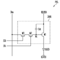
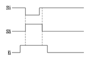
도 2는 누설전류를 최소화하기 위한 본 발명의 실시예에 의한 트랜지스터들의 접속관계를 나타내는 도면이다. 도 2에 도시된 트랜지스터들은 화소(PXL)에 포함되며, 전류의 누설경로에 위치된다.2 is a diagram showing a connection relation of transistors according to an embodiment of the present invention for minimizing a leakage current. The transistors shown in Fig. 2 are included in the pixel PXL and are located in the leakage path of the current.
도 2를 참조하면, 본 발명의 실시예에 의한 화소(PXL)의 전류 누설경로에는 산화물 반도체 트랜지스터(M(O)) 및 폴리 실리콘 반도체 트랜지스터(M(P))가 형성된다. 일례로, 구동 트랜지스터(MD)의 게이트전극에 접속되도록 폴리 실리콘 반도체 트랜지스터(M(P))가 형성되고, 폴리 실리콘 반도체 트랜지스터(M(P))와 접속되도록 산화물 반도체 트랜지스터(M(O))가 형성될 수 있다.Referring to FIG. 2, an oxide semiconductor transistor M (O) and a polysilicon semiconductor transistor M (P) are formed in a current leakage path of a pixel PXL according to an embodiment of the present invention. For example, the polysilicon semiconductor transistor M (P) is formed so as to be connected to the gate electrode of the driving transistor MD and the oxide semiconductor transistor M (O) is connected to the polysilicon semiconductor transistor M (P) Can be formed.
산화물 반도체 트랜지스터(M(O))는 게이트전극, 소스전극 및 드레인전극을 포함하며, 액티브층이 산화물 반도체로 형성된다. 여기서, 산화물 반도체는 비정질 또는 결정질로 설정될 수 있다. 산화물 반도체 트랜지스터(M(O))는 N타입 트랜지스터로 형성될 수 있다.The oxide semiconductor transistor M (O) includes a gate electrode, a source electrode, and a drain electrode, and the active layer is formed of an oxide semiconductor. Here, the oxide semiconductor may be set to amorphous or crystalline. The oxide semiconductor transistor M (O) may be formed of an N-type transistor.
산화물 반도체 트랜지스터(M(O))는 저온 공정이 가능하며, 폴리 실리콘 반도체 트랜지스터(M(P))에 비하여 낮은 전하 이동도를 갖는다. 이와 같은 산화물 반도체 트랜지스터(M(O))는 오프 전류 특성이 우수하다.The oxide semiconductor transistor M (O) is capable of a low temperature process and has a lower charge mobility than the polysilicon semiconductor transistor M (P). Such an oxide semiconductor transistor M (O) has excellent off current characteristics.
폴리 실리콘 반도체 트랜지스터(M(P))는 게이트전극, 소스전극 및 드레인전극을 포함하며, 액티브층이 폴리 실리콘으로 형성된다. 일례로, 폴리 실리콘 반도체 트랜지스터(M(P))는 LTPS(Low Temperature Poly-Silicon) 트랜지스터로 설정될 수 있다. 이와 같은 폴리 실리콘 반도체 트랜지스터(M(P))는 P타입 또는 N타입 트랜지스터로 형성될 수 있다. 다만, 도 2에서는 설명의 편의성을 위하여 폴리 실리콘 반도체 트랜지스터(M(P))를 P타입 트랜지스터로 도시하였다. 폴리 실리콘 반도체 트랜지스터(M(P))는 높은 전자 이동도를 가지며, 이에 따라 빠른 구동 특성을 갖는다. The polysilicon semiconductor transistor M (P) includes a gate electrode, a source electrode, and a drain electrode, and the active layer is formed of polysilicon. For example, the polysilicon semiconductor transistor M (P) may be configured as a Low Temperature Poly-Silicon (LTPS) transistor. Such a polysilicon semiconductor transistor M (P) may be formed of a P type or N type transistor. However, in FIG. 2, the polysilicon semiconductor transistor M (P) is shown as a P-type transistor for ease of explanation. The polysilicon semiconductor transistor M (P) has a high electron mobility and thus has a fast driving characteristic.
폴리 실리콘 반도체 트랜지스터(M(P))의 제 1전극은 구동 트랜지스터(MD)의 게이트전극에 접속되고, 제 2전극은 산화물 반도체 트랜지스터(M(O))의 제 1전극에 접속된다. 그리고, 폴리 실리콘 반도체 트랜지스터(M(P))의 게이트전극은 제 1주사선(S1)에 접속된다. 이와 같은 폴리 실리콘 반도체 트랜지스터(M(P))는 제 1주사선(S1)으로 제 1주사신호가 공급될 때 턴-온된다.The first electrode of the polysilicon semiconductor transistor M (P) is connected to the gate electrode of the driving transistor MD, and the second electrode thereof is connected to the first electrode of the oxide semiconductor transistor M (O). The gate electrode of the polysilicon semiconductor transistor M (P) is connected to the first scanning line S1. The polysilicon semiconductor transistor M (P) is turned on when the first scan signal is supplied to the first scan line S1.
산화물 반도체 트랜지스터(M(O))의 제 1전극은 폴리 실리콘 반도체 트랜지스터(M(P))의 제 2전극에 접속된다. 그리고, 산화물 반도체 트랜지스터(M(O))의 게이트전극은 제 2주사선(S2)에 접속된다. 이와 같은 산화물 반도체 트랜지스터(M(O))는 제 2주사선(S2)으로 제 2주사신호가 공급될 때 턴-온된다.The first electrode of the oxide semiconductor transistor M (O) is connected to the second electrode of the polysilicon semiconductor transistor M (P). The gate electrode of the oxide semiconductor transistor M (O) is connected to the second scanning line S2. The oxide semiconductor transistor M (O) is turned on when the second scan signal is supplied to the second scan line S2.
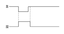
여기서, 폴리 실리콘 반도체 트랜지스터(M(P)) 및 산화물 반도체 트랜지스터(M(O))는 턴-온기간이 중첩되며, 폴리 실리콘 반도체 트랜지스터(M(P))는 산화물 반도체 트랜지스터(M(O))보다 먼저 턴-오프된다.The turn-on period of the polysilicon semiconductor transistor M (P) and the oxide semiconductor transistor M (O) overlap, and the polysilicon semiconductor transistor M (P) ).
이를 위하여, 제 1주사선(S1)으로 공급되는 제 1주사신호 및 제 2주사선(S2)으로 공급되는 제 2주사신호는 도 3에 도시된 바와 같이 동시에 공급될 수 있다. 이 경우, 폴리 실리콘 반도체 트랜지스터(M(P)) 및 산화물 반도체 트랜지스터(M(O))는 동시에 턴-온된다. 산화물 반도체 트랜지스터(M(O))가 폴리 실리콘 반도체 트랜지스터(M(P))와 동시에 턴-온되면 폴리 실리콘 반도체 트랜지스터(M(P))의 빠른 구동 특성을 확보할 수 있다.For this, a first scan signal supplied to the first scan line S1 and a second scan signal supplied to the second scan line S2 may be simultaneously supplied as shown in FIG. In this case, the polysilicon semiconductor transistor M (P) and the oxide semiconductor transistor M (O) are simultaneously turned on. When the oxide semiconductor transistor M (O) is turned on simultaneously with the polysilicon semiconductor transistor M (P), fast driving characteristics of the polysilicon semiconductor transistor M (P) can be ensured.
한편, 제 1주사선(S1)으로 제 1주사신호의 공급이 중단된 후 제 2주사선(S2)으로 제 2주사신호의 공급이 중단된다. 그러면, 폴리 실리콘 반도체 트랜지스터(M(P))가 턴-오프된 후 산화물 반도체 트랜지스터(M(O))가 턴-오프된다. 폴리 실리콘 반도체 트랜지스터(M(P))가 산화물 반도체 트랜지스터(M(O))보다 먼저 턴-오프되면 구동 트랜지스터(MD)의 게이트전극 전압 변화를 최소화할 수 있고, 이에 따라 화질이 저하되는 것을 방지할 수 있다.On the other hand, after the supply of the first scan signal to the first scan line S1 is stopped, the supply of the second scan signal to the second scan line S2 is interrupted. Then, the oxide semiconductor transistor M (O) is turned off after the polysilicon semiconductor transistor M (P) is turned off. When the polysilicon semiconductor transistor M (P) is turned off prior to the oxide semiconductor transistor M (O), a change in the gate electrode voltage of the driving transistor MD can be minimized, can do.
상세히 설명하면, 산화물 반도체 트랜지스터(M(O))의 채널 커패시터의 용량은 폴리 실리콘 반도체 트랜지스터(M(P))의 채널 커패시터의 용량보다 크게 설정된다. 따라서, 폴리 실리콘 반도체 트랜지스터(M(P)) 및 산화물 반도체 트랜지스터(M(O))가 동시에 턴-오프되면 산화물 반도체 트랜지스터(M(O))의 킥백 전압에 의하여 구동 트랜지스터(MD)의 게이트전극 전압이 소정 전압만큼 변동될 수 있고, 이에 따라 화질이 저하될 수 있다.More specifically, the capacitance of the channel capacitor of the oxide semiconductor transistor M (O) is set to be larger than the capacitance of the channel capacitor of the polysilicon semiconductor transistor M (P). Therefore, when the polysilicon semiconductor transistor M (P) and the oxide semiconductor transistor M (O) are turned off at the same time, the gate electrode of the driving transistor MD is turned on by the kickback voltage of the oxide semiconductor transistor M (O) The voltage may fluctuate by a predetermined voltage, and the image quality may be deteriorated accordingly.
반면에, 본원 발명의 실시예와 같이 구동 트랜지스터(MD)의 게이트전극에 접속된 폴리 실리콘 반도체 트랜지스터(M(P))를 턴-오프한 후, 산화물 반도체 트랜지스터(M(O))를 턴-오프시키면 산화물 반도체 트랜지스터(M(O))의 채널 커패시터에 의하여 구동 트랜지스터(MD)의 게이트전극 전압이 변경되는 것을 방지할 수 있다. 추가적으로, 산화물 반도체 트랜지스터(M(O))가 턴-오프되면 누설경로에서 흐르는 누설전류를 최소화할 수 있다.On the other hand, after the polysilicon semiconductor transistor M (P) connected to the gate electrode of the driving transistor MD is turned off as in the embodiment of the present invention, the oxide semiconductor transistor M (O) It is possible to prevent the gate electrode voltage of the driving transistor MD from being changed by the channel capacitor of the oxide semiconductor transistor M (O). In addition, when the oxide semiconductor transistor M (O) is turned off, the leakage current flowing in the leakage path can be minimized.
즉, 본 발명의 실시예에서는 화소(PXL)의 누설경로에 산화물 반도체 트랜지스터(M(O)) 및 폴리 실리콘 반도체 트랜지스터(M(P))를 형성하며, 산화물 반도체 트랜지스터(M(O))를 이용하여 누설경로에서 흐르는 누설전류를 최소화한다. 누설경로에서 흐르는 누설전류가 최소화되는 경우, 화소(PXL)에서 원하는 휘도의 영상을 표시할 수 있다.That is, in the embodiment of the present invention, the oxide semiconductor transistor M (O) and the polysilicon semiconductor transistor M (P) are formed in the leakage path of the pixel PXL and the oxide semiconductor transistor M (O) To minimize the leakage current flowing in the leakage path. When the leakage current flowing in the leakage path is minimized, the image of the desired luminance can be displayed in the pixel PXL.
추가적으로, 구동 트랜지스터(MD)의 게이트전극에 접속된 폴리 실리콘 반도체 트랜지스터(M(P))를 턴-오프한 후, 산화물 반도체 트랜지스터(M(O))를 턴-오프시킴으로서 구동 트랜지스터(MD)의 게이트전극 전압 변경을 최소화할 수 있다.In addition, after the polysilicon semiconductor transistor M (P) connected to the gate electrode of the driving transistor MD is turned off, the oxide semiconductor transistor M (O) is turned off, The gate electrode voltage change can be minimized.
도 4는 본 발명의 실시예에 의한 화소를 나타내는 도면이다. 도 4에서는 설명의 편의성을 위하여 i번째 수평라인에 위치되며, 제 m데이터선(Dm)과 접속된 화소(PXL)를 도시하기로 한다.4 is a view showing a pixel according to an embodiment of the present invention. 4, the pixel PXL is connected to the m-th data line Dm and is located on the i-th horizontal line for convenience of explanation.
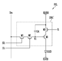
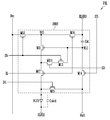
도 4를 참조하면, 본 발명의 실시예에 의한 화소(PXL)는 유기 발광 다이오드(OLED)와, 유기 발광 다이오드(OLED)로 공급되는 전류량을 제어하기 위한 화소회로(2001)를 구비한다.Referring to FIG. 4, a pixel PXL according to an embodiment of the present invention includes an organic light emitting diode OLED and a
유기 발광 다이오드(OLED)의 애노드전극은 화소회로(2001)에 접속되고, 캐소드전극은 제 2구동전원(ELVSS)에 접속된다. 이와 같은 유기 발광 다이오드(OLED)는 화소회로(2001)로부터 공급되는 전류량에 대응하여 소정 휘도의 빛을 생성한다.The anode electrode of the organic light emitting diode OLED is connected to the
화소회로(2001)는 데이터신호에 대응하여 제 1구동전원(ELVDD)으로부터 유기 발광 다이오드(OLED)를 경유하여 제 2구동전원(ELVSS)으로 흐르는 전류량을 제어한다. 이를 위하여, 화소회로(2001)는 제 1트랜지스터(M1), 제 2트랜지스터(M2), 보조 트랜지스터(MS) 및 스토리지 커패시터(Cst)를 구비한다.The
제 1트랜지스터(M1 : 구동 트랜지스터)의 제 1전극은 제 1구동전원(ELVDD)에 접속되고, 제 2전극은 유기 발광 다이오드(OLED)의 애노드전극에 접속된다. 그리고, 제 1트랜지스터(M1)의 게이트전극은 제 1노드(N1)에 접속된다. 이와 같은 제 1트랜지스터(M1)는 제 1노드(N1)의 전압에 대응하여 제 1구동전원(ELVDD)으로부터 유기 발광 다이오드(OLED)를 경유하여 제 2구동전원(ELVSS)으로 흐르는 전류량을 제어한다.The first electrode of the first transistor M1 (the driving transistor) is connected to the first driving power source ELVDD, and the second electrode thereof is connected to the anode electrode of the organic light emitting diode OLED. The gate electrode of the first transistor M1 is connected to the first node N1. The first transistor M1 controls the amount of current flowing from the first driving power ELVDD to the second driving power ELVSS via the organic light emitting diode OLED in response to the voltage of the first node N1 .
제 2트랜지스터(M2)는 제 1노드(N1)와 보조 트랜지스터(MS) 사이에 접속된다. 그리고, 제 2트랜지스터(M2)의 게이트전극은 i번째 제 1주사선(S1i)에 접속된다. 이와 같은 제 2트랜지스터(M2)는 i번째 제 1주사선(S1i)으로 제 1주사신호가 공급될 때 턴-온되어 보조 트랜지스터(MS)와 제 1노드(N1)를 전기적으로 접속시킨다.The second transistor M2 is connected between the first node N1 and the auxiliary transistor MS. The gate electrode of the second transistor M2 is connected to the i-th first scanning line S1i. The second transistor M2 is turned on when the first scan signal is supplied to the i-th first scan line S1i to electrically connect the auxiliary transistor MS and the first node N1.
보조 트랜지스터(MS)는 데이터선(Dm)과 제 2트랜지스터(M2) 사이에 접속된다. 그리고, 보조 트랜지스터(MS)의 게이트전극은 i번째 제 2주사선(S2i)에 접속된다. 이와 같은 보조 트랜지스터(MS)는 i번째 제 2주사선(S2i)으로 제 2주사신호가 공급될 때 턴-온되어 데이터선(Dm)과 제 2트랜지스터(M2)를 전기적으로 접속시킨다.The auxiliary transistor MS is connected between the data line Dm and the second transistor M2. The gate electrode of the auxiliary transistor MS is connected to the i-th second scanning line S2i. The auxiliary transistor MS is turned on when the second scan signal is supplied to the i-th second scan line S2i to electrically connect the data line Dm and the second transistor M2.
스토리지 커패시터(Cst)는 제 1노드(N1)와 제 1구동전원(ELVDD) 사이에 접속된다. 이와 같은 스토리지 커패시터(Cst)는 데이터신호에 대응되는 전압을 저장한다.The storage capacitor Cst is connected between the first node N1 and the first drive power supply ELVDD. The storage capacitor Cst stores a voltage corresponding to the data signal.
한편, 상술한 제 1트랜지스터(M1) 및 제 2트랜지스터(M2)는 P타입의 폴리 실리콘 반도체 트랜지스터로 형성되고, 보조 트랜지스터(MS)는 N타입의 산화물 반도체 트랜지스터로 형성된다. 제 1트랜지스터(M1) 및 제 2트랜지스터(M2)가 폴리 실리콘 반도체 트랜지스터로 형성되면 빠른 구동 특성을 확보할 수 있다. 보조 트랜지스터(MS)가 산화물 반도체 트랜지스터로 형성되면 데이터선(Dm)과 제 1노드(N1) 사이의 누설전류가 최소화되고, 이에 따라 화소(PXL)에서 원하는 휘도의 영상을 구현할 수 있다.The first transistor M1 and the second transistor M2 are formed of a P type polysilicon semiconductor transistor and the auxiliary transistor MS is formed of an N type oxide semiconductor transistor. If the first transistor M1 and the second transistor M2 are formed of a polysilicon semiconductor transistor, fast driving characteristics can be secured. When the auxiliary transistor MS is formed of an oxide semiconductor transistor, a leakage current between the data line Dm and the first node N1 is minimized, thereby realizing an image of a desired luminance in the pixel PXL.
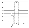
도 5는 도 4에 도시된 화소의 구동방법 실시예를 나타내는 파형도이다. 5 is a waveform diagram showing an embodiment of the driving method of the pixel shown in FIG.
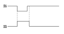
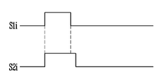
도 5를 참조하면, 먼저 제 i번째 제 1주사선(S1i)으로 제 1주사신호가 공급되고, i번째 제 2주사선(S2i)으로 제 2주사신호가 공급된다. 여기서, 제 1주사신호 및 제 2주사신호는 동시에 공급될 수 있다.Referring to FIG. 5, a first scan signal is supplied to an i-th first scan line S1i and a second scan signal is supplied to an i-th second scan line S2i. Here, the first scan signal and the second scan signal can be supplied simultaneously.
i번째 제 1주사선(S1i)으로 제 1주사신호가 공급되면 제 2트랜지스터(M2)가 턴-온된다. i번째 제 2주사선(S2i)으로 제 2주사신호가 공급되면 보조 트랜지스터(MS)가 턴-온된다. When the first scan signal is supplied to the i-th first scan line S1i, the second transistor M2 is turned on. When the second scan signal is supplied to the i-th second scan line S2i, the auxiliary transistor MS is turned on.
보조 트랜지스터(MS) 및 제 2트랜지스터(M2)가 턴-온되면 데이터선(Dm)과 제 1노드(N1)가 전기적으로 접속된다. 그러면, 데이터선(Dm)으로 공급된 데이터신호가 보조 트랜지스터(MS) 및 제 2트랜지스터(M2)를 경유하여 제 1노드(N1)로 공급된다. 이때, 스토리지 커패시터(Cst)는 데이터신호에 대응되는 전압을 저장한다.When the auxiliary transistor MS and the second transistor M2 are turned on, the data line Dm and the first node N1 are electrically connected. Then, the data signal supplied to the data line Dm is supplied to the first node N1 via the auxiliary transistor MS and the second transistor M2. At this time, the storage capacitor Cst stores a voltage corresponding to the data signal.
이후, i번째 제 1주사선(S1i)으로 제 1주사신호의 공급이 중단되고, 이에 따라 제 2트랜지스터(M2)가 턴-오프된다. 제 2트랜지스터(M2)가 턴-오프된 후 i번째 제 2주사선(S2i)으로 제 2주사신호의 공급이 중단되고, 이에 따라 보조 트랜지스터(MS)가 턴-오프된다. 이때, 제 2트랜지스터(M2)가 턴-오프 상태로 설정되기 때문에 산화물 반도체 트랜지스터로 형성된 보조 트랜지스터(MS)의 채널 커패시터에 의하여 제 1노드(N1)의 전압이 변경되는 것을 방지할 수 있다.Thereafter, the supply of the first scan signal to the i-th first scan line S1i is stopped, and the second transistor M2 is turned off accordingly. After the second transistor M2 is turned off, the supply of the second scan signal to the i-th second scan line S2i is stopped, and the auxiliary transistor MS is turned off. At this time, since the second transistor M2 is set in the turn-off state, the voltage of the first node N1 can be prevented from being changed by the channel capacitor of the auxiliary transistor MS formed of the oxide semiconductor transistor.
보조 트랜지스터(MS)가 턴-오프된 후 제 1트랜지스터(M1)는 제 1노드(N1)의 전압에 대응하여 제 1구동전원(ELVDD)으로부터 유기 발광 다이오드(OLED)를 경유하여 제 2구동전원(ELVSS)으로 흐르는 전류량을 제어한다. 그러면, 유기 발광 다이오드(OLED)는 제 1트랜지스터(M1)로부터 공급되는 전류량에 대응하여 소정 휘도의 빛을 생성한다.After the auxiliary transistor MS is turned off, the first transistor M1 is turned off from the first driving power source ELVDD via the organic light emitting diode OLED in response to the voltage of the first node N1, (ELVSS). Then, the organic light emitting diode OLED generates light having a predetermined luminance corresponding to the amount of current supplied from the first transistor M1.
추가적으로, 유기 발광 다이오드(OLED)가 발광될 때 보조 트랜지스터(MS)는 턴-오프 상태로 설정된다. 산화물 반도체 트랜지스터로 형성된 보조 트랜지스터(MS)가 턴-오프되면 데이터선(Dm)과 제 1노드(N1) 사이의 누설전류가 최소화되고, 이에 따라 원하는 휘도의 영상을 표시할 수 있다.In addition, the auxiliary transistor MS is set to the turn-off state when the organic light emitting diode OLED emits light. When the auxiliary transistor MS formed of the oxide semiconductor transistor is turned off, the leakage current between the data line Dm and the first node N1 is minimized, thereby displaying an image with a desired luminance.
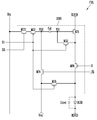
도 6a 및 도 6b는 본 발명의 다른 실시예에 의한 화소를 나타내는 도면이다. 도 6a 및 도 6b를 설명할 때 도 4와 동일한 구성에 대해서는 동일한 도면부호를 할당함과 아울러 상세한 설명은 생략하기로 한다.6A and 6B are views showing pixels according to another embodiment of the present invention. 6A and 6B, the same reference numerals are assigned to the same components as those in FIG. 4, and a detailed description thereof will be omitted.
도 6a를 참조하면, 본 발명의 다른 실시예에 의한 화소는 유기 발광 다이오드(OLED)와, 유기 발광 다이오드(OLED)로 공급되는 전류량을 제어하기 위한 화소회로(2001')를 구비한다.Referring to FIG. 6A, a pixel according to another embodiment of the present invention includes an organic light emitting diode (OLED) and a pixel circuit 2001 'for controlling an amount of current supplied to the organic light emitting diode (OLED).
유기 발광 다이오드(OLED)의 애노드전극은 화소회로(2001')에 접속되고, 캐소드전극은 제 2구동전원(ELVSS)에 접속된다. 이와 같은 유기 발광 다이오드(OLED)는 화소회로(2001')로부터 공급되는 전류량에 대응하여 소정 휘도의 빛을 생성한다.The anode electrode of the organic light emitting diode OLED is connected to the pixel circuit 2001 ', and the cathode electrode thereof is connected to the second driving power source ELVSS. The organic light emitting diode OLED generates light having a predetermined luminance corresponding to the amount of current supplied from the pixel circuit 2001 '.
화소회로(2001')는 데이터신호에 대응하여 제 1구동전원(ELVDD)으로부터 유기 발광 다이오드(OLED)를 경유하여 제 2구동전원(ELVSS)으로 흐르는 전류량을 제어한다. 이를 위하여, 화소회로(2001')는 제 1트랜지스터(M1) 내지 제 3트랜지스터(M3), 보조 트랜지스터(MS) 및 스토리지 커패시터(Cst)를 구비한다.The pixel circuit 2001 'controls the amount of current flowing from the first driving power ELVDD to the second driving power ELVSS via the organic light emitting diode OLED in response to the data signal. To this end, the pixel circuit 2001 'includes a first transistor M1 through a third transistor M3, an auxiliary transistor MS, and a storage capacitor Cst.
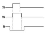
제 3트랜지스터(M3)는 제 1구동전원(ELVDD)과 제 1트랜지스터(M1)의 제 1전극 사이에 위치된다. 그리고, 제 3트랜지스터(M3)의 게이트전극은 i번째 발광 제어선(Ei)에 접속된다. 이와 같은 제 3트랜지스터(M3)는 i번째 발광 제어선(Ei)으로 발광 제어신호가 공급될 때 턴-오프되고, i번째 발광 제어선(Ei)으로 발광 제어신호가 공급되지 않을 때 턴-온된다.The third transistor M3 is located between the first driving power source ELVDD and the first electrode of the first transistor M1. The gate electrode of the third transistor M3 is connected to the i-th emission control line Ei. The third transistor M3 is turned off when the emission control signal is supplied to the i-th emission control line Ei and turned on when the emission control signal is not supplied to the i-th emission control line Ei. do.
여기서, i번째 발광 제어선(Ei)으로 공급되는 발광 제어신호는 도 7에 도시된 바와 같이 i번째 제 1주사선(S1i)으로 공급되는 제 1주사신호 및 i번째 제 2주사선(S2i)으로 공급되는 제 2주사신호와 중첩된다. 따라서, 제 3트랜지스터(M3)는 스토리지 커패시터(Cst)에 데이터신호에 대응되는 전압이 저장될 때 턴-오프되고, 이에 따라 유기 발광 다이오드(OLED)가 불필요하게 발광되는 것을 방지할 수 있다.Here, the emission control signal supplied to the i-th emission control line Ei is supplied to the first scan signal supplied to the i-th first scan line S1i and the i-th second scan line S2i as shown in FIG. Is overlapped with the second scanning signal. Therefore, the third transistor M3 is turned off when the voltage corresponding to the data signal is stored in the storage capacitor Cst, thereby preventing the organic light emitting diode OLED from being unnecessarily emitted.
추가적으로, 제 1주사신호 및 제 2주사신호는 게이트 온 전압으로 설정된다. 일례로, 제 1주사선(S1i)으로 공급되는 제 1주사신호는 제 2트랜지스터(M2)가 턴-온될 수 있도록 게이트 온 전압인 로우전압으로 설정될 수 있다. 또한, 제 1주사선(S1i)으로 제 1주사신호가 공급되지 않을 때 제 1주사선(S1i)으로는 게이트 오프 전압인 하이전압이 공급될 수 있다.In addition, the first scan signal and the second scan signal are set to the gate-on voltage. For example, the first scan signal supplied to the first scan line S1i may be set to a low voltage, which is a gate-on voltage, so that the second transistor M2 may be turned on. In addition, when the first scan signal is not supplied to the first scan line S1i, a high voltage which is a gate off voltage may be supplied to the first scan line S1i.
마찬가지로, 제 2주사선(S2i)으로 공급되는 제 2주사신호는 보조 트랜지스터(MS)가 턴-온될 수 있도록 게이트 온 전압인 하이전압으로 설정될 수 있다. 그리고, 제 2주사선(S2i)으로 제 2주사신호가 공급되지 않을 때 제 2주사선(S2i)으로는 게이트 오프 전압인 로우전압이 공급될 수 있다.Similarly, the second scan signal supplied to the second scan line S2i may be set to a high voltage which is a gate-on voltage so that the auxiliary transistor MS can be turned on. When the second scan signal is not supplied to the second scan line S2i, a low voltage which is a gate off voltage may be supplied to the second scan line S2i.
추가적으로, 발광 제어신호는 게이트 오프 전압으로 설정된다. 일례로, 발광 제어선(Ei)으로 공급되는 발광 제어신호는 제 3트랜지스터(M3)가 턴-오프되도록 게이트 오프 전압인 하이전압으로 설정될 수 있다. 그리고, 발광 제어선(Ei)으로 발광 제어신호가 공급되지 않을 때 발광 제어선(Ei)으로는 게이트 온 전압인 로우전압이 공급될 수 있다.In addition, the emission control signal is set to the gate off voltage. For example, the emission control signal supplied to the emission control line Ei may be set to a high voltage which is a gate-off voltage so that the third transistor M3 is turned off. When the emission control signal is not supplied to the emission control line Ei, a low voltage which is a gate-on voltage can be supplied to the emission control line Ei.
도 6b를 참조하면, 본 발명의 다른 실시예에 의한 화소는 유기 발광 다이오드(OLED)와, 유기 발광 다이오드(OLED)로 공급되는 전류량을 제어하기 위한 화소회로(2001')를 구비한다.Referring to FIG. 6B, a pixel according to another embodiment of the present invention includes an organic light emitting diode (OLED) and a pixel circuit 2001 'for controlling the amount of current supplied to the organic light emitting diode (OLED).
유기 발광 다이오드(OLED)의 애노드전극은 화소회로(2001')에 접속되고, 캐소드전극은 제 2구동전원(ELVSS)에 접속된다. 이와 같은 유기 발광 다이오드(OLED)는 화소회로(2001')로부터 공급되는 전류량에 대응하여 소정 휘도의 빛을 생성한다.The anode electrode of the organic light emitting diode OLED is connected to the pixel circuit 2001 ', and the cathode electrode thereof is connected to the second driving power source ELVSS. The organic light emitting diode OLED generates light having a predetermined luminance corresponding to the amount of current supplied from the pixel circuit 2001 '.
화소회로(2001')는 데이터신호에 대응하여 제 1구동전원(ELVDD)으로부터 유기 발광 다이오드(OLED)를 경유하여 제 2구동전원(ELVSS)으로 흐르는 전류량을 제어한다. 이를 위하여, 화소회로(2001')는 제 1트랜지스터(M1) 내지 제 3트랜지스터(M3), 보조 트랜지스터(MS) 및 스토리지 커패시터(Cst)를 구비한다.The pixel circuit 2001 'controls the amount of current flowing from the first driving power ELVDD to the second driving power ELVSS via the organic light emitting diode OLED in response to the data signal. To this end, the pixel circuit 2001 'includes a first transistor M1 through a third transistor M3, an auxiliary transistor MS, and a storage capacitor Cst.
제 3트랜지스터(M3)는 제 1트랜지스터(M1)의 제 2전극과 유기 발광 다이오드(OLED)의 애노드전극 사이에 접속된다. 그리고, 제 3트랜지스터(M3)의 게이트전극은 i번째 발광 제어선(Ei)에 접속된다. 이와 같은 제 3트랜지스터(M3)는 i번째 발광 제어선(Ei)으로 발광 제어신호가 공급될 때 턴-오프되고, i번째 발광 제어선(Ei)으로 발광 제어신호가 공급되지 않을 때 턴-온된다.The third transistor M3 is connected between the second electrode of the first transistor M1 and the anode electrode of the organic light emitting diode OLED. The gate electrode of the third transistor M3 is connected to the i-th emission control line Ei. The third transistor M3 is turned off when the emission control signal is supplied to the i-th emission control line Ei and turned on when the emission control signal is not supplied to the i-th emission control line Ei. do.
여기서, i번째 발광 제어선(Ei)으로 공급되는 발광 제어신호는 도 7에 도시된 바와 같이 i번째 제 1주사선(S1i)으로 공급되는 제 1주사신호 및 i번째 제 2주사선(S2i)으로 공급되는 제 2주사신호와 중첩된다. 따라서, 제 3트랜지스터(M3)는 스토리지 커패시터(Cst)에 데이터신호에 대응되는 전압이 저장될 때 턴-오프되고, 이에 따라 유기 발광 다이오드(OLED)가 불필요하게 발광되는 것을 방지할 수 있다.Here, the emission control signal supplied to the i-th emission control line Ei is supplied to the first scan signal supplied to the i-th first scan line S1i and the i-th second scan line S2i as shown in FIG. Is overlapped with the second scanning signal. Therefore, the third transistor M3 is turned off when the voltage corresponding to the data signal is stored in the storage capacitor Cst, thereby preventing the organic light emitting diode OLED from being unnecessarily emitted.
도 8은 본 발명의 또 다른 실시예에 의한 화소를 나타내는 도면이다. 도 8에서는 설명의 편의성을 위하여 i번째 수평라인에 위치되며, 제 m데이터선(Dm)과 접속된 화소(PXL)를 도시하기로 한다. 도 8을 설명할 때 도 4와 동일한 기능을 수행하는 보조 트랜지스터(MS)는 동일한 도면부호를 할당하기로 한다.8 is a view showing a pixel according to another embodiment of the present invention. 8, a pixel PXL which is located on the i-th horizontal line and connected to the m-th data line Dm is shown for convenience of explanation. In describing FIG. 8, auxiliary transistors MS performing the same function as FIG. 4 are assigned the same reference numerals.
도 8을 참조하면, 본 발명의 또 다른 실시예에 의한 화소는 유기 발광 다이오드(OLED)와, 유기 발광 다이오드(OLED)로 공급되는 전류량을 제어하기 위한 화소회로(2002)를 구비한다.Referring to FIG. 8, a pixel according to another embodiment of the present invention includes an organic light emitting diode (OLED) and a
유기 발광 다이오드(OLED)의 애노드전극은 화소회로(2002)에 접속되고, 캐소드전극은 제 2구동전원(ELVSS)에 접속된다. 이와 같은 유기 발광 다이오드(OLED)는 화소회로(2002)로부터 공급되는 전류량에 대응하여 소정 휘도의 빛을 생성한다.The anode electrode of the organic light emitting diode (OLED) is connected to the
화소회로(2002)는 데이터신호에 대응하여 제 1구동전원(ELVDD)으로부터 유기 발광 다이오드(OLED)를 경유하여 제 2구동전원(ELVSS)으로 흐르는 전류량을 제어한다. 이를 위하여, 화소회로(2002)는 제 1트랜지스터(M1'), 제 2트랜지스터(M2'), 보조 트랜지스터(MS) 및 스토리지 커패시터(Cst')를 구비한다.The
제 1트랜지스터(M1' : 구동 트랜지스터)의 제 1전극은 제 1구동전원(ELVDD)에 접속되고, 제 2전극은 유기 발광 다이오드(OLED)의 애노드전극에 접속된다. 그리고, 제 1트랜지스터(M1')의 게이트전극은 제 1노드(N1')에 접속된다. 이와 같은 제 1트랜지스터(M1')는 제 1노드(N1')의 전압에 대응하여 제 1구동전원(ELVDD)으로부터 유기 발광 다이오드(OLED)를 경유하여 제 2구동전원(ELVSS)으로 흐르는 전류량을 제어한다.A first electrode of the first transistor M1 '(driving transistor) is connected to the first driving power source ELVDD, and a second electrode thereof is connected to the anode electrode of the organic light emitting diode OLED. The gate electrode of the first transistor M1 'is connected to the first node N1'. The first transistor M1 'has a current amount flowing from the first driving power source ELVDD to the second driving power source ELVSS via the organic light emitting diode OLED corresponding to the voltage of the first node N1' .
제 2트랜지스터(M2')는 제 1노드(N1')와 보조 트랜지스터(MS) 사이에 접속된다. 그리고, 제 2트랜지스터(M2')의 게이트전극은 i번째 제 1주사선(S1i)에 접속된다. 이와 같은 제 2트랜지스터(M2')는 i번째 제 1주사선(S1i)으로 제 1주사신호가 공급될 때 턴-온되어 보조 트랜지스터(MS)와 제 1노드(N1')를 전기적으로 접속시킨다.The second transistor M2 'is connected between the first node N1' and the auxiliary transistor MS. The gate electrode of the second transistor M2 'is connected to the i-th first scanning line S1i. The second transistor M2 'is turned on when the first scan signal is supplied to the i-th first scan line S1i to electrically connect the auxiliary transistor MS and the first node N1'.
보조 트랜지스터(MS)는 데이터선(Dm)과 제 2트랜지스터(M2') 사이에 접속된다. 그리고, 보조 트랜지스터(MS)의 게이트전극은 i번째 제 2주사선(S2i)에 접속된다. 이와 같은 보조 트랜지스터(MS)는 i번째 제 2주사선(S2i)으로 주사신호가 공급될 때 턴-온되어 데이터선(Dm)과 제 2트랜지스터(M2')를 전기적으로 접속시킨다.The auxiliary transistor MS is connected between the data line Dm and the second transistor M2 '. The gate electrode of the auxiliary transistor MS is connected to the i-th second scanning line S2i. The auxiliary transistor MS is turned on when a scan signal is supplied to the i-th second scan line S2i to electrically connect the data line Dm and the second transistor M2 '.
스토리지 커패시터(Cst')는 제 1노드(N1')와 유기 발광 다이오드(OLED)의 애노드전극(즉, 제 2노드(N2)) 사이에 접속된다. 이와 같은 스토리지 커패시터(Cst')는 데이터신호에 대응되는 전압을 저장한다.The storage capacitor Cst 'is connected between the first node N1' and the anode electrode (that is, the second node N2) of the organic light emitting diode OLED. Such a storage capacitor Cst 'stores a voltage corresponding to the data signal.
한편, 상술한 제 1트랜지스터(M1) 및 제 2트랜지스터(M2)는 N타입의 폴리 실리콘 반도체 트랜지스터로 형성되고, 보조 트랜지스터(MS)는 N타입의 산화물 반도체 트랜지스터로 형성된다. 제 1트랜지스터(M1) 및 제 2트랜지스터(M2)가 폴리 실리콘 반도체 트랜지스터로 형성되면 빠른 구동 특성을 확보할 수 있다. 보조 트랜지스터(MS)가 산화물 반도체 트랜지스터로 형성되면 데이터선(Dm)과 제 1노드(N1') 사이의 누설전류가 최소화되고, 이에 따라 화소(PXL)에서 원하는 휘도의 영상을 구현할 수 있다.The first transistor M1 and the second transistor M2 are formed of an N type polysilicon semiconductor transistor and the auxiliary transistor MS is formed of an N type oxide semiconductor transistor. If the first transistor M1 and the second transistor M2 are formed of a polysilicon semiconductor transistor, fast driving characteristics can be secured. If the auxiliary transistor MS is formed of an oxide semiconductor transistor, the leakage current between the data line Dm and the first node N1 'is minimized, thereby realizing an image of a desired luminance in the pixel PXL.
한편, 도 8에 도시된 화소(PXL)는 도 4에 도시된 화소(PXL)와 비교하여 제 1트랜지스터(M1') 및 제 2트랜지스터(M2')가 N타입 트랜지스터로 설정될 뿐, 그 외의 동작은 실질적으로 동일하다.The pixel PXL shown in FIG. 8 is different from the pixel PXL shown in FIG. 4 in that the first transistor M1 'and the second transistor M2' The operation is substantially the same.
도 9는 도 8에 도시된 화소의 구동방법 실시예를 나타내는 파형도이다.Fig. 9 is a waveform diagram showing an embodiment of the driving method of the pixel shown in Fig. 8. Fig.
도 9를 참조하면, 먼저 제 i번째 제 1주사선(S1i)으로 제 1주사신호가 공급되고, i번째 제 2주사선(S2i)으로 제 2주사신호가 공급된다. 여기서, 제 1주사신호 및 제 2주사신호는 동시에 공급될 수 있다.Referring to FIG. 9, a first scan signal is supplied to the i-th first scan line S1i and a second scan signal is supplied to the i-th second scan line S2i. Here, the first scan signal and the second scan signal can be supplied simultaneously.
i번째 제 1주사선(S1i)으로 제 1주사신호가 공급되면 제 2트랜지스터(M2')가 턴-온된다. i번째 제 2주사선(S2i)으로 제 2주사신호가 공급되면 보조 트랜지스터(MS)가 턴-온된다.When the first scan signal is supplied to the i-th first scan line S1i, the second transistor M2 'is turned on. When the second scan signal is supplied to the i-th second scan line S2i, the auxiliary transistor MS is turned on.
보조 트랜지스터(MS) 및 제 2트랜지스터(M2')가 턴-온되면 데이터선(Dm)과 제 1노드(N1')가 전기적으로 접속된다. 그러면, 데이터선(Dm)으로 공급된 데이터신호가 보조 트랜지스터(MS) 및 제 2트랜지스터(M2')를 경유하여 제 1노드(N1')로 공급된다. 이때, 스토리지 커패시터(Cst')는 데이터신호에 대응되는 전압을 저장한다.When the auxiliary transistor MS and the second transistor M2 'are turned on, the data line Dm and the first node N1' are electrically connected. Then, the data signal supplied to the data line Dm is supplied to the first node N1 'via the auxiliary transistor MS and the second transistor M2'. At this time, the storage capacitor Cst 'stores the voltage corresponding to the data signal.
이후, i번째 제 1주사선(S1i)으로 제 1주사신호의 공급이 중단되고, 이에 따라 제 2트랜지스터(M2')가 턴-오프된다. 제 2트랜지스터(M2')가 턴-오프된 후 i번째 제 2주사선(S2i)으로 제 2주사신호의 공급이 중단되고, 이에 따라 보조 트랜지스터(MS)가 턴-오프된다. 이때, 제 2트랜지스터(M2')가 턴-오프 상태로 설정되기 때문에 산화물 반도체 트랜지스터로 형성된 보조 트랜지스터(MS)의 채널 커패시터에 의하여 제 1노드(N1')의 전압이 변경되는 것을 방지할 수 있다.Thereafter, the supply of the first scan signal to the i-th first scan line S1i is stopped, and the second transistor M2 'is turned off accordingly. After the second transistor M2 'is turned off, the supply of the second scan signal to the i-th second scan line S2i is stopped, and the auxiliary transistor MS is turned off. At this time, since the second transistor M2 'is set in the turn-off state, it is possible to prevent the voltage of the first node N1' from being changed by the channel capacitor of the auxiliary transistor MS formed of the oxide semiconductor transistor .
보조 트랜지스터(MS)가 턴-오프된 후 제 1트랜지스터(M1')는 제 1노드(N1')의 전압에 대응하여 제 1구동전원(ELVDD)으로부터 유기 발광 다이오드(OLED)를 경유하여 제 2구동전원(ELVSS)으로 흐르는 전류량을 제어한다. 그러면, 유기 발광 다이오드(OLED)는 제 1트랜지스터(M1')로부터 공급되는 전류량에 대응하여 소정 휘도의 빛을 생성한다.After the auxiliary transistor MS is turned off, the first transistor M1 'is turned off from the first driving power source ELVDD in response to the voltage of the first node N1' via the organic light emitting diode OLED, And controls the amount of current flowing in the driving power supply ELVSS. Then, the organic light emitting diode OLED generates light of a predetermined luminance corresponding to the amount of current supplied from the first transistor M1 '.
추가적으로, 유기 발광 다이오드(OLED)가 발광될 때 보조 트랜지스터(MS)는 턴-오프 상태로 설정된다. 산화물 반도체 트랜지스터로 형성된 보조 트랜지스터(MS)가 턴-오프되면 데이터선(Dm)과 제 1노드(N1') 사이의 누설전류가 최소화되고, 이에 따라 원하는 휘도의 영상을 표시할 수 있다.In addition, the auxiliary transistor MS is set to the turn-off state when the organic light emitting diode OLED emits light. When the auxiliary transistor MS formed of the oxide semiconductor transistor is turned off, the leakage current between the data line Dm and the first node N1 'is minimized, thereby displaying an image with a desired brightness.
도 10은 본 발명의 또 다른 실시예에 의한 화소를 나타내는 도면이다. 도 10을 설명할 때 도 8과 동일한 구성에 대해서는 동일한 도면부호를 할당함과 아울러 상세한 설명은 생략하기로 한다.10 is a view showing a pixel according to another embodiment of the present invention. In the description of Fig. 10, the same reference numerals are assigned to the same components as those in Fig. 8, and a detailed description thereof will be omitted.
도 10을 참조하면, 본 발명의 또 다른 실시예에 의한 화소는 유기 발광 다이오드(OLED)와, 유기 발광 다이오드(OLED)로 공급되는 전류량을 제어하기 위한 화소회로(2002')를 구비한다.Referring to FIG. 10, a pixel according to another embodiment of the present invention includes an organic light emitting diode (OLED) and a pixel circuit 2002 'for controlling the amount of current supplied to the organic light emitting diode (OLED).
유기 발광 다이오드(OLED)의 애노드전극은 화소회로(2002')에 접속되고, 캐소드전극은 제 2구동전원(ELVSS)에 접속된다. 이와 같은 유기 발광 다이오드(OLED)는 화소회로(2002')로부터 공급되는 전류량에 대응하여 소정 휘도의 빛을 생성한다.The anode electrode of the organic light emitting diode OLED is connected to the pixel circuit 2002 ', and the cathode electrode thereof is connected to the second driving power source ELVSS. The organic light emitting diode OLED generates light of a predetermined luminance corresponding to the amount of current supplied from the pixel circuit 2002 '.
화소회로(2002')는 데이터신호에 대응하여 제 1구동전원(ELVDD)으로부터 유기 발광 다이오드(OLED)를 경유하여 제 2구동전원(ELVSS)으로 흐르는 전류량을 제어한다. 이를 위하여, 화소회로(2002')는 제 1트랜지스터(M1') 내지 제 3트랜지스터(M3'), 보조 트랜지스터(MS) 및 스토리지 커패시터(Cst')를 구비한다.The pixel circuit 2002 'controls the amount of current flowing from the first driving power source ELVDD to the second driving power source ELVSS via the organic light emitting diode OLED in response to the data signal. To this end, the pixel circuit 2002 'includes a first transistor M1' to a third transistor M3 ', an auxiliary transistor MS, and a storage capacitor Cst'.
제 3트랜지스터(M3')는 제 1구동전원(ELVDD)과 제 1트랜지스터(M1')의 제 1전극 사이에 위치된다. 그리고, 제 3트랜지스터(M3')의 게이트전극은 i번째 발광 제어선(Ei)에 접속된다. 이와 같은 제 3트랜지스터(M3')는 i번째 발광 제어선(Ei)으로 발광 제어신호가 공급될 때 턴-오프되고, i번째 발광 제어선(Ei)으로 발광 제어신호가 공급되지 않을 때 턴-온된다.The third transistor M3 'is located between the first driving power source ELVDD and the first electrode of the first transistor M1'. The gate electrode of the third transistor M3 'is connected to the i-th emission control line Ei. The third transistor M3 'is turned off when the emission control signal is supplied to the i-th emission control line Ei and is turned off when the emission control signal is not supplied to the i-th emission control line Ei. Is turned on.
여기서, i번째 발광 제어선(Ei)으로 공급되는 발광 제어신호는 도 11에 도시된 바와 같이 i번째 제 1주사선(S1i)으로 공급되는 제 1주사신호 및 i번째 제 2주사선(S2i)으로 공급되는 제 2주사신호와 중첩된다. 따라서, 제 3트랜지스터(M3')는 스토리지 커패시터(Cst')에 데이터신호에 대응되는 전압이 저장될 때 턴-오프되고, 이에 따라 유기 발광 다이오드(OLED)가 불필요하게 발광되는 것을 방지할 수 있다.Here, the emission control signal supplied to the i-th emission control line Ei is supplied to the first scan signal supplied to the i-th first scan line S1i and the i-th second scan line S2i as shown in FIG. Is overlapped with the second scanning signal. Accordingly, the third transistor M3 'is turned off when a voltage corresponding to the data signal is stored in the storage capacitor Cst', thereby preventing the organic light emitting diode OLED from being unnecessarily emitted .
도 12는 본 발명의 또 다른 실시예에 의한 화소를 나타내는 도면이다. 도 12는 설명의 편의성을 위하여 i번째 수평라인에 위치되며, 제 m데이터선(Dm)과 접속된 화소(PXL)를 도시하기로 한다.12 is a view showing a pixel according to another embodiment of the present invention. 12 shows a pixel PXL which is located on the i-th horizontal line and connected to the m-th data line Dm for convenience of explanation.
도 12를 참조하면, 본 발명의 또 다른 실시예에 의한 화소(PXL)는 유기 발광 다이오드(OLED)와, 유기 발광 다이오드(OLED)로 공급되는 전류량을 제어하기 위한 화소회로(2003)를 구비한다.12, a pixel PXL according to another embodiment of the present invention includes an organic light emitting diode OLED and a
유기 발광 다이오드(OLED)의 애노드전극은 화소회로(2003)에 접속되고, 캐소드전극은 제 2구동전원(ELVSS)에 접속된다. 이와 같은 유기 발광 다이오드(OLED)는 화소회로(2003)로부터 공급되는 전류량에 대응하여 소정 휘도의 빛을 생성한다.The anode electrode of the organic light emitting diode (OLED) is connected to the
화소회로(2003)는 데이터신호에 대응하여 제 1구동전원(ELVDD)으로부터 유기 발광 다이오드(OLED)를 경유하여 제 2구동전원(ELVSS)으로 흐르는 전류량을 제어한다. 이를 위하여, 화소회로(2003)는 제 11트랜지스터(M11) 내지 제 17트랜지스터(M17), 보조 트랜지스터(MS11) 및 스토리지 커패시터(Cst)를 구비한다.The
제 11트랜지스터(M11: 구동 트랜지스터)의 제 1전극은 제 11노드(N11)에 접속되고, 제 2전극은 제 17트랜지스터(M17)를 경유하여 유기 발광 다이오드(OLED)의 애노드전극에 접속된다. 그리고, 제 11트랜지스터(M11)의 게이트전극은 제 12노드(N12)에 접속된다. 이와 같은 제 11트랜지스터(M11)는 제 12노드(N12)의 전압에 대응하여 제 1구동전원(ELVDD)으로부터 유기 발광 다이오드(OLED)를 경유하여 제 2구동전원(ELVSS)으로 흐르는 전류량을 제어한다. 이를 위하여, 제 1구동전원(ELVDD)은 제 2구동전원(ELVSS)보다 높은 전압으로 설정된다.The first electrode of the eleventh transistor M11 (driving transistor) is connected to the eleventh node N11 and the second electrode thereof is connected to the anode electrode of the organic light emitting diode OLED via the seventeenth transistor M17. The gate electrode of the eleventh transistor M11 is connected to the twelfth node N12. The eleventh transistor M11 controls the amount of current flowing from the first driving power ELVDD to the second driving power ELVSS via the organic light emitting diode OLED in response to the voltage of the twelfth node N12 . For this, the first driving power ELVDD is set to a higher voltage than the second driving power ELVSS.
제 12트랜지스터(M12)는 데이터선(Dm)과 제 11노드(N11) 사이에 접속된다. 그리고, 제 12트랜지스터(M12)의 게이트전극은 i번째 제 1주사선(S1i)에 접속된다. 이와 같은 제 12트랜지스터(M12)는 i번째 제 1주사선(S1i)으로 제 1주사신호가 공급될 때 턴-온되어 데이터선(Dm)과 제 11노드(N11)를 전기적으로 접속시킨다.The twelfth transistor M12 is connected between the data line Dm and the eleventh node N11. The gate electrode of the twelfth transistor M12 is connected to the i-th first scanning line S1i. The twelfth transistor M12 is turned on when the first scan signal is supplied to the i-th first scan line S1i to electrically connect the data line Dm and the eleventh node N11.
제 13트랜지스터(M13)는 제 11트랜지스터(M11)의 제 2전극과 제 12노드(N12) 사이에 접속된다. 그리고, 제 13트랜지스터(M13)의 게이트전극은 i번째 제 1주사선(S1i)에 접속된다. 이와 같은 제 13트랜지스터(M13)는 i번째 제 1주사선(S1i)으로 제 1주사신호가 공급될 때 턴-온된다.The thirteenth transistor M13 is connected between the second electrode of the eleventh transistor M11 and the twelfth node N12. The gate electrode of the thirteenth transistor M13 is connected to the i-th first scanning line S1i. The thirteenth transistor M13 is turned on when the first scan signal is supplied to the i-th first scan line S1i.
보조 트랜지스터(MS11)는 제 13트랜지스터(M13)와 제 11트랜지스터(M11)의 제 2전극 사이에 접속된다. 그리고, 보조 트랜지스터(MS11)의 게이트전극은 i번째 제 2주사선(S2i)에 접속된다. 이와 같은 보조 트랜지스터(MS11)는 i번째 제 2주사선(S2i)으로 제 2주사신호가 공급될 때 턴-온된다. 보조 트랜지스터(MS11)는 N타입의 산화물 반도체 트랜지스터로 형성된다.The auxiliary transistor MS11 is connected between the thirteenth transistor M13 and the second electrode of the eleventh transistor M11. The gate electrode of the auxiliary transistor MS11 is connected to the i-th second scanning line S2i. The auxiliary transistor MS11 is turned on when the second scan signal is supplied to the i-th second scan line S2i. The auxiliary transistor MS11 is formed of an N-type oxide semiconductor transistor.
제 14트랜지스터(M14)는 제 12노드(N12)와 제 1전원(Vint) 사이에 접속된다. 그리고, 제 14트랜지스터(M14)의 게이트전극은 i번째 제 3주사선(S3i)에 접속된다. 이와 같은 제 14트랜지스터(M14)는 i번째 제 3주사선(S3i)으로 제 3주사신호가 공급될 때 턴-온되어 제 1전원(Vint)의 전압을 제 12노드(N12)로 공급한다. 여기서, 제 1전원(Vint)은 데이터선(Dm)으로 공급되는 데이터신호보다 낮은 전압으로 설정된다. 한편, i번째 제 3주사선(S3i)으로 공급되는 제 3주사신호는 i번째 제 1주사선(S1i)으로 공급되는 제 1주사신호보다 먼저 공급된다. 이에 따라 i번째 제 3주사선(S3i)은 i-1번째 제 1주사선(S1i-1)으로 설정될 수 있다. The fourteenth transistor M14 is connected between the twelfth node N12 and the first power source Vint. The gate electrode of the fourteenth transistor M14 is connected to the i-th third scanning line S3i. The fourteenth transistor M14 is turned on when the third scan signal is supplied to the i-th third scan line S3i and supplies the voltage of the first power source Vint to the twelfth node N12. Here, the first power source Vint is set to a lower voltage than the data signal supplied to the data line Dm. On the other hand, the third scan signal supplied to the i-th third scan line S3i is supplied earlier than the first scan signal supplied to the i-th first scan line S1i. Accordingly, the ith third scan line S3i may be set as the (i-1) th first scan line S1i-1.
제 15트랜지스터(M15)는 유기 발광 다이오드(OLED)의 애노드전극과 제 1전원(Vint) 사이에 접속된다. 그리고, 제 15트랜지스터(M15)의 게이트전극은 i번째 제 4주사선(S4i)에 접속된다. 이와 같은 제 15트랜지스터(M15)는 i번째 제 4주사선(S4i)으로 제 4주사신호가 공급될 때 턴-온되어 제 1전원(Vint)의 전압을 유기 발광 다이오드(OLED)의 애노드전극으로 공급한다. 여기서, i번째 제 4주사선(S4i)으로 공급되는 제 4주사신호는 발광 제어선(Ei)으로 공급되는 발광 제어신호와 중첩된다. 이에 따라 i번째 제 4주사선(S4i)은 i번째 제 1주사선(S1i) 또는 i번째 제 3주사선(S3i)으로 설정될 수 있다.The fifteenth transistor M15 is connected between the anode electrode of the organic light emitting diode OLED and the first power source Vint. The gate electrode of the fifteenth transistor M15 is connected to the i-th fourth scanning line S4i. The fifteenth transistor M15 is turned on when the fourth scan signal is supplied to the i-th fourth scan line S4i to supply the voltage of the first power source Vint to the anode electrode of the organic light emitting diode OLED do. Here, the fourth scan signal supplied to the i-th fourth scan line S4i overlaps the emission control signal supplied to the emission control line Ei. Accordingly, the i-th fourth scan line S4i may be set as the i-th first scan line S1i or the i-th third scan line S3i.
한편, 유기 발광 다이오드(OLED)의 애노드전극으로 제 1전원(Vint)의 전압이 공급되면 유기 발광 다이오드(OLED)의 기생 커패시터(이후 "유기 커패시터(Coled)"라 하기로 함)가 방전된다. 유기 커패시터(Coled)가 방전되면 화소(PXL)의 블랙 표현 능력이 향상된다.Meanwhile, when the voltage of the first power source Vint is supplied to the anode electrode of the organic light emitting diode OLED, the parasitic capacitor of the organic light emitting diode OLED (hereinafter referred to as "organic capacitor") is discharged. When the organic capacitor Coled is discharged, the black display capability of the pixel PXL is improved.
상세히 설명하면, 유기 커패시터(Coled)는 이전 프레임기간 동안 화소회로(2003)로부터 공급되는 전류에 대응하여 소정의 전압을 충전한다. 유기 커패시터(Coled)가 충전되면, 유기 발광 다이오드(OLED)는 낮은 전류에 의해서도 쉽게 발광될 수 있다.More specifically, the organic capacitor Coled charges a predetermined voltage corresponding to the current supplied from the
한편, 현재 프레임 기간에 화소회로(2003)로 블랙 데이터신호가 공급될 수 있다. 블랙 데이터신호가 공급되는 경우 화소회로(2003)는 이상적으로 유기 발광 다이오드(OLED)로 전류를 공급하지 않아야 한다. 하지만, 트랜지스터들로 형성된 화소회로(2003)는 블랙 데이터신호가 공급되더라도 소정의 누설전류를 유기 발광 다이오드(OLED)로 공급한다. 이때, 유기 커패시터(Coled)가 충전 상태라면 유기 발광 다이오드(OLED)는 미세하게 발광될 수 있고, 이에 따라 블랙 표현 능력이 저하된다.On the other hand, the black data signal can be supplied to the
반면에, 본 발명과 같이 제 1전원(Vint)에 의하여 유기 커패시터(Coled)가 방전되면 누설전류가 공급되더라도 유기 발광 다이오드(OLED)는 비발광 상태로 설정된다. 즉, 본 발명에서는 제 1전원(Vint)을 이용하여 유기 커패시터(Coled)를 방전시키고, 이에 따라 블랙 표현 능력을 향상시킬 수 있다.On the other hand, if the organic capacitor Cold is discharged by the first power source Vint as in the present invention, the organic light emitting diode OLED is set to the non-emission state even if a leakage current is supplied. That is, in the present invention, the organic power source (Vint) is used to discharge the organic capacitor (Coled), thereby improving the black display capability.
제 16트랜지스터(M16)는 제 1구동전원(ELVDD)과 제 11노드(N11) 사이에 접속된다. 그리고, 제 16트랜지스터(M16)의 게이트전극은 i번째 발광 제어선(Ei)에 접속된다. 이와 같은 제 16트랜지스터(M16)는 i번째 발광 제어선(Ei)으로 발광 제어신호가 공급될 때 턴-오프되고, 발광 제어신호가 공급되지 않을 때 턴-온된다.The sixteenth transistor M16 is connected between the first driving power ELVDD and the eleventh node N11. The gate electrode of the sixteenth transistor M16 is connected to the i-th emission control line Ei. The sixteenth transistor M16 is turned off when the emission control signal is supplied to the i-th emission control line Ei, and is turned on when the emission control signal is not supplied.
제 17트랜지스터(M17)는 제 11트랜지스터(M11)와 유기 발광 다이오드(OLED)의 애노드전극 사이에 접속된다. 그리고, 제 17트랜지스터(M17)의 게이트전극은 i번째 발광 제어선(Ei)에 접속된다. 이와 같은 제 17트랜지스터(M17)는 i번째 발광 제어선(Ei)으로 발광 제어신호가 공급될 때 턴-오프되고, 발광 제어신호가 공급되지 않을 때 턴-온된다.The seventeenth transistor M17 is connected between the eleventh transistor M11 and the anode electrode of the organic light emitting diode OLED. The gate electrode of the seventeenth transistor M17 is connected to the i-th emission control line Ei. The seventeenth transistor M17 is turned off when the emission control signal is supplied to the i-th emission control line Ei, and turned on when the emission control signal is not supplied.
스토리지 커패시터(Cst)는 제 1구동전원(ELVDD)과 제 12노드(N12) 사이에 접속된다. 이와 같은 스토리지 커패시터(Cst)는 데이터신호 및 제 11트랜지스터(M11)의 문턱전압에 대응하는 전압을 충전한다.The storage capacitor Cst is connected between the first driving power ELVDD and the twelfth node N12. The storage capacitor Cst charges the data signal and the voltage corresponding to the threshold voltage of the eleventh transistor M11.
상술한 본 발명의 화소(PXL)에서 제 11트랜지스터(M11) 내지 제 17트랜지스터(M17)는 P타입의 폴리 실리콘 반도체 트랜지스터로 형성된다. 특히, 유기 발광 다이오드(OLED)로 전류를 공급하기 위한 전류 공급경로에 위치된 트랜지스터들(M11, M16, M17)은 P타입의 폴리 실리콘 반도체 트랜지스터로 형성된다. 트랜지스터들(M11 내지 M17)이 폴리 실리콘 반도체 트랜지스터로 형성되면 빠른 구동 특성을 확보할 수 있다.In the above-described pixel PXL of the present invention, the eleventh transistor M11 through the seventeenth transistor M17 are formed of a P type polysilicon semiconductor transistor. In particular, the transistors M11, M16 and M17 located in the current supply path for supplying current to the organic light emitting diode (OLED) are formed of P type polysilicon semiconductor transistors. When the transistors M11 to M17 are formed of a polysilicon semiconductor transistor, fast driving characteristics can be secured.
또한, 보조 트랜지스터(MS11)는 N타입의 산화물 반도체 트랜지스터로 형성된다. 보조 트랜지스터(MS11)가 산화물 반도체 트랜지스터로 형성되면 제 12노드(N12)로부터의 누설전류를 최소화할 수 있고, 이에 따라 화소부(100)에서 원하는 휘도의 영상을 표시할 수 있다.The auxiliary transistor MS11 is formed of an N-type oxide semiconductor transistor. When the auxiliary transistor MS11 is formed of the oxide semiconductor transistor, the leakage current from the twelfth node N12 can be minimized, and thus the image of the desired luminance can be displayed in the
도 13은 도 12에 도시된 화소의 구동방법 실시예를 나타내는 파형도이다. 도 13에서는 i번째 제 3주사선(S3i)이 i-1번째 제 1주사선(S1i-1)으로 설정되고, i번째 제 4주사선(S4i)이 i번째 제 1주사선(S1i)으로 설정되는 것으로 가정하기로 한다.13 is a waveform diagram showing an embodiment of the driving method of the pixel shown in Fig. 13, it is assumed that the i-th third scanning line S3i is set as the i-1th first scanning line S1i-1 and the i-th fourth scanning line S4i is set as the i-th first scanning line S1i. .
도 13을 참조하면, 먼저 i번째 발광 제어선(Ei)으로 발광 제어신호가 공급된다. i번째 발광 제어선(Ei)으로 발광 제어신호가 공급되면 제 16트랜지스터(M16) 및 제 17트랜지스터(M17)가 턴-오프된다.Referring to FIG. 13, the emission control signal is supplied to the i-th emission control line Ei. When the emission control signal is supplied to the i-th emission control line Ei, the sixteenth transistor M16 and the seventeenth transistor M17 are turned off.
제 16트랜지스터(M16)가 턴-오프되면 제 1구동전원(ELVDD)과 제 11노드(N11)가 전기적으로 차단된다. 제 17트랜지스터(M17)가 턴-오프되면 제 11트랜지스터(M11)와 유기 발광 다이오드(OLED)가 전기적으로 차단된다. 따라서, i번째 발광 제어선(Ei)으로 발광 제어신호가 공급될 때 화소(PXL)는 비발광 상태로 설정된다.When the sixteenth transistor M16 is turned off, the first driving power source ELVDD and the eleventh node N11 are electrically disconnected. When the seventeenth transistor M17 is turned off, the eleventh transistor M11 and the organic light emitting diode OLED are electrically disconnected. Therefore, when the emission control signal is supplied to the i-th emission control line Ei, the pixel PXL is set to the non-emission state.
i번째 발광 제어선(Ei)으로 발광 제어신호가 공급된 후 i번째 제 3주사선(S3i, 즉, i-1번째 제 1주사선(S1i-1))으로 제 3주사신호가 공급된다. i번째 제 3주사선(S3i)으로 제 3주사신호가 공급되면 제 14트랜지스터(M14)가 턴-온된다. 제 14트랜지스터(M14)가 턴-온되면 제 1전원(Vint)의 전압이 제 12노드(N12)로 공급된다. 그러면, 제 12노드(N12)는 제 1전원(Vint)의 전압으로 초기화된다.the third scan signal is supplied to the i-th third scan line S3i (i-1) th scan line S1i-1 after the emission control signal is supplied to the i-th emission control line Ei. When the third scan signal is supplied to the i-th third scan line S3i, the fourteenth transistor M14 is turned on. When the fourteenth transistor M14 is turned on, the voltage of the first power source Vint is supplied to the twelfth node N12. Then, the 12th node N12 is initialized to the voltage of the first power source Vint.
제 12노드(N12)가 제 1전원(Vint)의 전압으로 초기화된 후 i번째 제 1주사선(S1i)으로 제 1주사신호, i번째 제 2주사선(S2i)으로 제 2주사신호, i번째 제 4주사선(S4i)으로 제 4주사신호가 공급된다. 여기서, i번째 제 4주사선(S4i)은 i번째 제 1주사선(S1i)으로 설정될 수 있다.After the twelfth node N12 is initialized to the voltage of the first power source Vint, the first scan signal S1i as the i-th first scan line S1i, the second scan signal as the second scan signal S2i, And the fourth scan signal is supplied to the fourth scan line S4i. Here, the i-th fourth scan line S4i may be set as the i-th first scan line S1i.
i번째 제 4주사선(S4i)으로 제 4주사신호가 공급되면 제 15트랜지스터(M15)가 턴-온된다. 제 15트랜지스터(M15)가 턴-온되면 제 1전원(Vint)의 전압이 유기 발광 다이오드(OLED)의 애노드전극으로 공급된다. 유기 발광 다이오드(OLED)의 애노드전극으로 제 1전원(Vint)의 전압이 공급되면 유기 커패시터(Coled)가 방전되고, 이에 따라 블랙 표현 능력이 향상된다.When the fourth scan signal is supplied to the i-th fourth scan line S4i, the fifteenth transistor M15 is turned on. When the fifteenth transistor M15 is turned on, the voltage of the first power source Vint is supplied to the anode electrode of the organic light emitting diode OLED. When the voltage of the first power source (Vint) is supplied to the anode electrode of the organic light emitting diode (OLED), the organic capacitor (Coled) is discharged, thereby improving the black display capability.
i번째 제 2주사선(S2i)으로 제 2주사신호가 공급되면 보조 트랜지스터(MS11)가 턴-온된다. 보조 트랜지스터(MS11)가 턴-온되면 제 11트랜지스터(M11)의 제 2전극과 제 13트랜지스터(M13)가 전기적으로 접속된다.When the second scan signal is supplied to the i-th second scan line S2i, the auxiliary transistor MS11 is turned on. When the auxiliary transistor MS11 is turned on, the second electrode of the eleventh transistor M11 and the thirteenth transistor M13 are electrically connected.
i번째 제 1주사선(S1i)으로 제 1주사신호가 공급되면 제 12트랜지스터(M12) 및 제 13트랜지스터(M13)가 턴-온된다.When the first scan signal is supplied to the i-th first scan line S1i, the twelfth transistor M12 and the thirteenth transistor M13 are turned on.
제 13트랜지스터(M13)가 턴-온되면 보조 트랜지스터(MS11)와 제 12노드(N12)가 전기적으로 접속된다. 이때, 보조 트랜지스터(MS11)가 턴-온 상태로 설정되기 때문에 제 12노드(N12)와 제 1트랜지스터(M11)의 제 2전극이 전기적으로 접속되고, 이에 따라 제 11트랜지스터(M11)는 다이오드 형태로 접속된다.When the thirteenth transistor M13 is turned on, the auxiliary transistor MS11 and the twelfth node N12 are electrically connected. At this time, since the auxiliary transistor MS11 is set to the turn-on state, the twelfth node N12 and the second electrode of the first transistor M11 are electrically connected to each other, Respectively.
제 12트랜지스터(M12)가 턴-온되면 데이터선(Dm)으로부터의 데이터신호가 제 11노드(N11)로 공급된다. 이때, 제 12노드(N12)가 데이터신호보다 낮은 제 1전원(Vint)의 전압으로 초기화되었기 때문에 제 11트랜지스터(M11)가 턴-온된다.When the twelfth transistor M12 is turned on, the data signal from the data line Dm is supplied to the eleventh node N11. At this time, since the twelfth node N12 is initialized to the voltage of the first power source Vint lower than the data signal, the eleventh transistor M11 is turned on.
제 11트랜지스터(M11)가 턴-온되면 제 11노드(N11)로 공급된 데이터신호가 다이오드 형태로 접속된 제 11트랜지스터(M11)를 경유하여 제 12노드(N12)로 공급된다. 이때, 제 12노드(N12)에는 데이터신호 및 제 11트랜지스터(M11)의 문턱전압에 대응하는 전압이 인가된다. 그러면, 스토리지 커패시터(Cst)에는 데이터신호 및 제 11트랜지스터(M11)의 문턱전압에 대응되는 전압이 저장된다.When the eleventh transistor M11 is turned on, the data signal supplied to the eleventh node N11 is supplied to the twelfth node N12 via the eleventh transistor M11 connected in a diode form. At this time, a voltage corresponding to the data signal and the threshold voltage of the eleventh transistor M11 is applied to the twelfth node N12. Then, the data signal and the voltage corresponding to the threshold voltage of the eleventh transistor M11 are stored in the storage capacitor Cst.
스토리지 커패시터(Cst)에 소정의 전압이 충전된 후 i번째 제 1주사선(S1i)으로 제 1주사신호의 공급이 중단되고, 이에 따라 제 13트랜지스터(M13) 및 제 15트랜지스터(M15)가 턴-오프된다.After the storage capacitor Cst is charged with a predetermined voltage, the supply of the first scan signal to the i-th first scan line S1i is stopped, so that the thirteenth transistor M13 and the fifteenth transistor M15 are turned- Off.
제 13트랜지스터(M13)가 턴-오프된 후 i번째 제 2주사선(S2i)으로 제 2주사신호의 공급이 중단된다. i번째 제 2주사선(S2i)으로 제 2주사신호의 공급이 중단되면 보조 트랜지스터(MS11)가 턴-오프된다. 이때, 제 13트랜지스터(M13)가 턴-오프 상태로 설정되기 때문에 산화물 반도체 트랜지스터로 형성된 보조 트랜지스터(MS11)의 채널 커패시터에 의하여 제 12노드(N12)의 전압이 변경되는 것을 방지할 수 있다.After the thirteenth transistor M13 is turned off, the supply of the second scan signal to the i-th second scan line S2i is stopped. When the supply of the second scan signal to the i-th second scan line S2i is stopped, the auxiliary transistor MS11 is turned off. At this time, since the thirteenth transistor M13 is set in the turn-off state, the voltage of the twelfth node N12 can be prevented from being changed by the channel capacitor of the auxiliary transistor MS11 formed of the oxide semiconductor transistor.
이후, i번째 발광 제어선(Ei)으로 발광 제어신호의 공급이 중단된다. i번째 발광 제어선(Ei)으로 발광 제어신호의 공급이 중단되면 제 16트랜지스터(M16) 및 제 17트랜지스터(M17)가 턴-온된다.Thereafter, supply of the emission control signal to the i-th emission control line Ei is stopped. When the supply of the emission control signal to the i-th emission control line Ei is interrupted, the sixteenth transistor M16 and the seventeenth transistor M17 are turned on.
제 16트랜지스터(M16)가 턴-온되면 제 1구동전원(ELVDD)과 제 11노드(N11)가 전기적으로 접속된다. 제 17트랜지스터(M17)가 턴-온되면 제 11트랜지스터(M1)의 제 2전극과 유기 발광 다이오드(OLED)의 애노드전극이 전기적으로 접속된다. 이때, 제 11트랜지스터(M11)는 제 12노드(N12)에 인가된 전압에 대응하여 제 1구동전원(ELVDD)으로부터 유기 발광 다이오드(OLED)를 경유하여 제 2구동전원(ELVSS)으로 흐르는 전류량을 제어한다.When the sixteenth transistor M16 is turned on, the first driving power ELVDD and the eleventh node N11 are electrically connected. When the seventeenth transistor M17 is turned on, the second electrode of the eleventh transistor M1 is electrically connected to the anode electrode of the organic light emitting diode OLED. At this time, the eleventh transistor M11 corresponds to the voltage applied to the twelfth node N12, and the amount of current flowing from the first driving power ELVDD to the second driving power ELVSS via the organic light emitting diode OLED .
상술한 바와 같이 본 발명의 또 다른 실시예에 의한 화소(PXL)는 상술한 기간을 반복하면서 소정 휘도의 빛을 생성한다. 그리고, 유기 발광 다이오드(OLED)가 발광되는 기간 동안 산화물 반도체 트랜지스터로 형성된 보조 트랜지스터(MS11)가 턴-오프되기 때문에 제 12노드(N12)로부터의 누설전류를 최소화할 수 있고, 이에 따라 화소(PXL)에서 원하는 휘도의 빛을 생성할 수 있다.As described above, the pixel PXL according to another embodiment of the present invention generates light of a predetermined luminance while repeating the above-described period. Since the auxiliary transistor MS11 formed of the oxide semiconductor transistor is turned off during the period in which the organic light emitting diode OLED emits light, the leakage current from the twelfth node N12 can be minimized, The light of desired brightness can be generated.
도 14는 본 발명의 또 다른 실시예에 의한 화소를 나타내는 도면이다. 도 14를 설명할 때 도 12와 동일한 구성에 대해서는 동일한 도면부호를 할당함과 아울러 상세한 설명은 생략하기로 한다.14 is a view showing a pixel according to another embodiment of the present invention. In the description of Fig. 14, the same reference numerals are assigned to the same components as those in Fig. 12, and a detailed description thereof will be omitted.
도 14를 참조하면, 본 발명의 또 다른 실시예에 의한 화소(PXL)는 유기 발광 다이오드(OLED)와, 유기 발광 다이오드(OLED)로 공급되는 전류량을 제어하기 위한 화소회로(2003')를 구비한다.14, a pixel PXL according to another embodiment of the present invention includes an organic light emitting diode OLED and a pixel circuit 2003 'for controlling the amount of current supplied to the organic light emitting diode OLED do.
유기 발광 다이오드(OLED)의 애노드전극은 화소회로(2003')에 접속되고, 캐소드전극은 제 2구동전원(ELVSS)에 접속된다. 이와 같은 유기 발광 다이오드(OLED)는 화소회로(2003')로부터 공급되는 전류량에 대응하여 소정 휘도의 빛을 생성한다.The anode electrode of the organic light emitting diode OLED is connected to the pixel circuit 2003 ', and the cathode electrode thereof is connected to the second driving power source ELVSS. The organic light emitting diode OLED generates light having a predetermined luminance corresponding to the amount of current supplied from the pixel circuit 2003 '.
화소회로(2003')는 데이터신호에 대응하여 제 1구동전원(ELVDD)으로부터 유기 발광 다이오드(OLED)를 경유하여 제 2구동전원(ELVSS)으로 흐르는 전류량을 제어한다. 이를 위하여, 화소회로(2003')는 제 11트랜지스터(M11), 제 12트랜지스터(M12), 제 13트랜지스터(M13), 제 14트랜지스터(M14'), 제 15트랜지스터(M15'), 제 16트랜지스터(M16), 제 17트랜지스터(M17), 보조 트랜지스터(MS11) 및 스토리지 커패시터(Cst)를 구비한다.The pixel circuit 2003 'controls the amount of current flowing from the first driving power source ELVDD to the second driving power source ELVSS via the organic light emitting diode OLED in response to the data signal. To this end, the pixel circuit 2003 'includes an eleventh transistor M11, a twelfth transistor M12, a thirteenth transistor M13, a fourteenth transistor M14', a fifteenth transistor M15 ' A seventeenth transistor M17, an auxiliary transistor MS11, and a storage capacitor Cst.
제 14트랜지스터(M14')는 제 12노드(N12)와 제 1전원(Vint) 사이에 접속된다. 그리고, 제 14트랜지스터(M14')의 게이트전극은 i번째 제 3주사선(S3i)에 접속된다. 이와 같은 제 14트랜지스터(M14')는 i번째 제 3주사선(S3i)으로 제 3주사신호가 공급될 때 턴-온되어 제 1전원(Vint)의 전압을 제 12노드(N12)로 공급한다.The fourteenth transistor M14 'is connected between the twelfth node N12 and the first power source Vint. The gate electrode of the fourteenth transistor M14 'is connected to the i-th third scanning line S3i. The fourteenth transistor M14 'is turned on when the third scan signal is supplied to the i-th third scan line S3i and supplies the voltage of the first power source Vint to the twelfth node N12.
이와 같은 제 14트랜지스터(M14')는 N타입의 산화물 반도체 트랜지스터로 형성된다. 제 14트랜지스터(M14')가 N타입의 산화물 반도체 트랜지스터로 형성되면 제 12노드(N12)로부터 제 1전원(Vint)으로 흐르는 누설전류가 최소화되고, 이에 따라 화소(PXL)에서 원하는 휘도를 구현할 수 있다. 추가적으로, 제 14트랜지스터(M14')가 N타입 트랜지스터로 형성되기 때문에 i번째 제 3주사선(S3i)은 i-1번째 제 2주사선(S2i-1)으로 설정될 수 있다.The fourteenth transistor M14 'is formed of an N-type oxide semiconductor transistor. When the fourteenth transistor M14 'is formed of an N-type oxide semiconductor transistor, the leakage current flowing from the twelfth node N12 to the first power source Vint is minimized, and thus the desired luminance can be realized in the pixel PXL have. In addition, since the fourteenth transistor M14 'is formed of an N-type transistor, the i-th third scanning line S3i can be set as the (i-1) th second scanning line S2i-1.
제 15트랜지스터(M15')는 유기 발광 다이오드(OLED)의 애노드전극과 제 1전원(Vint) 사이에 접속된다. 그리고, 제 15트랜지스터(M15')의 게이트전극은 i번째 제 4주사선(S4i)에 접속된다. 이와 같은 제 15트랜지스터(M15')는 i번째 제 4주사선(S4i)으로 제 4주사신호가 공급될 때 턴-온되어 제 1전원(Vint)의 전압을 유기 발광 다이오드(OLED)의 애노드전극으로 공급한다.The fifteenth transistor M15 'is connected between the anode electrode of the organic light emitting diode OLED and the first power source Vint. The gate electrode of the fifteenth transistor M15 'is connected to the i-th fourth scanning line S4i. The fifteenth transistor M15 'is turned on when a fourth scan signal is supplied to the i-th fourth scan line S4i to turn on the voltage of the first power source Vint to the anode electrode of the organic light emitting diode OLED Supply.
이와 같은 제 15트랜지스터(M15')는 N타입의 산화물 반도체 트랜지스터로 형성된다. 제 15트랜지스터(M15')가 N타입의 산화물 반도체 트랜지스터로 형성되면 유기 발광 다이오드(OLED)의 애노드전극과 제 1전원(Vint) 사이의 누설전류가 최소화되고, 이에 따라 화소(PXL)에서 원하는 휘도를 구현할 수 있다. 추가적으로, 제 15트랜지스터(M15')가 N타입 트랜지스터로 형성되기 때문에 i번째 제 4주사선(S4i)은 i번째 제 2주사선(S2i)으로 설정될 수 있다.The fifteenth transistor M15 'is formed of an N-type oxide semiconductor transistor. When the fifteenth transistor M15 'is formed of an N-type oxide semiconductor transistor, the leakage current between the anode electrode of the organic light emitting diode OLED and the first power source Vint is minimized, Can be implemented. In addition, since the fifteenth transistor M15 'is formed of an N-type transistor, the i-th fourth scan line S4i can be set as the i-th second scan line S2i.
도 15는 도 14에 도시된 화소의 구동방법 실시예를 나타내는 파형도이다. 도 15에서는 i번째 제 3주사선(S3i)이 i-1번째 제 2주사선(S2i-1)으로 설정되고, i번째 제 4주사선(S4i)이 i번째 제 2주사선(S2i)으로 설정되는 것으로 가정하기로 한다.15 is a waveform diagram showing an embodiment of a driving method of the pixel shown in Fig. It is assumed in Fig. 15 that the i-th third scanning line S3i is set as the (i-1) th second scanning line S2i-1 and the i-th fourth scanning line S4i is set as the i-th second scanning line S2i .
도 15를 참조하면, 먼저 i번째 발광 제어선(Ei)으로 발광 제어신호가 공급된다. i번째 발광 제어선(Ei)으로 발광 제어신호가 공급되면 제 16트랜지스터(M16) 및 제 17트랜지스터(M17)가 턴-오프되고, 이에 따라 화소(PXL)가 비발광 상태로 설정된다.Referring to FIG. 15, the emission control signal is supplied to the ith emission control line Ei. When the emission control signal is supplied to the i-th emission control line Ei, the sixteenth transistor M16 and the seventeenth transistor M17 are turned off, thereby setting the pixel PXL to the non-emission state.
i번째 발광 제어선(Ei)으로 발광 제어신호가 공급된 후 i번째 제 3주사선(S3i, 즉, i-1번째 제 2주사선(S2i-1))으로 제 3주사신호가 공급된다. i번째 제 3주사선(S3i)으로 제 3주사신호가 공급되면 제 14트랜지스터(M14')가 턴-온된다. 제 14트랜지스터(M14')가 턴-온되면 제 1전원(Vint)의 전압이 제 12노드(N12)로 공급된다. 그러면, 제 12노드(N12)는 제 1전원(Vint)의 전압으로 초기화된다.the third scan signal is supplied to the i-th third scan line S3i (i-1) th second scan line S2i-1 after the emission control signal is supplied to the i-th emission control line Ei. When the third scan signal is supplied to the i-th third scan line S3i, the fourteenth transistor M14 'is turned on. When the fourteenth transistor M14 'is turned on, the voltage of the first power source Vint is supplied to the twelfth node N12. Then, the 12th node N12 is initialized to the voltage of the first power source Vint.
제 12노드(N12)가 제 1전원(Vint)의 전압으로 초기화된 후 i번째 제 1주사선(S1i)으로 제 1주사신호, i번째 제 2주사선(S2i)으로 제 2주사신호, i번째 제 4주사선(S4i)으로 제 4주사신호가 공급된다. 여기서, i번째 제 4주사선(S4i)은 i번째 제 2주사선(S2i)으로 설정될 수 있다.After the twelfth node N12 is initialized to the voltage of the first power source Vint, the first scan signal S1i as the i-th first scan line S1i, the second scan signal as the second scan signal S2i, And the fourth scan signal is supplied to the fourth scan line S4i. Here, the i-th fourth scan line S4i may be set as the i-th second scan line S2i.
i번째 제 4주사선(S4i)으로 제 4주사신호가 공급되면 제 15트랜지스터(M15')가 턴-온된다. 제 15트랜지스터(M15')가 턴-온되면 제 1전원(Vint)의 전압이 유기 발광 다이오드(OLED)의 애노드전극으로 공급된다. 유기 발광 다이오드(OLED)의 애노드전극으로 제 1전원(Vint)의 전압이 공급되면 유기 커패시터(Coled)가 방전되고, 이에 따라 블랙 표현 능력이 향상된다.When the fourth scan signal is supplied to the i-th fourth scan line S4i, the fifteenth transistor M15 'is turned on. When the fifteenth transistor M15 'is turned on, the voltage of the first power source Vint is supplied to the anode electrode of the organic light emitting diode OLED. When the voltage of the first power source (Vint) is supplied to the anode electrode of the organic light emitting diode (OLED), the organic capacitor (Coled) is discharged, thereby improving the black display capability.
i번째 제 2주사선(S2i)으로 제 2주사신호가 공급되면 보조 트랜지스터(MS11)가 턴-온된다. 보조 트랜지스터(MS11)가 턴-온되면 제 11트랜지스터(M11)의 제 2전극과 제 13트랜지스터(M13)가 전기적으로 접속된다.When the second scan signal is supplied to the i-th second scan line S2i, the auxiliary transistor MS11 is turned on. When the auxiliary transistor MS11 is turned on, the second electrode of the eleventh transistor M11 and the thirteenth transistor M13 are electrically connected.
i번째 제 1주사선(S1i)으로 제 1주사신호가 공급되면 제 12트랜지스터(M12) 및 제 13트랜지스터(M13)가 턴-온된다.When the first scan signal is supplied to the i-th first scan line S1i, the twelfth transistor M12 and the thirteenth transistor M13 are turned on.
제 13트랜지스터(M13)가 턴-온되면 보조 트랜지스터(MS11)와 제 12노드(N12)가 전기적으로 접속된다. 이때, 보조 트랜지스터(MS11)가 턴-온 상태로 설정되기 때문에 제 12노드(N12)와 제 1트랜지스터(M11)의 제 2전극이 전기적으로 접속되고, 이에 따라 제 11트랜지스터(M11)는 다이오드 형태로 접속된다.When the thirteenth transistor M13 is turned on, the auxiliary transistor MS11 and the twelfth node N12 are electrically connected. At this time, since the auxiliary transistor MS11 is set to the turn-on state, the twelfth node N12 and the second electrode of the first transistor M11 are electrically connected to each other, Respectively.
제 12트랜지스터(M12)가 턴-온되면 데이터선(Dm)으로부터의 데이터신호가 제 11노드(N11)로 공급된다. 이때, 제 12노드(N12)가 데이터신호보다 낮은 제 1전원(Vint)의 전압으로 초기화되었기 때문에 제 11트랜지스터(M11)가 턴-온된다. When the twelfth transistor M12 is turned on, the data signal from the data line Dm is supplied to the eleventh node N11. At this time, since the twelfth node N12 is initialized to the voltage of the first power source Vint lower than the data signal, the eleventh transistor M11 is turned on.
제 11트랜지스터(M11)가 턴-온되면 제 11노드(N11)로 공급된 데이터신호가 다이오드 형태로 접속된 제 11트랜지스터(M11)를 경유하여 제 12노드(N12)로 공급된다. 이때, 제 12노드(N12)에는 데이터신호 및 제 11트랜지스터(M11)의 문턱전압에 대응하는 전압이 인가된다. 그러면, 스토리지 커패시터(Cst)에는 데이터신호 및 제 11트랜지스터(M11)의 문턱전압에 대응되는 전압이 저장된다.When the eleventh transistor M11 is turned on, the data signal supplied to the eleventh node N11 is supplied to the twelfth node N12 via the eleventh transistor M11 connected in a diode form. At this time, a voltage corresponding to the data signal and the threshold voltage of the eleventh transistor M11 is applied to the twelfth node N12. Then, the data signal and the voltage corresponding to the threshold voltage of the eleventh transistor M11 are stored in the storage capacitor Cst.
스토리지 커패시터(Cst)에 소정의 전압이 충전된 후 i번째 제 1주사선(S1i)으로 제 1주사신호의 공급이 중단되고, 이에 따라 제 13트랜지스터(M13)가 턴-오프된다.After the storage capacitor Cst is charged with a predetermined voltage, the supply of the first scan signal to the i-th first scan line S1i is stopped, and thus the thirteenth transistor M13 is turned off.
제 13트랜지스터(M13)가 턴-오프된 후 i번째 제 2주사선(S2i)으로 제 2주사신호의 공급이 중단된다. i번째 제 2주사선(S2i)으로 제 2주사신호의 공급이 중단되면 보조 트랜지스터(MS11)가 턴-오프된다. 이때, 제 13트랜지스터(M13)가 턴-오프 상태로 설정되기 때문에 산화물 반도체 트랜지스터로 형성된 보조 트랜지스터(MS11)의 채널 커패시터에 의하여 제 12노드(N12)의 전압이 변경되는 것을 방지할 수 있다.After the thirteenth transistor M13 is turned off, the supply of the second scan signal to the i-th second scan line S2i is stopped. When the supply of the second scan signal to the i-th second scan line S2i is stopped, the auxiliary transistor MS11 is turned off. At this time, since the thirteenth transistor M13 is set in the turn-off state, the voltage of the twelfth node N12 can be prevented from being changed by the channel capacitor of the auxiliary transistor MS11 formed of the oxide semiconductor transistor.
이후, i번째 발광 제어선(Ei)으로 발광 제어신호의 공급이 중단된다. i번째 발광 제어선(Ei)으로 발광 제어신호의 공급이 중단되면 제 16트랜지스터(M16) 및 제 17트랜지스터(M17)가 턴-온된다.Thereafter, supply of the emission control signal to the i-th emission control line Ei is stopped. When the supply of the emission control signal to the i-th emission control line Ei is interrupted, the sixteenth transistor M16 and the seventeenth transistor M17 are turned on.
제 16트랜지스터(M16)가 턴-온되면 제 1구동전원(ELVDD)과 제 11노드(N11)가 전기적으로 접속된다. 제 17트랜지스터(M17)가 턴-온되면 제 11트랜지스터(M1)의 제 2전극과 유기 발광 다이오드(OLED)의 애노드전극이 전기적으로 접속된다. 이때, 제 11트랜지스터(M11)는 제 12노드(N12)에 인가된 전압에 대응하여 제 1구동전원(ELVDD)으로부터 유기 발광 다이오드(OLED)를 경유하여 제 2구동전원(ELVSS)으로 흐르는 전류량을 제어한다. When the sixteenth transistor M16 is turned on, the first driving power ELVDD and the eleventh node N11 are electrically connected. When the seventeenth transistor M17 is turned on, the second electrode of the eleventh transistor M1 is electrically connected to the anode electrode of the organic light emitting diode OLED. At this time, the eleventh transistor M11 corresponds to the voltage applied to the twelfth node N12, and the amount of current flowing from the first driving power ELVDD to the second driving power ELVSS via the organic light emitting diode OLED .
상술한 바와 같이 본 발명의 또 다른 실시예에 의한 화소(PXL)는 상술한 기간을 반복하면서 소정 휘도의 빛을 생성한다. 여기서, 제 12노드(N12)와 접속된 보조 트랜지스터(MS11) 및 제 14트랜지스터(M14')가 산화물 반도체 트랜지스터로 형성되기 때문에 제 12노드(N12)로부터의 누설전류를 최소화할 수 있다. 또한, 제 1전원(Vint)과 유기 발광 다이오드(OLED)의 애노드전극 사이에 접속된 제 15트랜지스터(M15')가 산화물 반도체 트랜지스터로 형성되기 때문에 유기 발광 다이오드(OLED)와 제 1전원(Vint) 사이의 누설전류를 최소화할 수 있다.As described above, the pixel PXL according to another embodiment of the present invention generates light of a predetermined luminance while repeating the above-described period. Here, since the auxiliary transistor MS11 and the fourteenth transistor M14 'connected to the twelfth node N12 are formed of oxide semiconductor transistors, the leakage current from the twelfth node N12 can be minimized. In addition, since the fifteenth transistor M15 'connected between the first power source Vint and the anode electrode of the organic light emitting diode OLED is formed of an oxide semiconductor transistor, the organic light emitting diode OLED and the first power source Vint, The leakage current can be minimized.
도 16은 본 발명의 또 다른 실시예에 의한 화소를 나타내는 도면이다. 도 16에서는 설명의 편의성을 위하여 i번째 수평라인에 위치되며, 제 m데이터선(Dm)과 접속된 화소(PXL)를 도시하기로 한다.16 is a diagram showing a pixel according to another embodiment of the present invention. In FIG. 16, for convenience of description, a pixel PXL located on the i-th horizontal line and connected to the m-th data line Dm is shown.
도 16을 참조하면, 본 발명의 또 다른 실시예에 의한 화소(PXL)는 화소회로(2004) 및 유기 발광 다이오드(OLED)를 구비한다.Referring to FIG. 16, a pixel PXL according to another embodiment of the present invention includes a
유기 발광 다이오드(OLED)의 애노드전극은 화소회로(2004)에 접속되고, 캐소드전극은 제 2구동전원(ELVSS)에 접속된다. 이와 같은 유기 발광 다이오드(OLED)는 화소회로(2004)로부터 공급되는 전류량에 대응하여 소정 휘도의 빛을 생성한다.The anode electrode of the organic light emitting diode OLED is connected to the
화소회로(2004)는 제 21트랜지스터(M21), 제 22트랜지스터(M22), 제 23트랜지스터(M23), 제 24트랜지스터(M24), 제 25트랜지스터(M25), 보조 트랜지스터(MS21) 및 스토리지 커패시터(Cst')를 구비한다.The
제 21트랜지스터(M21)의 제 1전극은 제 24트랜지스터(M24)의 제 2전극에 접속되고, 제 2전극은 제 22노드(N22)를 경유하여 유기 발광 다이오드(OLED)의 애노드전극에 접속된다. 그리고, 제 21트랜지스터(M21)의 게이트전극은 제 21노드(N21)에 접속된다. 이와 같은 제 21트랜지스터(M21)는 제 21노드(N21)의 전압에 대응하여 제 1구동전원(ELVDD)으로부터 유기 발광 다이오드(OLED)를 경유하여 제 2구동전원(ELVSS)으로 흐르는 전류량을 제어한다. 빠른 구동속도를 확보하기 위하여, 제 21트랜지스터(M21)는 N타입의 폴리 실리콘 반도체 트랜지스터로 형성된다.The first electrode of the 21st transistor M21 is connected to the second electrode of the 24th transistor M24 and the second electrode thereof is connected to the anode electrode of the organic light emitting diode OLED via the 22nd node N22 . The gate electrode of the twenty-first transistor M21 is connected to the twenty-first node N21. The 21st transistor M21 controls the amount of current flowing from the first driving power source ELVDD to the second driving power source ELVSS via the organic light emitting diode OLED in response to the voltage of the twenty-first node N21 . In order to secure a fast driving speed, the 21st transistor M21 is formed of an N type polysilicon semiconductor transistor.
제 22트랜지스터(M22)는 보조 트랜지스터(MS21)와 제 21노드(N21) 사이에 접속된다. 그리고, 제 22트랜지스터(M22)의 게이트전극은 i번째 제 1주사선(S1i)에 접속된다. 이와 같은 제 22트랜지스터(M22)는 i번째 제 1주사선(S1i)으로 제 1주사신호가 공급될 때 턴-온된다. 제 22트랜지스터(M22)가 턴-온되면 보조 트랜지스터(MS21)와 제 21노드(N21)가 전기적으로 접속된다. 이와 같은 제 22트랜지스터(M22)는 빠른 구동속도를 확보하기 위하여 N타입의 폴리 실리콘 반도체 트랜지스터로 형성된다.The twenty-second transistor M22 is connected between the auxiliary transistor MS21 and the twenty-first node N21. The gate electrode of the twenty-second transistor M22 is connected to the i-th first scanning line S1i. The twenty-second transistor M22 is turned on when the first scan signal is supplied to the i-th first scan line S1i. When the twenty second transistor M22 is turned on, the auxiliary transistor MS21 and the twenty-first node N21 are electrically connected. The twenty-second transistor M22 is formed of an N-type polysilicon semiconductor transistor in order to secure a fast driving speed.
보조 트랜지스터(MS21)는 데이터선(Dm)과 제 22트랜지스터(M22) 사이에 접속된다. 그리고, 보조 트랜지스터(MS21)의 게이트전극은 i번째 제 2주사선(S2i)에 접속된다. 이와 같은 보조 트랜지스터(MS21)는 i번째 제 2주사선(S2i)으로 주사신호가 공급될 때 턴-온되어 데이터선(Dm)과 제 22트랜지스터(M22)를 전기적으로 접속시킨다. 이와 같은 보조 트랜지스터(MS21)는 산화물 반도체 트랜지스터로 형성된다. 보조 트랜지스터(MS21)가 산화물 반도체 트랜지스터로 형성되면 누설전류에 의하여 제 21노드(N21)의 전압이 변경되는 것을 방지할 수 있고, 이에 따라 원하는 휘도의 영상을 표시할 수 있다.The auxiliary transistor MS21 is connected between the data line Dm and the twenty-second transistor M22. The gate electrode of the auxiliary transistor MS21 is connected to the i-th second scanning line S2i. The auxiliary transistor MS21 is turned on when a scan signal is supplied to the i-th second scan line S2i to electrically connect the data line Dm and the twenty-second transistor M22. The auxiliary transistor MS21 is formed of an oxide semiconductor transistor. When the auxiliary transistor MS21 is formed of an oxide semiconductor transistor, it is possible to prevent the voltage of the twenty-first node N21 from being changed by the leakage current, thereby displaying an image with a desired luminance.
제 23트랜지스터(M23)는 제 22노드(N22)와 제 1전원(Vint) 사이에 접속된다. 그리고, 제 23트랜지스터(M23)의 게이트전극은 i번째 제 3주사선(S3i)에 접속된다. 이와 같은 제 23트랜지스터(M23)는 i번째 제 3주사선(S3i)으로 제 3주사신호가 공급될 때 턴-온된다. 제 23트랜지스터(M23)가 턴-온되면 초기화전원(Vint)의 전압이 제 22노드(N22)로 공급된다. 빠른 구동속도를 확보하기 위하여, 제 23트랜지스터(M23)는 N타입의 폴리 실리콘 반도체 트랜지스터로 형성된다.The 23rd transistor M23 is connected between the 22nd node N22 and the first power source Vint. The gate electrode of the twenty-third transistor M23 is connected to the i-th third scanning line S3i. The 23rd transistor M23 is turned on when the third scan signal is supplied to the ith scan line S3i. When the 23rd transistor M23 is turned on, the voltage of the initialization power source Vint is supplied to the 22nd node N22. In order to ensure a fast driving speed, the 23rd transistor M23 is formed of an N type polysilicon semiconductor transistor.
제 24트랜지스터(M24)는 제 1구동전원(ELVDD)과 제 21트랜지스터(M21)의 제 1전극 사이에 접속된다. 그리고, 제 24트랜지스터(M24)의 게이트전극은 i번째 발광 제어선(Ei)에 접속된다. 이와 같은 제 24트랜지스터(M24)는 i번째 발광 제어선(Ei)으로 발광 제어신호가 공급될 때 턴-오프되고, 발광 제어신호가 공급되지 않을 때 턴-온된다. 빠른 구동속도를 확보하기 위하여, 제 24트랜지스터(M24)는 N타입의 폴리 실리콘 반도체 트랜지스터로 형성된다.The 24th transistor M24 is connected between the first driving power ELVDD and the first electrode of the 21st transistor M21. The gate electrode of the 24th transistor M24 is connected to the i-th emission control line Ei. The 24th transistor M24 is turned off when the emission control signal is supplied to the i-th emission control line Ei, and turned on when the emission control signal is not supplied. In order to ensure a fast driving speed, the 24th transistor M24 is formed of an N type polysilicon semiconductor transistor.
제 25트랜지스터(M25)는 기준전원(Vref)과 제 21노드(N21) 사이에 접속된다. 그리고, 제 25트랜지스터(M25)의 게이트전극은 i번째 제 4주사선(S4i)에 접속된다. 이와 같은 제 25트랜지스터(M25)는 i번째 제 4주사선(S4i)으로 제 4주사신호가 공급될 때 턴-온되어 제 21노드(N21)로 기준전원(Vref)의 전압을 공급한다. 이와 같은 제 25트랜지스터(M25)는 N타입의 산화물 반도체 트랜지스터로 형성된다. 제 25트랜지스터(M25)가 N타입의 산화물 반도체 트랜지스터로 형성되면 기준전원(Vref)과 제 21노드 사이의 누설전류를 최소화할 수 있다.The twenty-fifth transistor M25 is connected between the reference power supply Vref and the twenty-first node N21. The gate electrode of the twenty-fifth transistor M25 is connected to the i-th fourth scanning line S4i. The twenty-fifth transistor M25 turns on when the fourth scan signal is supplied to the i-th fourth scan line S4i and supplies the voltage of the reference power source Vref to the twenty-first node N21. The twenty-fifth transistor M25 is formed of an N-type oxide semiconductor transistor. If the twenty-fifth transistor M25 is formed of an N-type oxide semiconductor transistor, the leakage current between the reference power supply Vref and the twenty-first node can be minimized.
추가적으로, 기준전원(Vref)은 제 21트랜지스터(M21)가 턴-온될 수 있는 전압으로 설정된다. 일례로, 기준전원(Vref)의 전압에서 제 1전원(Vint)의 전압을 감한 전압(Vref-Vint)은 제 21트랜지스터(M21)의 문턱전압보다 높은 전압으로 설정될 수 있다.In addition, the reference power supply Vref is set to a voltage at which the twenty-first transistor M21 can be turned on. For example, the voltage Vref-Vint obtained by subtracting the voltage of the first power source Vint from the voltage of the reference power source Vref may be set to a voltage higher than the threshold voltage of the twenty-first transistor M21.
스토리지 커패시터(Cst')는 제 21노드(N21)와 제 22노드(N22) 사이에 접속된다. 이와 같은 스토리지 커패시터(Cst')는 데이터신호 및 제 21트랜지스터(M21)의 문턱전압에 대응되는 전압을 저장한다.The storage capacitor Cst 'is connected between the twenty-first node N21 and the twenty-second node N22. The storage capacitor Cst 'stores the data signal and the voltage corresponding to the threshold voltage of the twenty-first transistor M21.
상술한 본 발명의 실시예에서는 보조 트랜지스터(MS21) 및 제 25트랜지스터(M25)를 산화물 반도체 트랜지스터로 형성한다. 그러면, 제 21노드(N21)로부터의 누설전류가 최소화되고, 이에 따라 원하는 휘도의 영상을 표시할 수 있다.In the embodiment of the present invention described above, the auxiliary transistor MS21 and the twenty-fifth transistor M25 are formed of an oxide semiconductor transistor. Then, the leakage current from the twenty-first node N21 is minimized, thereby displaying an image with a desired luminance.
또한, 본 발명의 실시예에서는 유기 발광 다이오드(OLED)로 전류를 공급하기 위한 전류 공급경로에 위치된 트랜지스터들(M24, M21)을 폴리 실리콘 반도체 트랜지스터로 형성한다. 이와 같은 전류 공급경로에 위치된 트랜지스터들(M24, M21)을 폴리 실리콘 반도체 트랜지스터로 형성하면 빠른 구동 특성에 의하여 안정적으로 유기 발광 다이오드(OLED)로 전류를 공급할 수 있다.Further, in the embodiment of the present invention, the transistors M24 and M21 located in the current supply path for supplying current to the organic light emitting diode OLED are formed of a polysilicon semiconductor transistor. When the transistors M24 and M21 located in the current supply path are formed of a polysilicon semiconductor transistor, current can be stably supplied to the organic light emitting diode OLED by fast driving characteristics.
도 17은 도 16에 도시된 화소의 구동방법 실시예를 나타내는 파형도이다.17 is a waveform diagram showing an embodiment of the driving method of the pixel shown in Fig.
도 17을 참조하면, 먼저, i번째 발광 제어선(Ei)으로 발광 제어신호가 공급되어 제 24트랜지스터(M24)가 턴-오프된다. 제 24트랜지스터(M24)가 턴-오프되면 제 1구동전원(ELVDD)과 제 21트랜지스터(M21)가 전기적으로 차단되고, 이에 따라 화소(PXL)는 비발광 상태로 설정된다.Referring to FIG. 17, the emission control signal is supplied to the i-th emission control line Ei, and the 24th transistor M24 is turned off. When the 24th transistor M24 is turned off, the first driving power ELVDD and the 21st transistor M21 are electrically disconnected, and the pixel PXL is set to the non-emission state.
제 1기간(T1)에는 i번째 제 3주사선(S3i)으로 제 3주사신호가 공급되고, i번째 제 4주사선(S4i)으로 제 4주사신호가 공급된다.In the first period T1, the third scan signal is supplied to the i-th third scan line S3i and the fourth scan signal is supplied to the i-th fourth scan line S4i.
i번째 제 3주사선(S3i)으로 제 3주사신호가 공급되면 제 23트랜지스터(M23)가 턴-온된다. 제 23트랜지스터(M23)가 턴-온되면 제 22노드(N22)로 제 1전원(Vint)의 전압이 공급된다. 이때, 유기 커패시터(Coled)가 방전된다. When the third scan signal is supplied to the i-th third scan line S3i, the 23rd transistor M23 is turned on. When the 23rd transistor M23 is turned on, the voltage of the first power source Vint is supplied to the 22nd node N22. At this time, the organic capacitor (Coled) is discharged.
i번째 제 4주사선(S4i)으로 제 4주사신호가 공급되면 제 25트랜지스터(M25)가 턴-온된다. 제 25트랜지스터(M25)가 턴-온되면 기준전원(Vref)의 전압이 제 21노드(N21)로 공급된다.When the fourth scan signal is supplied to the i-th fourth scan line S4i, the twenty-fifth transistor M25 is turned on. When the twenty-fifth transistor M25 is turned on, the voltage of the reference power supply Vref is supplied to the twenty-first node N21.
제 2기간(T2)에는 제 3주사신호의 공급이 중단되어 제 23트랜지스터(M23)가 턴-오프된다. 그리고, 제 2기간(T2) 중 일부기간 동안 i번째 발광 제어선(Ei)으로 발광 제어신호의 공급이 중단된다.In the second period T2, the supply of the third scan signal is stopped and the 23rd transistor M23 is turned off. Then, the supply of the emission control signal is stopped to the i-th emission control line Ei during a part of the second period T2.
i번째 발광 제어선(Ei)으로 발광 제어신호의 공급이 중단되면 제 24트랜지스터(M24)가 턴-온된다. 제 24트랜지스터(M24)가 턴-온되면 제 21트랜지스터(M21)의 제 1전극으로 제 1구동전원(ELVDD)의 전압이 공급된다. 제 21트랜지스터(M21)의 제 1전극으로 제 1구동전원(ELVDD)의 전압이 공급되면 제 21트랜지스터(M21)가 턴-온되고, 이에 따라 제 22노드(N22)의 전압이 상승된다.When the supply of the emission control signal to the i-th emission control line Ei is interrupted, the 24th transistor M24 is turned on. When the 24th transistor M24 is turned on, the voltage of the first driving power ELVDD is supplied to the first electrode of the 21st transistor M21. When the voltage of the first driving power ELVDD is supplied to the first electrode of the twenty-first transistor M21, the twenty-first transistor M21 is turned on so that the voltage of the twenty-second node N22 rises.
여기서, 제 21노드(N21)가 기준전원(Vref)의 전압을 유지하기 때문에 제 22노드(N22)는 기준전원(Vref)에서 제 21트랜지스터(M21)의 문턱전압을 감한 전압까지 상승된다. 따라서, 스토리지 커패시터(Cst')에는 제 21트랜지스터(M21)의 문턱전압이 저장된다.Since the twenty-first node N21 maintains the voltage of the reference power source Vref, the twenty-second node N22 is raised from the reference power source Vref to a voltage at which the threshold voltage of the twenty-first transistor M21 is reduced. Therefore, the threshold voltage of the twenty-first transistor M21 is stored in the storage capacitor Cst '.
제 2기간(T2) 이후에 i번째 제 4주사선(S4i)으로 제 4주사신호의 공급이 중단된다. i번째 제 4주사선(S4i)으로 제 4주사신호의 공급이 중단되면 제 25트랜지스터(M25)가 턴-오프된다.The supply of the fourth scan signal to the i-th fourth scan line S4i is stopped after the second period T2. When the supply of the fourth scan signal to the i-th fourth scan line S4i is interrupted, the twenty-fifth transistor M25 is turned off.
제 3기간(T3)에는 i번째 제 1주사선(S1i)으로 제 1주사신호가 공급되고, i번째 제 2주사선(S2i)으로 제 2주사신호가 공급된다. i번째 제 1주사선(S1i)으로 제 1주사신호가 공급되면 제 22트랜지스터(M22)가 턴-온된다. i번째 제 2주사선(S2i)으로 제 2주사신호가 공급되면 보조 트랜지스터(MS21)가 턴-온된다. 제 22트랜지스터(M22) 및 보조 트랜지스터(MS21)가 턴-온되면 데이터선(Dm)과 제 21노드(N21)가 전기적으로 접속된다. 이때, 데이터선(Dm)으로부터의 데이터신호(DS)가 제 21노드(N21)로 공급된다.In the third period T3, the first scan signal is supplied to the i-th first scan line S1i and the second scan signal is supplied to the i-th second scan line S2i. When the first scanning signal is supplied to the i-th first scanning line S1i, the twenty-second transistor M22 is turned on. When the second scan signal is supplied to the i-th second scan line S2i, the auxiliary transistor MS21 is turned on. When the twenty second transistor M22 and the auxiliary transistor MS21 are turned on, the data line Dm and the twenty-first node N21 are electrically connected. At this time, the data signal DS from the data line Dm is supplied to the twenty-first node N21.
제 21노드(N21)로 공급된 데이터신호는 스토리지 커패시터(Cst')에 저장된다. 즉, 제 2기간(T2) 및 제 3기간(T3) 동안 스토리지 커패시터(Cst')에는 데이터신호 및 제 21트랜지스터(M21)의 문턱전압에 대응되는 전압이 저장된다.The data signal supplied to the twenty-first node N21 is stored in the storage capacitor Cst '. That is, the voltage corresponding to the data signal and the threshold voltage of the twenty-first transistor M21 is stored in the storage capacitor Cst 'during the second period T2 and the third period T3.
제 4기간(T4)에는 i번째 발광 제어선(Ei)으로 발광 제어신호의 공급이 중단된다. i번째 발광 제어선(Ei)으로 발광 제어신호의 공급이 중단되면 제 24트랜지스터(M24)가 턴-온된다.In the fourth period T4, the supply of the emission control signal to the i-th emission control line Ei is stopped. When the supply of the emission control signal to the i-th emission control line Ei is interrupted, the 24th transistor M24 is turned on.
제 24트랜지스터(M24)가 턴-온되면 제 1구동전원(ELVDD) 및 제 21트랜지스터(M21)가 전기적으로 접속된다. 이때, 제 21트랜지스터(M21)가 턴-온되어 소정의 전류가 제 22노드(N22)로 흐른다. 제 21트랜지스터(M21)로부터 흐르는 전류는 스토리지 커패시터(Cst')와 유기 커패시터(Coled)를 결합한 용량(C=Cst+Coled)에 저장되고, 이에 따라 제 22노드(N22)의 전압이 상승된다. 여기서, 제 22노드(N22)의 전압 상승폭은 제 21트랜지스터(M21)의 이동도에 대응되어 각각의 화소(PXL)마다 다르게 설정되고, 이에 따라 제 21트랜지스터(M21)의 이동도가 보상될 수 있다. 이를 위하여, 제 4기간(T4)에 할당되는 시간은 제 21트랜지스터(M21)의 이동도가 보상될 수 있도록 실험적으로 결정될 수 있다.When the 24th transistor M24 is turned on, the first driving power ELVDD and the 21st transistor M21 are electrically connected. At this time, the 21st transistor M21 is turned on and a predetermined current flows to the 22nd node N22. The current flowing from the twenty first transistor M21 is stored in the capacitance C = Cst + Coled, which is the sum of the storage capacitor Cst 'and the organic capacitor Coled, and thus the voltage of the twenty second node N22 is raised. Here, the voltage rising width of the twenty-second node N22 is set differently for each pixel PXL corresponding to the mobility of the twenty-first transistor M21, so that the mobility of the twenty-first transistor M21 can be compensated have. To this end, the time allocated to the fourth period T4 may be experimentally determined so that the mobility of the twenty-first transistor M21 may be compensated.
제 4기간(T4) 이후에 i번째 제 1주사선(S1i)으로 제 1주사신호의 공급이 중단되고, 이에 따라 제 22트랜지스터(M22)가 턴-오프된다. 제 22트랜지스터(M22)가 턴-오프된 후 i번째 제 2주사선(S2i)으로 제 2주사신호의 공급이 중단되고, 이에 따라 보조 트랜지스터(MS21)가 턴-오프된다. 이때, 제 22트랜지스터(M22)가 턴-오프 상태로 설정되기 때문에 산화물 반도체 트랜지스터로 형성된 보조 트랜지스터(MS21)의 채널 커패시터에 의하여 제 21노드(N21)의 전압이 변경되는 것을 방지할 수 있다.After the fourth period T4, the supply of the first scan signal to the i-th first scan line S1i is stopped, and thus the twenty-second transistor M22 is turned off. After the twenty second transistor M22 is turned off, the supply of the second scan signal to the i-th second scan line S2i is stopped, and the auxiliary transistor MS21 is turned off. At this time, since the twenty-second transistor M22 is set in the turn-off state, the voltage of the twenty-first node N21 can be prevented from being changed by the channel capacitor of the auxiliary transistor MS21 formed of the oxide semiconductor transistor.
이후, 제 5기간(T5) 동안 제 21트랜지스터(M21)는 제 21노드(N21)의 전압에 대응하여 제 1구동전원(ELVDD)으로부터 유기 발광 다이오드(OLED)를 경유하여 제 2구동전원(ELVSS)으로 흐르는 전류량을 제어한다. 그러면, 유기 발광 다이오드(OLED)는 전류량에 대응하여 소정 휘도의 빛을 생성한다.During the fifth period T5, the 21st transistor M21 receives the second driving power ELVSS via the organic light emitting diode OLED from the first driving power ELVDD corresponding to the voltage of the twenty-first node N21. ) Of the current. Then, the organic light emitting diode OLED generates light of a predetermined luminance corresponding to the amount of current.
도 18은 본 발명의 또 다른 실시예에 의한 화소를 나타내는 도면이다. 도 18에서는 설명의 편의성을 위하여 i번째 수평라인에 위치되며, 제 m데이터선(Dm)과 접속된 화소(PXL)를 도시하기로 한다.18 is a view showing a pixel according to another embodiment of the present invention. In FIG. 18, for convenience of description, a pixel PXL located on the i-th horizontal line and connected to the m-th data line Dm is shown.
도 18을 참조하면, 본 발명의 또 다른 실시예에 의한 화소(PXL)는 유기 발광 다이오드(OLED) 및 화소회로(2005)를 구비한다.Referring to FIG. 18, a pixel PXL according to another embodiment of the present invention includes an organic light emitting diode (OLED) and a
유기 발광 다이오드(OLED)의 애노드전극은 화소회로(2005)에 접속되고, 캐소드전극은 제 2구동전원(ELVSS)에 접속된다. 이와 같은 유기 발광 다이오드(OLED)는 화소회로(2005)로부터 공급되는 전류량에 대응하여 소정 휘도의 빛을 생성한다.The anode electrode of the organic light emitting diode OLED is connected to the
화소회로(2005)는 데이터신호에 대응하여 제 1구동전원(ELVDD)으로부터 유기 발광 다이오드(OLED)를 경유하여 제 2구동전원(ELVSS)으로 흐르는 전류량을 제어한다. 이를 위하여, 화소회로(2005)는 제 31트랜지스터(M31) 내지 제 36트랜지스터(M36), 보조 트랜지스터(MS31) 및 스토리지 커패시터(Cst)를 구비한다.The
제 31트랜지스터(M31)의 제 1전극은 제 1구동전원(ELVDD)에 접속되고, 제 2전극은 제 36트랜지스터(M36)를 경유하여 유기 발광 다이오드(OLED)의 애노드전극에 접속된다. 그리고, 제 31트랜지스터(M31)의 게이트전극은 제 31노드(N31)에 접속된다. 이와 같은 제 31트랜지스터(M31)는 제 31노드(N31)의 전압에 대응하여 제 1구동전원(ELVDD)으로부터 유기 발광 다이오드(OLED)를 경유하여 제 2구동전원(ELVSS)으로 공급되는 전류량을 제어한다. 빠른 구동속도를 확보하기 위하여, 제 31트랜지스터(M31)는 P타입의 폴리 실리콘 반도체 트랜지스터로 형성될 수 있다.The first electrode of the 31st transistor M31 is connected to the first driving power source ELVDD and the second electrode thereof is connected to the anode electrode of the organic light emitting diode OLED via the 36th transistor M36. The gate electrode of the 31st transistor M31 is connected to the 31st node N31. The 31st transistor M31 controls the amount of current supplied from the first driving power source ELVDD to the second driving power source ELVSS via the organic light emitting diode OLED in response to the voltage of the 31st node N31 do. In order to ensure a fast driving speed, the 31st transistor M31 may be formed of a P type polysilicon semiconductor transistor.
제 32트랜지스터(M32)는 제 31노드(N31)와 제 31트랜지스터(M31)의 제 2전극 사이에 접속된다. 그리고, 제 32트랜지스터(M32)의 게이트전극은 i번째 제 1주사선(S1i)에 접속된다. 이와 같은 제 32트랜지스터(M32)는 i번째 제 1주사선(S1i)으로 제 1주사신호가 공급될 때 턴-온된다. 제 32트랜지스터(M32)가 턴-온되면 제 31트랜지스터(M31)가 다이오드 형태로 접속된다. 이와 같은 제 32트랜지스터(M32)는 빠른 구동속도를 확보하기 위하여 P타입의 폴리 실리콘 반도체 트랜지스터로 형성될 수 있다.The 32nd transistor M32 is connected between the 31st node N31 and the second electrode of the 31st transistor M31. The gate electrode of the thirty-second transistor M32 is connected to the i-th first scanning line S1i. The 32nd transistor M32 is turned on when the first scan signal is supplied to the i-th first scan line S1i. When the 32nd transistor M32 is turned on, the 31st transistor M31 is connected in a diode form. The 32-th transistor M32 may be formed of a P-type polysilicon semiconductor transistor to secure a fast driving speed.
제 33트랜지스터(M33)는 보조 트랜지스터(MS31)와 제 32노드(N32) 사이에 접속된다. 그리고, 제 33트랜지스터(M33)의 게이트전극은 i번째 제 1주사선(S1i)에 접속된다. 이와 같은 제 33트랜지스터(M33)는 i번째 제 1주사선(S1i)으로 제 1주사신호가 공급될 때 턴-온된다. 제 33트랜지스터(M33)가 턴-온되면 보조 트랜지스터(MS31)와 제 32노드(N32)가 전기적으로 접속된다. 이와 같은 제 33트랜지스터(M33)는 빠른 구동속도를 확보하기 위하여 P타입의 폴리 실리콘 반도체 트랜지스터로 형성된다.The thirty-third transistor M33 is connected between the auxiliary transistor MS31 and the thirty-second node N32. The gate electrode of the thirty-third transistor M33 is connected to the i-th first scanning line S1i. The third transistor M33 is turned on when the first scan signal is supplied to the i-th first scan line S1i. When the thirty-third transistor M33 is turned on, the auxiliary transistor MS31 and the thirty-second node N32 are electrically connected. The third transistor M33 is formed of a P-type polysilicon semiconductor transistor in order to secure a fast driving speed.
보조 트랜지스터(MS31)는 데이터선(Dm)과 제 33트랜지스터(M33) 사이에 접속된다. 그리고, 보조 트랜지스터(MS31)의 게이트전극은 i번째 제 2주사선(S2i)에 접속된다. 이와 같은 보조 트랜지스터(MS31)는 i번째 제 2주사선(S2i)으로 주사신호가 공급될 때 턴-온되어 데이터선(Dm)과 제 33트랜지스터(M33)를 전기적으로 접속시킨다. 이와 같은 보조 트랜지스터(MS31)는 산화물 반도체 트랜지스터로 형성된다. 보조 트랜지스터(MS31)가 산화물 반도체 트랜지스터로 형성되면 누설전류에 의하여 제 32노드(N32)의 전압이 변경되는 것을 방지할 수 있고, 이에 따라 원하는 휘도의 영상을 표시할 수 있다.The auxiliary transistor MS31 is connected between the data line Dm and the thirty-third transistor M33. The gate electrode of the auxiliary transistor MS31 is connected to the i-th second scanning line S2i. The auxiliary transistor MS31 is turned on when a scan signal is supplied to the i-th second scan line S2i to electrically connect the data line Dm and the thirty-third transistor M33. The auxiliary transistor MS31 is formed of an oxide semiconductor transistor. When the auxiliary transistor MS31 is formed of an oxide semiconductor transistor, it is possible to prevent the voltage of the thirty-second node N32 from being changed by the leakage current, thereby displaying an image with a desired luminance.
제 34트랜지스터(M34)는 제 32노드(N32)와 제 1전원(Vint') 사이에 접속된다. 그리고, 제 34트랜지스터(M34)의 게이트전극은 반전 발광 제어선(/Ei)에 접속된다. 이와 같은 제 34트랜지스터(M34)는 i번째 반전 발광 제어선(/Ei)으로 반전 발광 제어신호가 공급될 때 턴-오프되고, 반전 발광 제어신호가 공급되지 않을 때 턴-온된다. 제 34트랜지스터(M34)가 턴-온되면 제 32노드(N32)로 제 1전원(Vint')의 전압이 공급된다. 이와 같은 제 32트랜지스터(M34)는 제 32노드(N32)로부터의 누설전류가 최소화되도록 산화물 반도체 트랜지스터로 형성될 수 있다.The thirty-fourth transistor M34 is connected between the thirty-second node N32 and the first power source Vint '. The gate electrode of the thirty-fourth transistor M34 is connected to the inverted emission control line / Ei. The 34th transistor M34 is turned off when the inverted emission control signal is supplied to the i-th inverted emission control line / Ei, and turned on when the inverted emission control signal is not supplied. When the thirty-fourth transistor M34 is turned on, the voltage of the first power source Vint 'is supplied to the thirty-second node N32. The 32nd transistor M34 may be formed of an oxide semiconductor transistor such that the leakage current from the 32nd node N32 is minimized.
추가적으로, i번째 반전 발광 제어선(/Ei)으로 공급되는 반전 발광 제어신호는 i번째 발광 제어선(Ei)으로 공급되는 발광 제어신호를 반전한 신호로 설정된다. 일례로, 발광 제어신호가 하이전압으로 설정되는 경우, 반전 발광 제어신호는 로우전압으로 설정될 수 있다.In addition, the inverted emission control signal supplied to the i-th inverted emission control line (/ Ei) is set as a signal obtained by inverting the emission control signal supplied to the i-th emission control line (Ei). For example, when the emission control signal is set to a high voltage, the inverted emission control signal may be set to a low voltage.
제 35트랜지스터(M35)는 유기 발광 다이오드(OLED)의 애노드전극과 제 1전원(Vint') 사이에 접속된다. 그리고, 제 35트랜지스터(M35)의 게이트전극은 i번째 제 1주사선(S1i)에 접속된다. 이와 같은 제 35트랜지스터(M35)는 i번째 제 1주사선(S1i)으로 제 1주사신호가 공급될 때 턴-온된다. 제 35트랜지스터(M35)가 턴-온되면 유기 발광 다이오드(OLED)의 애노드전극으로 제 1전원(Vint')의 전압이 공급된다. 이와 같은 제 35트랜지스터(M35)는 P타입의 폴리 실리콘 반도체 트랜지스터로 형성될 수 있다.The thirty fifth transistor M35 is connected between the anode electrode of the organic light emitting diode OLED and the first power source Vint '. The gate electrode of the thirty-fifth transistor M35 is connected to the i-th first scanning line S1i. The thirty fifth transistor M35 is turned on when the first scan signal is supplied to the i-th first scan line S1i. When the thirty fifth transistor M35 is turned on, the voltage of the first power source Vint 'is supplied to the anode electrode of the organic light emitting diode OLED. The 35th transistor M35 may be a P-type polysilicon semiconductor transistor.
제 36트랜지스터(M36)는 제 31트랜지스터(M31)의 제 2전극과 유기 발광 다이오드(OLED)의 애노드전극 사이에 접속된다. 그리고, 제 36트랜지스터(M36)의 게이트전극은 i번째 발광 제어선(Ei)에 접속된다. 이와 같은 제 36트랜지스터(M36)는 i번째 발광 제어선(Ei)으로 발광 제어신호가 공급될 때 턴-오프되고, 발광 제어신호가 공급되지 않을 때 턴-온된다. 제 36트랜지스터(M36)는 P타입의 폴리 실리콘 반도체 트랜지스터로 형성될 수 있다.The thirty-sixth transistor M36 is connected between the second electrode of the thirty-first transistor M31 and the anode electrode of the organic light emitting diode OLED. The gate electrode of the thirty-sixth transistor M36 is connected to the i-th emission control line Ei. The 36th transistor M36 is turned off when the emission control signal is supplied to the i-th emission control line Ei, and turned on when the emission control signal is not supplied. The thirty-sixth transistor M36 may be formed of a P-type polysilicon semiconductor transistor.
스토리지 커패시터(Cst)는 제 31노드(N31)와 제 32노드(N32) 사이에 접속된다. 이와 같은 스토리지 커패시터(Cst)는 데이터신호 및 제 31트랜지스터(M31)의 문턱전압에 대응되는 전압을 저장한다. The storage capacitor Cst is connected between the 31st node N31 and the 32nd node N32. The storage capacitor Cst stores a voltage corresponding to the data signal and the threshold voltage of the thirty-first transistor M31.
한편, 상술한 본 발명의 또 다른 실시예에서는 보조 트랜지스터(MS31) 및 제 34트랜지스터(M34)를 산화물 반도체 트랜지스터로 형성한다. 이와 같이 보조 트랜지스터(MS31) 및 제 34트랜지스터(M34)가 산화물 반도체 트랜지스터로 형성되면 누설전류에 의한 제 32노드(N32)의 전압 변동이 최소화되고, 이에 따라 원하는 휘도의 영상을 표시할 수 있다.In yet another embodiment of the present invention, the auxiliary transistor MS31 and the thirty-fourth transistor M34 are formed of an oxide semiconductor transistor. When the auxiliary transistor MS31 and the 34th transistor M34 are formed of the oxide semiconductor transistor, the voltage variation of the 32nd node N32 due to the leakage current is minimized, thereby displaying an image with a desired luminance.
또한, 상술한 본 발명의 또 다른 실시예에서는 유기 발광 다이오드(OLED)로 전류를 공급하기 위한 전류 공급경로에 위치된 트랜지스터들(M31, M36)을 폴리 실리콘 반도체 트랜지스터로 형성한다. 이와 같이 전류 공급경로에 위치된 트랜지스터들(M31, M36)이 폴리 실리콘 반도체 트랜지스터로 형성되면 빠른 구동 특성에 의하여 안정적으로 유기 발광 다이오드(OLED)로 전류를 공급할 수 있다.Further, in another embodiment of the present invention, the transistors M31 and M36 located in the current supply path for supplying current to the organic light emitting diode OLED are formed of a polysilicon semiconductor transistor. When the transistors M31 and M36 located in the current supply path are formed of polysilicon semiconductor transistors, current can be stably supplied to the organic light emitting diode OLED by fast driving characteristics.
도 19는 도 18에 도시된 화소의 구동방법 실시예를 나타내는 파형도이다.19 is a waveform diagram showing an embodiment of the driving method of the pixel shown in Fig.
도 19를 참조하면, 먼저 i번째 제 1주사선(S1i)으로 제 1주사신호가 공급되고, i번째 제 2주사선(S2i)으로 제 2주사신호가 공급된다.Referring to FIG. 19, a first scan signal is supplied to an i-th first scan line S1i and a second scan signal is supplied to an i-th second scan line S2i.
i번째 제 1주사선(S1i)으로 제 1주사신호가 공급되면 제 32트랜지스터(M32), 제 33트랜지스터(M33) 및 제 35트랜지스터(M35)가 턴-온된다.When the first scan signal is supplied to the i-th first scan line S1i, the 32nd transistor M32, the 33rd transistor M33 and the 35th transistor M35 are turned on.
제 35트랜지스터(M35)가 턴-온되면 제 1전원(Vint')의 전압이 유기 발광 다이오드(OLED)의 애노드전극으로 공급된다.When the thirty fifth transistor M35 is turned on, the voltage of the first power source Vint 'is supplied to the anode electrode of the organic light emitting diode OLED.
제 32트랜지스터(M32)가 턴-온되면 제 31트랜지스터(M31)가 다이오드 형태로 접속된다. 이때, 제 31노드(N31)는 제 36트랜지스터(M36) 및 제 35트랜지스터(M35)를 경유하여 제 1전원(Vint')과 전기적으로 접속된다. 이에 따라 제 31노드(N31)는 제 1전원(Vint')의 전압으로 초기화된다.When the 32nd transistor M32 is turned on, the 31st transistor M31 is connected in a diode form. At this time, the 31st node N31 is electrically connected to the first power source Vint 'via the 36th transistor M36 and the 35th transistor M35. Accordingly, the 31st node N31 is initialized to the voltage of the first power source Vint '.
제 33트랜지스터(M33)가 턴-온되면 제 32노드(N32)와 보조 트랜지스터(MS31)가 전기적으로 접속된다.When the thirty-third transistor M33 is turned on, the thirty-second node N32 and the auxiliary transistor MS31 are electrically connected.
i번째 제 2주사선(S2i)으로 제 2주사신호가 공급되면 보조 트랜지스터(MS32)가 턴-온된다. 보조 트랜지스터(MS32)가 턴-온되면 데이터선(Dm)과 제 32노드(N32)가 전기적으로 접속된다.When the second scan signal is supplied to the i-th second scan line S2i, the auxiliary transistor MS32 is turned on. When the auxiliary transistor MS32 is turned on, the data line Dm and the 32nd node N32 are electrically connected.
이후, 제 1주사신호 및 제 2주사신호와 적어도 일부기간 중첩되도록 i번째 발광 제어선(Ei)으로 발광 제어신호가 공급되고, i번째 반전 발광 제어선(/Ei)으로 반전 발광 제어신호가 공급된다.Thereafter, the emission control signal is supplied to the i-th emission control line Ei so as to overlap with the first and second scan signals for at least a part of the period, and an inverted emission control signal is supplied to the i-th reverse emission control line / do.
i번째 발광 제어선(Ei)으로 발광 제어신호가 공급되면 제 36트랜지스터(M36)가 턴-오프된다. 제 36트랜지스터(M36)가 턴-오프되면 다이오드 형태로 접속된 제 31트랜지스터(M31)에 의하여 제 31노드(N31)에는 제 1구동전원(ELVDD)에서 제 31트랜지스터(M31)의 절대치 문턱전압을 감한 전압이 인가된다.When the emission control signal is supplied to the i-th emission control line Ei, the thirty-sixth transistor M36 is turned off. When the thirty-sixth transistor M36 is turned off, the absolute value of the threshold voltage of the thirty-first transistor M31 is increased from the first driving power source ELVDD to the thirty-first node N31 by the thirty-first transistor M31 connected in the diode- A reduced voltage is applied.
i번째 반전 발광 제어선(/Ei)으로 반전 발광 제어신호가 공급되면 제 34트랜지스터(M34)가 턴-오프된다. 제 34트랜지스터(M34)가 턴-오프되면 제 32노드(N32)와 제 1전원(Vint')의 전기적 접속이 차단된다. 이때, 보조 트랜지스터(MS31) 및 제 33트랜지스터(M33)가 턴-온 상태를 유지하기 때문에 제 32노드(N32)에는 데이터신호의 전압이 인가된다.When the inverted emission control signal is supplied to the i-th inverted emission control line (/ Ei), the thirty-fourth transistor M34 is turned off. When the 34th transistor M34 is turned off, the 32nd node N32 and the first power source Vint 'are electrically disconnected. At this time, the voltages of the data signals are applied to the thirty-second node N32 since the auxiliary transistor MS31 and the thirty-third transistor M33 maintain the turn-on state.
따라서, 스토리지 커패시터(Cst)에는 제 32노드(N32)와 제 31노드(N31)의 차전압에 대응되는 전압이 충전된다. 즉, 스토리지 커패시터(Cst)에는 데이터신호 및 제 31트랜지스터(M31)의 문턱전압에 대응되는 전압이 저장된다.Accordingly, the storage capacitor Cst is charged with the voltage corresponding to the difference voltage between the thirty-second node N32 and the thirty-first node N31. That is, a voltage corresponding to the data signal and the threshold voltage of the 31st transistor M31 is stored in the storage capacitor Cst.
스토리지 커패시터(Cst)에 소정의 전압이 충전된 후 i번째 제 1주사선(S1i)으로 제 1주사신호의 공급이 중단된다. i번째 제 1주사선(S1i)으로 제 1주사신호의 공급이 중단되면 제 32트랜지스터(M32), 제 33트랜지스터(M33) 및 제 35트랜지스터(M35)가 턴-오프된다.The supply of the first scan signal to the i-th first scan line S1i is stopped after the storage capacitor Cst is charged with a predetermined voltage. the supply of the first scan signal to the i-th first scan line S1i is interrupted, the 32nd transistor M32, the 33rd transistor M33 and the 35th transistor M35 are turned off.
i번째 제 1주사선(S1i)으로 제 1주사신호의 공급이 중단된 후 i번째 제 2주사선(S2i)으로 제 2주사신호의 공급이 중단된다. i번째 제 2주사선(S2i)으로 제 2주사신호의 공급이 중단되면 보조 트랜지스터(MS31)가 턴-오프된다. 이때, 제 33트랜지스터(M33)가 턴-오프 상태를 유지하기 때문에 보조 트랜지스터(MS31)의 킥백 전압에 의하여 제 32노드(N32)의 전압이 변동되는 것을 방지할 수 있다.After the supply of the first scan signal to the i-th first scan line S1i is stopped, the supply of the second scan signal to the i-th second scan line S2i is stopped. When the supply of the second scan signal to the i-th second scan line S2i is stopped, the auxiliary transistor MS31 is turned off. At this time, since the thirty-third transistor M33 maintains the turn-off state, it is possible to prevent the voltage of the thirty-second node N32 from fluctuating due to the kickback voltage of the auxiliary transistor MS31.
이후, i번째 발광 제어선(Ei)으로 발광 제어신호의 공급이 중단되고, i번째 반전 발광 제어선(/Ei)으로 반전 발광 제어신호의 공급이 중단된다. i번째 발광 제어선(Ei)으로 발광 제어신호의 공급이 중단되면 제 36트랜지스터(M36)가 턴-온된다. 제 36트랜지스터(M36)가 턴-온되면 제 31트랜지스터(M31)와 유기 발광 다이오드(OLED)가 전기적으로 접속된다.Thereafter, the supply of the emission control signal to the i-th emission control line Ei is stopped, and the supply of the reverse emission control signal to the i-th reverse emission control line (/ Ei) is stopped. When the supply of the emission control signal to the i-th emission control line Ei is interrupted, the thirty-sixth transistor M36 is turned on. When the 36th transistor M36 is turned on, the 31st transistor M31 and the organic light emitting diode OLED are electrically connected.
i번째 반전 발광 제어선(/Ei)으로 반전 발광 제어신호의 공급이 중단되면 제 1전원(Vint')의 전압이 제 32노드(N32)로 공급된다. 여기서, 제 1전원(Vint')의 전압은 데이터신호의 전압범위 내의 특정 전압으로 설정될 수 있다.When the supply of the inverted emission control signal to the i-th inverted emission control line (/ Ei) is interrupted, the voltage of the first power supply (Vint ') is supplied to the thirty-second node N32. Here, the voltage of the first power supply Vint 'may be set to a specific voltage within the voltage range of the data signal.
제 32노드(N32)로 블랙 데이터신호가 인가된 경우, 제 1전원(Vint')의 전압이 공급되면 제 32노드(N32)의 전압은 동일하게 유지되거나 소정 전압 상승될 수 있다. 이때, 제 31노드(N31)의 전압은 제 32노드(N32)의 전압 변경에 대응하여 소정 전압 상승되거나 이전 기간의 전압을 유지한다. 일례로, 제 31노드(N31)는 제 1구동전원(ELVSS)에서 제 31트랜지스터(M31)의 절대치 문턱전압을 감한 전압으로 유지될 수 있다. 이 경우, 제 31트랜지스터(M31)는 턴-오프 상태를 유지한다.When the black data signal is applied to the thirty-second node N32, the voltage of the thirty-second node N32 may be maintained the same or a predetermined voltage may be raised when the voltage of the first power supply Vint 'is supplied. At this time, the voltage of the 31st node N31 increases or decreases the predetermined voltage corresponding to the voltage change of the 32nd node N32. For example, the 31st node N31 may be maintained at a voltage obtained by subtracting the absolute value of the threshold voltage of the 31st transistor M31 from the first driving power ELVSS. In this case, the 31st transistor M31 maintains the turn-off state.
제 32노드(N32)로 블랙을 제외한 다른 계조에 대응하는 데이터신호가 인가된 경우, 제 1전원(Vint')의 전압이 공급되면 제 32노드(N32)의 전압은 소정 전압 하강된다. 이때, 제 31노드(N31)의 전압은 제 32노드(N32)의 전압 변경에 대응하여 소정 전압 하강된다. 제 31노드(N31)의 전압이 하강되면 제 31트랜지스터(M31)가 턴-온된다. 이때, 제 31트랜지스터(M31)는 제 31노드(N31)에 대응하는 전류를 유기 발광 다이오드(OLED)로 공급한다.When a data signal corresponding to another gradation other than black is applied to the 32nd node N32, the voltage of the 32nd node N32 is lowered by a predetermined voltage when the voltage of the first power source Vint 'is supplied. At this time, the voltage of the 31st node N31 is lowered by a predetermined voltage corresponding to the voltage change of the 32nd node N32. When the voltage of the 31st node N31 falls, the 31st transistor M31 is turned on. At this time, the 31st transistor M31 supplies the current corresponding to the 31st node N31 to the organic light emitting diode OLED.
한편, 제 32노드(N32)의 전압 하강폭은 데이터신호에 의하여 결정된다. 즉, 제 31노드(N31)의 전압 하강폭은 데이터신호에 의하여 결정되고, 이에 따라 제 31트랜지스터(M31)는 데이터신호에 대응하여 전류량을 제어할 수 있다.On the other hand, the voltage drop width of the 32nd node N32 is determined by the data signal. That is, the voltage drop width of the 31st node N31 is determined by the data signal, and thus the 31st transistor M31 can control the amount of current corresponding to the data signal.
본 발명의 기술 사상은 상기 바람직한 실시예에 따라 구체적으로 기술되었으나, 상기한 실시예는 그 설명을 위한 것이며 그 제한을 위한 것이 아님을 주의하여야 한다. 또한, 본 발명의 기술 분야의 통상의 지식을 가진 자라면 본 발명의 기술 사상의 범위 내에서 다양한 변형예가 가능함을 이해할 수 있을 것이다.While the present invention has been particularly shown and described with reference to exemplary embodiments thereof, it is to be understood that the invention is not limited to the disclosed exemplary embodiments. It will be apparent to those skilled in the art that various modifications may be made without departing from the scope of the present invention.
전술한 발명에 대한 권리범위는 이하의 특허청구범위에서 정해지는 것으로써, 명세서 본문의 기재에 구속되지 않으며, 청구범위의 균등 범위에 속하는 변형과 변경은 모두 본 발명의 범위에 속할 것이다.The scope of the present invention is defined by the following claims. The scope of the present invention is not limited to the description of the specification, and all variations and modifications falling within the scope of the claims are included in the scope of the present invention.
100 : 화소부
110 : 주사 구동부
120 : 데이터 구동부
130 : 발광 구동부
140 : 타이밍 제어부
150 : 호스트 시스템
2001,2002,2003,2004,2005 : 화소회로100: pixel portion 110: scan driver
120: Data driver 130:
140: timing controller 150: host system
2001, 2002, 2003, 2004, 2005:
Claims (53)
제 1노드의 전압에 대응하여 제 1구동전원으로부터 상기 유기 발광 다이오드를 경유하여 제 2구동전원으로 공급되는 전류량을 제어하기 위한 제 1트랜지스터와;
상기 제 1노드와 상기 제 1구동전원 사이에 접속되는 스토리지 커패시터와;
데이터선과 상기 제 1노드 사이에 접속되며, 제 1주사선으로 주사신호가 공급될 때 턴-온되는 제 2트랜지스터와;
상기 제 2트랜지스터와 상기 데이터선 사이에 접속되며, 제 2주사선으로 주사신호가 공급될 때 턴-온되는 보조 트랜지스터를 구비하며;
상기 제 2트랜지스터 및 상기 보조 트랜지스터는 턴-온기간이 중첩되며, 상기 제 2트랜지스터는 상기 보조 트랜지스터보다 먼저 턴-오프되는 화소.An organic light emitting diode;
A first transistor for controlling an amount of current supplied from the first driving power source to the second driving power source via the organic light emitting diode corresponding to the voltage of the first node;
A storage capacitor connected between the first node and the first driving power supply;
A second transistor connected between the data line and the first node and turned on when a scan signal is supplied to the first scan line;
And an auxiliary transistor connected between the second transistor and the data line and turned on when a scan signal is supplied to the second scan line;
The second transistor and the auxiliary transistor overlap the turn-on period, and the second transistor is turned off prior to the auxiliary transistor.
상기 보조 트랜지스터는 N타입 트랜지스터로 설정되는 화소.The method according to claim 1,
Wherein the auxiliary transistor is an N-type transistor.
상기 보조 트랜지스터는 산화물 반도체 트랜지스터로 설정되는 화소.3. The method of claim 2,
Wherein the auxiliary transistor is an oxide semiconductor transistor.
상기 제 1트랜지스터 및 상기 제 2트랜지스터는 P타입 트랜지스터로 설정되는 화소.The method according to claim 1,
And the first transistor and the second transistor are set as P-type transistors.
상기 제 1트랜지스터 및 상기 제 2트랜지스터는 폴리 실리콘 반도체 트랜지스터로 설정되는 화소.5. The method of claim 4,
Wherein the first transistor and the second transistor are set as a polysilicon semiconductor transistor.
상기 제 2트랜지스터 및 상기 보조 트랜지스터는 동시에 턴-온되는 화소.The method according to claim 1,
And the second transistor and the auxiliary transistor are simultaneously turned on.
상기 제 1구동전원과 상기 제 1트랜지스터의 사이 및 상기 제 1트랜지스터와 상기 유기 발광 다이오드의 애노드전극 사이 중 적어도 하나에 형성되며, 발광 제어선으로 발광 제어신호가 공급될 때 턴-오프되는 제 3트랜지스터를 더 구비하는 화소.The method according to claim 1,
A third transistor which is formed in at least one of the first driving power source and the first transistor and between the first transistor and the anode electrode of the organic light emitting diode and is turned off when the emission control signal is supplied to the emission control line, A pixel further comprising a transistor.
상기 제 3트랜지스터의 턴-온기간은 상기 제 2트랜지스터의 턴-온기간과 중첩되지 않는 화소.8. The method of claim 7,
And the turn-on period of the third transistor does not overlap the turn-on period of the second transistor.
제 1노드에 접속된 제 1구동전원과 상기 유기 발광 다이오드의 애노드전극 사이에 접속되며, 제 2노드의 전압에 대응하여 상기 제 1구동전원으로부터 상기 유기 발광 다이오드로 공급되는 전류량을 제어하기 위한 제 1트랜지스터와;
상기 제 2노드와 상기 제 1구동전원 사이에 접속되는 스토리지 커패시터와;
데이터선과 상기 제 1노드 사이에 접속되며, i(i는 자연수)번째 제 1주사선으로 제 1주사신호가 공급될 때 턴-온되는 제 2트랜지스터와;
상기 제 1트랜지스터의 제 2전극과 상기 제 2노드 사이에 접속되며, 상기 제 1주사신호가 공급될 때 턴-온되는 제 3트랜지스터와;
상기 제 3트랜지스터와 상기 제 1트랜지스터의 제 2전극 사이에 접속되며, i번째 제 2주사선으로 제 2주사신호가 공급될 때 턴-온되는 보조 트랜지스터를 구비하며;
상기 제 3트랜지스터 및 상기 보조 트랜지스터는 턴-온기간이 중첩되며, 상기 제 3트랜지스터는 상기 보조 트랜지스터보다 먼저 턴-오프되는 화소.An organic light emitting diode;
A first driving power supply connected between a first driving power source connected to a first node and an anode electrode of the organic light emitting diode and configured to control an amount of current supplied from the first driving power source to the organic light emitting diode 1 transistor;
A storage capacitor connected between the second node and the first driving power supply;
A second transistor connected between the data line and the first node and turned on when the first scan signal is supplied to the i-th (i is a natural number) first scan line;
A third transistor connected between a second electrode of the first transistor and the second node, the third transistor being turned on when the first scan signal is supplied;
And an auxiliary transistor connected between the third transistor and the second electrode of the first transistor and turned on when the second scan signal is supplied to the i-th second scan line;
Wherein the third transistor and the auxiliary transistor overlap the turn-on period, and the third transistor is turned off prior to the auxiliary transistor.
상기 보조 트랜지스터는 N타입 트랜지스터로 설정되는 화소.10. The method of claim 9,
Wherein the auxiliary transistor is an N-type transistor.
상기 보조 트랜지스터는 산화물 반도체 트랜지스터로 설정되는 화소.11. The method of claim 10,
Wherein the auxiliary transistor is an oxide semiconductor transistor.
상기 제 1트랜지스터, 상기 제 2트랜지스터 및 상기 제 3트랜지스터는 P타입 트랜지스터로 설정되는 화소.10. The method of claim 9,
And the first transistor, the second transistor, and the third transistor are set as P-type transistors.
상기 제 1트랜지스터, 상기 제 2트랜지스터 및 상기 제 3트랜지스터는 폴리 실리콘 반도체 트랜지스터로 설정되는 화소.13. The method of claim 12,
Wherein the first transistor, the second transistor, and the third transistor are set as a polysilicon semiconductor transistor.
상기 제 3트랜지스터 및 보조 트랜지스터는 동시에 턴-온되는 화소.10. The method of claim 9,
And the third transistor and the auxiliary transistor are simultaneously turned on.
상기 제 2노드와 제 1전원 사이에 접속되며, i번째 제 3주사선으로 주사신호가 공급될 때 턴-온되는 제 4트랜지스터와,
상기 유기 발광 다이오드의 애노드전극과 상기 제 1전원 사이에 접속되며, i번째 제 4주사선으로 주사신호가 공급될 때 턴-온되는 제 5트랜지스터를 더 구비하는 화소.10. The method of claim 9,
A fourth transistor connected between the second node and the first power source and turned on when a scan signal is supplied to an i-th third scan line,
And a fifth transistor connected between the anode electrode of the organic light emitting diode and the first power source and turned on when a scan signal is supplied to an i-th fourth scan line.
상기 제 4트랜지스터 및 제 5트랜지스터는 P타입 트랜지스터로 설정되는 화소.16. The method of claim 15,
And the fourth transistor and the fifth transistor are set as P-type transistors.
상기 제 4트랜지스터 및 제 5트랜지스터는 폴리 실리콘 반도체 트랜지스터로 설정되는 화소. 17. The method of claim 16,
And the fourth transistor and the fifth transistor are set as a polysilicon semiconductor transistor.
상기 i번째 제 3주사선은 i-1번째 제 1주사선으로 설정되고, 상기 i번째 제 4주사선은 i번째 제 1주사선으로 설정되는 화소.17. The method of claim 16,
The i-th third scanning line is set as an (i-1) th first scanning line, and the i-th fourth scanning line is set as an i-th first scanning line.
상기 제 4트랜지스터 및 제 5트랜지스터는 N타입 트랜지스터로 설정되는 화소.16. The method of claim 15,
And the fourth transistor and the fifth transistor are set to an N-type transistor.
상기 제 4트랜지스터 및 제 5트랜지스터는 산화물 반도체 트랜지스터로 설정되는 화소.20. The method of claim 19,
And the fourth transistor and the fifth transistor are set as an oxide semiconductor transistor.
상기 i번째 제 3주사선은 i-1번째 제 2주사선으로 설정되고, 상기 i번째 제 4주사선은 i번째 제 2주사선으로 설정되는 화소. 20. The method of claim 19,
The i-th third scanning line is set as an (i-1) th second scanning line, and the i-th fourth scanning line is set as an i-th second scanning line.
상기 제 1구동전원과 상기 제 1노드 사이에 접속되며, i번째 발광 제어선으로 발광 제어신호가 공급될 때 턴-오프되고 그 외의 경우에 턴-온되는 제 6트랜지스터와;
상기 제 1트랜지스터의 제 2전극과 상기 유기 발광 다이오드의 애노드전극 사이에 접속되며, 상기 제 6트랜지스터와 동시에 턴-온 및 턴-오프되는 제 7트랜지스터를 더 구비하는 화소.10. The method of claim 9,
A sixth transistor connected between the first driving power source and the first node, the sixth transistor being turned off when the emission control signal is supplied to the i-th emission control line, and turned on in the other case;
And a seventh transistor connected between the second electrode of the first transistor and the anode electrode of the organic light emitting diode and being turned on and off simultaneously with the sixth transistor.
상기 제 6트랜지스터의 턴-온기간은 상기 제 3트랜지스터의 턴-온기간과 중첩되지 않는 화소.23. The method of claim 22,
And the turn-on period of the sixth transistor does not overlap the turn-on period of the third transistor.
제 2노드에 접속된 상기 유기 발광 다이오드의 애노드전극과 제 1구동전원 사이에 접속되며, 제 1노드의 전압에 대응하여 상기 제 1구동전원으로부터 상기 유기 발광 다이오드로 공급되는 전류량을 제어하기 위한 제 1트랜지스터와;
상기 제 1노드와 상기 제 2노드 사이에 접속되는 스토리지 커패시터와;
데이터선과 상기 제 1노드 사이에 접속되며, 제 1주사선으로 주사신호가 공급될 때 턴-온되는 제 2트랜지스터와;
상기 제 2트랜지스터와 상기 데이터선 사이에 접속되며, 제 2주사선으로 주사신호가 공급될 때 턴-온되는 보조 트랜지스터를 구비하며;
상기 제 2트랜지스터는 상기 보조 트랜지스터와 턴-온기간이 중첩되며, 상기 제 2트랜지스터는 상기 보조 트랜지스터보다 먼저 턴-오프되는 화소.An organic light emitting diode;
And an organic light emitting diode (OLED) connected between the anode electrode of the organic light emitting diode connected to the second node and the first driving power supply, 1 transistor;
A storage capacitor connected between the first node and the second node;
A second transistor connected between the data line and the first node and turned on when a scan signal is supplied to the first scan line;
And an auxiliary transistor connected between the second transistor and the data line and turned on when a scan signal is supplied to the second scan line;
Wherein the second transistor overlaps the turn-on period with the auxiliary transistor, and the second transistor is turned off prior to the auxiliary transistor.
상기 보조 트랜지스터는 N타입 트랜지스터로 설정되는 화소.25. The method of claim 24,
Wherein the auxiliary transistor is an N-type transistor.
상기 보조 트랜지터는 산화물 반도체 트랜지스터로 설정되는 화소.26. The method of claim 25,
Wherein the auxiliary transistor is an oxide semiconductor transistor.
상기 제 1트랜지스터 및 상기 제 2트랜지스터는 N타입 트랜지스터로 설정되는 화소.25. The method of claim 24,
Wherein the first transistor and the second transistor are set to an N-type transistor.
상기 제 1트랜지스터 및 상기 제 2트랜지스터는 폴리 실리콘 반도체 트랜지스터로 설정되는 화소.28. The method of claim 27,
Wherein the first transistor and the second transistor are set as a polysilicon semiconductor transistor.
상기 제 2트랜지스터 및 상기 보조 트랜지스터는 동시에 턴-온되는 화소.25. The method of claim 24,
And the second transistor and the auxiliary transistor are simultaneously turned on.
상기 제 2노드와 제 1전원 사이에 접속되며, 제 3주사선으로 주사신호가 공급될 때 턴-온되는 제 3트랜지스터와;
상기 제 1구동전원과 상기 제 1트랜지스터의 제 1전극 사이에 접속되며, 발광 제어선으로 발광 제어신호가 공급될 때 턴-오프되는 제 4트랜지스터와;
기준전원과 상기 제 1노드 사이에 접속되며, 제 4주사선으로 주사신호가 공급될 때 턴-온되는 제 5트랜지스터를 더 구비하는 화소.25. The method of claim 24,
A third transistor connected between the second node and the first power source and turned on when a scan signal is supplied to the third scan line;
A fourth transistor connected between the first driving power source and the first electrode of the first transistor and turned off when the emission control signal is supplied to the emission control line;
And a fifth transistor connected between the reference power source and the first node and turned on when a scan signal is supplied to the fourth scan line.
상기 제 3트랜지스터 및 상기 제 4트랜지스터는 N타입의 폴리 실리콘 반도체 트랜지스터로 설정되고, 상기 제 5트랜지스터는 N타입의 산화물 반도체 트랜지스터로 설정되는 화소.31. The method of claim 30,
The third transistor and the fourth transistor are set to an N-type polysilicon semiconductor transistor, and the fifth transistor is set to an N-type oxide semiconductor transistor.
제 1노드의 전압에 대응하여 제 1구동전원으로부터 상기 유기 발광 다이오드를 경유하여 제 2구동전원으로 흐르는 전류량을 제어하기 위한 제 1트랜지스터와;
상기 제 1노드와 상기 제 1트랜지스터의 제 2전극 사이에 접속되며, 제 1주사선으로 제 1주사신호가 공급될 때 턴-온되는 제 2트랜지스터와;
상기 제 1노드와 제 2노드 사이에 접속되는 스토리지 커패시터와;
데이터선과 상기 제 2노드 사이에 접속되며, 상기 제 1주사신호가 공급될 때 턴-온되는 제 3트랜지스터와;
상기 데이터선과 상기 제 3트랜지스터 사이에 접속되며, 제 2주사선으로 제 2주사신호가 공급될 때 턴-온되는 보조 트랜지스터를 구비하며;
상기 제 3트랜지스터는 상기 보조 트랜지스터와 턴-온기간이 중첩되며, 상기 제 3트랜지스터는 상기 보조 트랜지스터보다 먼저 턴-오프되는 화소.An organic light emitting diode;
A first transistor for controlling an amount of current flowing from the first driving power supply to the second driving power supply via the organic light emitting diode corresponding to the voltage of the first node;
A second transistor connected between the first node and a second electrode of the first transistor, the second transistor being turned on when a first scan signal is supplied to the first scan line;
A storage capacitor connected between the first node and the second node;
A third transistor connected between the data line and the second node and turned on when the first scan signal is supplied;
And an auxiliary transistor connected between the data line and the third transistor and turned on when a second scan signal is supplied to the second scan line;
The third transistor overlaps the turn-on period with the auxiliary transistor, and the third transistor is turned off prior to the auxiliary transistor.
상기 보조 트랜지스터는 N타입 트랜지스터로 설정되는 화소.33. The method of claim 32,
Wherein the auxiliary transistor is an N-type transistor.
상기 보조 트랜지스터는 산화물 반도체 트랜지스터로 설정되는 화소.34. The method of claim 33,
Wherein the auxiliary transistor is an oxide semiconductor transistor.
상기 제 1트랜지스터, 제 2트랜지스터 및 제 3트랜지스터는 P타입 트랜지스터로 설정되는 화소.33. The method of claim 32,
And the first transistor, the second transistor, and the third transistor are set as P-type transistors.
상기 제 1트랜지스터, 제 2트랜지스터 및 제 3트랜지스터는 폴리 실리콘 반도체 트랜지스터로 설정되는 화소.36. The method of claim 35,
Wherein the first transistor, the second transistor and the third transistor are set as a polysilicon semiconductor transistor.
상기 제 3트랜지스터 및 상기 보조 트랜지스터는 동시에 턴-온되는 화소.33. The method of claim 32,
And the third transistor and the auxiliary transistor are simultaneously turned on.
상기 제 2노드와 제 1전원 사이에 접속되며, 반전 발광 제어선으로 반전 발광 제어신호가 공급될 때 턴-오프되는 제 4트랜지스터와;
상기 제 1전원과 상기 유기 발광 다이오드의 애노드전극 사이에 접속되며, 상기 제 1주사신호가 공급될 때 턴-온되는 제 5트랜지스터와;
상기 제 1트랜지스터와 상기 유기 발광 다이오드의 애노드전극 사이에 접속되며, 발광 제어선으로 발광 제어신호가 공급될 때 턴-오프되는 제 6트랜지스터를 더 구비하는 화소.33. The method of claim 32,
A fourth transistor connected between the second node and the first power source and turned off when an inverted emission control signal is supplied to the inverted emission control line;
A fifth transistor connected between the first power source and an anode electrode of the organic light emitting diode, the fifth transistor being turned on when the first scan signal is supplied;
And a sixth transistor connected between the first transistor and the anode electrode of the organic light emitting diode and turned off when a light emitting control signal is supplied to the light emitting control line.
상기 제 4트랜지스터 및 제 6트랜지스터의 턴-온기간은 중첩되는 화소.39. The method of claim 38,
And the turn-on periods of the fourth transistor and the sixth transistor overlap.
상기 제 4트랜지스터의 턴-온기간은 상기 제 2트랜지스터의 턴-온기간과 적어도 일부 중첩되는 화소.39. The method of claim 38,
And the turn-on period of the fourth transistor overlaps at least part of the turn-on period of the second transistor.
상기 제 4트랜지스터는 N타입 산화물 반도체 트랜지스터로 설정되고, 상기 5트랜지스터 및 제 6트랜지스터는 P타입 폴리 실리콘 반도체 트랜지스터로 설정되는 화소.39. The method of claim 38,
The fourth transistor is set as an N type oxide semiconductor transistor, and the fifth transistor and the sixth transistor are set as a P type polysilicon semiconductor transistor.
상기 전류 경로 이외의 전류 누설경로에 직렬로 접속되는 제 2트랜지스터 및 보조 트랜지스터를 구비하며;
상기 제 2트랜지스터 및 상기 보조 트랜지스터는 턴-온기간이 중첩되며, 상기 제 2트랜지스터는 상기 보조 트랜지스터보다 먼저 턴-오프되는 화소.A first transistor positioned in a current path from the first driving power source to the second driving power source via the organic light emitting diode;
And a second transistor and an auxiliary transistor connected in series to a current leakage path other than the current path;
The second transistor and the auxiliary transistor overlap the turn-on period, and the second transistor is turned off prior to the auxiliary transistor.
상기 제 2트랜지스터는 상기 제 1트랜지스터의 게이트전극과 전기적으로 접속되는 화소. 43. The method of claim 42,
And the second transistor is electrically connected to the gate electrode of the first transistor.
상기 보조 트랜지스터는 N타입 트랜지스터로 설정되는 화소.43. The method of claim 42,
Wherein the auxiliary transistor is an N-type transistor.
상기 보조 트랜지스터는 산화물 반도체 트랜지스터로 설정되는 화소.45. The method of claim 44,
Wherein the auxiliary transistor is an oxide semiconductor transistor.
상기 제 2트랜지스터는 폴리 실리콘 반도체 트랜지스터로 설정되는 화소.43. The method of claim 42,
And the second transistor is a polysilicon semiconductor transistor.
상기 제 2트랜지스터 및 상기 보조 트랜지스터는 동시에 턴-온되는 화소.43. The method of claim 42,
And the second transistor and the auxiliary transistor are simultaneously turned on.
상기 화소들 각각은
제 1구동전원으로부터 유기 발광 다이오드를 경유하여 제 2구동전원으로 이어지는 전류 경로에 위치되는 제 1트랜지스터와;
상기 전류 경로 이외의 전류 누설경로에 직렬로 접속되는 제 2트랜지스터 및 보조 트랜지스터를 구비하며;
상기 제 2트랜지스터 및 상기 보조 트랜지스터는 턴-온기간이 중첩되며, 상기 제 2트랜지스터는 상기 보조 트랜지스터보다 먼저 턴-오프되는 유기전계발광 표시장치.Pixels connected to the scan lines and the data lines;
Each of the pixels
A first transistor positioned in a current path from the first driving power source to the second driving power source via the organic light emitting diode;
And a second transistor and an auxiliary transistor connected in series to a current leakage path other than the current path;
Wherein the second transistor and the auxiliary transistor overlap the turn-on period, and the second transistor is turned off prior to the auxiliary transistor.
상기 제 2트랜지스터는 상기 제 1트랜지스터의 게이트전극과 전기적으로 접속되는 유기전계발광 표시장치.49. The method of claim 48,
And the second transistor is electrically connected to the gate electrode of the first transistor.
상기 보조 트랜지스터는 N타입 트랜지스터로 설정되는 유기전계발광 표시장치.49. The method of claim 48,
And the auxiliary transistor is set as an N-type transistor.
상기 보조 트랜지스터는 산화물 반도체 트랜지스터로 설정되는 유기전계발광 표시장치.51. The method of claim 50,
Wherein the auxiliary transistor is set as an oxide semiconductor transistor.
상기 제 2트랜지스터는 폴리 실리콘 반도체 트랜지스터로 설정되는 유기전계발광 표시장치. 49. The method of claim 48,
And the second transistor is set as a polysilicon semiconductor transistor.
상기 제 2트랜지스터 및 상기 보조 트랜지스터는 동시에 턴-온되는 유기전계발광 표시장치.49. The method of claim 48,
And the second transistor and the auxiliary transistor are simultaneously turned on.
Priority Applications (7)
| Application Number | Priority Date | Filing Date | Title |
|---|---|---|---|
| KR1020170024876A KR102775758B1 (en) | 2017-02-24 | 2017-02-24 | Pixel and organic light emitting display device having the pixel |
| US15/887,027 US10614758B2 (en) | 2017-02-24 | 2018-02-02 | Pixel and organic light emitting display device having the pixel |
| CN201810156832.0A CN108510944B (en) | 2017-02-24 | 2018-02-24 | Pixel and organic light emitting display device having the same |
| CN202210505668.6A CN114743503B (en) | 2017-02-24 | 2018-02-24 | Pixel arrangement |
| EP18158700.7A EP3367373B1 (en) | 2017-02-24 | 2018-02-26 | Pixel and organic light emitting display device having the pixel |
| US16/841,582 US11217165B2 (en) | 2017-02-24 | 2020-04-06 | Pixel and organic light emitting display device having the pixel |
| US17/567,767 US11688342B2 (en) | 2017-02-24 | 2022-01-03 | Pixel and organic light emitting display device having the pixel |
Applications Claiming Priority (1)
| Application Number | Priority Date | Filing Date | Title |
|---|---|---|---|
| KR1020170024876A KR102775758B1 (en) | 2017-02-24 | 2017-02-24 | Pixel and organic light emitting display device having the pixel |
Publications (2)
| Publication Number | Publication Date |
|---|---|
| KR20180098442A true KR20180098442A (en) | 2018-09-04 |
| KR102775758B1 KR102775758B1 (en) | 2025-03-07 |
Family
ID=61283112
Family Applications (1)
| Application Number | Title | Priority Date | Filing Date |
|---|---|---|---|
| KR1020170024876A Active KR102775758B1 (en) | 2017-02-24 | 2017-02-24 | Pixel and organic light emitting display device having the pixel |
Country Status (4)
| Country | Link |
|---|---|
| US (3) | US10614758B2 (en) |
| EP (1) | EP3367373B1 (en) |
| KR (1) | KR102775758B1 (en) |
| CN (2) | CN108510944B (en) |
Cited By (2)
| Publication number | Priority date | Publication date | Assignee | Title |
|---|---|---|---|---|
| WO2020226246A1 (en) * | 2019-05-08 | 2020-11-12 | 삼성디스플레이 주식회사 | Pixels, display device comprising pixels, and driving method therefor |
| KR20220133755A (en) * | 2020-01-28 | 2022-10-05 | 오엘이디워크스 엘엘씨 | OLD display with protection circuit |
Families Citing this family (19)
| Publication number | Priority date | Publication date | Assignee | Title |
|---|---|---|---|---|
| TWI708233B (en) * | 2019-09-20 | 2020-10-21 | 友達光電股份有限公司 | Pixel circuit for low frame rate and display device having the same |
| CN110728952B (en) * | 2019-10-31 | 2021-04-30 | 厦门天马微电子有限公司 | Pixel driving circuit, driving method thereof and display device |
| TWI863736B (en) * | 2020-07-21 | 2024-11-21 | 美商Oled沃克斯有限責任公司 | Stacked oled microdisplay with low-voltage silicon backplane |
| KR102791842B1 (en) * | 2020-07-23 | 2025-04-09 | 삼성디스플레이 주식회사 | Pixel and display device having the same |
| KR102805323B1 (en) * | 2020-10-16 | 2025-05-13 | 삼성디스플레이 주식회사 | Display device and method of driving the same |
| CN112419982A (en) * | 2020-11-11 | 2021-02-26 | Oppo广东移动通信有限公司 | A pixel compensation circuit, display panel and electronic equipment |
| KR102765756B1 (en) * | 2020-11-17 | 2025-02-13 | 삼성디스플레이 주식회사 | Display device |
| CN112397025A (en) * | 2020-11-24 | 2021-02-23 | 合肥维信诺科技有限公司 | Pixel circuit, driving method thereof and display panel |
| KR102812137B1 (en) * | 2020-12-28 | 2025-05-26 | 엘지디스플레이 주식회사 | Display Device |
| CN112992071A (en) * | 2021-04-22 | 2021-06-18 | 京东方科技集团股份有限公司 | Pixel circuit, driving method thereof and display device |
| US12014683B2 (en) * | 2021-04-26 | 2024-06-18 | Chengdu Boe Optoelectronics Technology Co., Ltd. | Pixel circuit, pixel driving method and display device |
| US12190820B2 (en) | 2021-04-26 | 2025-01-07 | Chengdu Boe Optoelectronics Technology Co., Ltd. | Pixel circuit, pixel driving method and display device |
| CN113870780A (en) * | 2021-09-18 | 2021-12-31 | 合肥维信诺科技有限公司 | Pixel circuit and display panel |
| US12340751B2 (en) * | 2022-06-24 | 2025-06-24 | Chengdu Boe Optoelectronics Technology Co., Ltd. | Pixel driving circuit and driving method thereof, display panel and display device |
| CN115171611A (en) * | 2022-07-29 | 2022-10-11 | 武汉天马微电子有限公司 | Pixel circuit, driving method thereof, display panel and display device |
| KR20240046384A (en) * | 2022-09-30 | 2024-04-09 | 삼성디스플레이 주식회사 | Pixel, display device and driving method of pixel |
| CN115862546A (en) * | 2022-12-15 | 2023-03-28 | 合肥维信诺科技有限公司 | Pixel circuit, driving method thereof and display panel |
| WO2024152289A1 (en) * | 2023-01-19 | 2024-07-25 | Boe Technology Group Co., Ltd. | Pixel driving circuit and display apparatus |
| CN119811307B (en) * | 2024-12-31 | 2025-12-26 | 惠科股份有限公司 | Display panel and display device |
Citations (5)
| Publication number | Priority date | Publication date | Assignee | Title |
|---|---|---|---|---|
| KR20050100624A (en) * | 2003-01-22 | 2005-10-19 | 도시바 마쯔시따 디스플레이 테크놀로지 컴퍼니, 리미티드 | Organic el display and active matrix substrate |
| KR20060024347A (en) * | 2003-11-07 | 2006-03-16 | 산요덴키가부시키가이샤 | Pixel circuits and displays |
| KR20110078396A (en) * | 2009-12-31 | 2011-07-07 | 삼성모바일디스플레이주식회사 | Pixel and organic light emitting display device using same |
| KR20130135506A (en) * | 2012-06-01 | 2013-12-11 | 삼성디스플레이 주식회사 | Pixel and organic light emitting display device using the same |
| KR20150100515A (en) * | 2014-02-25 | 2015-09-02 | 엘지디스플레이 주식회사 | Display having selective portions driven with adjustable refresh rate and method of driving the same |
Family Cites Families (30)
| Publication number | Priority date | Publication date | Assignee | Title |
|---|---|---|---|---|
| US6636191B2 (en) * | 2000-02-22 | 2003-10-21 | Eastman Kodak Company | Emissive display with improved persistence |
| KR100496884B1 (en) | 2003-02-10 | 2005-06-23 | 삼성전자주식회사 | Pixel circuit for organic light-emitting diode |
| US7612749B2 (en) * | 2003-03-04 | 2009-11-03 | Chi Mei Optoelectronics Corporation | Driving circuits for displays |
| KR100592646B1 (en) * | 2004-11-08 | 2006-06-26 | 삼성에스디아이 주식회사 | Light-emitting display device and driving method thereof |
| KR100707623B1 (en) * | 2005-03-19 | 2007-04-13 | 한양대학교 산학협력단 | Pixel and light emitting display device using same |
| KR100703429B1 (en) * | 2005-08-01 | 2007-04-03 | 삼성에스디아이 주식회사 | Pixel and organic light emitting display device using same |
| JP4600780B2 (en) | 2007-01-15 | 2010-12-15 | ソニー株式会社 | Display device and driving method thereof |
| KR100902221B1 (en) * | 2008-01-28 | 2009-06-11 | 삼성모바일디스플레이주식회사 | Pixel and organic light emitting display device using same |
| JP5439782B2 (en) | 2008-09-29 | 2014-03-12 | セイコーエプソン株式会社 | Pixel circuit driving method, light emitting device, and electronic apparatus |
| KR101056317B1 (en) * | 2009-04-02 | 2011-08-11 | 삼성모바일디스플레이주식회사 | Pixel and organic light emitting display device using same |
| KR101719567B1 (en) * | 2010-10-28 | 2017-03-27 | 삼성디스플레이 주식회사 | Organic Light Emitting Display Device |
| CN101986378A (en) * | 2010-11-09 | 2011-03-16 | 华南理工大学 | Pixel driving circuit for active organic light-emitting diode (OLED) display and driving method thereof |
| KR101869056B1 (en) * | 2012-02-07 | 2018-06-20 | 삼성디스플레이 주식회사 | Pixel and organic light emitting display device using the same |
| KR20140028921A (en) * | 2012-08-31 | 2014-03-10 | 삼성디스플레이 주식회사 | Pixel and organic light emitting display device using the same |
| JP2014109707A (en) | 2012-12-03 | 2014-06-12 | Samsung Display Co Ltd | Drive method of electro-optic device and electro-optic device |
| KR20140081262A (en) * | 2012-12-21 | 2014-07-01 | 삼성디스플레이 주식회사 | Pixel and Organic Light Emitting Display Device |
| CN103680406B (en) * | 2013-12-12 | 2015-09-09 | 京东方科技集团股份有限公司 | A kind of image element circuit and display device |
| CN104751777B (en) * | 2013-12-31 | 2017-10-17 | 昆山工研院新型平板显示技术中心有限公司 | Image element circuit, pixel and AMOLED display device and its driving method including the pixel |
| KR101672091B1 (en) | 2014-02-25 | 2016-11-02 | 엘지디스플레이 주식회사 | Organic emitting display device having multi-type thin film transistor |
| US9276050B2 (en) | 2014-02-25 | 2016-03-01 | Lg Display Co., Ltd. | Organic light emitting display device |
| KR102298336B1 (en) | 2014-06-20 | 2021-09-08 | 엘지디스플레이 주식회사 | Organic Light Emitting diode Display |
| CN105719595B (en) * | 2014-12-05 | 2018-08-24 | 昆山工研院新型平板显示技术中心有限公司 | Pixel-driving circuit, organic light emitting display and its driving method |
| CN105789250B (en) * | 2014-12-26 | 2018-11-09 | 昆山工研院新型平板显示技术中心有限公司 | Pixel circuit and its driving method and organic light emitting display |
| EP3098804A3 (en) | 2015-05-28 | 2016-12-21 | LG Display Co., Ltd. | Organic light emitting display |
| CN104992663B (en) * | 2015-08-05 | 2017-09-22 | 京东方科技集团股份有限公司 | A kind of shift register cell and gate driving circuit, display panel |
| US10121430B2 (en) | 2015-11-16 | 2018-11-06 | Apple Inc. | Displays with series-connected switching transistors |
| KR102477982B1 (en) * | 2016-06-08 | 2022-12-15 | 삼성디스플레이 주식회사 | Display device |
| KR102561294B1 (en) | 2016-07-01 | 2023-08-01 | 삼성디스플레이 주식회사 | Pixel and stage circuit and organic light emitting display device having the pixel and the stage circuit |
| KR102573334B1 (en) * | 2016-12-28 | 2023-09-01 | 엘지디스플레이 주식회사 | Light emitting display device and driving method for the same |
| KR102583838B1 (en) | 2017-01-17 | 2023-10-05 | 삼성디스플레이 주식회사 | Pixel and Organic Light Emitting Display Device Using the same |
-
2017
- 2017-02-24 KR KR1020170024876A patent/KR102775758B1/en active Active
-
2018
- 2018-02-02 US US15/887,027 patent/US10614758B2/en active Active
- 2018-02-24 CN CN201810156832.0A patent/CN108510944B/en active Active
- 2018-02-24 CN CN202210505668.6A patent/CN114743503B/en active Active
- 2018-02-26 EP EP18158700.7A patent/EP3367373B1/en active Active
-
2020
- 2020-04-06 US US16/841,582 patent/US11217165B2/en active Active
-
2022
- 2022-01-03 US US17/567,767 patent/US11688342B2/en active Active
Patent Citations (6)
| Publication number | Priority date | Publication date | Assignee | Title |
|---|---|---|---|---|
| KR20050100624A (en) * | 2003-01-22 | 2005-10-19 | 도시바 마쯔시따 디스플레이 테크놀로지 컴퍼니, 리미티드 | Organic el display and active matrix substrate |
| US20050269961A1 (en) * | 2003-01-22 | 2005-12-08 | Makoto Shibusawa | Organic EL display and active matrix substrate |
| KR20060024347A (en) * | 2003-11-07 | 2006-03-16 | 산요덴키가부시키가이샤 | Pixel circuits and displays |
| KR20110078396A (en) * | 2009-12-31 | 2011-07-07 | 삼성모바일디스플레이주식회사 | Pixel and organic light emitting display device using same |
| KR20130135506A (en) * | 2012-06-01 | 2013-12-11 | 삼성디스플레이 주식회사 | Pixel and organic light emitting display device using the same |
| KR20150100515A (en) * | 2014-02-25 | 2015-09-02 | 엘지디스플레이 주식회사 | Display having selective portions driven with adjustable refresh rate and method of driving the same |
Cited By (4)
| Publication number | Priority date | Publication date | Assignee | Title |
|---|---|---|---|---|
| WO2020226246A1 (en) * | 2019-05-08 | 2020-11-12 | 삼성디스플레이 주식회사 | Pixels, display device comprising pixels, and driving method therefor |
| US11922872B2 (en) | 2019-05-08 | 2024-03-05 | Samsung Display Co., Ltd. | Pixels, display device comprising pixels, and driving method therefor |
| US12223902B2 (en) | 2019-05-08 | 2025-02-11 | Samsung Display Co., Ltd. | Pixels, display device comprising pixels, and driving method therefor |
| KR20220133755A (en) * | 2020-01-28 | 2022-10-05 | 오엘이디워크스 엘엘씨 | OLD display with protection circuit |
Also Published As
| Publication number | Publication date |
|---|---|
| US20180247591A1 (en) | 2018-08-30 |
| US10614758B2 (en) | 2020-04-07 |
| EP3367373A1 (en) | 2018-08-29 |
| US20200234642A1 (en) | 2020-07-23 |
| EP3367373B1 (en) | 2021-04-21 |
| CN114743503B (en) | 2025-07-22 |
| US20220122537A1 (en) | 2022-04-21 |
| KR102775758B1 (en) | 2025-03-07 |
| US11688342B2 (en) | 2023-06-27 |
| CN114743503A (en) | 2022-07-12 |
| US11217165B2 (en) | 2022-01-04 |
| CN108510944B (en) | 2022-05-27 |
| CN108510944A (en) | 2018-09-07 |
Similar Documents
| Publication | Publication Date | Title |
|---|---|---|
| KR20180098442A (en) | Pixel and organic light emitting display device having the pixel | |
| KR102729321B1 (en) | Pixel and stage circuit and organic light emitting display device having the pixel and the stage circuit | |
| KR102547871B1 (en) | Pixel and organic light emitting display device having the pixel | |
| KR101056302B1 (en) | Organic light emitting display | |
| KR102730406B1 (en) | Pixel and organic light emitting display device having the pixel | |
| KR101056241B1 (en) | Organic light emitting display | |
| KR100907391B1 (en) | Pixel and organic light emitting display device using same | |
| US8345039B2 (en) | Organic light emitting display device and method of driving the same | |
| KR101765778B1 (en) | Organic Light Emitting Display Device | |
| US20090295772A1 (en) | Pixel and organic light emitting display using the same | |
| KR20180003390A (en) | Organic light emitting display device and driving method of the same | |
| KR20180004369A (en) | Pixel and stage circuit and organic light emitting display device having the pixel and the stage circuit | |
| KR101142660B1 (en) | Pixel and Organic Light Emitting Display Device Using the same | |
| KR20170132016A (en) | Organic light emitting diode display device and driving method the same | |
| JP2009301005A (en) | Pixel and organic light emitting display device using the same | |
| WO2015029422A1 (en) | Drive method and display device | |
| KR101901757B1 (en) | Organic light emitting diode display device and method of driving the same | |
| KR20180085121A (en) | Pixel and Organic Light Emitting Display Device Using the same | |
| US11211003B2 (en) | Display device having at least two emission enable periods per image frame and method of driving the same | |
| KR100858613B1 (en) | Organic light emitting display | |
| KR101056318B1 (en) | Pixel and organic light emitting display device using same | |
| KR20100039066A (en) | Organic electroluminescent display device | |
| KR101048951B1 (en) | Organic light emitting display |
Legal Events
| Date | Code | Title | Description |
|---|---|---|---|
| PA0109 | Patent application |
St.27 status event code: A-0-1-A10-A12-nap-PA0109 |
|
| PG1501 | Laying open of application |
St.27 status event code: A-1-1-Q10-Q12-nap-PG1501 |
|
| R18-X000 | Changes to party contact information recorded |
St.27 status event code: A-3-3-R10-R18-oth-X000 |
|
| R17-X000 | Change to representative recorded |
St.27 status event code: A-3-3-R10-R17-oth-X000 |
|
| R17-X000 | Change to representative recorded |
St.27 status event code: A-3-3-R10-R17-oth-X000 |
|
| A201 | Request for examination | ||
| PA0201 | Request for examination |
St.27 status event code: A-1-2-D10-D11-exm-PA0201 |
|
| E902 | Notification of reason for refusal | ||
| PE0902 | Notice of grounds for rejection |
St.27 status event code: A-1-2-D10-D21-exm-PE0902 |
|
| E13-X000 | Pre-grant limitation requested |
St.27 status event code: A-2-3-E10-E13-lim-X000 |
|
| P11-X000 | Amendment of application requested |
St.27 status event code: A-2-2-P10-P11-nap-X000 |
|
| P13-X000 | Application amended |
St.27 status event code: A-2-2-P10-P13-nap-X000 |
|
| E701 | Decision to grant or registration of patent right | ||
| PE0701 | Decision of registration |
St.27 status event code: A-1-2-D10-D22-exm-PE0701 |
|
| P22-X000 | Classification modified |
St.27 status event code: A-2-2-P10-P22-nap-X000 |
|
| PR0701 | Registration of establishment |
St.27 status event code: A-2-4-F10-F11-exm-PR0701 |
|
| PR1002 | Payment of registration fee |
St.27 status event code: A-2-2-U10-U11-oth-PR1002 |
|
| PG1601 | Publication of registration |
St.27 status event code: A-4-4-Q10-Q13-nap-PG1601 |