KR20180098309A - 설정 가능한 임피던스 어레이를 위한 회로 및 방법 - Google Patents
설정 가능한 임피던스 어레이를 위한 회로 및 방법 Download PDFInfo
- Publication number
- KR20180098309A KR20180098309A KR1020187020703A KR20187020703A KR20180098309A KR 20180098309 A KR20180098309 A KR 20180098309A KR 1020187020703 A KR1020187020703 A KR 1020187020703A KR 20187020703 A KR20187020703 A KR 20187020703A KR 20180098309 A KR20180098309 A KR 20180098309A
- Authority
- KR
- South Korea
- Prior art keywords
- programming
- ces
- signal
- impedance
- circuit
- Prior art date
- Legal status (The legal status is an assumption and is not a legal conclusion. Google has not performed a legal analysis and makes no representation as to the accuracy of the status listed.)
- Granted
Links
Images


Classifications
-
- G—PHYSICS
- G11—INFORMATION STORAGE
- G11C—STATIC STORES
- G11C13/00—Digital stores characterised by the use of storage elements not covered by groups G11C11/00, G11C23/00, or G11C25/00
- G11C13/0002—Digital stores characterised by the use of storage elements not covered by groups G11C11/00, G11C23/00, or G11C25/00 using resistive RAM [RRAM] elements
- G11C13/0021—Auxiliary circuits
- G11C13/0069—Writing or programming circuits or methods
-
- G—PHYSICS
- G11—INFORMATION STORAGE
- G11C—STATIC STORES
- G11C11/00—Digital stores characterised by the use of particular electric or magnetic storage elements; Storage elements therefor
- G11C11/21—Digital stores characterised by the use of particular electric or magnetic storage elements; Storage elements therefor using electric elements
- G11C11/34—Digital stores characterised by the use of particular electric or magnetic storage elements; Storage elements therefor using electric elements using semiconductor devices
- G11C11/36—Digital stores characterised by the use of particular electric or magnetic storage elements; Storage elements therefor using electric elements using semiconductor devices using diodes, e.g. as threshold elements, i.e. diodes assuming a stable ON-stage when driven above their threshold (S- or N-characteristic)
- G11C11/38—Digital stores characterised by the use of particular electric or magnetic storage elements; Storage elements therefor using electric elements using semiconductor devices using diodes, e.g. as threshold elements, i.e. diodes assuming a stable ON-stage when driven above their threshold (S- or N-characteristic) using tunnel diodes
-
- G—PHYSICS
- G11—INFORMATION STORAGE
- G11C—STATIC STORES
- G11C13/00—Digital stores characterised by the use of storage elements not covered by groups G11C11/00, G11C23/00, or G11C25/00
- G11C13/0002—Digital stores characterised by the use of storage elements not covered by groups G11C11/00, G11C23/00, or G11C25/00 using resistive RAM [RRAM] elements
- G11C13/0004—Digital stores characterised by the use of storage elements not covered by groups G11C11/00, G11C23/00, or G11C25/00 using resistive RAM [RRAM] elements comprising amorphous/crystalline phase transition cells
-
- G—PHYSICS
- G11—INFORMATION STORAGE
- G11C—STATIC STORES
- G11C13/00—Digital stores characterised by the use of storage elements not covered by groups G11C11/00, G11C23/00, or G11C25/00
- G11C13/0002—Digital stores characterised by the use of storage elements not covered by groups G11C11/00, G11C23/00, or G11C25/00 using resistive RAM [RRAM] elements
- G11C13/0021—Auxiliary circuits
- G11C13/003—Cell access
-
- G—PHYSICS
- G11—INFORMATION STORAGE
- G11C—STATIC STORES
- G11C13/00—Digital stores characterised by the use of storage elements not covered by groups G11C11/00, G11C23/00, or G11C25/00
- G11C13/0002—Digital stores characterised by the use of storage elements not covered by groups G11C11/00, G11C23/00, or G11C25/00 using resistive RAM [RRAM] elements
- G11C13/0021—Auxiliary circuits
- G11C13/004—Reading or sensing circuits or methods
-
- G—PHYSICS
- G11—INFORMATION STORAGE
- G11C—STATIC STORES
- G11C17/00—Read-only memories programmable only once; Semi-permanent stores, e.g. manually-replaceable information cards
- G11C17/08—Read-only memories programmable only once; Semi-permanent stores, e.g. manually-replaceable information cards using semiconductor devices, e.g. bipolar elements
- G11C17/10—Read-only memories programmable only once; Semi-permanent stores, e.g. manually-replaceable information cards using semiconductor devices, e.g. bipolar elements in which contents are determined during manufacturing by a predetermined arrangement of coupling elements, e.g. mask-programmable ROM
- G11C17/12—Read-only memories programmable only once; Semi-permanent stores, e.g. manually-replaceable information cards using semiconductor devices, e.g. bipolar elements in which contents are determined during manufacturing by a predetermined arrangement of coupling elements, e.g. mask-programmable ROM using field-effect devices
-
- H—ELECTRICITY
- H03—ELECTRONIC CIRCUITRY
- H03M—CODING; DECODING; CODE CONVERSION IN GENERAL
- H03M1/00—Analogue/digital conversion; Digital/analogue conversion
- H03M1/66—Digital/analogue converters
- H03M1/74—Simultaneous conversion
- H03M1/78—Simultaneous conversion using ladder network
-
- H—ELECTRICITY
- H03—ELECTRONIC CIRCUITRY
- H03M—CODING; DECODING; CODE CONVERSION IN GENERAL
- H03M1/00—Analogue/digital conversion; Digital/analogue conversion
- H03M1/66—Digital/analogue converters
- H03M1/74—Simultaneous conversion
- H03M1/80—Simultaneous conversion using weighted impedances
- H03M1/808—Simultaneous conversion using weighted impedances using resistors
-
- G—PHYSICS
- G11—INFORMATION STORAGE
- G11C—STATIC STORES
- G11C2213/00—Indexing scheme relating to G11C13/00 for features not covered by this group
- G11C2213/70—Resistive array aspects
- G11C2213/75—Array having a NAND structure comprising, for example, memory cells in series or memory elements in series, a memory element being a memory cell in parallel with an access transistor
-
- H—ELECTRICITY
- H03—ELECTRONIC CIRCUITRY
- H03M—CODING; DECODING; CODE CONVERSION IN GENERAL
- H03M1/00—Analogue/digital conversion; Digital/analogue conversion
Landscapes
- Logic Circuits (AREA)
- Engineering & Computer Science (AREA)
- Theoretical Computer Science (AREA)
- Semiconductor Memories (AREA)
- Computer Hardware Design (AREA)
- Chemical & Material Sciences (AREA)
- Crystallography & Structural Chemistry (AREA)
- Design And Manufacture Of Integrated Circuits (AREA)
Abstract
Description
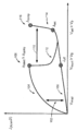
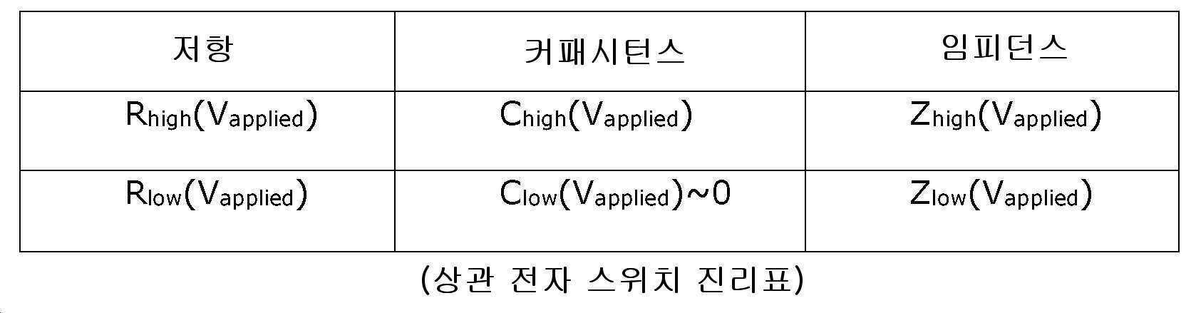
도 1은 상관 전자 스위치(CES) 엘리먼트에 대한 전류 밀도 대 전압의 플롯을 도시한다.
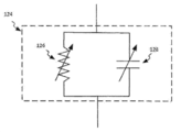
도 2는 CES 장치에 대한 등가 회로의 개략도이다.
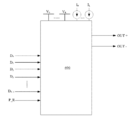
도 3은 설정 가능한 임피더 회로의 예를 개략적으로 도시한다.
도 4는 설정 가능한 임피더의 예시적인 구성을 도시한다.
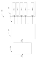
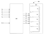
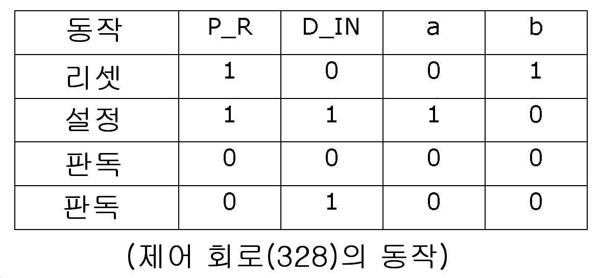
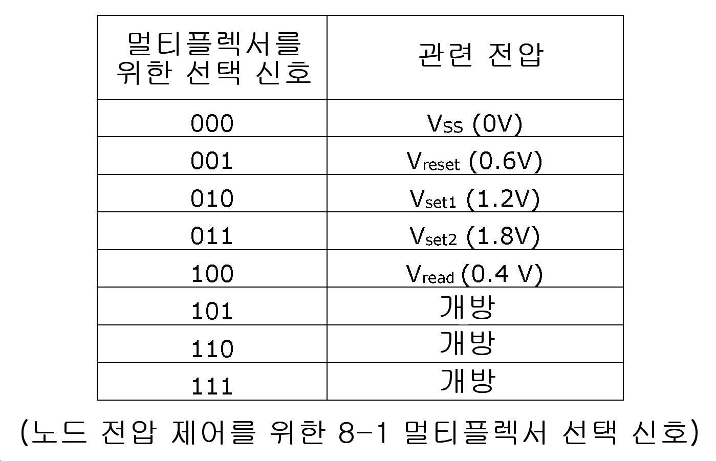
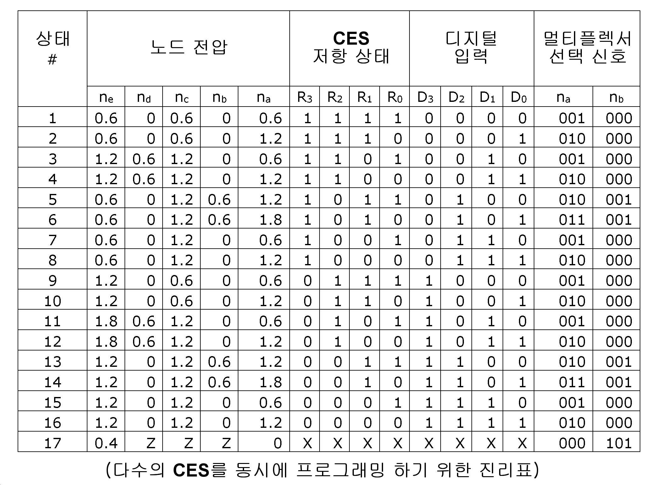
도 5는 복수의 CES를 사용하여 CES를 프로그래밍하기 위한 예시적인 회로를 도시한다.
도 6은 예시적인 OR 게이트 어레이를 도시한다.
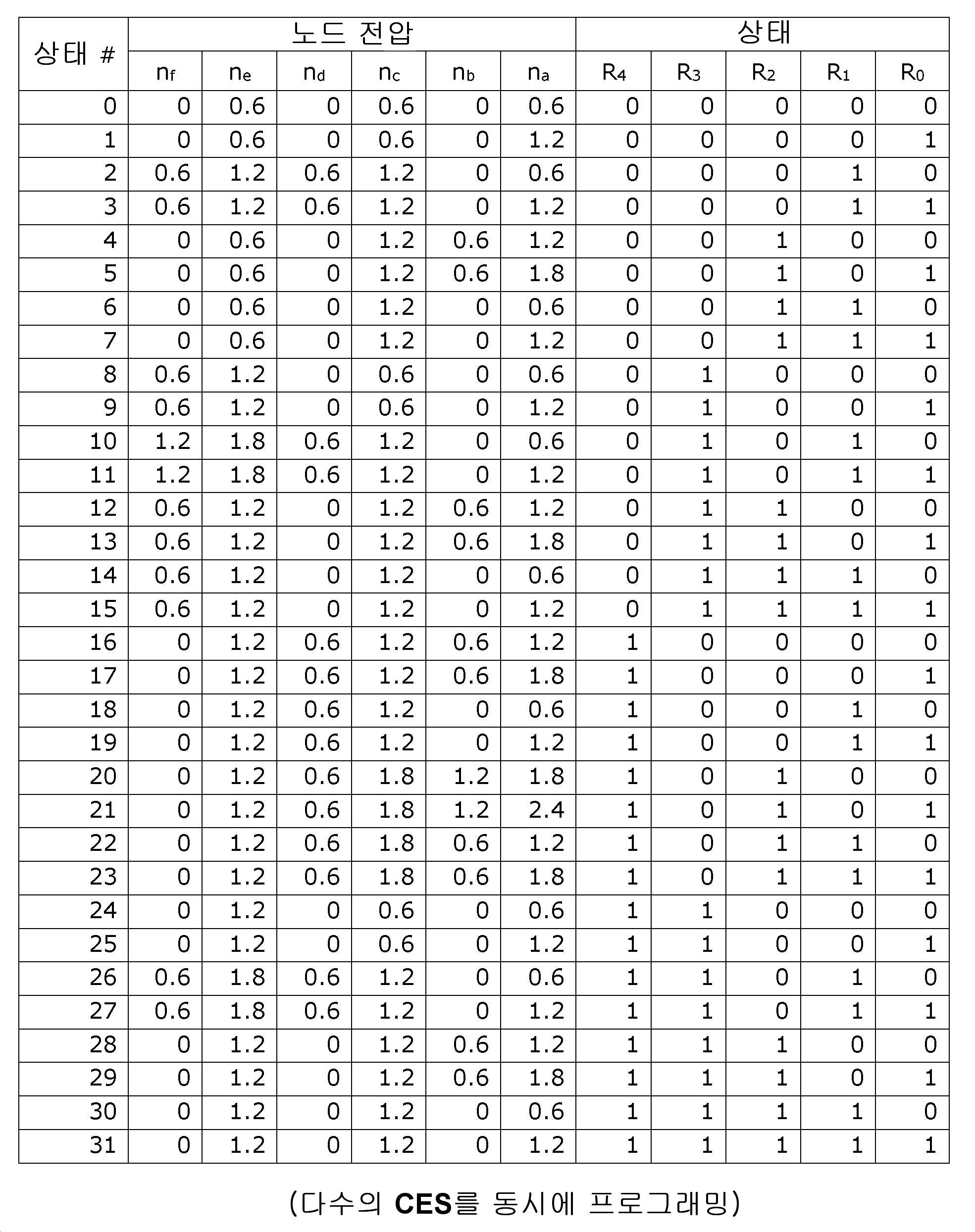
도 7은 다수의 CES를 동시에 프로그래밍하기 위한 예시적인 회로를 도시한다.
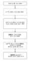
도 8은 설정 가능한 임피더를 제공하기 위한 예시적인 방법을 도시한다.
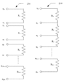
도 9는 예시적인 디지털-아날로그 컨버터(DAC)를 도시한다.
도 10은 하나 이상의 CES 엘리먼트를 포함하는 예시적인 메모리 어레이를 도시한다.
Claims (17)
- 설정 가능한 임피더를 형성하도록 배열된 복수의 상관 전자 스위치(CES)로서, 각각의 CES는 복수의 임피던스 상태 중 하나로 구성될 수 있는 상기 복수의 상관 전자 스위치; 및
적어도 하나의 입력 신호에 각각 따르는 복수의 프로그래밍 신호를 제공하도록 구성된 적어도 하나의 프로그래밍 회로로서, 상기 각각의 프로그래밍 신호는 CES의 임피던스 상태를 구성하는 상기 프로그래밍 회로;
를 포함하는 것을 특징으로 하는 회로. - 제1 항에 있어서, 상기 적어도 하나의 프로그래밍 회로는 복수의 프로그래밍 회로를 포함하고, 각각의 프로그래밍 회로는 상기 복수의 프로그래밍 신호 중 하나를 제공하도록 구성되는 것을 특징으로 하는 회로.
- 제2 항에 있어서, 상기 복수의 임피던스 상태는 제1 임피던스 상태 및 제2 임피던스 상태를 포함하고, 각각의 프로그래밍 회로는:
상기 CES를 상기 제1 임피던스 상태로 구성하기 위한 제1 프로그래밍 신호를 제공하는 제1 구동 회로; 및
상기 CES를 상기 제2 임피던스 상태로 구성하기 위한 제2 프로그래밍 신호를 제공하는 제2 구동 회로;
를 포함하고,
상기 제1 프로그래밍 신호 및 상기 제2 프로그래밍 신호 중 하나는 상기 적어도 하나의 입력 신호에 따르는 것을 특징으로 하는 회로. - 제2 항 또는 제3 항에 있어서, 상기 또는 각각의 프로그래밍 회로에 결합되고, 상기 프로그래밍 회로가 상기 적어도 하나의 입력 신호에 따르는 각각의 프로그래밍 신호를 제공할 수 있도록 배열되는 논리 회로를 더 포함하는 것을 특징으로 하는 회로.
- 제1 항 내지 제4 항 중 어느 한 항에 있어서, 제어 회로를 더 포함하고, 상기 제어 회로는:
상기 적어도 하나의 입력 신호를 수신하고; 및
상기 적어도 하나의 입력 신호에 따라 적어도 하나의 제어 신호를 상기 적어도 하나의 프로그래밍 회로에 제공하도록;
구성되고,
상기 적어도 하나의 프로그래밍 회로는 상기 적어도 하나의 제어 신호에 따르는 상기 복수의 프로그래밍 신호를 제공하는 것을 특징으로 하는 회로. - 제1 항 내지 제5 항 중 어느 한 항에 있어서, 상기 적어도 하나의 프로그래밍 회로는 적어도 하나의 다른 CES의 임피던스 상태가 변하지 않게 유지하면서 하나의 CES의 임피던스 상태가 구성되도록 상기 복수의 프로그래밍 신호를 제공하는 것을 특징으로 하는 회로.
- 제1 항 내지 제6 항 중 어느 한 항에 있어서, 상기 적어도 하나의 프로그래밍 회로는 상기 복수의 CES의 나머지 CES의 임피던스 상태가 변하지 않게 유지하면서 2개 이상의 CES의 임피던스 상태가 구성되도록 상기 복수의 프로그래밍 신호를 제공하는 것을 특징으로 하는 회로.
- 제1 항 내지 제7 항 중 어느 한 항에 있어서, 상기 복수의 임피던스 상태는 적어도 고 임피던스 상태 및 저 임피던스 상태를 포함하는 것을 특징으로 하는 회로.
- 복수의 상관 전자 스위치(CES)를 포함하는 설정 가능한 임피더의 임피던스를 구성하는 방법으로서,
적어도 하나의 입력 신호를 수신하는 단계;
상기 적어도 하나의 입력 신호에 따르는 적어도 하나의 프로그래밍 신호를 판정하는 단계로서, 상기 프로그래밍 신호 또는 상기 각각의 프로그래밍 신호는 상기 복수의 CES 중 하나 이상의 CES의 임피던스 상태를 구성하는 상기 판정하는 단계; 및
상기 CES 또는 각각의 CES의 상기 임피던스 상태를 구성하기 위해 상기 프로그래밍 신호를 상기 복수의 CES 중 하나 이상의 CES에 인가하는 단계;
를 포함하는 것을 특징으로 하는 설정 가능한 임피더의 임피던스를 구성하는 방법. - 제9 항에 있어서, 상기 프로그래밍 신호를 CES에 인가하는 단계는 상기 복수의 CES 중 적어도 하나의 다른 CES의 임피던스 상태를 변경하지 않게 유지하는 단계를 포함하는 것을 특징으로 하는 설정 가능한 임피더의 임피던스를 구성하는 방법
- 제9 항 또는 제10 항에 있어서, 상기 프로그래밍 신호를 CES에 인가하는 단계는 나머지 CES의 상기 임피던스 상태를 변경하지 않게 유지하는 단계를 포함하는 것을 특징으로 하는 설정 가능한 임피더의 임피던스를 구성하는 방법.
- 제9 항 내지 제11 항 중 어느 한 항에 있어서, 상기 프로그래밍 신호를 인가하는 단계는 복수의 임피던스 상태 중 하나의 상태로 CES를 구성하는 단계를 포함하는 것을 특징으로 하는 설정 가능한 임피더의 임피던스를 구성하는 방법.
- 제12 항에 있어서, 상기 복수의 임피던스 상태는 고 임피던스 상태 및 저 임피던스 상태를 포함하는 것을 특징으로 하는 설정 가능한 임피더의 임피던스를 구성하는 방법.
- 디지털-아날로그 컨버터(DAC) 회로에 있어서,
복수의 디지털 입력 신호를 수신하도록 구성된 복수의 데이터 입력;
복수의 상관 전자 스위치(CES) 중 각각의 CES가 상기 복수의 디지털 입력 신호에 따르는 복수의 임피던스 상태 중 하나의 임피던스 상태로 설정 가능한 복수의 CES; 및
적어도 하나의 아날로그 출력 신호를 출력하도록 구성된 적어도 하나의 출력으로서, 상기 아날로그 출력 신호 또는 각각의 아날로그 출력 신호는 상기 복수의 CES의 임피던스 상태들에 따르는 상기 적어도 하나의 출력;
을 포함하는 것을 특징으로 하는 디지털-아날로그 컨버터. - 제14 항에 있어서, 제어 회로를 더 포함하고, 상기 제어 회로는:
기록 신호인 적어도 하나의 입력 신호를 수신하고;
각각의 프로그래밍 신호가 CES의 상기 임피던스 상태를 구성하는, 상기 복수의 디지털 입력 신호에 따라 상기 복수의 CES에 복수의 프로그래밍 신호를 제공하도록;
구성되는 것을 특징으로 하는 디지털-아날로그 컨버터. - 제14 항 또는 제15 항에 있어서, 제어 회로를 더 포함하고, 상기 제어 회로는:
판독 신호인 적어도 하나의 입력 신호를 수신하고; 및
상기 적어도 하나의 아날로그 출력 신호를 출력하기 위해 상기 복수의 CES에 기준 신호를 제공하도록;
구성되는 것을 특징으로 하는 디지털-아날로그 컨버터. - 제14 항, 제15 항, 및 제16 항 중 어느 한 항에 있어서, 상기 복수의 임피던스 상태는 적어도 저 임피던스 상태 및 고 임피던스 상태를 포함하는 것을 특징으로 하는 디지털-아날로그 컨버터.
Applications Claiming Priority (3)
| Application Number | Priority Date | Filing Date | Title |
|---|---|---|---|
| US14/979,156 | 2015-12-22 | ||
| US14/979,156 US9773550B2 (en) | 2015-12-22 | 2015-12-22 | Circuit and method for configurable impedance array |
| PCT/GB2016/053931 WO2017109460A1 (en) | 2015-12-22 | 2016-12-14 | Circuit and method for configurable impedance array |
Publications (2)
| Publication Number | Publication Date |
|---|---|
| KR20180098309A true KR20180098309A (ko) | 2018-09-03 |
| KR102673064B1 KR102673064B1 (ko) | 2024-06-10 |
Family
ID=57737748
Family Applications (1)
| Application Number | Title | Priority Date | Filing Date |
|---|---|---|---|
| KR1020187020703A Active KR102673064B1 (ko) | 2015-12-22 | 2016-12-14 | 설정 가능한 임피던스 어레이를 위한 회로 및 방법 |
Country Status (5)
| Country | Link |
|---|---|
| US (3) | US9773550B2 (ko) |
| KR (1) | KR102673064B1 (ko) |
| CN (1) | CN108604459B (ko) |
| TW (1) | TWI728020B (ko) |
| WO (1) | WO2017109460A1 (ko) |
Cited By (1)
| Publication number | Priority date | Publication date | Assignee | Title |
|---|---|---|---|---|
| KR20220113451A (ko) * | 2020-01-28 | 2022-08-12 | 마이크론 테크놀로지, 인크. | 메모리 디바이스를 이용한 아날로그 저장 |
Families Citing this family (27)
| Publication number | Priority date | Publication date | Assignee | Title |
|---|---|---|---|---|
| US9558819B1 (en) | 2015-08-13 | 2017-01-31 | Arm Ltd. | Method, system and device for non-volatile memory device operation |
| US9755146B2 (en) | 2015-09-10 | 2017-09-05 | ARM, Ltd. | Asymmetric correlated electron switch operation |
| US10797238B2 (en) | 2016-01-26 | 2020-10-06 | Arm Ltd. | Fabricating correlated electron material (CEM) devices |
| US9747982B1 (en) | 2016-02-22 | 2017-08-29 | Arm Ltd. | Device and method for generating random numbers |
| US10276795B2 (en) | 2016-08-15 | 2019-04-30 | Arm Ltd. | Fabrication of correlated electron material film via exposure to ultraviolet energy |
| US10128438B2 (en) | 2016-09-09 | 2018-11-13 | Arm Limited | CEM switching device |
| US10103327B2 (en) | 2016-09-14 | 2018-10-16 | Arm Limited | CEM switching device |
| US9978942B2 (en) | 2016-09-20 | 2018-05-22 | Arm Ltd. | Correlated electron switch structures and applications |
| US10267831B2 (en) * | 2016-09-30 | 2019-04-23 | Arm Ltd. | Process variation compensation with correlated electron switch devices |
| US9997242B2 (en) | 2016-10-14 | 2018-06-12 | Arm Ltd. | Method, system and device for non-volatile memory device state detection |
| US9899083B1 (en) | 2016-11-01 | 2018-02-20 | Arm Ltd. | Method, system and device for non-volatile memory device operation with low power high speed and high density |
| US10121967B2 (en) * | 2016-11-29 | 2018-11-06 | Arm Limited | CEM switching device |
| US9871528B1 (en) * | 2016-11-30 | 2018-01-16 | Arm Ltd. | Digital to analog conversion with correlated electron switch devices |
| US10002669B1 (en) | 2017-05-10 | 2018-06-19 | Arm Ltd. | Method, system and device for correlated electron switch (CES) device operation |
| US10211398B2 (en) | 2017-07-03 | 2019-02-19 | Arm Ltd. | Method for the manufacture of a correlated electron material device |
| GB2567215B (en) * | 2017-10-06 | 2020-04-01 | Advanced Risc Mach Ltd | Reconfigurable circuit architecture |
| US10714175B2 (en) | 2017-10-10 | 2020-07-14 | ARM, Ltd. | Method, system and device for testing correlated electron switch (CES) devices |
| US10229731B1 (en) | 2017-10-11 | 2019-03-12 | Arm Ltd. | Method, system and circuit for staggered boost injection |
| US11137919B2 (en) | 2017-10-30 | 2021-10-05 | Arm Ltd. | Initialisation of a storage device |
| US11636316B2 (en) | 2018-01-31 | 2023-04-25 | Cerfe Labs, Inc. | Correlated electron switch elements for brain-based computing |
| US10224099B1 (en) | 2018-02-06 | 2019-03-05 | Arm Ltd. | Method, system and device for error correction in reading memory devices |
| US10741246B2 (en) | 2018-04-23 | 2020-08-11 | Arm Limited | Method, system and device for integration of volatile and non-volatile memory bitcells |
| US10607659B2 (en) | 2018-04-23 | 2020-03-31 | Arm Limited | Method, system and device for integration of bitcells in a volatile memory array and bitcells in a non-volatile memory array |
| US10971229B2 (en) | 2018-04-23 | 2021-04-06 | Arm Limited | Method, system and device for integration of volatile and non-volatile memory bitcells |
| US10580489B2 (en) | 2018-04-23 | 2020-03-03 | Arm Ltd. | Method, system and device for complementary impedance states in memory bitcells |
| US11011227B2 (en) | 2018-06-15 | 2021-05-18 | Arm Ltd. | Method, system and device for non-volatile memory device operation |
| EP4345823A1 (en) * | 2022-09-30 | 2024-04-03 | IHP GmbH - Innovations for High Performance Microelectronics / Leibniz-Institut für innovative Mikroelektronik | Resistive memory subcell, resistive random access memory for in-memory-computing and in-memory-processor |
Citations (2)
| Publication number | Priority date | Publication date | Assignee | Title |
|---|---|---|---|---|
| KR20090078370A (ko) * | 2006-11-08 | 2009-07-17 | 시메트릭스 주식회사 | 저항 스위칭 집적 회로 메모리, 저항 스위칭 메모리의 형성 방법, 저항 스위칭 박막 메모리 구성요소로의 기록 방법 및 비휘발성 저항 스위칭 집적 회로 메모리의 제조 방법 |
| WO2015163928A1 (en) * | 2014-04-26 | 2015-10-29 | Hewlett-Packard Development Company, L.P. | Switched memristor analog-to-digital conversion |
Family Cites Families (25)
| Publication number | Priority date | Publication date | Assignee | Title |
|---|---|---|---|---|
| KR100527559B1 (ko) * | 2004-02-05 | 2005-11-09 | 주식회사 하이닉스반도체 | 직렬 다이오드 셀을 이용한 불휘발성 메모리 장치 |
| US7298640B2 (en) | 2004-05-03 | 2007-11-20 | Symetrix Corporation | 1T1R resistive memory array with chained structure |
| US7443711B1 (en) * | 2004-12-16 | 2008-10-28 | Hewlett-Packard Development Company, L.P. | Non-volatile programmable impedance nanoscale devices |
| US7405462B2 (en) * | 2006-01-31 | 2008-07-29 | Hewlett-Packard Development Company, L.P. | FPGA architecture at conventional and submicron scales |
| US7902867B2 (en) * | 2006-04-03 | 2011-03-08 | Blaise Laurent Mouttet | Memristor crossbar neural interface |
| US7872900B2 (en) * | 2006-11-08 | 2011-01-18 | Symetrix Corporation | Correlated electron memory |
| US20080107801A1 (en) | 2006-11-08 | 2008-05-08 | Symetrix Corporation | Method of making a variable resistance memory |
| US7778063B2 (en) | 2006-11-08 | 2010-08-17 | Symetrix Corporation | Non-volatile resistance switching memories and methods of making same |
| US7639523B2 (en) | 2006-11-08 | 2009-12-29 | Symetrix Corporation | Stabilized resistive switching memory |
| JP5224241B2 (ja) * | 2007-11-06 | 2013-07-03 | Nltテクノロジー株式会社 | 双方向シフトレジスタ、それを用いた表示装置 |
| US7652501B2 (en) * | 2008-01-07 | 2010-01-26 | Unity Semiconductor Corporation | Programmable logic device structure using third dimensional memory |
| WO2009140305A1 (en) * | 2008-05-12 | 2009-11-19 | Symetrix Corporation | Correlated electron material and process for making |
| US20100226163A1 (en) | 2009-03-04 | 2010-09-09 | Savransky Semyon D | Method of resistive memory programming and associated devices and materials |
| KR20120059023A (ko) | 2010-11-30 | 2012-06-08 | 삼성전자주식회사 | 저항 소자 및 이를 이용한 디지털-아날로그 컨버터 |
| US8779407B2 (en) | 2012-02-07 | 2014-07-15 | Intermolecular, Inc. | Multifunctional electrode |
| US8686386B2 (en) | 2012-02-17 | 2014-04-01 | Sandisk 3D Llc | Nonvolatile memory device using a varistor as a current limiter element |
| US8816719B2 (en) | 2012-04-26 | 2014-08-26 | Symetrix Corporation | Re-programmable antifuse FPGA utilizing resistive CeRAM elements |
| US9735766B2 (en) | 2015-07-31 | 2017-08-15 | Arm Ltd. | Correlated electron switch |
| US9851738B2 (en) | 2015-08-13 | 2017-12-26 | Arm Ltd. | Programmable voltage reference |
| US9558819B1 (en) | 2015-08-13 | 2017-01-31 | Arm Ltd. | Method, system and device for non-volatile memory device operation |
| US9748943B2 (en) | 2015-08-13 | 2017-08-29 | Arm Ltd. | Programmable current for correlated electron switch |
| US10096361B2 (en) | 2015-08-13 | 2018-10-09 | Arm Ltd. | Method, system and device for non-volatile memory device operation |
| US9584118B1 (en) | 2015-08-26 | 2017-02-28 | Nxp Usa, Inc. | Substrate bias circuit and method for biasing a substrate |
| US10056143B2 (en) | 2015-09-08 | 2018-08-21 | Arm Ltd. | Correlated electron switch programmable fabric |
| US9589636B1 (en) | 2015-09-22 | 2017-03-07 | Arm Ltd. | Method, system and device for complementary non-volatile memory device operation |
-
2015
- 2015-12-22 US US14/979,156 patent/US9773550B2/en active Active
-
2016
- 2016-12-14 KR KR1020187020703A patent/KR102673064B1/ko active Active
- 2016-12-14 CN CN201680075565.3A patent/CN108604459B/zh active Active
- 2016-12-14 WO PCT/GB2016/053931 patent/WO2017109460A1/en not_active Ceased
- 2016-12-22 TW TW105142665A patent/TWI728020B/zh active
-
2017
- 2017-03-08 US US15/453,721 patent/US9905295B2/en active Active
-
2018
- 2018-01-08 US US15/865,116 patent/US10381076B2/en active Active
Patent Citations (2)
| Publication number | Priority date | Publication date | Assignee | Title |
|---|---|---|---|---|
| KR20090078370A (ko) * | 2006-11-08 | 2009-07-17 | 시메트릭스 주식회사 | 저항 스위칭 집적 회로 메모리, 저항 스위칭 메모리의 형성 방법, 저항 스위칭 박막 메모리 구성요소로의 기록 방법 및 비휘발성 저항 스위칭 집적 회로 메모리의 제조 방법 |
| WO2015163928A1 (en) * | 2014-04-26 | 2015-10-29 | Hewlett-Packard Development Company, L.P. | Switched memristor analog-to-digital conversion |
Cited By (1)
| Publication number | Priority date | Publication date | Assignee | Title |
|---|---|---|---|---|
| KR20220113451A (ko) * | 2020-01-28 | 2022-08-12 | 마이크론 테크놀로지, 인크. | 메모리 디바이스를 이용한 아날로그 저장 |
Also Published As
| Publication number | Publication date |
|---|---|
| US20180218772A1 (en) | 2018-08-02 |
| WO2017109460A1 (en) | 2017-06-29 |
| CN108604459A (zh) | 2018-09-28 |
| US9773550B2 (en) | 2017-09-26 |
| US20170178724A1 (en) | 2017-06-22 |
| CN108604459B (zh) | 2022-07-01 |
| US20170206963A1 (en) | 2017-07-20 |
| US9905295B2 (en) | 2018-02-27 |
| US10381076B2 (en) | 2019-08-13 |
| TWI728020B (zh) | 2021-05-21 |
| TW201801082A (zh) | 2018-01-01 |
| KR102673064B1 (ko) | 2024-06-10 |
Similar Documents
| Publication | Publication Date | Title |
|---|---|---|
| KR102673064B1 (ko) | 설정 가능한 임피던스 어레이를 위한 회로 및 방법 | |
| CN108028065B (zh) | 用于互补非易失性存储器设备操作的方法、系统和设备 | |
| US11355192B2 (en) | CES-based latching circuits | |
| CN108475527B (zh) | 锁存设备和方法 | |
| TWI772269B (zh) | 用於相關電子開關的方法及設備 | |
| KR101711109B1 (ko) | 더미 저항, 저항 스위칭 소자들 및 다이오드들을 포함하는 다중비트 저항-스위칭 메모리 셀을 기록하는 방법 | |
| US8619457B2 (en) | Three-device non-volatile memory cell | |
| CN110383301A (zh) | 尖峰神经网络 | |
| KR101600969B1 (ko) | 다이오드를 갖는 교차점 비휘발성 메모리 셀의 기록 방법 | |
| KR20180063122A (ko) | 상관 전자 스위치 프로그래밍 가능한 구조 | |
| KR20180125580A (ko) | 논리 회로 사이의 접속 소자로서의 상관 전자 저항성 메모리 소자 | |
| CN111771214A (zh) | 用于基于脑的计算的相关电子开关元件 | |
| US10777273B2 (en) | Cross-point storage array including correlated electron switches | |
| CN109891505B (zh) | 存储元件中的选择性写入 | |
| US11061852B2 (en) | Reconfigurable circuit architecture |
Legal Events
| Date | Code | Title | Description |
|---|---|---|---|
| PA0105 | International application |
Patent event date: 20180718 Patent event code: PA01051R01D Comment text: International Patent Application |
|
| PG1501 | Laying open of application | ||
| A201 | Request for examination | ||
| PA0201 | Request for examination |
Patent event code: PA02012R01D Patent event date: 20211116 Comment text: Request for Examination of Application |
|
| E902 | Notification of reason for refusal | ||
| PE0902 | Notice of grounds for rejection |
Comment text: Notification of reason for refusal Patent event date: 20230726 Patent event code: PE09021S01D |
|
| AMND | Amendment | ||
| E601 | Decision to refuse application | ||
| PE0601 | Decision on rejection of patent |
Patent event date: 20231102 Comment text: Decision to Refuse Application Patent event code: PE06012S01D Patent event date: 20230726 Comment text: Notification of reason for refusal Patent event code: PE06011S01I |
|
| X091 | Application refused [patent] | ||
| AMND | Amendment | ||
| PX0901 | Re-examination |
Patent event code: PX09011S01I Patent event date: 20231102 Comment text: Decision to Refuse Application Patent event code: PX09012R01I Patent event date: 20230914 Comment text: Amendment to Specification, etc. |
|
| PX0701 | Decision of registration after re-examination |
Patent event date: 20240426 Comment text: Decision to Grant Registration Patent event code: PX07013S01D Patent event date: 20240319 Comment text: Amendment to Specification, etc. Patent event code: PX07012R01I Patent event date: 20231102 Comment text: Decision to Refuse Application Patent event code: PX07011S01I Patent event date: 20230914 Comment text: Amendment to Specification, etc. Patent event code: PX07012R01I |
|
| X701 | Decision to grant (after re-examination) | ||
| GRNT | Written decision to grant | ||
| PR0701 | Registration of establishment |
Comment text: Registration of Establishment Patent event date: 20240603 Patent event code: PR07011E01D |
|
| PR1002 | Payment of registration fee |
Payment date: 20240604 End annual number: 3 Start annual number: 1 |
|
| PG1601 | Publication of registration |