KR20180098309A - Circuits and Methods for a Configurable Impedance Array - Google Patents
Circuits and Methods for a Configurable Impedance Array Download PDFInfo
- Publication number
- KR20180098309A KR20180098309A KR1020187020703A KR20187020703A KR20180098309A KR 20180098309 A KR20180098309 A KR 20180098309A KR 1020187020703 A KR1020187020703 A KR 1020187020703A KR 20187020703 A KR20187020703 A KR 20187020703A KR 20180098309 A KR20180098309 A KR 20180098309A
- Authority
- KR
- South Korea
- Prior art keywords
- programming
- ces
- signal
- impedance
- circuit
- Prior art date
- Legal status (The legal status is an assumption and is not a legal conclusion. Google has not performed a legal analysis and makes no representation as to the accuracy of the status listed.)
- Granted
Links
Images


Classifications
-
- G—PHYSICS
- G11—INFORMATION STORAGE
- G11C—STATIC STORES
- G11C13/00—Digital stores characterised by the use of storage elements not covered by groups G11C11/00, G11C23/00, or G11C25/00
- G11C13/0002—Digital stores characterised by the use of storage elements not covered by groups G11C11/00, G11C23/00, or G11C25/00 using resistive RAM [RRAM] elements
- G11C13/0021—Auxiliary circuits
- G11C13/0069—Writing or programming circuits or methods
-
- G—PHYSICS
- G11—INFORMATION STORAGE
- G11C—STATIC STORES
- G11C11/00—Digital stores characterised by the use of particular electric or magnetic storage elements; Storage elements therefor
- G11C11/21—Digital stores characterised by the use of particular electric or magnetic storage elements; Storage elements therefor using electric elements
- G11C11/34—Digital stores characterised by the use of particular electric or magnetic storage elements; Storage elements therefor using electric elements using semiconductor devices
- G11C11/36—Digital stores characterised by the use of particular electric or magnetic storage elements; Storage elements therefor using electric elements using semiconductor devices using diodes, e.g. as threshold elements, i.e. diodes assuming a stable ON-stage when driven above their threshold (S- or N-characteristic)
- G11C11/38—Digital stores characterised by the use of particular electric or magnetic storage elements; Storage elements therefor using electric elements using semiconductor devices using diodes, e.g. as threshold elements, i.e. diodes assuming a stable ON-stage when driven above their threshold (S- or N-characteristic) using tunnel diodes
-
- G—PHYSICS
- G11—INFORMATION STORAGE
- G11C—STATIC STORES
- G11C13/00—Digital stores characterised by the use of storage elements not covered by groups G11C11/00, G11C23/00, or G11C25/00
- G11C13/0002—Digital stores characterised by the use of storage elements not covered by groups G11C11/00, G11C23/00, or G11C25/00 using resistive RAM [RRAM] elements
- G11C13/0004—Digital stores characterised by the use of storage elements not covered by groups G11C11/00, G11C23/00, or G11C25/00 using resistive RAM [RRAM] elements comprising amorphous/crystalline phase transition cells
-
- G—PHYSICS
- G11—INFORMATION STORAGE
- G11C—STATIC STORES
- G11C13/00—Digital stores characterised by the use of storage elements not covered by groups G11C11/00, G11C23/00, or G11C25/00
- G11C13/0002—Digital stores characterised by the use of storage elements not covered by groups G11C11/00, G11C23/00, or G11C25/00 using resistive RAM [RRAM] elements
- G11C13/0021—Auxiliary circuits
- G11C13/003—Cell access
-
- G—PHYSICS
- G11—INFORMATION STORAGE
- G11C—STATIC STORES
- G11C13/00—Digital stores characterised by the use of storage elements not covered by groups G11C11/00, G11C23/00, or G11C25/00
- G11C13/0002—Digital stores characterised by the use of storage elements not covered by groups G11C11/00, G11C23/00, or G11C25/00 using resistive RAM [RRAM] elements
- G11C13/0021—Auxiliary circuits
- G11C13/004—Reading or sensing circuits or methods
-
- G—PHYSICS
- G11—INFORMATION STORAGE
- G11C—STATIC STORES
- G11C17/00—Read-only memories programmable only once; Semi-permanent stores, e.g. manually-replaceable information cards
- G11C17/08—Read-only memories programmable only once; Semi-permanent stores, e.g. manually-replaceable information cards using semiconductor devices, e.g. bipolar elements
- G11C17/10—Read-only memories programmable only once; Semi-permanent stores, e.g. manually-replaceable information cards using semiconductor devices, e.g. bipolar elements in which contents are determined during manufacturing by a predetermined arrangement of coupling elements, e.g. mask-programmable ROM
- G11C17/12—Read-only memories programmable only once; Semi-permanent stores, e.g. manually-replaceable information cards using semiconductor devices, e.g. bipolar elements in which contents are determined during manufacturing by a predetermined arrangement of coupling elements, e.g. mask-programmable ROM using field-effect devices
-
- H—ELECTRICITY
- H03—ELECTRONIC CIRCUITRY
- H03M—CODING; DECODING; CODE CONVERSION IN GENERAL
- H03M1/00—Analogue/digital conversion; Digital/analogue conversion
- H03M1/66—Digital/analogue converters
- H03M1/74—Simultaneous conversion
- H03M1/78—Simultaneous conversion using ladder network
-
- H—ELECTRICITY
- H03—ELECTRONIC CIRCUITRY
- H03M—CODING; DECODING; CODE CONVERSION IN GENERAL
- H03M1/00—Analogue/digital conversion; Digital/analogue conversion
- H03M1/66—Digital/analogue converters
- H03M1/74—Simultaneous conversion
- H03M1/80—Simultaneous conversion using weighted impedances
- H03M1/808—Simultaneous conversion using weighted impedances using resistors
-
- G—PHYSICS
- G11—INFORMATION STORAGE
- G11C—STATIC STORES
- G11C2213/00—Indexing scheme relating to G11C13/00 for features not covered by this group
- G11C2213/70—Resistive array aspects
- G11C2213/75—Array having a NAND structure comprising, for example, memory cells in series or memory elements in series, a memory element being a memory cell in parallel with an access transistor
-
- H—ELECTRICITY
- H03—ELECTRONIC CIRCUITRY
- H03M—CODING; DECODING; CODE CONVERSION IN GENERAL
- H03M1/00—Analogue/digital conversion; Digital/analogue conversion
Landscapes
- Logic Circuits (AREA)
- Engineering & Computer Science (AREA)
- Theoretical Computer Science (AREA)
- Semiconductor Memories (AREA)
- Computer Hardware Design (AREA)
- Chemical & Material Sciences (AREA)
- Crystallography & Structural Chemistry (AREA)
- Design And Manufacture Of Integrated Circuits (AREA)
Abstract
설정 가능한 임피더가 제공된다. 설정 가능한 임피더는 다수의 상관 전자 스위치(CES)를 포함한다. 각 CES는 복수의 임피던스 상태 중 하나로 구성될 수 있다. 또한, 프로그래밍 회로가 제공된다. 프로그래밍 회로는 입력 신호에 따라 복수의 프로그래밍 신호를 제공한다. 각각의 프로그래밍 신호는 복수의 CES로부터 각각의 CES의 임피던스 상태를 구성한다.A configurable impedance is provided. The configurable impedance includes a plurality of correlated electronic switches (CES). Each CES can be configured with one of a plurality of impedance states. In addition, a programming circuit is provided. The programming circuit provides a plurality of programming signals according to an input signal. Each programming signal constitutes the impedance state of each CES from a plurality of CESs.
Description
본 기술은 일반적으로 설정 가능한 임피더에 관한 것으로, 특히, 적어도 하나의 상관 전자 스위치(CES)로 구성된 설정 가능한 임피더에 관한 것이다.The technique relates generally to configurable impedance, and more particularly to a configurable impedance configured with at least one correlated electronic switch (CES).
레지스터 체인과 같은 프로그램 가능 임피더는 디지털 아날로그 컨버터의 저항 래더 및 신경 회로망의 저항 어레이와 같은 다수의 아날로그 신호 처리 애플리케이션에 활용할 수 있다. 레지스터 체인을 프로그래밍하기 위한 다양한 기술이 제공되었다. 그러나, 프로그래밍 전압 및 전류의 불확실성은 그러한 프로그래밍 기술에서 흔히 발생한다.Programmable imagers, such as resistor chains, can be utilized in a number of analog signal processing applications, such as resistor ladders in digital-to-analog converters and resistive arrays in neural networks. Various techniques for programming register chains have been provided. However, the uncertainty of programming voltage and current is common in such programming techniques.
본 발명에 따르면, 적어도 하나의 상관 전자 스위치(CES)로 구성된 설정 가능한 임피더를 제공할 수 있다.According to the present invention, it is possible to provide a configurable impedance configured with at least one correlated electronic switch (CES).
본 기술의 제1 양태에 따르면, 설정 가능한 임피더를 형성하도록 배치된 복수의 상관 전자 스위치(CES)로서, 각각의 CES는 복수의 임피던스 상태 중 하나로 구성될 수 있는 상기 복수의 상관 전자 스위치; 및 각각 적어도 하나의 입력 신호에 따르는 복수의 프로그래밍 신호를 제공하도록 구성된 적어도 하나의 프로그래밍 회로로서, 각각의 프로그래밍 신호는 CES의 임피던스 상태를 구성하는 상기 프로그래밍 회로;를 포함하는 회로가 제공된다.According to a first aspect of the present technology, there is provided a plurality of correlated electronic switches (CES) arranged to form a configurable impedance, wherein each CES can be configured in one of a plurality of impedance states; And at least one programming circuit configured to provide a plurality of programming signals each corresponding to at least one input signal, wherein each programming signal constitutes an impedance state of the CES.
실시 예에서, 상기 적어도 하나의 프로그래밍 회로는 복수의 프로그래밍 회로를 포함하고, 각각의 프로그래밍 회로는 복수의 프로그래밍 신호 중 하나를 제공하도록 구성된다.In an embodiment, the at least one programming circuit includes a plurality of programming circuits, and each programming circuit is configured to provide one of a plurality of programming signals.
상기 복수의 임피던스 상태는 제1 임피던스 상태 및 제2 임피던스 상태를 포함할 수 있다. 실시 예에서, 각각의 프로그래밍 회로는: 상기 CES를 상기 제1 임피던스 상태로 구성하기 위해 제1 프로그래밍 신호를 제공하는 제1 구동 회로; 및 상기 CES를 상기 제2 임피던스 상태로 구성하기 위해 제2 프로그래밍 신호를 제공하는 제2 구동 회로;를 포함하고, 상기 제1 프로그래밍 신호 및 상기 제2 프로그래밍 신호 중 하나는 상기 적어도 하나의 입력 신호에 따른다.The plurality of impedance states may include a first impedance state and a second impedance state. In an embodiment, each programming circuit includes: a first driving circuit for providing a first programming signal to configure the CES to the first impedance state; And a second driving circuit for providing a second programming signal to configure the CES to the second impedance state, wherein one of the first programming signal and the second programming signal is applied to the at least one input signal Follow.
상기 회로는 상기 또는 각각의 프로그래밍 회로에 결합되고 상기 프로그래밍 회로가 상기 적어도 하나의 입력 신호에 따른 각각의 프로그래밍 신호를 제공할 수 있도록 배열된 논리 회로를 더 포함할 수 있다.The circuit may further comprise a logic circuit coupled to the or each programming circuit and the programming circuit being arranged to provide a respective programming signal according to the at least one input signal.
상기 회로는, 상기 적어도 하나의 입력 신호를 수신하고; 상기 적어도 하나의 입력 신호에 따라 적어도 하나의 제어 신호를 상기 적어도 하나의 프로그래밍 회로에 제공하도록; 구성되는 제어 회로를 더 포함하고, 상기 적어도 하나의 프로그래밍 회로는 상기 적어도 하나의 제어 신호에 따르는 상기 복수의 프로그래밍 신호를 제공한다.The circuitry comprising: receiving the at least one input signal; Provide at least one control signal to the at least one programming circuit in accordance with the at least one input signal; Wherein the at least one programming circuit provides the plurality of programming signals according to the at least one control signal.
실시 예에서, 적어도 하나의 프로그래밍 회로는 적어도 하나의 다른 CES의 임피던스 상태를 변경하지 않게 유지하면서 하나의 CES의 임피던스 상태가 구성되도록 상기 복수의 프로그래밍 신호를 제공한다. 부가적으로 또는 대안으로, 상기 적어도 하나의 프로그래밍 회로는 상기 복수의 CES의 나머지 CES의 임피던스 상태를 변경하지 않게 유지하면서 2개 이상의 CES의 임피던스 상태가 구성되도록 상기 복수의 프로그래밍 신호를 제공한다.In an embodiment, at least one programming circuit provides the plurality of programming signals such that the impedance state of one CES is configured while maintaining the impedance state of at least one other CES unchanged. Additionally or alternatively, the at least one programming circuit provides the plurality of programming signals such that impedance states of two or more CESs are configured while maintaining the impedance state of the remaining CESs of the plurality of CESs unchanged.
상기 복수의 임피던스 상태는 (적어도) 고 임피던스 상태 및 저 임피던스 상태를 포함할 수 있다.The plurality of impedance states may include (at least) a high impedance state and a low impedance state.
본 기술의 제2 양태에서, 복수의 상관 전자 스위치(CES)를 포함하는 설정 가능한 임피더의 임피던스를 구성하는 방법이 제공되며, 상기 방법은: 적어도 하나의 입력 신호를 수신하는 단계; 상기 적어도 하나의 입력 신호에 따르는 적어도 하나의 프로그래밍 신호를 판정하는 단계로서, 상기 프로그래밍 신호 또는 상기 각각의 프로그래밍 신호는 상기 복수의 CES 중 하나 이상의 CES의 임피던스 상태를 구성 하는 상기 판정하는 단계; 및 상기 CES 또는 각각의 CES의 상기 임피던스 상태를 구성하기 위해 상기 프로그래밍 신호를 상기 복수의 CES 중 하나 이상의 CES에 인가하는 단계;를 포함한다.In a second aspect of the present technique, a method is provided for configuring an impedance of a configurable impedance, comprising a plurality of correlated electronic switches (CES), the method comprising: receiving at least one input signal; Determining at least one programming signal that follows the at least one input signal, wherein the programming signal or each programming signal comprises an impedance state of at least one of the plurality of CESs; And applying the programming signal to one or more of the plurality of CESs to configure the impedance state of the CES or each CES.
상기 프로그래밍 신호를 CES에 인가하는 단계는 상기 복수의 CES 중 적어도 하나의 다른 CES의 임피던스 상태를 변경하지 않게 유지하는 단계를 포함할 수 있다. 부가적으로 또는 대안으로, 상기 프로그래밍 신호를 CES에 인가하는 단계는 나머지 CES의 임피던스 상태를 변경하지 않게 유지하는 단계를 포함할 수 있다.The step of applying the programming signal to the CES may include maintaining the impedance state of at least one other CES among the plurality of CESs unchanged. Additionally or alternatively, applying the programming signal to the CES may include maintaining the impedance state of the remaining CES unchanged.
실시 예에서, 상기 프로그래밍 신호를 인가하는 단계는 복수의 임피던스 상태 중 하나로 CES를 구성하는 단계를 포함한다. 상기 복수의 임피던스 상태는 고 임피던스 상태 및 저 임피던스 상태를 포함할 수 있다.In an embodiment, applying the programming signal comprises configuring a CES with one of a plurality of impedance states. The plurality of impedance states may include a high impedance state and a low impedance state.
본 기술의 제3 양태에서, 복수의 디지털 입력 신호를 수신하도록 구성된 복수의 데이터 입력; 각각의 상관 전자 스위치(CES)가 상기 복수의 디지털 입력 신호에 따르는 복수의 임피던스 상태 중 하나의 임피던스 상태로 설정 가능한 상기 복수의 CES; 및 적어도 하나의 아날로그 출력 신호를 출력하도록 구성된 적어도 하나의 출력으로서, 상기 아날로그 출력 신호 또는 각각의 아날로그 출력 신호는 상기 복수의 CES의 임피던스 상태에 따르는 상기 적어도 하나의 출력;을 포함하는 디지털-아날로그 컨버터(DAC)가 제공된다.In a third aspect of the technique, a plurality of data inputs configured to receive a plurality of digital input signals; Each of said correlating electronic switches (CES) being capable of being set to one of a plurality of impedance states corresponding to said plurality of digital input signals; And at least one output configured to output at least one analog output signal, wherein the analog output signal or each analog output signal corresponds to an impedance state of the plurality of CESs, (DAC) is provided.
상기 DAC는: 기록 신호인 적어도 하나의 입력 신호를 수신하고; 각각의 프로그래밍 신호가 CES의 상기 임피던스 상태를 구성하는, 상기 복수의 디지털 입력 신호에 따르는 상기 복수의 CES에 복수의 프로그래밍 신호를 제공하도록; 구성되는 제어 회로를 포함할 수 있다.The DAC comprising: at least one input signal which is a recording signal; Providing a plurality of programming signals to the plurality of CESs compliant with the plurality of digital input signals, wherein each programming signal constitutes the impedance state of the CES; And may include a control circuit configured.
상기 DAC는: 판독 신호인 적어도 하나의 입력 신호를 수신하고; 상기 적어도 하나의 아날로그 출력 신호를 출력하기 위해 상기 복수의 CES에 기준 신호를 제공하도록; 구성되는 제어 회로를 포함할 수 있다.The DAC comprising: at least one input signal which is a read signal; Providing a reference signal to the plurality of CESs to output the at least one analog output signal; And may include a control circuit configured.
상기 복수의 임피던스 상태는 적어도 저 임피던스 상태 및 고 임피던스 상태를 포함한다.The plurality of impedance states include at least a low-impedance state and a high-impedance state.
상기 기술들은 첨부 도면들에 예시적으로 도식적으로 도시되어 있다:
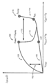
도 1은 상관 전자 스위치(CES) 엘리먼트에 대한 전류 밀도 대 전압의 플롯을 도시한다.
도 2는 CES 장치에 대한 등가 회로의 개략도이다.
도 3은 설정 가능한 임피더 회로의 예를 개략적으로 도시한다.
도 4는 설정 가능한 임피더의 예시적인 구성을 도시한다.
도 5는 복수의 CES를 사용하여 CES를 프로그래밍하기 위한 예시적인 회로를 도시한다.
도 6은 예시적인 OR 게이트 어레이를 도시한다.
도 7은 다수의 CES를 동시에 프로그래밍하기 위한 예시적인 회로를 도시한다.
도 8은 설정 가능한 임피더를 제공하기 위한 예시적인 방법을 도시한다.
도 9는 예시적인 디지털-아날로그 컨버터(DAC)를 도시한다.
도 10은 하나 이상의 CES 엘리먼트를 포함하는 예시적인 메모리 어레이를 도시한다.The techniques are illustrated schematically in the accompanying drawings by way of example:
Figure 1 shows a plot of current density versus voltage for a correlated electronic switch (CES) element.
2 is a schematic diagram of an equivalent circuit for a CES device.
Figure 3 schematically shows an example of a settable impedance circuit.
Figure 4 shows an exemplary configuration of a configurable impoder.
5 illustrates an exemplary circuit for programming a CES using a plurality of CESs.
Figure 6 illustrates an exemplary OR gate array.
Figure 7 illustrates an exemplary circuit for simultaneously programming multiple CESs.
Figure 8 illustrates an exemplary method for providing a configurable impedance.
Figure 9 shows an exemplary digital-to-analog converter (DAC).
10 illustrates an exemplary memory array including one or more CES elements.
광범위하게 말하면, 본 기술의 실시 예는 상관 전자 재료(CEM)를 포함하는 상관 전자 스위치(CES) 엘리먼트를 제공할 수 있다. CES는 회로 내에서 연결을 가능하게 하는 회로 소자뿐만 아니라 비휘발성 저장소로서 모두 사용될 수 있다. 아래에서 더 상세히 설명하는 바와 같이, CES 엘리먼트는 도전성 상태와 절연성 상태 사이에서 재료(적어도 일부분)의 트랜지션에 적어도 부분적으로 기초하여 미리 결정된 검출 가능한 메모리 상태들 사이에서 트랜지션할 수 있는 재료를 포함한다. CES 엘리먼트는 구성을 비휘발성 방식으로 저장하고 자신의 임피던스 상태를 사용하여 연결을 가능하게 할 수 있도록 프로그래밍할 수 있다.Broadly speaking, embodiments of the present technology may provide a correlated electronic switch (CES) element comprising a correlated electronic material (CEM). The CES can be used both as a non-volatile storage as well as a circuit element to enable a connection in a circuit. As described in more detail below, the CES element includes a material capable of transitioning between predetermined detectable memory states based, at least in part, on a transition of a material (at least a portion) between a conductive state and an insulating state. The CES element can be programmed to store the configuration in a nonvolatile manner and enable its connection using its own impedance state.
"상관 전자 스위치"라는 용어는 본 명세서에서 "CES", "CES 엘리먼트", "CES 장치", "상관 전자 랜덤 액세스 메모리", "CeRAM"및 "CeRAM 장치"와 교환 가능하게 사용된다.The term "correlated electronic switch" is used interchangeably with "CES", "CES element", "CES device", "correlated electronic random access memory", "CeRAM", and "CeRAM device" herein.
비휘발성 메모리는 메모리 셀 또는 엘리먼트가 장치에 공급된 전력이 제거된 후에 자신의 상태를 잃지 않는 클래스의 메모리이다. 플래시 메모리 장치에서, 속도와 비트 밀도를 높이기 위해 랜덤 액세스(소거/기록 단일 비트) 유지 기능을 희생했다. 플래시는 여전히 비휘발성 메모리의 선택을 유지한다. 그럼에도 불구하고 일반적으로 플래시 메모리 기술은 40 나노 미터(nm) 이하로 쉽게 스케일링되지 않을 수 있고; 따라서, 보다 작은 크기로 스케일링될 수 있는 새로운 비휘발성 메모리 장치가 활발히 연구되고 있다는 것이 인지된다.Non-volatile memory is a class of memory in which a memory cell or element does not lose its state after power supplied to the device is removed. In flash memory devices, sacrificing the ability to maintain random access (erase / write single bit) to increase speed and bit density. Flash still maintains the selection of non-volatile memory. Nonetheless, in general, flash memory technology can not easily scale to less than 40 nanometers (nm); Thus, it is recognized that a new non-volatile memory device that can be scaled to a smaller size is actively being studied.
CES는 CEM으로부터(전체적으로 또는 부분적으로) 형성된 특정 유형의 스위치이다. 일반적으로 말해서, CES는 고체 상태 구조 위상 변화보다는 전자 상관 관계에서 발생하는 급격한 도전성 또는 절연성 상태 트랜지션을 나타낼 수 있다.(고체 상태 구조 위상 변화의 예로는 상 변화 메모리(PCM) 장치에서의 결정/비정질, 또는 앞서 논의된 저항성 RAM 장치에서의 필라멘트 형성 및 전도가 포함된다). CES에서 급격한 도전체/절연체 트랜지션은 용융/응고 또는 필라멘트 형성과 달리 양자 역학 현상에 반응할 수 있다.A CES is a specific type of switch formed (entirely or partially) from a CEM. Generally speaking, CES can exhibit abrupt conductivity or insulative state transitions that occur in an electronic correlation rather than a solid state structure phase change. (Examples of solid state structure phase changes include crystal / amorphous , Or filament formation and conduction in the resistive RAM device discussed above). In CES, abrupt conductor / insulator transitions can react to quantum mechanical phenomena, unlike melting / coagulation or filament formation.
절연성 상태와 도전성 상태 사이에서 CES의 양자 역학적 트랜지션은 모트(MOTT) 트랜지션의 관점에서 이해될 수 있다. 모트 트랜지션에서, 모트 트랜지션 조건이 발생하면, 재료가 절연성 상태에서 도전성 상태로 전환될 수 있다. 모트 기준이 충족되도록 임계 캐리어 농도가 달성되면, 모트 트랜지션이 발생하고 상태는 고 저항/임피던스(또는 커패시턴스)에서 저 저항/임피던스(또는 커패시턴스)로 바뀔 것이다.The quantum mechanical transition of a CES between an insulative state and a conductive state can be understood in terms of a MOTT transition. In a mott transition, when a mott transition condition occurs, the material can be switched from an insulated state to a conductive state. Once the threshold carrier concentration is achieved so that the Mott criterion is met, a Mott transition will occur and the state will change from high resistance / impedance (or capacitance) to low resistance / impedance (or capacitance).
CES 엘리먼트의 "상태" 또는 "메모리 상태"는 CES 엘리먼트의 임피던스 상태 또는 도전성 상태에 따를 수 있다. 이 문맥에서, "상태" 또는 "메모리 상태"는 단지 몇 가지 예를 제공하기 위해 값, 심볼, 파라미터 또는 조건을 나타내는 메모리 장치의 감지 가능한 상태를 의미한다. 하나의 특정 구현 예에서, 후술되는 바와 같이, 메모리 장치의 메모리 상태는 판독 동작에서 메모리 장치의 단자에서 검출된 신호에 적어도 부분적으로 기초하여 검출될 수 있다. 후술되는 바와 같이, 다른 특정 구현 예에서, 메모리 장치는 "기록 동작"에서 메모리 장치의 단자를 가로지르는 하나 이상의 신호를 인가함으로써 특정 값, 심볼 또는 파라미터를 나타내거나 저장하기 위해 특정 메모리 상태에 배치될 수 있다.The "state" or "memory state" of the CES element may depend on the impedance state or conductivity state of the CES element. In this context, "state" or "memory state" means a detectable state of a memory device that represents a value, symbol, parameter or condition to provide only a few examples. In one particular implementation, as described below, the memory state of the memory device may be detected based at least in part on a signal detected at a terminal of the memory device in a read operation. As will be described later, in certain other embodiments, the memory device is placed in a particular memory state to indicate or store a particular value, symbol or parameter by applying one or more signals across the terminals of the memory device in a " .
특정 실시 예에서, CES 엘리먼트는 도전성 단자 사이에 개재된 재료를 포함할 수 있다. 단자들 사이에 특정 전압 및 전류를 인가함으로써, 재료는 상술한 도전성 상태와 절연성 상태 사이에서 트랜지션할 수 있다. 아래의 특정 예시적 구현 예에서 논의된 바와 같이, 도전성 단자들 사이에 개재된 CES 엘리먼트의 재료는 전류 밀도 Jreset에서 전압 Vreset 및 전류 Ireset을 갖는 단자를 가로지르는 제1 프로그래밍 신호의 인가에 의해 절연성 상태로 놓일 수 있거나, 전류 밀도 Jset에서 전압 Vset 및 전류 Iset를 갖는 단자를 가로지르는 제2 프로그래밍 신호의 인가에 의해 도전성 상태에 놓일 수 있다.In certain embodiments, the CES element may comprise a material interposed between conductive terminals. By applying a specific voltage and current between the terminals, the material can transition between the conductive state and the insulating state described above. As discussed in the specific exemplary embodiment below, the material of the CES element interposed between the conductive terminals is applied to the application of a first programming signal across the terminals having the voltage V reset and the current I reset at the current density J reset by may by application of a second programming signal across the terminals having the voltage V and the set current I set in the insulating state, and the current density J can be set, or set to be placed in a conductive state.
부가적으로 또는 대안적으로, CES 엘리먼트는 교차점 메모리 어레이에서 메모리 셀로서 제공될 수 있고, CES 엘리먼트는 반도체 상에 형성된 금속/CEM/금속(M/CEM/M) 스택을 포함할 수 있다. 이러한 M/CEM/M 스택은 예를 들어 다이오드 상에 형성될 수 있다. 예시적인 구현에서, 그러한 다이오드는 접합 다이오드 및 쇼트키 다이오드로 구성된 그룹으로부터 선택될 수 있다. 이러한 맥락에서, "금속"은 도전체, 즉, 예를 들어 폴리실리콘 또는 도핑된 반도체를 포함하여 금속과 같이 작용하는 임의의 재료를 의미하는 것으로 이해되어야 한다.Additionally or alternatively, the CES element may be provided as a memory cell in the cross-point memory array, and the CES element may comprise a metal / CEM / metal (M / CEM / M) stack formed on the semiconductor. This M / CEM / M stack can be formed, for example, on a diode. In an exemplary implementation, such a diode may be selected from the group consisting of a junction diode and a Schottky diode. In this context, "metal" should be understood to mean a conductor, i. E. Any material that acts like a metal, including, for example, polysilicon or doped semiconductors.
도 1은 CES 엘리먼트에 대한 단자(도시되지 않음)를 가로지르는 전압 대 전류 밀도의 플롯을 도시한다. CES 엘리먼트의 단자에 인가되는 전압(예를 들어, 기록 동작시)에 적어도 부분적으로 기초하여, CES는 도전성 상태 또는 절연성 상태에 놓일 수 있다. 예를 들어, 전압 Vset 및 전류 밀도 Jset의 인가는 CES 엘리먼트를 도전성 메모리 상태로 놓을 수 있고, 전압 Vreset 및 전류 밀도 Jreset의 인가는 CES 엘리먼트를 절연성 메모리 상태로 놓을 수 있다.Figure 1 shows a plot of voltage versus current density across a terminal (not shown) for a CES element. Based at least in part on the voltage applied to the terminals of the CES element (e.g., during a write operation), the CES can be placed in a conductive or insulated state. For example, the application of the voltage V set and the current density J set may place the CES element into the conductive memory state, and the application of the voltage V reset and the current density J reset may place the CES element into an insulative memory state.
절연성 상태 또는 도전성 상태의 CES의 배치에 후속하여, CES 엘리먼트의 특정 상태는 전압 Vread의 인가(예를 들어, 판독 동작에서) 및 예를 들어, 단자에서의 전류 또는 전류 밀도 또는 CES 엘리먼트의 단자를 가로지르는 바이어스의 검출에 의해 검출될 수 있다.Following the placement of the CES in an insulative or conductive state, the particular state of the CES element is determined by the application of a voltage V read (e.g., in a read operation) and the current or current density at the terminal, As shown in FIG.
CES 엘리먼트 상태를 스위칭하기 위해서 CES 엘리먼트의 전류 및 전압을 모두 제어해야 한다. 예를 들어, CES 엘리먼트가 도전성 상태에 있고, 장치를 절연성 메모리 상태로 두기 위해 요구되는 전압 Vreset이 그에 인가되면, 전류 밀도가 또한 Jreset의 필수 값에 있을 때까지 CES 엘리먼트는 절연성 상태로 스위칭되지 않을 것이다. 이것은 CES 엘리먼트가 메모리로부터 판독/기록에 사용되는 경우, CES 엘리먼트에 충분한 전압이 인가되더라도 필요한 전류 밀도가 적용될 경우에만 메모리 상태가 변경되기 때문에 의도하지 않은 재기록을 방지할 수 있음을 의미한다.To switch the CES element state, both the current and the voltage of the CES element must be controlled. For example, if the CES element is in a conductive state and a voltage V reset is applied thereto that is required to place the device in an insulative memory state, the CES element is switched to an insulated state until the current density is also at the required value of J reset . This means that if a CES element is used for read / write from memory, even if a sufficient voltage is applied to the CES element, unintentional rewriting can be prevented since the memory state is changed only when the required current density is applied.
도 1의 CES 엘리먼트는 예를 들어 페로브스카이트(perovskites), 모트 절연체, 전하 교환 절연체 및 안데르센 장애 절연체(Anderson disorder insulators)와 같은 임의의 전이 금속 산화물(TMO)을 포함할 수 있다. 특정 구현 예에서, CES 엘리먼트는 단지 몇 가지 예를 제공하면 산화 니켈, 산화 코발트, 산화철, 산화 이트륨 및, Cr 도핑된 스트론튬 티타네이트, 란타늄 티타네이트와 같은 페로브스카이트, 및 프라세디움 칼슘 망가나이트 및 프라세디움 란타늄 망가나이트를 포함하는 망가나이트 패밀리와 같은 스위칭 재료로 형성될 수 있다. 특히, 불완전 d 및 f 오비탈 껍질을 갖는 원소를 함유하는 산화물은 CES 장치에서 사용하기에 충분한 저항성 스위칭 특성을 나타낼 수 있다. 일 실시 예에서, CES 엘리먼트는 전기 주조없이 제조될 수 있다. 다른 구현 예는 청구된 주제를 벗어나지 않고 다른 전이 금속 화합물을 사용할 수 있다. 예를 들어, {M(chxn)2Br}Br2(여기서, M은 Pt, Pd 또는 Ni를 포함할 수 있고, chxn은 1R, 2R-사이클로헥산디아민을 포함) 및 이러한 다른 금속 화합물이 청구된 주제를 벗어나지 않고 사용될 수 있다.The CES element of FIG. 1 may include any transition metal oxide (TMO), such as, for example, perovskites, Mott insulators, charge exchange insulators, and Anderson disorder insulators. In certain embodiments, the CES element provides only a few examples, such as nickel oxide, cobalt oxide, yttrium oxide, yttrium oxide, Cr doped strontium titanate, perovskite such as lanthanum titanate, and praseodymal calcium manganese Such as a manganite family, including niobium, niobium, and niobium, and niobium, niobium, and platinum-lanthanum manganite. In particular, oxides containing elements with imperfect d and f orbital shells may exhibit sufficient resistive switching characteristics for use in CES devices. In one embodiment, the CES element may be fabricated without electroforming. Other embodiments may use other transition metal compounds without departing from the claimed subject matter. For example, {M (chxn) 2Br} Br2, where M may comprise Pt, Pd or Ni, and chxn includes 1R, 2R-cyclohexanediamine, Can be used without leaving.
충분한 바이어스가 인가되고(예를 들어, 밴드 분할 전위를 초과하는) 상기 모트 조건이 충족되면(주입 전자 정공 = 스위칭 영역 내의 전자), CES 엘리먼트는 모트 트랜지션을 통해 도전성 상태로부터 절연성 상태로 빠르게 전환될 수 있다. 이것은 도 1의 플롯의 108 지점에서 발생할 수 있다. 이 지점에서, 전자는 더 이상 차폐되지 않고 로컬화된다. 이러한 상관 관계는 밴드를 분할하여 절연체를 형성하는 강한 전자-전자 상호 작용 전위를 가져올 수 있다. CES 엘리먼트가 여전히 절연성 상태에 있는 동안, 전류는 전자 정공의 이송에 의해 생성될 수 있다. 충분한 바이어스가 CES의 단자를 가로질러 인가되면, 전자는 금속-절연체-금속(MIM: metal-insulator-metal) 장치의 전위 장벽을 넘어서는 MIM 다이오드로 주입될 수 있다. 충분한 전자가 주입되고 충분한 전위가 단자들을 가로질러 인가되어 CES 엘리먼트를 설정 상태로 놓으면, 전자의 증가는 전자를 스크린하고 전자의 로컬화를 제거하여, 이는 금속을 형성하는 밴드 분할 전위를 붕괴시킬 수 있다.When a sufficient bias is applied and the Mott conditions (e.g., exceeding the band division potential) are met (electrons in the switching electron region), the CES element is rapidly switched from the conductive state to the insulative state via the Mott transition . This can occur at
CES 엘리먼트의 전류는 CES 엘리먼트를 도전성 상태로 놓기 위해 기록 동작 중에 제한된 외부 전류에 적어도 부분적으로 기초하여 판정된 외부적으로 인가된 "컴플라이언스" 상태에 의해 제어될 수 있다. 이 외부적으로 인가된 컴플라이언스 전류는 또한 CES를 절연성 상태로 두기 위해 후속하는 리셋 동작에 대한 전류 밀도의 조건을 설정할 수 있다.The current of the CES element can be controlled by an externally applied "compliance" state determined based at least in part on the limited external current during a write operation to place the CES element in a conductive state. This externally applied compliance current can also set the current density conditions for subsequent reset operations to place the CES in an insulated state.
도 1의 특정 구현 예에서 도시된 바와 같이, CES 엘리먼트를 도전성 상태로두기 위해 포인트(116)에서의 기록 동작 중에 인가되는 전류 밀도 Jcomp는 CES 엘리먼트를 후속하는 기록 동작에서 절연성 상태로 놓기 위한 컴플라이언스 조건을 판정할 수 있다. 예를 들어, CES 엘리먼트는 후속하여 Jcomp가 외부적으로 인가되는 포인트(108)에서 전압 Vreset에서 전류 밀도 Jreset ≥ Jcomp의 인가에 의해 절연성 상태에 배치될 수 있다.The current density J comp applied during a write operation at
따라서 컴플라이언스 조건은 모트 트랜지션를 위한 정공에 의해 "캡쳐"될 CES 엘리먼트 내의 다수의 전자를 설정할 수 있다. 즉, CES 엘리먼트를 도전성 메모리 상태로 두기 위해 기록 동작에 인가된 전류는 CES 엘리먼트에 주입되어서 후속하여 CES 엘리먼트를 절연성 메모리 상태로 트랜지션하기 위한 정공의 수를 판정할 수 있다.Thus, the compliance condition can set a large number of electrons in the CES element to be "captured " by holes for the mottransition. That is, the current applied to the write operation to place the CES element in the conductive memory state may be injected into the CES element to subsequently determine the number of holes for transitioning the CES element to the insulative memory state.
위에서 지적한 바와 같이, 리셋 조건은 포인트(108)에서의 모트 트랜지션에 응답하여 발생할 수 있다. 상술한 바와 같이, 이러한 모트 트랜지션은 전자들의 농도 n이 전자 정공의 농도 p와 동일한 CES 엘리먼트에서의 조건에서 발생할 수 있다.As indicated above, a reset condition may occur in response to the mott transition at
도 1에 도시된 플롯의 영역(104) 내의 전류 또는 전류 밀도는 CES 엘리먼트의 단자들을 가로질러 인가된 전압 신호로부터의 정공 주입에 응답하여 존재할 수 있다. 여기서, 정공 주입은 임계 전압 VMI가 CES 엘리먼트의 단자들을 가로질러 인가됨에 따라 전류 IMI에서 도전성 상태-절연성 상태의 트랜지션에 대한 모트 트랜지션 기준을 충족시킬 수 있다.The current or current density in the
판독 동작에서 CES 엘리먼트의 메모리 상태를 검출하기 위한 "판독 윈도우(read window)"(102)는 판독 전압 Vread에서 CES 엘리먼트가 절연성 상태에 있는 동안 도 1의 플롯의 부분(106)과 CES 엘리먼트가 도전성 상태에 있는 도 1의 플롯의 부분(104) 사이의 차이로서 설정될 수 있다.A "read window" 102 for detecting the memory state of the CES element in a read operation is shown in FIG. 1 while the CES element is in an insulated state at the read voltage V read , May be set as the difference between the
유사하게, 기록 동작에서 CES 엘리먼트를 절연성 또는 도전성 메모리 상태로두기 위한 "기록 윈도우"(110)는 Vreset(Jreset에서)과 Vset(Jset에서) 사이의 차이로 설정될 수 있다. |Vset| > |Vreset|를 구축하는 것은 도전성 상태와 절연성 상태 사이를 스위칭할 수 있다. Vreset은 대략적으로 상관 관계로부터 발생하는 대역 분할 전위에서일 수 있고, Vset은 대략적으로 대역 분할 전위의 2배일 수 있다. 특정 구현 예에서, 기록 윈도우(110)의 크기는 CES 엘리먼트의 재료 및 도핑에 의해 적어도 부분적으로 판정될 수 있다. 고 저항(또는 고 커패시턴스)에서 저 저항(또는 저 커패시턴스)로의 트랜지션은 장치의 단일 임피던스로 나타낼 수 있다.Similarly, a "write window" 110 for placing a CES element in an insulative or conductive memory state in a write operation may be set to the difference between V reset (at J reset ) and V set (at J set ). | V set | Gt; V reset < / RTI > can switch between a conductive state and an insulating state. V reset is approximately may be in the band division potential generated from the correlation, V set may be approximately twice the potential of the band division. In certain embodiments, the size of the
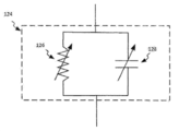
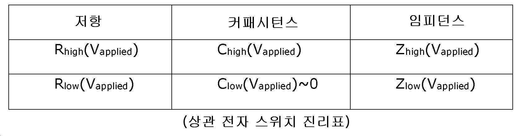
도 2는 가변 임피더 장치(124)와 같은 예시적인 가변 임피더 장치(CES 장치와 같은)의 등가 회로의 개략도를 도시한다. 언급된 바와 같이, 가변 임피더 장치(124)는 가변 저항과 가변 커패시턴스의 특성을 모두 포함할 수 있다. 예를 들어, 가변 임피더 장치에 대한 등가 회로는 일 실시 예에서 가변 커패시터(128)와 같은 가변 커패시터와 병렬인 가변 레지스터(126)과 같은 가변 레지스터를 포함할 수 있다. 가변 레지스터(126) 및 가변 커패시터(128)가 이산 컴포넌트로서 도 2에 도시되지만, 가변 임피더 장치(124)는 실질적으로 동질인 CES 엘리먼트를 동등하게 포함할 수 있고, CES 엘리먼트는 가변 커패시턴스 및 가변 저항의 특성을 포함한다. 아래의 표 1은 가변 임피더 장치(124)와 같은 예시적인 가변 임피던스 장치에 대한 예시적 진리 표를 나타낸다.FIG. 2 shows a schematic diagram of an equivalent circuit of an exemplary variable impedance device (such as a CES device), such as
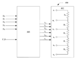
도 3은 본 발명의 일 실시 예에 따른 예시적인 설정 가능한 임피더 회로(200)의 개요를 도시한다. 회로(200)는 설정 가능한 임피더(202), 프로그래밍 회로(204), 및 제어 회로(206)를 포함한다. 일 실시 예에서, 설정 가능한 임피더(202)는 설정 가능한 임피던스를 제공하도록 배열된 복수의 상관 전자 스위치(CES)(202-1 내지 202-N)(집합적으로 복수의 CES(202)로서 지칭됨)를 포함할 수 있다. 일 예시적 구현 예에 따라, CES(202-1 내지 202-N)는 직렬로 연결되어 어레이를 형성한다. CES(202-1 내지 202-N)는 또한 임의의 다른 구성으로 배치되어 원하는 설정 가능한 임피던스 회로를 얻을 수 있음을 이해해야 한다. 도 3에 도시된 실시 예에서, 단일 프로그래밍 회로는 복수의 CES에 결합될 수 있다. 그러나, 대안적인 실시 예에서, 각 CES는 각각의 프로그래밍 회로에 결합될 수 있다.3 shows an overview of an exemplary
도 3을 다시 참조하면, 제어 회로(206)는 적어도 하나의 입력 신호(208)를 수신할 수 있다. 예를 들어, 입력 신호(208)는 복수의 CES(20) 중 하나 이상을 복수의 임피던스 상태 중 하나로 프로그래밍할 때 복수의 CES(202) 중 하나 이상에 기록될 바이너리 신호일 수 있다. 다른 예시에서, 입력 신호(208)는 복수의 CES(202) 중 각각의 하나의 CES(202)를 복수의 임피던스 상태 중 하나로 프로그래밍하는 것을 제어하기 위한 복수의 바이너리 신호를 포함할 수 있다. 일 예시에서, 임피던스 상태는 저항성 상태, 용량성 상태 또는 이들의 조합일 수 있다. 저항성 상태는 저 저항성 상태(SET 상태) 및 고 저항성 상태(RESET 상태) 중 하나일 수 있다.Referring again to FIG. 3, the
추가로 도시된 바와 같이, 프로그래밍 회로(204)는 제어 회로(206)로부터 제어 신호(210)를 수신할 수 있다. 프로그래밍 회로(204)는 제어 신호(210)에 기초하여 복수의 프로그래밍 신호(212)를 복수의 CES(202)에 제공할 수 있다. 복수의 프로그래밍 신호(208)는 복수의 임피던스 상태 중 하나에서 복수의 CES(202) 중 하나 이상을 프로그램하도록 구성될 수 있다. 일 구현 예에서, 프로그래밍 신호(212)는 입력 신호(208)에 기초하여 하나 이상의 CES(202)를 프로그램할 수 있다.As further shown, the
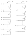
도 4는 본 발명의 일 실시 예에 따라, 복수의 CES(202)가 어떻게 설정 가능한 임피더(202)를 형성하도록 배열될 수 있는지에 대한 2개의 예시적인 구성을 도시한다. 도시된 바와 같이, 제1 구성(214)은 2개의 노드들 사이에 연결된 각 CES(R0-RN-1로 표시)를 나타낸다. 예를 들어, R0는 노드 n0과 n1 사이에 연결된 것으로 표시된다. 또한 CES에는 다른 CES와의 공통 노드가 없다. 따라서, 제1 구성(214)은 N개의 CES를 연결하는 총 2N개의 노드를 가질 수 있다. 이러한 구성에서, CES는 각 노드를 가로지르는 적절한 프로그래밍 신호를 제공함으로써 프로그램될 수 있다. 또한, 프로그래밍된 CES는 출력시 설정 가능한 임피던스 값을 얻도록 바람직한 구성으로 연결될 수 있다.Figure 4 illustrates two exemplary configurations of how a plurality of
도시된 바와 같은 제2 구성(216)은 하나의 노드가 2개의 연결된 CES들 사이에서 항상 공통이 되도록 2개의 노드들 사이의 각 CES를 연결한다. 예를 들어, CES R0은 노드 n0과 n1 사이에 연결되어 있고 R1은 노드 n1과 노드 n2 사이에 연결되어 있는 것으로 도시된다. 따라서, R0 및 R1은 공통 노드, 즉 n1을 갖는다. 따라서, 이러한 구성은 N개의 CES를 연결하기 위한 N개의 노드를 가질 수 있다.The
도 5는 본 발명의 실시 예에 따라, 복수의 CES로부터 CES를 프로그램하기 위한 예시적인 회로(300)를 도시한다. 예시된 예는 집합적으로 CES(302)로 지칭되는 N개의 CES(302-1 ... 302-N)를 포함하는 회로 배열(300)을 도시한다. 예시에서, CES(302)는 도 4에서 제2 구성(216)에 의해 도시된 바와 같이 전기적으로 배열될 수 있다.5 illustrates an
각각의 CeRAM 엘리먼트(302)는 집합적으로 프로그래밍 회로(304)로 지칭되는 프로그래밍 회로(304)(304-1 ... 304-N으로 표시)로 결합된다. 도시된 바와 같이, 각각의 프로그래밍 회로(304)는 노드(1), 노드(2), 노드(N)까지 표시된 각각의 노드들을 통해 논리 회로(306)에 결합될 수 있다. 논리 회로(306)는 디코더(308) 및 OR 게이트 어레이(310)를 포함할 수 있다. 일 구현 예에서, 디코더(308)는 log2N 입력을 수신할 수 있다. 디코더(308)는 log2N 입력들에 기초하여 N 개의 디지털 출력들을 생성할 수 있다. N 개의 디지털 출력은 OR 게이트 어레이(310)에 N 개의 입력으로서 공급될 수 있다. OR 게이트 어레이(310)는 N 개의 입력에 기초하여 N 개의 선택 신호를 생성할 수 있다.Each
각 프로그래밍 회로(304-N)는 제1 구동 회로(312-N) 및 제2 구동 회로(314-N)를 포함할 수 있다. 제1 구동 회로(312)는 각각의 CES를 제1 저항 상태로 프로그래밍하도록 구성될 수 있다. 제2 구동 회로(314)는 CES를 제2 저항 상태로 프로그래밍하도록 구성될 수 있다. 도시된 바와 같이, 제1 구동 회로(312)는 전송 게이트들(316, 318) 및 제1 레벨 시프터(320)를 포함한다. 유사하게, 제2 구동 회로(314)는 전송 게이트들(322, 324) 및 제2 레벨 시프터(326)를 포함한다.Each programming circuit 304-N may include a first driving circuit 312-N and a second driving circuit 314-N. The first drive circuit 312 may be configured to program each CES into a first resistance state. The second driving circuit 314 may be configured to program the CES to a second resistance state. As shown, the first drive circuit 312 includes transfer gates 316 and 318 and a first level shifter 320. Similarly, the second driver circuit 314 includes transfer gates 322 and 324 and a second level shifter 326.
일 실시 예에서, 각각의 CES(302)를 프로그램하기 위해 제1 구동 회로(312) 또는 제2 구동 회로(314) 중 하나를 활성화하는 프로그래밍 신호는 제어 회로(328)에 의해 제어될 수 있다. 제어 회로(328)는 제1 AND 게이트(330) 및 제2 AND 게이트(332)를 포함할 수 있다. 제1 AND 게이트(330)의 출력은 레벨 시프터(334)에 결합되고, 제2 AND 게이트(332)의 출력은 레벨 시프터(336)에 결합된다. 레벨 시프터(334, 336)는 CES를 원하는 임피던스 상태로 프로그래밍하기 위해 충분한 전압을 제공하도록 구성될 수 있다. 제어 회로(328)의 논리 구현 예는 표 2에 대해 더 설명된다. 일 구현 예에서, 표에 도시된 바와 같이, 데이터 입력(D_IN)은도 3을 참조하여 기술된 바와 같이 입력 신호(208)일 수 있다. 또한, P_R은 프로그램/판독 신호일 수 있다.In one embodiment, the programming signal that activates one of the first driving circuit 312 or the second driving circuit 314 to program each
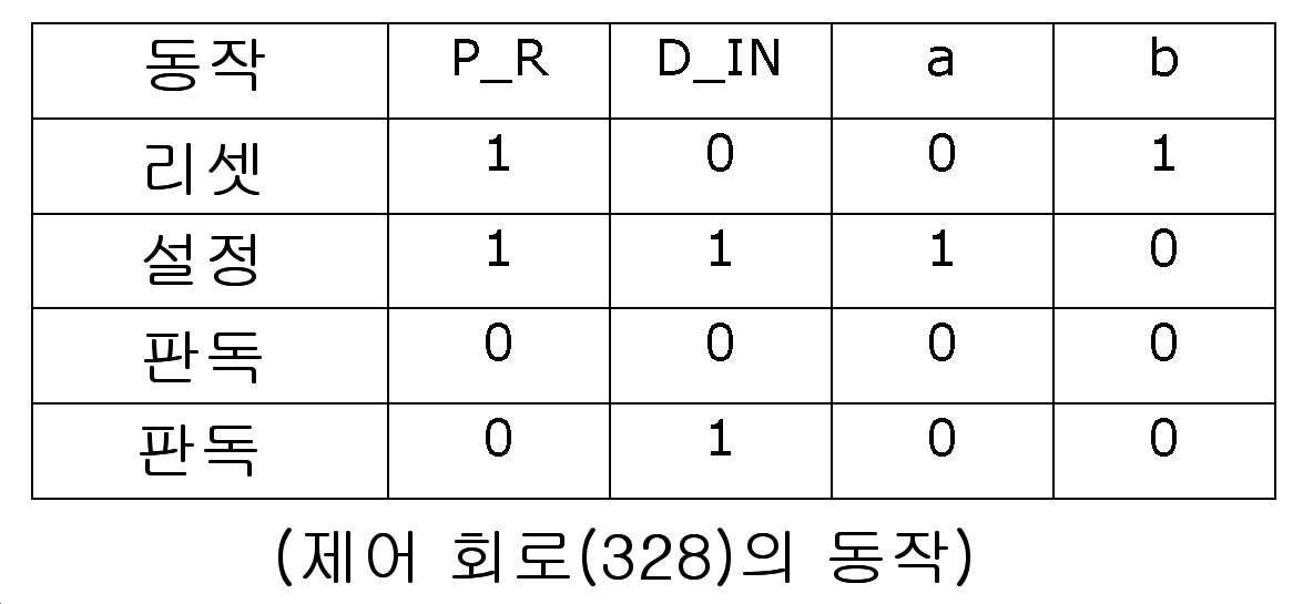
표 2에 도시된 바와 같이, CES(302)를 리셋 상태로 프로그래밍하기 위해, P_R은 논리 1로 설정될 수 있고 D_IN은 논리 0으로 설정될 수 있다. 도시된 바와 같이, AND 게이트(330)(a'로 표시됨)의 출력은 논리 0이고 AND 게이트(332)(b'로 표시됨)의 출력은 논리 1이다. 결과적으로, 전송 게이트들(322 및 324)이 활성화되고, 레벨 시프터(326)는 CES(302)를 리셋 상태, 즉 고 저항 상태로 프로그래밍하기 위해 적절한 프로그래밍 신호(예를 들어, 적절한 전압 및/또는 전류)를 제공한다.To program the
또한, CES(302)를 설정 상태, 즉 저 저항 상태로 프로그래밍하기 위해, P_R을 논리 1로 설정하고 D_IN을 논리 1로 설정할 수도 있다. 상기 표에 기초하여, AND 게이트(330)의 출력은 논리 1로 주어지고, AND 게이트(332)의 출력은 논리 0으로 주어진다. 따라서, 전송 게이트들(316 및 318)이 활성화되어, 레벨 시프터(320)가 CES(302)를 설정 상태, 즉 저 저항 상태로 프로그래밍하도록 적절한 프로그래밍 전압을 제공할 수 있게 한다. 표 2에 더 도시된 바와 같이, CES(302)가 판독 프로세스를 겪을 때, P_R 입력은 제어 회로(328)의 AND 게이트 모두에 대해 0으로 설정되어, 프로그래밍 회로(304)의 모든 전송 게이트를 비활성화시킨다.Further, in order to program the
도 5에 도시된 바와 같이, 각 CES(302)는 각각의 노드를 통해 프로그래밍 회로(304)에 결합된다. 일 구현 예에서, OR 게이트 어레이(310)로부터의 출력은 프로그래밍 회로들(304) 중 하나를 선택하여 각각의 CES(302)를 프로그램하여 다른 모든 CES의 저항 상태가 변경되지 않고 유지되도록 할 수 있다. 즉, CES들(304)로부터 단지 하나의 CES만이 고 저항 상태 또는 저 저항 상태로 프로그래밍될 수 있고, 다른 CES들의 저항 상태는 변하지 않게 유지될 수 있다.As shown in FIG. 5, each
도 6은 본 발명의 일 실시 예에 따른 OR 게이트 어레이(310)를 상세히 도시한다. 도시된 바와 같이, OR 게이트 어레이(310)는 N개의 OR 게이트들(310-1, 310-2, 310-3, 등등)을 포함할 수 있다. 각 OR 게이트가 도 5에서 설명된 디코더(308)와 같은 디코더로부터 신호를 수신하도록 OR 게이트가 결합된다. 예를 들어, 디코더(308)는 디코더(308)가 N 비트 출력을 선택 신호에 기초하여 OR 게이트 어레이(310)에 제공하도록 N 비트 디코더일 수 있다. 또한, OR 게이트 어레이(310)는 디코더(308)로부터의 N 비트 출력의 각 논리 비트가 각각의 OR 게이트에 의해 수신될 수 있도록 N 비트 입력(숫자 1-N으로 표시됨)을 포함할 수 있다. 일 구현 예에서, 디코더(308)의 N 비트 출력은 OR 게이트 어레이(310)의 N 비트 입력을 구동하여, 선택된 출력 위에 있는 모든 출력 단자가 하이이고 다른 출력 단자가 접지에 있도록 할 수 있다. 액티브 출력에 의해 수신된 논리 비트에 기초하여, 프로그래밍 회로(304)는 각각의 CES를 저 저항 상태 또는 고 저항 상태로 프로그래밍할 수 있다.6 illustrates an
예를 들어, CES(302-3)(도시되지 않음)가 표 2에 기초하여 고 저항 상태로 프로그램되어야한다면, P_R 신호는 논리 1로 설정될 수 있고, D_IN 신호는 논리 0으로 설정될 수 있다. 제어 회로(328)의 출력에 기초하여, 제2 구동 회로(314-3)가 활성화될 수 있다. 즉, 전송 게이트들(322-3 및 324-3)은 레벨 시프터(326-3)(미도시)가 활성화될 수 있다. 따라서, CES(302-3)는 고 저항 상태로 프로그램될 수 있다. 또한, 이를 위해, 프로그래밍 회로(304-3)(도시되지 않음)의 선택이 필요할 수 있다. 또한, 다른 모든 프로그래밍 회로의 회로 배열은 각각의 CES가 그들의 임피던스 상태를 변경하지 않을 수 있는 방식으로 선택될 수 있다. 이를 달성하기 위해, 상술한 바와 같이, 적절한 입력 신호가 디코더(308)에 공급될 수 있다. 입력 신호에 기초하여, OR 게이트 어레이(310)는 CES(302-3)가 고 저항 상태로 프로그래밍되고, 다른 모든 CES 상태는 변경되지 않게 되도록 적절한 선택 신호를 생성할 수 있다.For example, if CES 302-3 (not shown) is to be programmed to a high resistance state based on Table 2, the P_R signal may be set to logic one and the D_IN signal may be set to logic zero . Based on the output of the control circuit 328, the second driving circuit 314-3 can be activated. That is, the level shifter 326-3 (not shown) may be activated for the transfer gates 322-3 and 324-3. Thus, the CES 302-3 can be programmed to a high resistance state. Also, for this purpose, selection of a programming circuit 304-3 (not shown) may be required. In addition, the circuit arrangement of all other programming circuits may be selected in such a way that each CES may not change their impedance state. To achieve this, a suitable input signal may be supplied to the
도 7은 본 발명의 일 실시 예에 따라 다수의 CES를 동시에 프로그래밍하기 위한 회로 배열(400)을 도시한다. 도시된 바와 같이, 회로 배열(400)은 R0-R4로 도시된 바와 같이 5개의 프로그램 가능한 CES를 포함하는 설정 가능한 임피더(402)를 포함한다. CES는 각 CES가 노드를 통해 다른 CES에 결합되는 방식으로 서로 직렬로 결합될 수 있다. 노드는 na - nf에 의해 도면에 표시되어 있다. 각 노드는 노드 전압(Va - Vf)에 연결될 수 있다. 또한, 각각의 CES는 2개의 노드 사이에 연결되어 2개의 노드의 노드 전압의 차이가 CES를 가로지르는 전압 강하를 나타내도록 할 수 있다. 예를 들어, 노드 na 및 nb에 대한 노드 전압 사이의 차이는 CES R0를 가로지르는 전압 강하를 제공한다. CES를 가로지르는 전압 강하는 CES에 대한 프로그래밍 전압으로 작용한다.Figure 7 illustrates a
일 실시 예에서, 설정 가능한 임피더(402)는 프로그래밍 회로(404)에 연결되어, 설정 가능한 임피더(402)의 복수의 프로그램 가능한 CES가 프로그래밍 회로(404)로부터 수신된 신호에 기초하여 동시에 프로그래밍될 수 있도록 한다. 또한, CES가 동시에 프로그래밍되더라도, 각각의 CES는 저 저항 상태 또는 고 저항 상태로 프로그램될 수 있다. 일 구현 예에서, 프로그래밍 회로(404)는 (D0-D4로 표시되는) 복수의 데이터 입력에 기초하여 프로그래밍 가능한 신호를 설정 가능한 임피더(402)에 제공할 수 있다. 일 예시에서, 프로그램/판독 입력(P_R)은 CES를 프로그래밍하는 동안 논리 1로 유지될 수 있다. 복수의 데이터 입력은 프로그래밍 회로(402)에 공급되어 적절한 노드 전압으로 변환되어 설정 가능한 임피더(402)의 복수의 프로그램 가능한 CES를 프로그램할 수 있다. 복수의 프로그램 가능 CES를 프로그램하는데 필요한 노드 전압의 예시적인 세트는 하기의 표 3에 주어진다.In one embodiment, the
표 3에 도시된 바와 같이, 각각의 노드에는 특정 노드 전압이 제공될 수 있지만, 도시된 전압은 단지 예시적이고 비한정적인 것으로 이해될 것이다. 일례에 도시된 바와 같이, 각 CES에 대해, CES는 대응 디지털 입력 신호가 논리 0에 있을 때 고 저항 상태로 프로그램될 수 있고, 대응 디지털 입력 신호가 논리 1에 있을 때 저 저항 상태로 프로그래밍될 수 있다. 이 예는 단지 예시적인 목적으로 설명되며, 논리 0은 저 저항 상태로 표현될 수 있고 논리 1은 고 저항 상태로 표시될 수 있다. 이 경우 노드 전압이 그에 따라 생성된다. 또한, 설정 상태에서 CES를 프로그램하기 위해 대략 1.2 볼트의 전압(Vset)이 요구될 수 있고 리셋 상태에서 CES를 프로그램하기 위해 대략 0.6 볼트의 전압(Vreset)이 필요할 수 있다고 가정될 수 있다.As shown in Table 3, each node may be provided with a particular node voltage, but the voltages shown are to be understood as being exemplary and non-limiting. As shown in the example, for each CES, the CES can be programmed to the high resistance state when the corresponding digital input signal is at
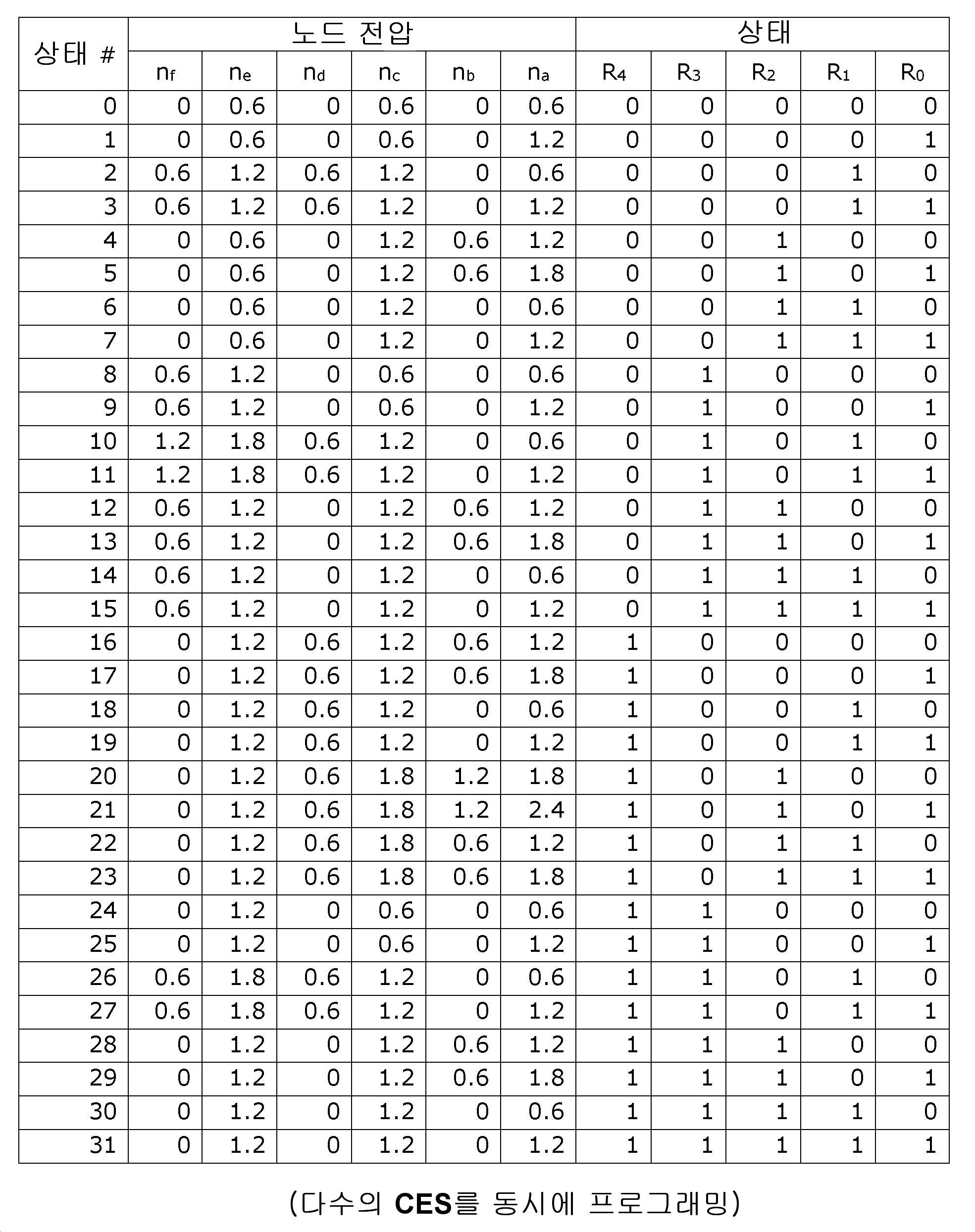
도 7을 다시 참조하면, 2개의 노드의 노드 전압의 차이가 CES를 가로지르는 전압 강하를 나타내도록 각 CES가 2개의 노드 사이에 연결될 수 있다. 예를 들어, 노드 na 및 nb에 대한 노드 전압 사이의 차이는 CES R0를 가로지르는 전압 강하를 제공한다. CES를 가로지르는 전압 강하는 CES에 대한 프로그래밍 전압으로 작용한다.Referring back to FIG. 7, each CES may be connected between two nodes so that the difference in node voltages of the two nodes represents a voltage drop across the CES. For example, the difference between node voltages for nodes n a and n b provides a voltage drop across CES R 0 . The voltage drop across the CES acts as the programming voltage for the CES.
표 3에 도시된 예시에서, 상태 # 0은 각각의 CES가 고 저항 상태에 있음을 나타낸다. 상태 # 0에서 프로그래밍되는 CES의 경우, 노드 na-nf에 대해 해당하는 노드 전압은 각각 0.6V, 0V, 0.6V, 0V, 0.6V 및 0V로 표시된다. 상태 # 1에서 R0은 저 저항 상태에 있고 다른 모든 CES는 고 저항 상태에 있다. 노드 na-nf에 대해 해당하는 노드 전압은 각각 1.2V, 0V, 0.6V, 0V, 0.6V 및 0V로 주어진다. 따라서, 노드에 인가된 적절한 노드 전압 및 노드 전류를 선택함으로써, 다수의 CES가 상이한 저항 상태로 동시에 프로그래밍될 수 있다.In the example shown in Table 3,
표 3에 도시된 바와 같이, CES에 대한 모든 상이한 프로그래밍 상태를 실현하기 위해 총 5개의 공급 전압, 즉, 0V, 0.6V, 1.2V, 1.8V 및 2.4V가 요구된다. 일 실시 예에서, 프로그래밍될 CES의 수가 홀수일 때, 프로그래밍 상태들 중 하나를 무효화함으로써 하나의 공급 전압이 절약될 수 있고, 따라서 공급 전압을 생성하는데 사용되는 회로에 대해 절약할 수 있다. 표 3을 다시 참조하면, 상태 # 21은 노드 na에서의 노드 전압을 2.4V로 나타낸다. 구현 예에서, 상태 # 21이 제거되면, 2.4 볼트의 노드 전압은 더 이상 필요하지 않을 수 있다. 따라서 노드 전압을 생성하는 데 사용되는 회로에 필요한 전력 및 면적을 절약할 수 있다. 또한, 다른 실시 예에서, 노드 na에서의 노드 전압을 2.4 볼트에서 0 볼트로 변경함으로써, R0은 여전히 저 저항 상태로 프로그램될 수 있다. 이것은 2.4V가 노드 na에 인가될 때 이전에 사용된 음의 Vset 차이보다는 노드 nb 및 na의 노드 전압에 대해 양의 Vset 전압 차를 사용함으로써 수행될 수 있다.As shown in Table 3, a total of five supply voltages, 0V, 0.6V, 1.2V, 1.8V, and 2.4V, are required to realize all the different programming states for the CES. In one embodiment, when the number of CES to be programmed is odd, one supply voltage can be saved by negating one of the programming states, thus saving on the circuit used to generate the supply voltage. Referring back to Table 3,
여기에 설명된 예는 설정 가능한 임피더를 구현하기 위해 단방향 CES를 사용하여 설명한다. 일 실시 예에서, 설정 가능한 임피더는 양방향 CES를 사용하여 구현될 수 있다. 양방향 스위칭 CES 프로그래밍은 프로그래밍 전압 및 전류의 값에만 의존하며 프로그래밍에 사용되는 전압의 극성 및 전류 방향과는 독립적이다. 프로그래밍 전압 및 전류의 극성에 대한 비종속성은 CES를 프로그래밍하기 위한 제어 구조를 단순화할 수 있다. 일 실시 예에서, 단방향 및 양방향 CES의 조합은 적절한 제어 전압 및 전류와 함께 사용될 수 있다.The example described here uses a unidirectional CES to implement a configurable impedance. In one embodiment, a configurable impoder may be implemented using a bi-directional CES. Bidirectional switching CES programming depends only on the value of the programming voltage and current and is independent of the polarity and current direction of the voltage used for programming. The non-dependence of the polarity of the programming voltage and of the current can simplify the control structure for programming the CES. In one embodiment, a combination of unidirectional and bidirectional CES may be used with appropriate control voltages and currents.
일 실시 예에서, 노드 전압을 제어하기 위한 전압 제어는 멀티플렉서를 사용하여 실현될 수 있다. 일 예시에서, 다수의 CES를 동시에 프로그래밍하기 위해, 8-1 멀티플렉서가 각 노드에 결합될 수 있다. 노드 전압을 제어하기 위한 8-1 멀티플렉서에 대한 디지털 선택 신호는 아래 표 4에 자세히 나와 있다.In one embodiment, the voltage control for controlling the node voltage can be realized using a multiplexer. In one example, to simultaneously program multiple CESs, an 8-1 multiplexer may be coupled to each node. The digital selection signals for the 8-1 multiplexer to control the node voltage are detailed in Table 4 below.
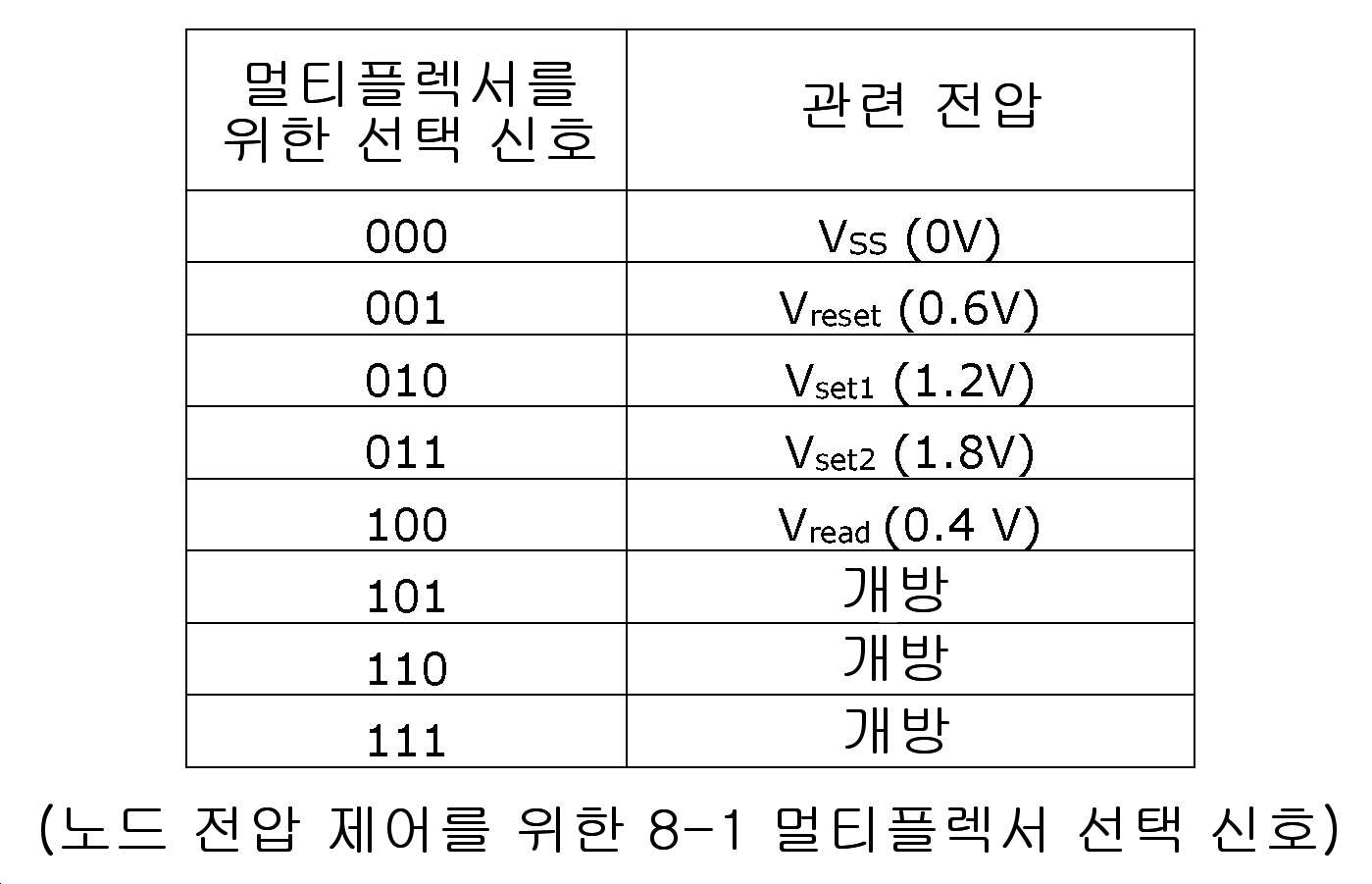
표 4에 나타낸 바와 같이, 8-1 멀티플렉서는 다수의 CES를 동시에 프로그래밍하는데 필요한 4개의 상이한 전압을 제공할 수 있지만, 도시된 전압은 단지 예시이고 비제한적인 것을 이해할 것이다. 일 구현 예에서, 각 노드는 멀티플렉서가 노드에 필요한 노드 전압을 제공할 수 있도록 멀티플렉서에 결합될 수 있다. 예를 들어, 표 4에 기초하여, 노드에서 0.6 볼트의 노드 전압에 대해, 멀티플렉서는 바이너리 001에 의해 주어진 선택 신호를 노드에 제공할 수 있다. 유사하게, 바이너리 000은 0 볼트와 동일한 노드 전압을 제공할 수 있다. 표 5는 멀티플렉서로부터 수신된 선택 신호를 사용하여 4개의 CES가 동시에 프로그래밍되는 예를 보여준다.As shown in Table 4, the 8-1 multiplexer may provide four different voltages needed to simultaneously program multiple CESs, but it will be appreciated that the voltages shown are by way of example only and not limitation. In one implementation, each node may be coupled to a multiplexer such that the multiplexer can provide the node voltage needed by the node. For example, based on Table 4, for a node voltage of 0.6 volts at a node, the multiplexer may provide the select signal given by binary 001 to the node. Similarly, binary 000 can provide the same node voltage as zero volts. Table 5 shows an example in which four CESs are simultaneously programmed using the selection signal received from the multiplexer.
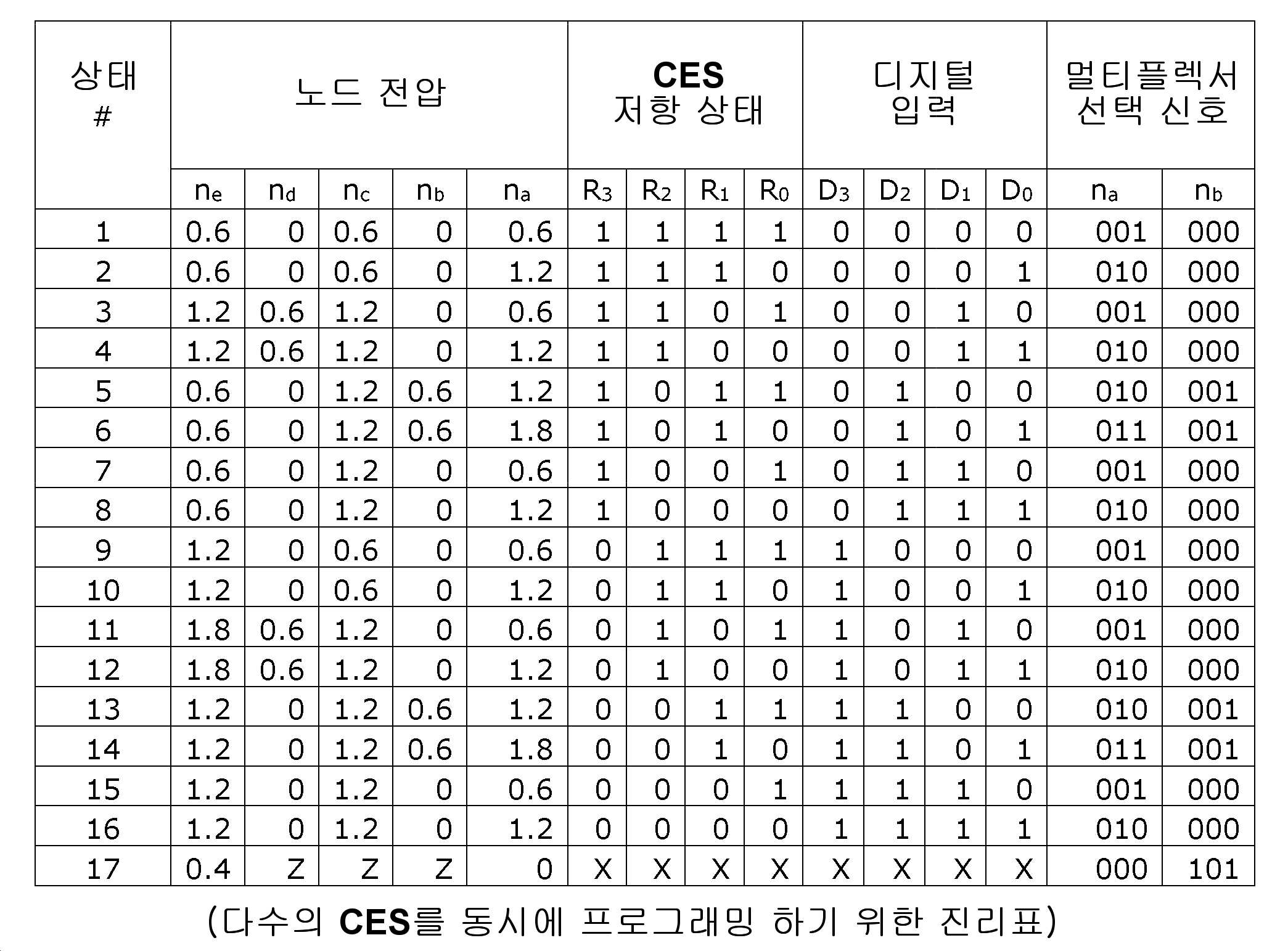
표 5에 도시된 바와 같이, 고 저항 상태 또는 저 저항 상태에서 다수의 CES를 프로그래밍하기 위해, 적절한 노드 전압을 얻기 위해 멀티플렉서로부터의 상이한 선택 신호가 각 노드에 공급될 수 있지만, 도시된 전압은 단지 예시적이고 비한정적이라는 것이 이해될 것이다. 예를 들어, 상태 # 1에 도시된 바와 같이, 4개의 CES, 즉 R0, R1, R2 및 R3 각각은 고 저항 상태로 프로그래밍된다. 또한, 표 4에 따르면, R0 엘리먼트를 고 저항 상태로 프로그래밍하기 위해, 노드 a(na)는 0.6 볼트의 노드 전압을 가져야 하고 노드 b(nb)는 0 볼트의 노드 전압을 가져야 한다. 이들 전압을 제공하기 위해, 바이너리 001의 선택 신호는 노드 na와 관련된 8-1 멀티플렉서에 공급될 수 있고, 바이너리 000의 선택 신호는 노드 nb와 관련된 8-1 멀티플렉서에 공급될 수 있다. 노드 na 및 nb상의 노드 전압은 표 4에 나타낸 방식에 기초할 수 있다. 알 수 있는 바와 같이, 바이너리 001은 0.6 볼트의 출력을 제공할 수 있고 바이너리 000은 0볼트의 출력을 제공할 수 있다. 노드 nb 및 na의 노드 전압의 차이는 CES R0를 고 저항 상태로 프로그래밍하는데 필요한 프로그래밍 전압을 제공할 수 있다. 표 5는 노드 전압을 생성하기 위해 노드 na 및 nb에 공급되는 선택 신호를 나타낸 것이다. 다른 노드들, 즉 nc, nd 및 ne에 대한 선택 신호들이 유사한 방식으로 생성될 수 있다. 또한, 다수의 CES를 동시에 프로그래밍하는 상기 배열은 서로 결합된 4개의 CES에 대하여 설명된다. 그러나, 대안적인 실시 예에서, 4개 이상의 CES가 동시에 프로그래밍될 수도 있다.As shown in Table 5, to program multiple CESs in a high-resistance state or a low-resistance state, different select signals from a multiplexer may be supplied to each node to obtain an appropriate node voltage, It will be understood that the invention is illustrative and non-limiting. For example, as shown in
일 예시에서, 판독 동작에 대해, 표 5의 상태 # 17에 도시된 바와 같이, 적절한 노드 전압이 CES에 인가될 수 있다. 도시된 바와 같이, 판독 동작에 대해, 노드 na는 0볼트의 전압이어야 하고 노드 ne는 0.4 볼트의 전압을 가져야 한다. 표 3에 도시된 방식에 기초하여, 이들 전압을 제공하기 위해, 바이너리 000의 선택 신호는 노드 na와 연관된 8-1 멀티플렉서에 공급될 수 있고, 바이너리 100의 선택 신호는 노드 ne에 연관된 8-1 멀티플렉서로 공급될 수 있다. 또한 표 5에서 "Z"로 표시된 바와 같이 다른 모든 노드는 연결이 연결해제되거나 개방될 수 있다. 또한 CES에 대한 디지털 입력 및 결과적으로 CES의 저항 상태는 표 5에서 "X"로 표시된 것처럼 모든 값을 가정할 수 있다. 일 구현 예에서, na와 ne 사이의 전압 강하가 판독될 수 있다. 다른 구현 예에서, 고정 전압이 인가될 수 있고 노드 na 및 ne 사이의 전류가 판독될 수 있다.In one example, for a read operation, an appropriate node voltage may be applied to the CES, as shown in state # 17 of Table 5. [ As shown, for the read operation, node n a should be a voltage of zero volts and node n e should have a voltage of 0.4 volts. Based on the method shown in Table 3, to provide these voltages, a selection signal of the binary 000 may be supplied to the 8-1 multiplexer associated with the node n a, a binary selection signal 100 is associated with the node n e 8 -1 < / RTI > multiplexer. Also, all other nodes can be disconnected or opened as indicated by the "Z" in Table 5. Also, the digital input to the CES and consequently the resistance state of the CES can assume all values as indicated by the "X" in Table 5. In one implementation, the voltage drop between n a and n e can be read. In another embodiment, a fixed voltage can be applied and the current between nodes n a and n e can be read.
일 실시 예에서, 디지털 논리 변환은 다수의 CES를 프로그래밍하기 위해 상기 표로부터 프로그래밍 회로를 생성하는데 사용될 수 있다. 다른 실시 예에서, 노드 전압에 대한 전압 제어는 레지스터-전달 로직(RTL: register-transfer logic)에 내장될 수 있다. 이러한 구현 예에서 제어는 "항상" RTL 블록에 내장되고, 조건부 "if" 및/또는 "switch"문에 의해 시작될 수 있다.In one embodiment, the digital logic transformation can be used to generate a programming circuit from the table to program multiple CESs. In another embodiment, the voltage control for the node voltage may be embedded in register-transfer logic (RTL). In this implementation, control is built into the "always" RTL block and can be initiated by conditional "if" and / or "switch" statements.
도 8은 본 발명의 일 실시 예에 따라, 설정 가능한 임피더를 프로그램하기 위한 예시적인 방법(500)을 도시한다. 상기 방법은 설정 가능한 임피더를 형성하도록 배치된 복수의 CES를 제공함으로써 시작될 수 있다. 일 예시에서, 복수의 CES는 도 3 및 도 4에 도시된 구성 중 하나에 배치될 수 있다. 또한, 일 실시 예에서, 구성 가능한 임피더는 복수의 CES를 포함하는 프로그램 가능한 레지스터 체인일 수 있다. 또한, 복수의 CES 각각은 복수의 임피던스 상태 중 하나로 구성될 수 있다. 복수의 임피던스 상태는 저항 상태, 용량성 상태, 또는 이들의 조합을 포함할 수 있다. 저항 상태는 고 저항 상태와 저 저항 상태를 포함할 수 있다. 용량성 상태는 고 용량성 상태 및 저 용량성 상태를 포함할 수 있다.Figure 8 illustrates an exemplary method 500 for programming a configurable emitter, in accordance with one embodiment of the present invention. The method may be initiated by providing a plurality of CESs arranged to form a configurable impedance. In one example, a plurality of CESs can be placed in one of the configurations shown in Figures 3 and 4. [ Further, in one embodiment, the configurable impedance may be a chain of programmable registers comprising a plurality of CESs. Also, each of the plurality of CESs may be configured as one of a plurality of impedance states. The plurality of impedance states may include a resistance state, a capacitive state, or a combination thereof. The resistance state may include a high resistance state and a low resistance state. The capacitive state may include a high capacitive state and a low capacitive state.
상기 방법은 적어도 하나의 입력 신호를 수신함으로써 시작한다(단계 800). 선택적으로, 여기에 설명된 바와 같이, 임피더의 임피던스 상태를 구성하는 프로그래밍 신호는 적어도 하나의 입력 신호에 따르거나, 제어 신호(이는 적어도 하나의 입력 신호에 종속적임)에 따를 수 있다. 따라서, 선택적으로, 제어 신호가 제공될 수 있다(단계 802). 이 방법은 입력 신호 또는 제어 신호에 따르는 프로그래밍 신호를 판정하는 단계를 포함한다(단계 804). 일단 판정되면, 프로그래밍 신호는 상기 또는 각 CES의 임피던스 상태를 구성하기 위해 상기 임피더를 형성하는 복수의 CES 중 적어도 하나의 CES에 인가된다(단계 806). 선택적으로, 하나 이상의 CES의 임피던스 상태는 프로그래밍 신호가 인가되는 동안 일정하게 유지되거나 변경되지 않고 유지된다(단계 810). CES는 적어도 하나의 입력 신호에 따라 임피던스 상태로 프로그래밍된다(단계 812). 일 예시에서, 입력 신호는 디지털 입력 신호일 수 있다. 예를 들어, 디지털 입력 신호가 논리 0일 때, 대응하는 CES가 저 임피던스 상태로 프로그래밍될 수 있고(프로그래밍 신호를 인가함으로써), 디지털 입력 신호가 논리 1일 때, 대응하는 CES가 고 임피던스 상태로 프로그래밍될 수 있다(프로그래밍 신호를 인가함으로써).The method begins by receiving at least one input signal (step 800). Alternatively, as described herein, the programming signal that constitutes the impedance state of the impedance may be in accordance with at least one input signal, or may be in accordance with a control signal, which is dependent on at least one input signal. Thus, optionally, a control signal may be provided (step 802). The method includes determining a programming signal in accordance with an input signal or a control signal (step 804). Once determined, a programming signal is applied to at least one of the plurality of CESs forming the impedance to configure the impedance state of the or each CES (step 806). Optionally, the impedance state of the one or more CESs remains constant or unchanged while the programming signal is applied (step 810). The CES is programmed to an impedance state according to at least one input signal (step 812). In one example, the input signal may be a digital input signal. For example, when the digital input signal is
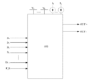
도 9는 본 발명의 일 실시 예에 따른 예시적인 디지털-아날로그 컨버터(DAC)(600)를 도시한다. 일 구현 예에서, DAC는 함께 결합된 N개의 CES(도시되지 않음)를 포함할 수 있다. N개의 CES는 도 3 또는 도 4에 도시된 임의의 하나의 구성을 사용하여 서로 결합될 수 있다.FIG. 9 illustrates an exemplary digital-to-analog converter (DAC) 600 in accordance with one embodiment of the present invention. In one implementation, the DAC may include N CES (not shown) coupled together. The N CESs can be combined with each other using any one of the configurations shown in FIG. 3 or FIG.
DAC(600)는 D0-DN -1로 표시된 N개의 데이터 입력을 더 포함할 수 있다. 데이터 입력은 디지털 입력 신호에 연결될 수 있다. 디지털 입력 신호는 바이너리일 수 있다. 또한, 프로그램/판독(P_R) 입력은 대응하는 디지털 입력 신호에 따라 복수의 CES를 프로그램하거나 또는 DAC(600)의 아날로그 신호의 적어도 하나의 출력(예를 들어, OUT+ 및 OUT-에서의 차동 출력 신호)을 판독하도록 제공될 수 있다. 예를 들어, P_R 입력이 바이너리 1로 설정되면, 기록 프로세스가 수행될 수 있고, P_R 입력이 바이너리 0으로 설정될 때, 판독 프로세스가 수행될 수 있다. 또한, CES를 프로그래밍하는데 필요한 V0-VK로 표시된 적절한 전압 소스가 제공될 수 있다. 유사하게, I0-IL로 표시된 적절한 전류 소스가 제공될 수 있다. 일 예시에서 적절한 전압 및 전류는 도 7에 설명된 8-1 멀티플렉서를 사용하여 제공될 수 있다.The
일 구현 예에서, 판독 프로세스 동안, 고정된 전류 값이 제1 노드 및 최종 노드(예를 들어, 각각 n0 및 nN)를 통해 모든 CES로부터 전달될 수 있다. 또한, 다른 모든 노드는 "연결해제" 상태에 연결될 수 있으며, 제1 노드와 마지막 노드 사이의 전압 강하가 판독될 수 있다. 다른 구현 예에서, 고정 전압이 설정될 수 있고 제1 노드 및 최종 노드를 통과하는 전류가 측정될 수 있다. 측정된 전류 또는 전압의 값은 예를 들어 아날로그 출력 핀(OUT+ 및 OUT-으로 표시)에 제공될 수 있다.In one implementation, during the read process, a fixed current value may be delivered from all CES through the first node and the last node (e.g., n 0 and n N , respectively). In addition, all other nodes may be connected to the "disconnected" state, and the voltage drop between the first node and the last node may be read. In another implementation, a fixed voltage can be set and the current passing through the first node and the last node can be measured. The measured current or voltage values may be provided, for example, on analog output pins (labeled OUT + and OUT-).
도 10은 본 발명의 일 실시 예에 따른 예시적인 메모리 어레이(700)를 도시한다. 이 경우, 메모리 어레이(700)는 데이터를 아날로그 포맷으로 저장한다. 메모리 어레이(700)는 도시된 바와 같이 N 비트 셀을 포함할 수 있다. 각 비트 셀은 설정 가능한 레지스터 체인을 형성하기 위해 노드 사이(예를 들어, na-ne)에 연결된 CES 세트(예를 들어, R0-R3)를 포함할 수 있다. 메모리 어레이(700)의 비트 셀들을 프로그래밍하기 위해, 디지털 데이터는 노드 전압들에 기초하여 CES에 의해 형성되고, 따라서 각각의 비트 셀 내에 형성된 설정 가능한 레지스터 체인의 레지스터 값의 형태로 디지털 데이터가 프로그램 가능 CES들 내에 저장될 수 있도록 적절한 노드 전압들(Va-Ve)로 변환될 수 있고 노드들에 공급될 수 있다. 설정 가능한 레지스터 체인은 상술한 실시 예 중 하나를 사용하여 프로그래밍될 수 있다. 따라서, 메모리 어레이(700)는 비트 셀 내에 데이터를 저장하기 위해 다수의 CES의 동시 프로그래밍을 사용할 수 있다.Figure 10 illustrates an exemplary memory array 700 in accordance with one embodiment of the present invention. In this case, the memory array 700 stores the data in an analog format. The memory array 700 may include N-bit cells as shown. Each bit cell may include a set of CESs (e.g., R 0 -R 3 ) connected between nodes (e.g., n a -n e ) to form a configurable register chain. To program the bit cells of the memory array 700, the digital data is formed by the CES based on the node voltages, so that the digital data is programmable in the form of register values in a configurable register chain formed within each bit cell May be converted to appropriate node voltages (V a -V e ) to be stored in the CESs and supplied to the nodes. The settable register chain can be programmed using one of the embodiments described above. Thus, the memory array 700 can use multiple simultaneous programming of CES to store data in bit cells.
일 실시 예에서, 디지털 데이터가 비트 셀 내에 기록될 때, 프로그램/판독 신호(P_R)는 바이너리 1에 있을 수 있고, 디지털 데이터가 비트 셀로부터 판독될 때, P_R 신호는 바이너리 0에 있을 수 있다. 상기에서 기술된 바와 같이, 데이터는 비트 셀로부터 아날로그 데이터로서 판독될 수 있다. 또한, 제어 엘리먼트(702)는 메모리 어레이(700) 내의 데이터 저장을 제어할 수 있다.In one embodiment, when digital data is written into the bit cell, the program / read signal P_R may be in
본 개시물의 예시적인 실시 예가 첨부된 도면을 참조하여 본원에 상세히 설명되었지만, 본 개시물은 이들 정확한 실시 예에 한정되지 않고 다양한 변경 및 수정이 첨부된 청구범위에 의해 정의된 바와 같은 본 개시물의 취지 및 범위를 벗어나지 않고 당업자에 의해 이루어질 수 있음을 이해해야 한다.While the exemplary embodiments of this disclosure have been described in detail herein with reference to the accompanying drawings, it is to be understood that the disclosure is not limited to these precise embodiments, and that various changes and modifications may be effected within the spirit and scope of the invention as defined by the appended claims. It will be understood by those skilled in the art that various changes in form and details may be made therein without departing from the spirit and scope of the invention.
Claims (17)
적어도 하나의 입력 신호에 각각 따르는 복수의 프로그래밍 신호를 제공하도록 구성된 적어도 하나의 프로그래밍 회로로서, 상기 각각의 프로그래밍 신호는 CES의 임피던스 상태를 구성하는 상기 프로그래밍 회로;
를 포함하는 것을 특징으로 하는 회로.A plurality of correlated electronic switches (CES) arranged to form a configurable impedance, wherein each CES can be configured in one of a plurality of impedance states; And
At least one programming circuit configured to provide a plurality of programming signals, each programming signal corresponding to at least one input signal, wherein each programming signal comprises the programming circuitry constituting an impedance state of the CES;
≪ / RTI >
상기 CES를 상기 제1 임피던스 상태로 구성하기 위한 제1 프로그래밍 신호를 제공하는 제1 구동 회로; 및
상기 CES를 상기 제2 임피던스 상태로 구성하기 위한 제2 프로그래밍 신호를 제공하는 제2 구동 회로;
를 포함하고,
상기 제1 프로그래밍 신호 및 상기 제2 프로그래밍 신호 중 하나는 상기 적어도 하나의 입력 신호에 따르는 것을 특징으로 하는 회로.3. The method of claim 2, wherein the plurality of impedance states comprises a first impedance state and a second impedance state, each programming circuit comprising:
A first driving circuit for providing a first programming signal for configuring the CES to the first impedance state; And
A second driving circuit for providing a second programming signal for configuring the CES to the second impedance state;
Lt; / RTI >
Wherein one of the first programming signal and the second programming signal follows the at least one input signal.
상기 적어도 하나의 입력 신호를 수신하고; 및
상기 적어도 하나의 입력 신호에 따라 적어도 하나의 제어 신호를 상기 적어도 하나의 프로그래밍 회로에 제공하도록;
구성되고,
상기 적어도 하나의 프로그래밍 회로는 상기 적어도 하나의 제어 신호에 따르는 상기 복수의 프로그래밍 신호를 제공하는 것을 특징으로 하는 회로.5. The control circuit according to any one of claims 1 to 4, further comprising a control circuit, the control circuit comprising:
Receive the at least one input signal; And
Provide at least one control signal to the at least one programming circuit in accordance with the at least one input signal;
Respectively,
Wherein the at least one programming circuit provides the plurality of programming signals in accordance with the at least one control signal.
적어도 하나의 입력 신호를 수신하는 단계;
상기 적어도 하나의 입력 신호에 따르는 적어도 하나의 프로그래밍 신호를 판정하는 단계로서, 상기 프로그래밍 신호 또는 상기 각각의 프로그래밍 신호는 상기 복수의 CES 중 하나 이상의 CES의 임피던스 상태를 구성하는 상기 판정하는 단계; 및
상기 CES 또는 각각의 CES의 상기 임피던스 상태를 구성하기 위해 상기 프로그래밍 신호를 상기 복수의 CES 중 하나 이상의 CES에 인가하는 단계;
를 포함하는 것을 특징으로 하는 설정 가능한 임피더의 임피던스를 구성하는 방법.CLAIMS What is claimed is: 1. A method of configuring an impedance of a configurable impedance including a plurality of correlated electronic switches (CES)
Receiving at least one input signal;
Determining at least one programming signal that follows the at least one input signal, wherein the programming signal or each programming signal comprises an impedance state of at least one of the plurality of CESs; And
Applying the programming signal to at least one of the plurality of CESs to configure the impedance state of the CES or each CES;
≪ / RTI > wherein the impedance of the settable impedance is set to a predetermined value.
복수의 디지털 입력 신호를 수신하도록 구성된 복수의 데이터 입력;
복수의 상관 전자 스위치(CES) 중 각각의 CES가 상기 복수의 디지털 입력 신호에 따르는 복수의 임피던스 상태 중 하나의 임피던스 상태로 설정 가능한 복수의 CES; 및
적어도 하나의 아날로그 출력 신호를 출력하도록 구성된 적어도 하나의 출력으로서, 상기 아날로그 출력 신호 또는 각각의 아날로그 출력 신호는 상기 복수의 CES의 임피던스 상태들에 따르는 상기 적어도 하나의 출력;
을 포함하는 것을 특징으로 하는 디지털-아날로그 컨버터.In a digital-to-analog converter (DAC) circuit,
A plurality of data inputs configured to receive a plurality of digital input signals;
A plurality of CESs, each CES of the plurality of the correlating electronic switches (CES) being capable of being set to one impedance state in a plurality of impedance states corresponding to the plurality of digital input signals; And
At least one output configured to output at least one analog output signal, wherein the analog output signal or each analog output signal comprises the at least one output according to the impedance states of the plurality of CESs;
To-analog converters.
기록 신호인 적어도 하나의 입력 신호를 수신하고;
각각의 프로그래밍 신호가 CES의 상기 임피던스 상태를 구성하는, 상기 복수의 디지털 입력 신호에 따라 상기 복수의 CES에 복수의 프로그래밍 신호를 제공하도록;
구성되는 것을 특징으로 하는 디지털-아날로그 컨버터.15. The apparatus of claim 14, further comprising: a control circuit,
Receiving at least one input signal which is a recording signal;
Providing a plurality of programming signals to the plurality of CESs according to the plurality of digital input signals, wherein each programming signal constitutes the impedance state of the CES;
To-digital converters.
판독 신호인 적어도 하나의 입력 신호를 수신하고; 및
상기 적어도 하나의 아날로그 출력 신호를 출력하기 위해 상기 복수의 CES에 기준 신호를 제공하도록;
구성되는 것을 특징으로 하는 디지털-아날로그 컨버터.16. A device according to claim 14 or 15, further comprising a control circuit, said control circuit comprising:
Receiving at least one input signal that is a read signal; And
Providing a reference signal to the plurality of CESs to output the at least one analog output signal;
To-digital converters.
Applications Claiming Priority (3)
| Application Number | Priority Date | Filing Date | Title |
|---|---|---|---|
| US14/979,156 | 2015-12-22 | ||
| US14/979,156 US9773550B2 (en) | 2015-12-22 | 2015-12-22 | Circuit and method for configurable impedance array |
| PCT/GB2016/053931 WO2017109460A1 (en) | 2015-12-22 | 2016-12-14 | Circuit and method for configurable impedance array |
Publications (2)
| Publication Number | Publication Date |
|---|---|
| KR20180098309A true KR20180098309A (en) | 2018-09-03 |
| KR102673064B1 KR102673064B1 (en) | 2024-06-10 |
Family
ID=57737748
Family Applications (1)
| Application Number | Title | Priority Date | Filing Date |
|---|---|---|---|
| KR1020187020703A Active KR102673064B1 (en) | 2015-12-22 | 2016-12-14 | Circuit and method for configurable impedance array |
Country Status (5)
| Country | Link |
|---|---|
| US (3) | US9773550B2 (en) |
| KR (1) | KR102673064B1 (en) |
| CN (1) | CN108604459B (en) |
| TW (1) | TWI728020B (en) |
| WO (1) | WO2017109460A1 (en) |
Cited By (1)
| Publication number | Priority date | Publication date | Assignee | Title |
|---|---|---|---|---|
| KR20220113451A (en) * | 2020-01-28 | 2022-08-12 | 마이크론 테크놀로지, 인크. | Analog storage using memory devices |
Families Citing this family (27)
| Publication number | Priority date | Publication date | Assignee | Title |
|---|---|---|---|---|
| US9558819B1 (en) | 2015-08-13 | 2017-01-31 | Arm Ltd. | Method, system and device for non-volatile memory device operation |
| US9755146B2 (en) | 2015-09-10 | 2017-09-05 | ARM, Ltd. | Asymmetric correlated electron switch operation |
| US10797238B2 (en) | 2016-01-26 | 2020-10-06 | Arm Ltd. | Fabricating correlated electron material (CEM) devices |
| US9747982B1 (en) | 2016-02-22 | 2017-08-29 | Arm Ltd. | Device and method for generating random numbers |
| US10276795B2 (en) | 2016-08-15 | 2019-04-30 | Arm Ltd. | Fabrication of correlated electron material film via exposure to ultraviolet energy |
| US10128438B2 (en) | 2016-09-09 | 2018-11-13 | Arm Limited | CEM switching device |
| US10103327B2 (en) | 2016-09-14 | 2018-10-16 | Arm Limited | CEM switching device |
| US9978942B2 (en) | 2016-09-20 | 2018-05-22 | Arm Ltd. | Correlated electron switch structures and applications |
| US10267831B2 (en) * | 2016-09-30 | 2019-04-23 | Arm Ltd. | Process variation compensation with correlated electron switch devices |
| US9997242B2 (en) | 2016-10-14 | 2018-06-12 | Arm Ltd. | Method, system and device for non-volatile memory device state detection |
| US9899083B1 (en) | 2016-11-01 | 2018-02-20 | Arm Ltd. | Method, system and device for non-volatile memory device operation with low power high speed and high density |
| US10121967B2 (en) * | 2016-11-29 | 2018-11-06 | Arm Limited | CEM switching device |
| US9871528B1 (en) * | 2016-11-30 | 2018-01-16 | Arm Ltd. | Digital to analog conversion with correlated electron switch devices |
| US10002669B1 (en) | 2017-05-10 | 2018-06-19 | Arm Ltd. | Method, system and device for correlated electron switch (CES) device operation |
| US10211398B2 (en) | 2017-07-03 | 2019-02-19 | Arm Ltd. | Method for the manufacture of a correlated electron material device |
| GB2567215B (en) * | 2017-10-06 | 2020-04-01 | Advanced Risc Mach Ltd | Reconfigurable circuit architecture |
| US10714175B2 (en) | 2017-10-10 | 2020-07-14 | ARM, Ltd. | Method, system and device for testing correlated electron switch (CES) devices |
| US10229731B1 (en) | 2017-10-11 | 2019-03-12 | Arm Ltd. | Method, system and circuit for staggered boost injection |
| US11137919B2 (en) | 2017-10-30 | 2021-10-05 | Arm Ltd. | Initialisation of a storage device |
| US11636316B2 (en) | 2018-01-31 | 2023-04-25 | Cerfe Labs, Inc. | Correlated electron switch elements for brain-based computing |
| US10224099B1 (en) | 2018-02-06 | 2019-03-05 | Arm Ltd. | Method, system and device for error correction in reading memory devices |
| US10741246B2 (en) | 2018-04-23 | 2020-08-11 | Arm Limited | Method, system and device for integration of volatile and non-volatile memory bitcells |
| US10607659B2 (en) | 2018-04-23 | 2020-03-31 | Arm Limited | Method, system and device for integration of bitcells in a volatile memory array and bitcells in a non-volatile memory array |
| US10971229B2 (en) | 2018-04-23 | 2021-04-06 | Arm Limited | Method, system and device for integration of volatile and non-volatile memory bitcells |
| US10580489B2 (en) | 2018-04-23 | 2020-03-03 | Arm Ltd. | Method, system and device for complementary impedance states in memory bitcells |
| US11011227B2 (en) | 2018-06-15 | 2021-05-18 | Arm Ltd. | Method, system and device for non-volatile memory device operation |
| EP4345823A1 (en) * | 2022-09-30 | 2024-04-03 | IHP GmbH - Innovations for High Performance Microelectronics / Leibniz-Institut für innovative Mikroelektronik | Resistive memory subcell, resistive random access memory for in-memory-computing and in-memory-processor |
Citations (2)
| Publication number | Priority date | Publication date | Assignee | Title |
|---|---|---|---|---|
| KR20090078370A (en) * | 2006-11-08 | 2009-07-17 | 시메트릭스 주식회사 | Resistive switching integrated circuit memory, a method of forming a resistive switching memory, a method of writing to a resistive switching thin film memory component, and a method of manufacturing a nonvolatile resistive switching integrated circuit memory |
| WO2015163928A1 (en) * | 2014-04-26 | 2015-10-29 | Hewlett-Packard Development Company, L.P. | Switched memristor analog-to-digital conversion |
Family Cites Families (25)
| Publication number | Priority date | Publication date | Assignee | Title |
|---|---|---|---|---|
| KR100527559B1 (en) * | 2004-02-05 | 2005-11-09 | 주식회사 하이닉스반도체 | Non-volatile memory device using serial diode cell |
| US7298640B2 (en) | 2004-05-03 | 2007-11-20 | Symetrix Corporation | 1T1R resistive memory array with chained structure |
| US7443711B1 (en) * | 2004-12-16 | 2008-10-28 | Hewlett-Packard Development Company, L.P. | Non-volatile programmable impedance nanoscale devices |
| US7405462B2 (en) * | 2006-01-31 | 2008-07-29 | Hewlett-Packard Development Company, L.P. | FPGA architecture at conventional and submicron scales |
| US7902867B2 (en) * | 2006-04-03 | 2011-03-08 | Blaise Laurent Mouttet | Memristor crossbar neural interface |
| US7872900B2 (en) * | 2006-11-08 | 2011-01-18 | Symetrix Corporation | Correlated electron memory |
| US20080107801A1 (en) | 2006-11-08 | 2008-05-08 | Symetrix Corporation | Method of making a variable resistance memory |
| US7778063B2 (en) | 2006-11-08 | 2010-08-17 | Symetrix Corporation | Non-volatile resistance switching memories and methods of making same |
| US7639523B2 (en) | 2006-11-08 | 2009-12-29 | Symetrix Corporation | Stabilized resistive switching memory |
| JP5224241B2 (en) * | 2007-11-06 | 2013-07-03 | Nltテクノロジー株式会社 | Bidirectional shift register and display device using the same |
| US7652501B2 (en) * | 2008-01-07 | 2010-01-26 | Unity Semiconductor Corporation | Programmable logic device structure using third dimensional memory |
| WO2009140305A1 (en) * | 2008-05-12 | 2009-11-19 | Symetrix Corporation | Correlated electron material and process for making |
| US20100226163A1 (en) | 2009-03-04 | 2010-09-09 | Savransky Semyon D | Method of resistive memory programming and associated devices and materials |
| KR20120059023A (en) | 2010-11-30 | 2012-06-08 | 삼성전자주식회사 | Resistor device and digital-analog converter using the same |
| US8779407B2 (en) | 2012-02-07 | 2014-07-15 | Intermolecular, Inc. | Multifunctional electrode |
| US8686386B2 (en) | 2012-02-17 | 2014-04-01 | Sandisk 3D Llc | Nonvolatile memory device using a varistor as a current limiter element |
| US8816719B2 (en) | 2012-04-26 | 2014-08-26 | Symetrix Corporation | Re-programmable antifuse FPGA utilizing resistive CeRAM elements |
| US9735766B2 (en) | 2015-07-31 | 2017-08-15 | Arm Ltd. | Correlated electron switch |
| US9851738B2 (en) | 2015-08-13 | 2017-12-26 | Arm Ltd. | Programmable voltage reference |
| US9558819B1 (en) | 2015-08-13 | 2017-01-31 | Arm Ltd. | Method, system and device for non-volatile memory device operation |
| US9748943B2 (en) | 2015-08-13 | 2017-08-29 | Arm Ltd. | Programmable current for correlated electron switch |
| US10096361B2 (en) | 2015-08-13 | 2018-10-09 | Arm Ltd. | Method, system and device for non-volatile memory device operation |
| US9584118B1 (en) | 2015-08-26 | 2017-02-28 | Nxp Usa, Inc. | Substrate bias circuit and method for biasing a substrate |
| US10056143B2 (en) | 2015-09-08 | 2018-08-21 | Arm Ltd. | Correlated electron switch programmable fabric |
| US9589636B1 (en) | 2015-09-22 | 2017-03-07 | Arm Ltd. | Method, system and device for complementary non-volatile memory device operation |
-
2015
- 2015-12-22 US US14/979,156 patent/US9773550B2/en active Active
-
2016
- 2016-12-14 KR KR1020187020703A patent/KR102673064B1/en active Active
- 2016-12-14 CN CN201680075565.3A patent/CN108604459B/en active Active
- 2016-12-14 WO PCT/GB2016/053931 patent/WO2017109460A1/en not_active Ceased
- 2016-12-22 TW TW105142665A patent/TWI728020B/en active
-
2017
- 2017-03-08 US US15/453,721 patent/US9905295B2/en active Active
-
2018
- 2018-01-08 US US15/865,116 patent/US10381076B2/en active Active
Patent Citations (2)
| Publication number | Priority date | Publication date | Assignee | Title |
|---|---|---|---|---|
| KR20090078370A (en) * | 2006-11-08 | 2009-07-17 | 시메트릭스 주식회사 | Resistive switching integrated circuit memory, a method of forming a resistive switching memory, a method of writing to a resistive switching thin film memory component, and a method of manufacturing a nonvolatile resistive switching integrated circuit memory |
| WO2015163928A1 (en) * | 2014-04-26 | 2015-10-29 | Hewlett-Packard Development Company, L.P. | Switched memristor analog-to-digital conversion |
Cited By (1)
| Publication number | Priority date | Publication date | Assignee | Title |
|---|---|---|---|---|
| KR20220113451A (en) * | 2020-01-28 | 2022-08-12 | 마이크론 테크놀로지, 인크. | Analog storage using memory devices |
Also Published As
| Publication number | Publication date |
|---|---|
| US20180218772A1 (en) | 2018-08-02 |
| WO2017109460A1 (en) | 2017-06-29 |
| CN108604459A (en) | 2018-09-28 |
| US9773550B2 (en) | 2017-09-26 |
| US20170178724A1 (en) | 2017-06-22 |
| CN108604459B (en) | 2022-07-01 |
| US20170206963A1 (en) | 2017-07-20 |
| US9905295B2 (en) | 2018-02-27 |
| US10381076B2 (en) | 2019-08-13 |
| TWI728020B (en) | 2021-05-21 |
| TW201801082A (en) | 2018-01-01 |
| KR102673064B1 (en) | 2024-06-10 |
Similar Documents
| Publication | Publication Date | Title |
|---|---|---|
| KR102673064B1 (en) | Circuit and method for configurable impedance array | |
| CN108028065B (en) | Method, system and device for complementary non-volatile memory device operation | |
| US11355192B2 (en) | CES-based latching circuits | |
| CN108475527B (en) | Latch apparatus and method | |
| TWI772269B (en) | Method and apparatus for correlated electron switch | |
| KR101711109B1 (en) | Writing a multibit resistance-switching memory cell including a dummy resistance, resistance switching elements and diodes | |
| US8619457B2 (en) | Three-device non-volatile memory cell | |
| CN110383301A (en) | spiking neural network | |
| KR101600969B1 (en) | Write method of a cross point non-volatile memory cell with diode | |
| KR20180063122A (en) | Corresponding electronic switch programmable structure | |
| KR20180125580A (en) | Correlated electron resistive memory elements &lt; RTI ID = 0.0 &gt; | |
| CN111771214A (en) | Related electronic switching elements for brain-based computing | |
| US10777273B2 (en) | Cross-point storage array including correlated electron switches | |
| CN109891505B (en) | Selective writing in storage elements | |
| US11061852B2 (en) | Reconfigurable circuit architecture |
Legal Events
| Date | Code | Title | Description |
|---|---|---|---|
| PA0105 | International application |
Patent event date: 20180718 Patent event code: PA01051R01D Comment text: International Patent Application |
|
| PG1501 | Laying open of application | ||
| A201 | Request for examination | ||
| PA0201 | Request for examination |
Patent event code: PA02012R01D Patent event date: 20211116 Comment text: Request for Examination of Application |
|
| E902 | Notification of reason for refusal | ||
| PE0902 | Notice of grounds for rejection |
Comment text: Notification of reason for refusal Patent event date: 20230726 Patent event code: PE09021S01D |
|
| AMND | Amendment | ||
| E601 | Decision to refuse application | ||
| PE0601 | Decision on rejection of patent |
Patent event date: 20231102 Comment text: Decision to Refuse Application Patent event code: PE06012S01D Patent event date: 20230726 Comment text: Notification of reason for refusal Patent event code: PE06011S01I |
|
| X091 | Application refused [patent] | ||
| AMND | Amendment | ||
| PX0901 | Re-examination |
Patent event code: PX09011S01I Patent event date: 20231102 Comment text: Decision to Refuse Application Patent event code: PX09012R01I Patent event date: 20230914 Comment text: Amendment to Specification, etc. |
|
| PX0701 | Decision of registration after re-examination |
Patent event date: 20240426 Comment text: Decision to Grant Registration Patent event code: PX07013S01D Patent event date: 20240319 Comment text: Amendment to Specification, etc. Patent event code: PX07012R01I Patent event date: 20231102 Comment text: Decision to Refuse Application Patent event code: PX07011S01I Patent event date: 20230914 Comment text: Amendment to Specification, etc. Patent event code: PX07012R01I |
|
| X701 | Decision to grant (after re-examination) | ||
| GRNT | Written decision to grant | ||
| PR0701 | Registration of establishment |
Comment text: Registration of Establishment Patent event date: 20240603 Patent event code: PR07011E01D |
|
| PR1002 | Payment of registration fee |
Payment date: 20240604 End annual number: 3 Start annual number: 1 |
|
| PG1601 | Publication of registration |