KR20180098193A - 게이트 구동회로 및 이를 포함하는 표시 장치 - Google Patents
게이트 구동회로 및 이를 포함하는 표시 장치 Download PDFInfo
- Publication number
- KR20180098193A KR20180098193A KR1020180098255A KR20180098255A KR20180098193A KR 20180098193 A KR20180098193 A KR 20180098193A KR 1020180098255 A KR1020180098255 A KR 1020180098255A KR 20180098255 A KR20180098255 A KR 20180098255A KR 20180098193 A KR20180098193 A KR 20180098193A
- Authority
- KR
- South Korea
- Prior art keywords
- transistor
- node
- signal
- gate
- channel length
- Prior art date
- Legal status (The legal status is an assumption and is not a legal conclusion. Google has not performed a legal analysis and makes no representation as to the accuracy of the status listed.)
- Granted
Links
- 230000004044 response Effects 0.000 claims abstract description 38
- 230000001419 dependent effect Effects 0.000 claims abstract 2
- 238000000034 method Methods 0.000 claims description 29
- 238000007599 discharging Methods 0.000 claims description 7
- 239000004065 semiconductor Substances 0.000 claims description 5
- 230000008569 process Effects 0.000 description 12
- 238000010586 diagram Methods 0.000 description 10
- 239000004973 liquid crystal related substance Substances 0.000 description 10
- 230000000052 comparative effect Effects 0.000 description 8
- 238000005530 etching Methods 0.000 description 7
- 229920002120 photoresistant polymer Polymers 0.000 description 7
- 230000002093 peripheral effect Effects 0.000 description 5
- 239000003990 capacitor Substances 0.000 description 4
- 108010000722 Excitatory Amino Acid Transporter 1 Proteins 0.000 description 3
- 102100031563 Excitatory amino acid transporter 1 Human genes 0.000 description 3
- 230000007423 decrease Effects 0.000 description 3
- 101000974356 Homo sapiens Nuclear receptor coactivator 3 Proteins 0.000 description 2
- 101000912503 Homo sapiens Tyrosine-protein kinase Fgr Proteins 0.000 description 2
- 102100037226 Nuclear receptor coactivator 2 Human genes 0.000 description 2
- 102100022883 Nuclear receptor coactivator 3 Human genes 0.000 description 2
- 230000008859 change Effects 0.000 description 2
- 230000006872 improvement Effects 0.000 description 2
- 238000004519 manufacturing process Methods 0.000 description 2
- 239000000758 substrate Substances 0.000 description 2
- 230000001360 synchronised effect Effects 0.000 description 2
- 238000001039 wet etching Methods 0.000 description 2
- 229910021417 amorphous silicon Inorganic materials 0.000 description 1
- 230000008878 coupling Effects 0.000 description 1
- 238000010168 coupling process Methods 0.000 description 1
- 238000005859 coupling reaction Methods 0.000 description 1
- 230000003247 decreasing effect Effects 0.000 description 1
- 238000001312 dry etching Methods 0.000 description 1
- 238000005516 engineering process Methods 0.000 description 1
- 239000011521 glass Substances 0.000 description 1
- 239000002184 metal Substances 0.000 description 1
- 238000000926 separation method Methods 0.000 description 1
- 238000002834 transmittance Methods 0.000 description 1
- 230000004304 visual acuity Effects 0.000 description 1
Images


Classifications
-
- G—PHYSICS
- G09—EDUCATION; CRYPTOGRAPHY; DISPLAY; ADVERTISING; SEALS
- G09G—ARRANGEMENTS OR CIRCUITS FOR CONTROL OF INDICATING DEVICES USING STATIC MEANS TO PRESENT VARIABLE INFORMATION
- G09G3/00—Control arrangements or circuits, of interest only in connection with visual indicators other than cathode-ray tubes
- G09G3/20—Control arrangements or circuits, of interest only in connection with visual indicators other than cathode-ray tubes for presentation of an assembly of a number of characters, e.g. a page, by composing the assembly by combination of individual elements arranged in a matrix no fixed position being assigned to or needed to be assigned to the individual characters or partial characters
- G09G3/34—Control arrangements or circuits, of interest only in connection with visual indicators other than cathode-ray tubes for presentation of an assembly of a number of characters, e.g. a page, by composing the assembly by combination of individual elements arranged in a matrix no fixed position being assigned to or needed to be assigned to the individual characters or partial characters by control of light from an independent source
- G09G3/36—Control arrangements or circuits, of interest only in connection with visual indicators other than cathode-ray tubes for presentation of an assembly of a number of characters, e.g. a page, by composing the assembly by combination of individual elements arranged in a matrix no fixed position being assigned to or needed to be assigned to the individual characters or partial characters by control of light from an independent source using liquid crystals
- G09G3/3611—Control of matrices with row and column drivers
- G09G3/3674—Details of drivers for scan electrodes
- G09G3/3677—Details of drivers for scan electrodes suitable for active matrices only
-
- G—PHYSICS
- G11—INFORMATION STORAGE
- G11C—STATIC STORES
- G11C19/00—Digital stores in which the information is moved stepwise, e.g. shift registers
- G11C19/28—Digital stores in which the information is moved stepwise, e.g. shift registers using semiconductor elements
-
- H—ELECTRICITY
- H03—ELECTRONIC CIRCUITRY
- H03K—PULSE TECHNIQUE
- H03K17/00—Electronic switching or gating, i.e. not by contact-making and –breaking
- H03K17/51—Electronic switching or gating, i.e. not by contact-making and –breaking characterised by the components used
- H03K17/56—Electronic switching or gating, i.e. not by contact-making and –breaking characterised by the components used by the use, as active elements, of semiconductor devices
- H03K17/687—Electronic switching or gating, i.e. not by contact-making and –breaking characterised by the components used by the use, as active elements, of semiconductor devices the devices being field-effect transistors
- H03K17/693—Switching arrangements with several input- or output-terminals, e.g. multiplexers, distributors
Landscapes
- Engineering & Computer Science (AREA)
- Chemical & Material Sciences (AREA)
- Crystallography & Structural Chemistry (AREA)
- Physics & Mathematics (AREA)
- Computer Hardware Design (AREA)
- General Physics & Mathematics (AREA)
- Theoretical Computer Science (AREA)
- Control Of Indicators Other Than Cathode Ray Tubes (AREA)
Abstract
Description
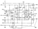
도 2는 도 1에 도시된 스테이지에 대한 등가 회로도이다.
도 3a 및 도 3b는 도 2에 도시된 트랜지스터의 평면도 및 단면도이다.
도 4는 도 2에 도시된 스테이지의 입출력 신호의 파형도들이다.
도 5a 내지 도 5d는 도 4의 부스트 업 구간에 대한 트랜지스터들의 동작을 설명하기 위한 개념도들이다.
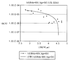
도 6은 도 2에 도시된 트랜지스터의 채널 길이에 대한 드레인-소스 전류에 대한 그래프이다.
도 7a 및 도 7b는 도 2에 도시된 트랜지스터의 제조 공정에 따른 채널 길이 및 드레인-소스 전류를 설명하기 위한 그래프이다.
도 8은 도 2에 도시된 스테이지에 따른 Q 노드의 신호 및 게이트 신호가 개선됨을 설명하기 위한 그래프이다.
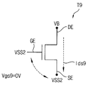
도 9는 본 발명의 다른 실시예에 따른 스테이지의 등가 회로도이다.
도 10a 내지 도 10e는 부스트 업 구간에서 도 9에 도시된 트랜지스터들의 동작을 설명하기 위한 개념도들이다.
400 : 소스 구동회로 500 : 인쇄회로기판
SRCn : 제n 스테이지 210 : 버퍼부
220 : 충전부 230 : 게이트 출력부
240 : 캐리부 250 : 인버팅부
260 : 제1 노드 제어부 270 : 제2 노드 제어부
280 : 제3 노드 제어부 290 : 제4 노드 제어부
Claims (9)
- 복수의 스테이지들이 종속적으로 연결되어 복수의 게이트 신호들을 출력하는 게이트 구동회로에서, 제n(n은 자연수) 스테이지는
클럭 신호와 제n 게이트 신호를 출력하는 출력 노드 사이에 연결되고 제어 노드와 연결된 게이트 전극을 포함하는 제1 트랜지스터를 포함하는 게이트 출력부;
상기 클럭 신호와 제n 캐리 신호를 출력하는 캐리 노드 사이에 연결된 캐리부;
상기 출력 노드와 제1 로우 전압 사이에 연결된 제1 노드 제어부; 및
상기 제어 노드와 상기 제1 로우 전압과 다른 제2 로우 전압 사이에 연결되고 상기 제n 스테이지 다음인 제n+1 스테이지로부터 제공된 제n+1 캐리 신호를 수신하는 게이트 전극을 포함하는 제2 트랜지스터를 포함하는 제2 노드 제어부를 포함하고,
상기 제2 트랜지스터는 상기 제1 트랜지스터의 채널 길이보다 긴 채널 길이를 갖는 것을 특징으로 하는 게이트 구동회로. - 제1항에 있어서, 상기 제1 로우 전압은 제1 로우 레벨을 갖고, 상기 제2 로우 전압은 상기 제1 로우 전압의 상기 제1 로우 레벨 보다 낮은 제2 로우 레벨을 갖는 것을 특징으로 하는 게이트 구동회로.
- 제2항에 있어서, 상기 제1 로우 레벨은 상기 제n 게이트 신호의 방전 레벨에 대응하고, 상기 제2 로우 레벨은 상기 제어 노드의 방전 레벨에 대응하는 것을 특징으로 하는 게이트 구동회로.
- 제1항에 있어서, 상기 제2 트랜지스터는 상기 제어 노드의 신호를 상기 제n 스테이지 다음인 상기 제n+1 스테이지의 상기 캐리부로부터 제공된 상기 제n+1 캐리 신호에 응답하여 상기 제2 로우 전압으로 방전하는 것을 특징으로 하는 게이트 구동회로.
- 제1항에 있어서, 상기 제2 노드 제어부는
상기 제n+1 스테이지 다음인 제n+2 스테이지의 상기 캐리부로부터 제공된 제n+2 캐리 신호에 응답하여 상기 제어 노드의 신호를 상기 제2 로우 전압으로 방전하고, 상기 제1 트랜지스터의 상기 채널 길이보다 긴 채널 길이를 갖는 제6 트랜지스터를 더 포함하는 것을 특징으로 하는 게이트 구동회로. - 제5항에 있어서, 상기 제2 노드 제어부는
인버팅 노드의 신호에 응답하여 상기 제어 노드에 상기 제2 로우 전압을 제공하고, 상기 제1 트랜지스터의 상기 채널 길이보다 긴 채널 길이를 갖는 제10 트랜지스터를 더 포함하는 것을 특징으로 하는 게이트 구동회로. - 제1항에 있어서, 상기 제1 노드 제어부는
상기 출력 노드와 상기 제1 로우 전압 사이에 연결되고 상기 제n 스테이지 다음인 상기 제n+1 스테이지의 상기 캐리부로부터 제공된 상기 제n+1 캐리 신호에 연결된 게이트 전극을 포함하는 제3 트랜지스터; 및
상기 제어 노드와 상기 제1 로우 전압 사이에 연결되고 인버팅 노드와 연결된 게이트 전극을 포함하는 제4 트랜지스터를 포함하는 것을 특징으로 하는 게이트 구동회로. - 제1항에 있어서, 상기 제n 스테이지는
상기 제어 노드와 상기 제n 스테이지 이전인 제n-1 스테이지로부터 제공된 제n-1 캐리 신호 사이에 연결되고 상기 제1 트랜지스터의 상기 채널 길이보다 긴 채널 길이를 갖는 제5 트랜지스터를 포함하는 버퍼부를 더 포함하는 것을 특징으로 하는 게이트 구동회로. - 제1항에 있어서, 상기 제n 스테이지는
인버팅 노드와 상기 제2 로우 전압 사이에 연결되고 상기 제2 트랜지스터의 채널 길이 및 상기 제1 트랜지스터의 상기 채널 길이 보다 긴 채널 길이를 갖는 제6 트랜지스터를 포함하는 제3 노드 제어부를 더 포함하는 것을 특징으로 하는 게이트 구동회로.
Priority Applications (1)
| Application Number | Priority Date | Filing Date | Title |
|---|---|---|---|
| KR1020180098255A KR102012742B1 (ko) | 2018-08-22 | 2018-08-22 | 게이트 구동회로 및 이를 포함하는 표시 장치 |
Applications Claiming Priority (1)
| Application Number | Priority Date | Filing Date | Title |
|---|---|---|---|
| KR1020180098255A KR102012742B1 (ko) | 2018-08-22 | 2018-08-22 | 게이트 구동회로 및 이를 포함하는 표시 장치 |
Related Parent Applications (1)
| Application Number | Title | Priority Date | Filing Date |
|---|---|---|---|
| KR1020110091698A Division KR101893189B1 (ko) | 2011-09-09 | 2011-09-09 | 게이트 구동회로 및 이를 포함하는 표시 장치 |
Publications (2)
| Publication Number | Publication Date |
|---|---|
| KR20180098193A true KR20180098193A (ko) | 2018-09-03 |
| KR102012742B1 KR102012742B1 (ko) | 2019-08-22 |
Family
ID=63600910
Family Applications (1)
| Application Number | Title | Priority Date | Filing Date |
|---|---|---|---|
| KR1020180098255A Active KR102012742B1 (ko) | 2018-08-22 | 2018-08-22 | 게이트 구동회로 및 이를 포함하는 표시 장치 |
Country Status (1)
| Country | Link |
|---|---|
| KR (1) | KR102012742B1 (ko) |
Cited By (1)
| Publication number | Priority date | Publication date | Assignee | Title |
|---|---|---|---|---|
| WO2021254087A1 (zh) * | 2020-06-19 | 2021-12-23 | 京东方科技集团股份有限公司 | 移位寄存器、栅极驱动电路及其驱动方法 |
Citations (4)
| Publication number | Priority date | Publication date | Assignee | Title |
|---|---|---|---|---|
| US20060267912A1 (en) * | 2005-05-30 | 2006-11-30 | Lee Jong-Hwan | Shift register and display device having the same, and method thereof |
| KR20080057601A (ko) * | 2006-12-20 | 2008-06-25 | 삼성전자주식회사 | 게이트 구동회로 및 이를 갖는 표시장치 |
| US20100164854A1 (en) * | 2008-12-26 | 2010-07-01 | Kyung-Wook Kim | Gate Drive Circuit, Display Device Having the Same and Method of Manufacturing the Gate Drive Circuit |
| KR20100119119A (ko) * | 2009-04-30 | 2010-11-09 | 삼성전자주식회사 | 게이트 구동회로 |
-
2018
- 2018-08-22 KR KR1020180098255A patent/KR102012742B1/ko active Active
Patent Citations (4)
| Publication number | Priority date | Publication date | Assignee | Title |
|---|---|---|---|---|
| US20060267912A1 (en) * | 2005-05-30 | 2006-11-30 | Lee Jong-Hwan | Shift register and display device having the same, and method thereof |
| KR20080057601A (ko) * | 2006-12-20 | 2008-06-25 | 삼성전자주식회사 | 게이트 구동회로 및 이를 갖는 표시장치 |
| US20100164854A1 (en) * | 2008-12-26 | 2010-07-01 | Kyung-Wook Kim | Gate Drive Circuit, Display Device Having the Same and Method of Manufacturing the Gate Drive Circuit |
| KR20100119119A (ko) * | 2009-04-30 | 2010-11-09 | 삼성전자주식회사 | 게이트 구동회로 |
Cited By (3)
| Publication number | Priority date | Publication date | Assignee | Title |
|---|---|---|---|---|
| WO2021254087A1 (zh) * | 2020-06-19 | 2021-12-23 | 京东方科技集团股份有限公司 | 移位寄存器、栅极驱动电路及其驱动方法 |
| US11798486B2 (en) | 2020-06-19 | 2023-10-24 | Hefei Boe Joint Technology Co., Ltd. | Shift register, gate drive circuit and driving method therefor |
| US12100357B2 (en) | 2020-06-19 | 2024-09-24 | Hefei Boe Joint Technology Co., Ltd. | Shift register, gate drive circuit and driving method therefor |
Also Published As
| Publication number | Publication date |
|---|---|
| KR102012742B1 (ko) | 2019-08-22 |
Similar Documents
| Publication | Publication Date | Title |
|---|---|---|
| KR101893189B1 (ko) | 게이트 구동회로 및 이를 포함하는 표시 장치 | |
| KR101217177B1 (ko) | 게이트 구동회로 및 이를 갖는 표시 장치 | |
| KR102246726B1 (ko) | 시프트 레지스터 유닛, 게이트 구동 회로, 디스플레이 디바이스 및 구동 방법 | |
| KR101573460B1 (ko) | 게이트 구동회로 | |
| EP3611720B1 (en) | Shift register unit, gate driving circuit, and driving method | |
| KR101543281B1 (ko) | 게이트 구동회로 및 이를 구비한 표시 장치 | |
| US8957882B2 (en) | Gate drive circuit and display apparatus having the same | |
| US8456409B2 (en) | Gate drive circuit and display apparatus having the same | |
| US7289594B2 (en) | Shift registrer and driving method thereof | |
| US7233308B2 (en) | Shift register | |
| US9203395B2 (en) | Gate driver and a display device including the same | |
| KR100769396B1 (ko) | 시프트 레지스터 및 그것을 구비한 표시구동장치 | |
| KR101544051B1 (ko) | 게이트 라인 구동 방법, 이를 수행하는 게이트 라인 구동회로 및 이를 포함하는 표시장치 | |
| US20070296662A1 (en) | Gate driving circuit and display apparatus having the same | |
| US20100156474A1 (en) | Gate drive circuit and display apparatus having the same | |
| CN110120200B (zh) | 显示装置 | |
| KR20120046062A (ko) | 쉬프트 레지스터 유닛, 게이트 구동 장치 및 액정 디스플레이 | |
| JP2009049985A (ja) | 電子回路のブートストラップポイント電圧を低下する方法、及びその方法を用いた装置 | |
| WO2011162057A1 (ja) | 走査信号線駆動回路およびそれを備えた表示装置 | |
| KR101451090B1 (ko) | 두 개의 클록으로 안정적인 출력 신호를 생성하기 위한 게이트 드라이버 회로 | |
| KR102471321B1 (ko) | 게이트 구동회로 및 이를 포함하는 표시 장치 | |
| KR20080000205A (ko) | 게이트 구동회로 및 이를 포함하는 표시 장치 | |
| CN107134249A (zh) | 移位寄存单元及其驱动方法、栅极驱动电路、显示装置 | |
| KR20080104726A (ko) | 게이트 구동회로 및 이를 갖는 표시 장치 | |
| KR102309625B1 (ko) | 게이트 구동 회로, 게이트 구동 회로의 구동방법 및 이를 이용한 표시장치 |
Legal Events
| Date | Code | Title | Description |
|---|---|---|---|
| A107 | Divisional application of patent | ||
| A201 | Request for examination | ||
| PA0107 | Divisional application |
Comment text: Divisional Application of Patent Patent event date: 20180822 Patent event code: PA01071R01D Filing date: 20110909 Application number text: 1020110091698 |
|
| PA0201 | Request for examination | ||
| PG1501 | Laying open of application | ||
| E902 | Notification of reason for refusal | ||
| PE0902 | Notice of grounds for rejection |
Comment text: Notification of reason for refusal Patent event date: 20180928 Patent event code: PE09021S01D |
|
| E902 | Notification of reason for refusal | ||
| PE0902 | Notice of grounds for rejection |
Comment text: Notification of reason for refusal Patent event date: 20190313 Patent event code: PE09021S01D |
|
| E701 | Decision to grant or registration of patent right | ||
| PE0701 | Decision of registration |
Patent event code: PE07011S01D Comment text: Decision to Grant Registration Patent event date: 20190515 |
|
| GRNT | Written decision to grant | ||
| PR0701 | Registration of establishment |
Comment text: Registration of Establishment Patent event date: 20190814 Patent event code: PR07011E01D |
|
| PR1002 | Payment of registration fee |
Payment date: 20190814 End annual number: 3 Start annual number: 1 |
|
| PG1601 | Publication of registration | ||
| PR1001 | Payment of annual fee |
Payment date: 20220721 Start annual number: 4 End annual number: 4 |
|
| PR1001 | Payment of annual fee |
Payment date: 20230801 Start annual number: 5 End annual number: 5 |
|
| PR1001 | Payment of annual fee |
Payment date: 20240723 Start annual number: 6 End annual number: 6 |