KR20180095609A - Method for improving wafer flatness and bonded wafer assembly made from the method - Google Patents
Method for improving wafer flatness and bonded wafer assembly made from the method Download PDFInfo
- Publication number
- KR20180095609A KR20180095609A KR1020187020189A KR20187020189A KR20180095609A KR 20180095609 A KR20180095609 A KR 20180095609A KR 1020187020189 A KR1020187020189 A KR 1020187020189A KR 20187020189 A KR20187020189 A KR 20187020189A KR 20180095609 A KR20180095609 A KR 20180095609A
- Authority
- KR
- South Korea
- Prior art keywords
- semiconductor wafer
- layer
- warp
- bow
- strain
- Prior art date
Links
- 238000000034 method Methods 0.000 title claims abstract description 66
- 239000004065 semiconductor Substances 0.000 claims abstract description 158
- 229910004298 SiO 2 Inorganic materials 0.000 claims abstract description 9
- 238000000623 plasma-assisted chemical vapour deposition Methods 0.000 claims abstract description 8
- 235000012431 wafers Nutrition 0.000 claims description 156
- 239000000463 material Substances 0.000 claims description 29
- 230000008569 process Effects 0.000 claims description 14
- 239000000758 substrate Substances 0.000 claims description 14
- 238000000151 deposition Methods 0.000 claims description 13
- 229910052594 sapphire Inorganic materials 0.000 claims description 12
- 239000010980 sapphire Substances 0.000 claims description 12
- 230000004927 fusion Effects 0.000 claims description 4
- 229910044991 metal oxide Inorganic materials 0.000 claims description 4
- 150000004706 metal oxides Chemical group 0.000 claims description 4
- 229910052581 Si3N4 Inorganic materials 0.000 claims description 3
- HQVNEWCFYHHQES-UHFFFAOYSA-N silicon nitride Chemical group N12[Si]34N5[Si]62N3[Si]51N64 HQVNEWCFYHHQES-UHFFFAOYSA-N 0.000 claims description 3
- 150000004767 nitrides Chemical class 0.000 claims description 2
- 238000005240 physical vapour deposition Methods 0.000 claims 1
- 230000006835 compression Effects 0.000 abstract description 3
- 238000007906 compression Methods 0.000 abstract description 3
- 239000010409 thin film Substances 0.000 description 52
- 230000008021 deposition Effects 0.000 description 9
- 230000000694 effects Effects 0.000 description 8
- 239000010408 film Substances 0.000 description 8
- 230000008859 change Effects 0.000 description 7
- VYPSYNLAJGMNEJ-UHFFFAOYSA-N Silicium dioxide Chemical compound O=[Si]=O VYPSYNLAJGMNEJ-UHFFFAOYSA-N 0.000 description 6
- 238000004519 manufacturing process Methods 0.000 description 4
- 238000005259 measurement Methods 0.000 description 4
- 230000009467 reduction Effects 0.000 description 3
- 230000003247 decreasing effect Effects 0.000 description 2
- 230000007717 exclusion Effects 0.000 description 2
- 239000002184 metal Substances 0.000 description 2
- 238000000059 patterning Methods 0.000 description 2
- 238000000206 photolithography Methods 0.000 description 2
- 235000012239 silicon dioxide Nutrition 0.000 description 2
- 239000000377 silicon dioxide Substances 0.000 description 2
- 229910052814 silicon oxide Inorganic materials 0.000 description 2
- XUIMIQQOPSSXEZ-UHFFFAOYSA-N Silicon Chemical compound [Si] XUIMIQQOPSSXEZ-UHFFFAOYSA-N 0.000 description 1
- 238000010521 absorption reaction Methods 0.000 description 1
- 230000008901 benefit Effects 0.000 description 1
- 230000015572 biosynthetic process Effects 0.000 description 1
- 239000000919 ceramic Substances 0.000 description 1
- 229910010293 ceramic material Inorganic materials 0.000 description 1
- 238000000748 compression moulding Methods 0.000 description 1
- 238000005137 deposition process Methods 0.000 description 1
- 239000003989 dielectric material Substances 0.000 description 1
- 230000005496 eutectics Effects 0.000 description 1
- 239000012467 final product Substances 0.000 description 1
- 230000006872 improvement Effects 0.000 description 1
- 230000001939 inductive effect Effects 0.000 description 1
- 238000000691 measurement method Methods 0.000 description 1
- 230000007246 mechanism Effects 0.000 description 1
- 238000012986 modification Methods 0.000 description 1
- 230000004048 modification Effects 0.000 description 1
- 229910052710 silicon Inorganic materials 0.000 description 1
- 239000010703 silicon Substances 0.000 description 1
- 238000001179 sorption measurement Methods 0.000 description 1
- 238000006467 substitution reaction Methods 0.000 description 1
- -1 thickness Substances 0.000 description 1
Images


Classifications
-
- H—ELECTRICITY
- H01—ELECTRIC ELEMENTS
- H01L—SEMICONDUCTOR DEVICES NOT COVERED BY CLASS H10
- H01L21/00—Processes or apparatus adapted for the manufacture or treatment of semiconductor or solid state devices or of parts thereof
- H01L21/02—Manufacture or treatment of semiconductor devices or of parts thereof
- H01L21/02002—Preparing wafers
- H01L21/02005—Preparing bulk and homogeneous wafers
- H01L21/02035—Shaping
-
- H—ELECTRICITY
- H01—ELECTRIC ELEMENTS
- H01L—SEMICONDUCTOR DEVICES NOT COVERED BY CLASS H10
- H01L21/00—Processes or apparatus adapted for the manufacture or treatment of semiconductor or solid state devices or of parts thereof
- H01L21/02—Manufacture or treatment of semiconductor devices or of parts thereof
- H01L21/02002—Preparing wafers
-
- H—ELECTRICITY
- H01—ELECTRIC ELEMENTS
- H01L—SEMICONDUCTOR DEVICES NOT COVERED BY CLASS H10
- H01L21/00—Processes or apparatus adapted for the manufacture or treatment of semiconductor or solid state devices or of parts thereof
- H01L21/02—Manufacture or treatment of semiconductor devices or of parts thereof
- H01L21/02104—Forming layers
- H01L21/02107—Forming insulating materials on a substrate
- H01L21/02109—Forming insulating materials on a substrate characterised by the type of layer, e.g. type of material, porous/non-porous, pre-cursors, mixtures or laminates
- H01L21/02112—Forming insulating materials on a substrate characterised by the type of layer, e.g. type of material, porous/non-porous, pre-cursors, mixtures or laminates characterised by the material of the layer
- H01L21/02123—Forming insulating materials on a substrate characterised by the type of layer, e.g. type of material, porous/non-porous, pre-cursors, mixtures or laminates characterised by the material of the layer the material containing silicon
- H01L21/02164—Forming insulating materials on a substrate characterised by the type of layer, e.g. type of material, porous/non-porous, pre-cursors, mixtures or laminates characterised by the material of the layer the material containing silicon the material being a silicon oxide, e.g. SiO2
-
- H—ELECTRICITY
- H01—ELECTRIC ELEMENTS
- H01L—SEMICONDUCTOR DEVICES NOT COVERED BY CLASS H10
- H01L21/00—Processes or apparatus adapted for the manufacture or treatment of semiconductor or solid state devices or of parts thereof
- H01L21/67—Apparatus specially adapted for handling semiconductor or electric solid state devices during manufacture or treatment thereof; Apparatus specially adapted for handling wafers during manufacture or treatment of semiconductor or electric solid state devices or components ; Apparatus not specifically provided for elsewhere
- H01L21/67005—Apparatus not specifically provided for elsewhere
- H01L21/67011—Apparatus for manufacture or treatment
- H01L21/67092—Apparatus for mechanical treatment
-
- H—ELECTRICITY
- H01—ELECTRIC ELEMENTS
- H01L—SEMICONDUCTOR DEVICES NOT COVERED BY CLASS H10
- H01L22/00—Testing or measuring during manufacture or treatment; Reliability measurements, i.e. testing of parts without further processing to modify the parts as such; Structural arrangements therefor
- H01L22/20—Sequence of activities consisting of a plurality of measurements, corrections, marking or sorting steps
-
- H—ELECTRICITY
- H01—ELECTRIC ELEMENTS
- H01L—SEMICONDUCTOR DEVICES NOT COVERED BY CLASS H10
- H01L23/00—Details of semiconductor or other solid state devices
- H01L23/28—Encapsulations, e.g. encapsulating layers, coatings, e.g. for protection
- H01L23/31—Encapsulations, e.g. encapsulating layers, coatings, e.g. for protection characterised by the arrangement or shape
- H01L23/3157—Partial encapsulation or coating
- H01L23/3171—Partial encapsulation or coating the coating being directly applied to the semiconductor body, e.g. passivation layer
-
- H—ELECTRICITY
- H01—ELECTRIC ELEMENTS
- H01L—SEMICONDUCTOR DEVICES NOT COVERED BY CLASS H10
- H01L24/00—Arrangements for connecting or disconnecting semiconductor or solid-state bodies; Methods or apparatus related thereto
- H01L24/93—Batch processes
- H01L24/94—Batch processes at wafer-level, i.e. with connecting carried out on a wafer comprising a plurality of undiced individual devices
-
- H—ELECTRICITY
- H01—ELECTRIC ELEMENTS
- H01L—SEMICONDUCTOR DEVICES NOT COVERED BY CLASS H10
- H01L29/00—Semiconductor devices specially adapted for rectifying, amplifying, oscillating or switching and having potential barriers; Capacitors or resistors having potential barriers, e.g. a PN-junction depletion layer or carrier concentration layer; Details of semiconductor bodies or of electrodes thereof ; Multistep manufacturing processes therefor
- H01L29/02—Semiconductor bodies ; Multistep manufacturing processes therefor
- H01L29/12—Semiconductor bodies ; Multistep manufacturing processes therefor characterised by the materials of which they are formed
- H01L29/20—Semiconductor bodies ; Multistep manufacturing processes therefor characterised by the materials of which they are formed including, apart from doping materials or other impurities, only AIIIBV compounds
- H01L29/2003—Nitride compounds
-
- H—ELECTRICITY
- H01—ELECTRIC ELEMENTS
- H01L—SEMICONDUCTOR DEVICES NOT COVERED BY CLASS H10
- H01L29/00—Semiconductor devices specially adapted for rectifying, amplifying, oscillating or switching and having potential barriers; Capacitors or resistors having potential barriers, e.g. a PN-junction depletion layer or carrier concentration layer; Details of semiconductor bodies or of electrodes thereof ; Multistep manufacturing processes therefor
- H01L29/02—Semiconductor bodies ; Multistep manufacturing processes therefor
- H01L29/30—Semiconductor bodies ; Multistep manufacturing processes therefor characterised by physical imperfections; having polished or roughened surface
-
- H—ELECTRICITY
- H01—ELECTRIC ELEMENTS
- H01L—SEMICONDUCTOR DEVICES NOT COVERED BY CLASS H10
- H01L21/00—Processes or apparatus adapted for the manufacture or treatment of semiconductor or solid state devices or of parts thereof
- H01L21/02—Manufacture or treatment of semiconductor devices or of parts thereof
- H01L21/02104—Forming layers
- H01L21/02107—Forming insulating materials on a substrate
- H01L21/02109—Forming insulating materials on a substrate characterised by the type of layer, e.g. type of material, porous/non-porous, pre-cursors, mixtures or laminates
- H01L21/02112—Forming insulating materials on a substrate characterised by the type of layer, e.g. type of material, porous/non-porous, pre-cursors, mixtures or laminates characterised by the material of the layer
- H01L21/02123—Forming insulating materials on a substrate characterised by the type of layer, e.g. type of material, porous/non-porous, pre-cursors, mixtures or laminates characterised by the material of the layer the material containing silicon
- H01L21/0217—Forming insulating materials on a substrate characterised by the type of layer, e.g. type of material, porous/non-porous, pre-cursors, mixtures or laminates characterised by the material of the layer the material containing silicon the material being a silicon nitride not containing oxygen, e.g. SixNy or SixByNz
-
- H—ELECTRICITY
- H01—ELECTRIC ELEMENTS
- H01L—SEMICONDUCTOR DEVICES NOT COVERED BY CLASS H10
- H01L21/00—Processes or apparatus adapted for the manufacture or treatment of semiconductor or solid state devices or of parts thereof
- H01L21/02—Manufacture or treatment of semiconductor devices or of parts thereof
- H01L21/02104—Forming layers
- H01L21/02107—Forming insulating materials on a substrate
- H01L21/02109—Forming insulating materials on a substrate characterised by the type of layer, e.g. type of material, porous/non-porous, pre-cursors, mixtures or laminates
- H01L21/02112—Forming insulating materials on a substrate characterised by the type of layer, e.g. type of material, porous/non-porous, pre-cursors, mixtures or laminates characterised by the material of the layer
- H01L21/02172—Forming insulating materials on a substrate characterised by the type of layer, e.g. type of material, porous/non-porous, pre-cursors, mixtures or laminates characterised by the material of the layer the material containing at least one metal element, e.g. metal oxides, metal nitrides, metal oxynitrides or metal carbides
-
- H—ELECTRICITY
- H01—ELECTRIC ELEMENTS
- H01L—SEMICONDUCTOR DEVICES NOT COVERED BY CLASS H10
- H01L21/00—Processes or apparatus adapted for the manufacture or treatment of semiconductor or solid state devices or of parts thereof
- H01L21/02—Manufacture or treatment of semiconductor devices or of parts thereof
- H01L21/02104—Forming layers
- H01L21/02107—Forming insulating materials on a substrate
- H01L21/02225—Forming insulating materials on a substrate characterised by the process for the formation of the insulating layer
- H01L21/0226—Forming insulating materials on a substrate characterised by the process for the formation of the insulating layer formation by a deposition process
- H01L21/02263—Forming insulating materials on a substrate characterised by the process for the formation of the insulating layer formation by a deposition process deposition from the gas or vapour phase
- H01L21/02271—Forming insulating materials on a substrate characterised by the process for the formation of the insulating layer formation by a deposition process deposition from the gas or vapour phase deposition by decomposition or reaction of gaseous or vapour phase compounds, i.e. chemical vapour deposition
- H01L21/02274—Forming insulating materials on a substrate characterised by the process for the formation of the insulating layer formation by a deposition process deposition from the gas or vapour phase deposition by decomposition or reaction of gaseous or vapour phase compounds, i.e. chemical vapour deposition in the presence of a plasma [PECVD]
-
- H—ELECTRICITY
- H01—ELECTRIC ELEMENTS
- H01L—SEMICONDUCTOR DEVICES NOT COVERED BY CLASS H10
- H01L22/00—Testing or measuring during manufacture or treatment; Reliability measurements, i.e. testing of parts without further processing to modify the parts as such; Structural arrangements therefor
- H01L22/10—Measuring as part of the manufacturing process
- H01L22/12—Measuring as part of the manufacturing process for structural parameters, e.g. thickness, line width, refractive index, temperature, warp, bond strength, defects, optical inspection, electrical measurement of structural dimensions, metallurgic measurement of diffusions
-
- H—ELECTRICITY
- H01—ELECTRIC ELEMENTS
- H01L—SEMICONDUCTOR DEVICES NOT COVERED BY CLASS H10
- H01L2224/00—Indexing scheme for arrangements for connecting or disconnecting semiconductor or solid-state bodies and methods related thereto as covered by H01L24/00
- H01L2224/01—Means for bonding being attached to, or being formed on, the surface to be connected, e.g. chip-to-package, die-attach, "first-level" interconnects; Manufacturing methods related thereto
- H01L2224/02—Bonding areas; Manufacturing methods related thereto
- H01L2224/07—Structure, shape, material or disposition of the bonding areas after the connecting process
- H01L2224/08—Structure, shape, material or disposition of the bonding areas after the connecting process of an individual bonding area
- H01L2224/081—Disposition
- H01L2224/0812—Disposition the bonding area connecting directly to another bonding area, i.e. connectorless bonding, e.g. bumpless bonding
- H01L2224/08135—Disposition the bonding area connecting directly to another bonding area, i.e. connectorless bonding, e.g. bumpless bonding the bonding area connecting between different semiconductor or solid-state bodies, i.e. chip-to-chip
- H01L2224/08145—Disposition the bonding area connecting directly to another bonding area, i.e. connectorless bonding, e.g. bumpless bonding the bonding area connecting between different semiconductor or solid-state bodies, i.e. chip-to-chip the bodies being stacked
-
- H—ELECTRICITY
- H01—ELECTRIC ELEMENTS
- H01L—SEMICONDUCTOR DEVICES NOT COVERED BY CLASS H10
- H01L2224/00—Indexing scheme for arrangements for connecting or disconnecting semiconductor or solid-state bodies and methods related thereto as covered by H01L24/00
- H01L2224/80—Methods for connecting semiconductor or other solid state bodies using means for bonding being attached to, or being formed on, the surface to be connected
- H01L2224/80001—Methods for connecting semiconductor or other solid state bodies using means for bonding being attached to, or being formed on, the surface to be connected by connecting a bonding area directly to another bonding area, i.e. connectorless bonding, e.g. bumpless bonding
- H01L2224/808—Bonding techniques
- H01L2224/80801—Soldering or alloying
- H01L2224/80805—Soldering or alloying involving forming a eutectic alloy at the bonding interface
-
- H—ELECTRICITY
- H01—ELECTRIC ELEMENTS
- H01L—SEMICONDUCTOR DEVICES NOT COVERED BY CLASS H10
- H01L2224/00—Indexing scheme for arrangements for connecting or disconnecting semiconductor or solid-state bodies and methods related thereto as covered by H01L24/00
- H01L2224/80—Methods for connecting semiconductor or other solid state bodies using means for bonding being attached to, or being formed on, the surface to be connected
- H01L2224/80001—Methods for connecting semiconductor or other solid state bodies using means for bonding being attached to, or being formed on, the surface to be connected by connecting a bonding area directly to another bonding area, i.e. connectorless bonding, e.g. bumpless bonding
- H01L2224/808—Bonding techniques
- H01L2224/80894—Direct bonding, i.e. joining surfaces by means of intermolecular attracting interactions at their interfaces, e.g. covalent bonds, van der Waals forces
- H01L2224/80895—Direct bonding, i.e. joining surfaces by means of intermolecular attracting interactions at their interfaces, e.g. covalent bonds, van der Waals forces between electrically conductive surfaces, e.g. copper-copper direct bonding, surface activated bonding
-
- H—ELECTRICITY
- H01—ELECTRIC ELEMENTS
- H01L—SEMICONDUCTOR DEVICES NOT COVERED BY CLASS H10
- H01L2224/00—Indexing scheme for arrangements for connecting or disconnecting semiconductor or solid-state bodies and methods related thereto as covered by H01L24/00
- H01L2224/80—Methods for connecting semiconductor or other solid state bodies using means for bonding being attached to, or being formed on, the surface to be connected
- H01L2224/80001—Methods for connecting semiconductor or other solid state bodies using means for bonding being attached to, or being formed on, the surface to be connected by connecting a bonding area directly to another bonding area, i.e. connectorless bonding, e.g. bumpless bonding
- H01L2224/808—Bonding techniques
- H01L2224/80894—Direct bonding, i.e. joining surfaces by means of intermolecular attracting interactions at their interfaces, e.g. covalent bonds, van der Waals forces
- H01L2224/80896—Direct bonding, i.e. joining surfaces by means of intermolecular attracting interactions at their interfaces, e.g. covalent bonds, van der Waals forces between electrically insulating surfaces, e.g. oxide or nitride layers
-
- H—ELECTRICITY
- H01—ELECTRIC ELEMENTS
- H01L—SEMICONDUCTOR DEVICES NOT COVERED BY CLASS H10
- H01L2224/00—Indexing scheme for arrangements for connecting or disconnecting semiconductor or solid-state bodies and methods related thereto as covered by H01L24/00
- H01L2224/93—Batch processes
- H01L2224/94—Batch processes at wafer-level, i.e. with connecting carried out on a wafer comprising a plurality of undiced individual devices
-
- H—ELECTRICITY
- H01—ELECTRIC ELEMENTS
- H01L—SEMICONDUCTOR DEVICES NOT COVERED BY CLASS H10
- H01L23/00—Details of semiconductor or other solid state devices
- H01L23/562—Protection against mechanical damage
-
- H—ELECTRICITY
- H01—ELECTRIC ELEMENTS
- H01L—SEMICONDUCTOR DEVICES NOT COVERED BY CLASS H10
- H01L24/00—Arrangements for connecting or disconnecting semiconductor or solid-state bodies; Methods or apparatus related thereto
- H01L24/01—Means for bonding being attached to, or being formed on, the surface to be connected, e.g. chip-to-package, die-attach, "first-level" interconnects; Manufacturing methods related thereto
- H01L24/02—Bonding areas ; Manufacturing methods related thereto
- H01L24/07—Structure, shape, material or disposition of the bonding areas after the connecting process
- H01L24/08—Structure, shape, material or disposition of the bonding areas after the connecting process of an individual bonding area
-
- H—ELECTRICITY
- H01—ELECTRIC ELEMENTS
- H01L—SEMICONDUCTOR DEVICES NOT COVERED BY CLASS H10
- H01L24/00—Arrangements for connecting or disconnecting semiconductor or solid-state bodies; Methods or apparatus related thereto
- H01L24/80—Methods for connecting semiconductor or other solid state bodies using means for bonding being attached to, or being formed on, the surface to be connected
-
- H—ELECTRICITY
- H01—ELECTRIC ELEMENTS
- H01L—SEMICONDUCTOR DEVICES NOT COVERED BY CLASS H10
- H01L2924/00—Indexing scheme for arrangements or methods for connecting or disconnecting semiconductor or solid-state bodies as covered by H01L24/00
- H01L2924/30—Technical effects
- H01L2924/35—Mechanical effects
- H01L2924/351—Thermal stress
- H01L2924/3511—Warping
Landscapes
- Engineering & Computer Science (AREA)
- Microelectronics & Electronic Packaging (AREA)
- Power Engineering (AREA)
- Computer Hardware Design (AREA)
- Physics & Mathematics (AREA)
- Condensed Matter Physics & Semiconductors (AREA)
- General Physics & Mathematics (AREA)
- Manufacturing & Machinery (AREA)
- Ceramic Engineering (AREA)
- Recrystallisation Techniques (AREA)
- Chemical Vapour Deposition (AREA)
- Formation Of Insulating Films (AREA)
- Physical Vapour Deposition (AREA)
- Plasma & Fusion (AREA)
- Chemical & Material Sciences (AREA)
- Chemical Kinetics & Catalysis (AREA)
- Testing Or Measuring Of Semiconductors Or The Like (AREA)
Abstract
반도체 웨이퍼의 평탄도를 향상시키는 방법 및 이 방법으로부터 만들어진 어셈블리. 본 방법의 바람직한 실시예에서, 사전에 결정된 두께 또는 패턴을 갖는 SiO2와 같은 압축 PECVD 산화물층이 바람직하지 않은 워프 또는 보우를 갖는 반도체 웨이퍼의 제2 표면 상에 증착된다. 증착된 산화물층의 두께 또는 패턴은 반도체 웨이퍼의 측정된 워프 또는 보우에 의해 결정된다. 압축 산화물층은 반도체 웨이퍼의 제2 표면 상에 상쇄 압축력(offsetting compressive force)을 제공하여 반도체 웨이퍼의 주표면에 걸쳐 워프 및 보우를 감소시킨다.Method for improving the flatness of a semiconductor wafer and an assembly made from the method. In a preferred embodiment of the method, such as SiO 2 having a thickness or a predetermined pattern A compressed PECVD oxide layer is deposited on the second surface of the semiconductor wafer having an undesirable warp or bow. The thickness or pattern of the deposited oxide layer is determined by the measured warp or bow of the semiconductor wafer. The compression oxide layer provides an offsetting compressive force on the second surface of the semiconductor wafer to reduce warp and bow over the major surface of the semiconductor wafer.
Description
관련 출원의 상호참조Cross reference of related application
본 출원은 2015년 12월 16일에 출원된 미국 가출원 제62/268,262호의 이익을 청구한다.This application claims benefit of U.S. Provisional Application No. 62 / 268,262, filed December 16, 2015.
발명의 기술분야TECHNICAL FIELD OF THE INVENTION
본 발명은 일반적으로 반도체 제조 방법에 관한 것이다. 더욱 상세하게, 본 발명은 1) 반도체 웨이퍼 및 다이 수율을 증가시키기 위하여, 산화물 증착 기술을 이용하여 휘거나(warped) 또는 굽은(bowed) 반도체 웨이퍼의 편평도(flatness) 즉, 평탄도(planarity)를 향상시키는 방법 및 2) 이 방법으로부터 제조되는 본딩된 반도체 웨이퍼 어셈블리에 관한 것이다.The present invention generally relates to a semiconductor manufacturing method. More specifically, the present invention relates to a method of manufacturing a semiconductor wafer, comprising: 1) flatness, i.e., planarity, of a semiconductor wafer that is warped or bowed using an oxide deposition technique to increase semiconductor wafer and die yield. And 2) a bonded semiconductor wafer assembly made from the method.
산업 표준 반도체 웨이퍼, 특히, GaN-온-사파이어(GaN-on-sapphire) 반도체 웨이퍼, 기판 또는 템플릿은 포토닉 응용분야에서 일반적이지만, 표면 비평탄도를 갖는 경우가 종종 있다. 반도체 웨이퍼의 바람직하지 않은 비평탄도는 워프(warp) 및/또는 보우(bowing)로 특징지워질 수 있다. 반도체 웨이퍼에 대한 전형적인 워프 및/또는 보우(bow) 측정은 측정 방법 및 에지 익스클루젼 영역(edge exclusion region) 정의에 의해 영향을 받는다. 에지 익스클루젼 영역이 작을수록, 측정된 워프 및/또는 보우가 높다. 반도체 웨이퍼 워프 및/또는 보우는 또한 반도체 웨이퍼의 직경에 의해 영향을 받으며, 하부 기판 표준 반도체 웨이퍼 상에 성장된 에피택셜층의 두께에 의해 영향을 받는다. 반도체 웨이퍼 워프는 4-in 기판의 표면에 걸쳐 100 ㎛ 이상의 크기일 수 있으며, 그러한 비평탄도는 많은 반도체 공정에서의 장애물이다.Industrial Standard Semiconductor wafers, and particularly GaN-on-sapphire (GaN) semiconductor wafers, substrates or templates, are common in photonic applications, but often have surface critical trajectories. The undesirable unevenness of the semiconductor wafer may be characterized by warp and / or bowing. Typical warp and / or bow measurements for semiconductor wafers are affected by the measurement method and the definition of the edge exclusion region. The smaller the edge exclusion zone, the higher the warp and / or bow measured. The semiconductor wafer warp and / or bow is also affected by the diameter of the semiconductor wafer and is influenced by the thickness of the epitaxial layer grown on the underlying substrate standard semiconductor wafer. Semiconductor wafer wares may be over 100 microns in size over the surface of a 4-in substrate, which is an obstacle in many semiconductor processes.
바람직하지 않은 평탄하지 않은 반도체 웨이퍼 프로파일은 일반적으로 볼록하며, 이후의 제조 단계에서의 공정 수율을 향상시키기 위하여 그러한 비평탄도를 최소화 또는 제거하는 것이 중요하다. 표준 적용에서, 기판의 워프는 바람직하게 4-in 반도체 웨이퍼에 걸쳐 적어도 80 ㎛ 미만으로 감소되며, 워프/보우의 더 큰 감소는 후속 공정 단계에서 반도체 웨이퍼 본딩 특성을 더욱 향상시킨다.Undesirably uneven semiconductor wafer profiles are generally convex, and it is important to minimize or eliminate such unevenness trajectories in order to improve process yield in later manufacturing steps. In standard applications, the warp of the substrate is preferably reduced to less than 80 microns across the 4-in semiconductor wafer, and the greater reduction in warp / bow further improves the semiconductor wafer bonding characteristics at subsequent processing steps.
4-in. 포토닉 반도체 웨이퍼의 워프는, 예를 들어, 기계적 핸들링(예를 들어, 진공 암(vacuum arm) 또는 척(chuck)) 측면에서, Canon 스태퍼(stepper)와 같은 전형적인 전형적 포토리소그래피 스태퍼에 의해 수용되기 위해서는 80 ㎛ 미만이어야 하며, 이는 차례로 국부적인 평면 포커스(local planar focus)를 향상시킨다. 일반적으로, 반도체 웨이퍼 보우는 반도체 웨이퍼의 진공 암 픽업(예를 들어 카세트로부터)에 부정적인 영향을 미치며, 과도한 반도체 웨이퍼 워프는 반도체 웨이퍼를 척에 흡착시키는데 부정적인 영향을 미친다. 반도체 웨이퍼의 후속 공정의 개선을 위하여, 임의의 잔류 보우가 오목한 것보다는 제1 반도체 웨이퍼 상에 볼록하게 유지되는 것이 바람직하다.4-in. The warp of photonic semiconductor wafers is processed by a typical exemplary photolithographic stepper, such as, for example, a Canon stepper, on the side of mechanical handling (e.g., vacuum arm or chuck) It must be less than 80 microns in order to be accommodated, which in turn improves the local planar focus. Generally, a semiconductor wafer bow has a negative effect on vacuum arm pick-up (e.g., from a cassette) of a semiconductor wafer, and excessive semiconductor wafer warfare negatively impacts adsorption of the semiconductor wafer onto the chuck. In order to improve the subsequent processing of the semiconductor wafer, it is desirable that any residual bows remain convex on the first semiconductor wafer rather than concave.
전술한 반도체 웨이퍼의 비평탄도를 감소시키고 반도체 웨이퍼 형태 프로파일을 향상시키는 저비용 공정이 후속 반도체 웨이퍼 처리 단계에서 수율을 향상시키기 위하여 요구된다.A low cost process of reducing the unevenness of the semiconductor wafer described above and improving the semiconductor wafer shape profile is required to improve the yield in subsequent semiconductor wafer processing steps.
현존하는 반도체 제조 단계에서, 미처리 반도체 웨이퍼의 워프 및/또는 보우가 반도체 포토리소그래피 스태퍼 및 반도체 웨이퍼 본딩 장치에 의한 처리 전에 가능한 한 낮은 것이 일반적으로 바람직하다.In existing semiconductor manufacturing steps, it is generally desirable that the warp and / or bow of the unprocessed semiconductor wafer be as low as possible prior to processing by the semiconductor photolithographic stepper and the semiconductor wafer bonding apparatus.
본 발명의 바람직한 방법은, 반도체 웨이퍼의 표면에 걸쳐 상쇄 압축력 또는 인장력(offsetting compressive or tensile force)을 제공하여 반도체 웨이퍼의 바람직하지 않은 워프 및 보우를 감소시키기 위하여, 사전에 결정된 두께, 패턴 및 조성의 압축성 유전체 재료(compressive dielectric material) 박막층(실리콘 산화물(SiO2)과 같은 PECVD 산화물을 포함하나 이에 제한되는 것은 아님) 또는 그러한 재료의 인장 층(tensile layer)의 설계된 패터닝 및 증착 단계를 포함한다. 상기 상쇄 유전체층(offsetting dielectric layer)의 평탄화 효과는 본 명세서에서 본 출원인에 의해 측정되었으며, 평탄하지 않은 포토닉 반도체 웨이퍼의 워프 및/또는 보우 특성을 물질적으로 개선하여, 후속 포토리소그래피 및 반도체 웨이퍼 본딩 단계 중의 수율을 향상시키는 것으로 나타났다.A preferred method of the present invention is to provide a method of reducing the undesirable warp and bow of a semiconductor wafer by providing an offsetting compressive or tensile force across the surface of the semiconductor wafer, Includes a designed patterning and deposition step of a compressive dielectric material thin film layer (including but not limited to a PECVD oxide such as silicon oxide (SiO 2 )) or a tensile layer of such material. The planarizing effect of the offsetting dielectric layer has been measured by the Applicant herein, and the warping and / or bowing characteristics of the unflattened photonic semiconductor wafer are materially improved so that subsequent photolithography and semiconductor wafer bonding steps To improve the yield.
도 1a는 본 발명의 방법의 바람직한 설정의 공정 플로우 챠트이다.
도 1b는 볼록한 워프 또는 보우를 갖는 반도체 웨이퍼의 단면이다.
도 1c는 박막층을 제2 평면 상에 증착한 후, 반도체 웨이퍼의 단면이다.
도 1d는 본 발명의 방법에 따라 처리되고, 융합 본딩되어(fusion bonded), 반도체 웨이퍼 어셈블리를 형성하는 한 쌍의 반도체 웨이퍼를 나타낸다.
도 2a는 본 발명의 방법에 따라 처리되지 않은 워프 또는 보우를 갖는 반도체 웨이퍼의 웨이퍼 평탄도 맵이다.
도 2b는 본 발명의 방법에 따라 처리된 후, 도 2a의 반도체 웨이퍼의 웨이퍼 평탄도 맵이다.
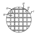
도 3a는 본 발명의 방법에 따른 박막층으로 패터닝된 반도체 웨이퍼의 제2 표면이다.
도 3b는 본 발명의 다른 방버에 따른 2개의 박막층으로 패터닝된 반도체 웨이퍼의 제2 표면이다.Figure 1a is a process flow chart of a preferred setting of the method of the present invention.
1B is a cross section of a semiconductor wafer having a convex warp or bow.
1C is a cross-section of a semiconductor wafer after depositing a thin film layer on a second plane.
FIG. 1D shows a pair of semiconductor wafers processed according to the method of the present invention, fusion bonded, and forming a semiconductor wafer assembly.
2A is a wafer flatness map of a semiconductor wafer having a warp or bow untreated according to the method of the present invention.
FIG. 2B is a wafer flatness map of the semiconductor wafer of FIG. 2A after being processed according to the method of the present invention.
3A is a second surface of a semiconductor wafer patterned with a thin film layer in accordance with the method of the present invention.
3B is a second surface of a semiconductor wafer patterned with two thin films according to another embodiment of the present invention.
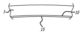
도 1a 내지 1d에 도시된 본 발명의 제1 측면에서, 제1 표면 및 제2 표면(10)을 갖는 반도체 웨이퍼(1)를 제공하는 단계를 포함하는 반도체 웨이퍼의 워프 및/또는 보우를 감소시키는 방법이 개시되며, 반도체 웨이퍼(1)의 표면 프로파일은 도 1b에 나타내어진 바와 같이 워프 및/또는 보우를 포함한다. 보통, 반도체 웨이퍼의 제1 표면은, 회로 또는 다른 전자 또는 전기 장치가 형성되는 반도체 웨이퍼의 표면일 것이나, 이는 본 발명의 제한이 아니며, 일부 경우, 전자 또는 전기 장치는 반도체 웨이퍼의 제2 표면 또는 양쪽 표면에 형성될 수 있다. 워프 및/또는 보우는 반도체 웨이퍼(1)의 표면을 가로질러 측정되며, 보통 반도체 웨이퍼의 볼록한 표면을 가로지르지만 반드시 그런 것은 아니다. 사전에 결정된 두께, 패턴 또는 열팽창계수("CTE")를 갖는 박막층(15)이 제2 표면(10) 상에 증착되어, 반도체 웨이퍼(1)의 제2 표면(10) 상에, 및 반도체 웨이퍼(1)의 제2 표면(10)에 걸쳐 사전에 결정된 변형-변경(strain-modifying), 압축력, 또는 인장력, 또는 압축력 및 인장력을 유도한다. 도 1b 및 1c에 나타내어진 특정 실시예에서, 박막층(15)은 제2 표면(10) 상에 증착되어, 반도체 웨이퍼(1)의 제2 표면(10) 상에, 및 반도체 웨이퍼(1)의 제2 표면(10)에 걸쳐 사전에 결정된 변형-변경 인장력을 유도하고, 이에 의해 일부 위치에서는 약간 높고, 다른 위치에서는 약간 낮은 반도체 웨이퍼 프로파일과 달리, 반도체 웨이퍼는 실질적으로 편평해지지만, 바람직하게는 약간 볼록한 반도체 웨이퍼 프로파일을 남긴다. 박막층(15)은 산화물층, 금속층, 금속 산화물층 또는 세라믹 물질층 또는 균등한 층 물질을 포함할 수 있다. 박막층(15)의 두께, 패턴 또는 CTE는 측정된 워프 및/또는 보우에 기초하여 계산되고 결정될 수 있다. 일 예로서, 박막층(15)은 SiO2 층을 포함할 수 있다. 박막층(15)은 PECVD 공정을 이용하여 증착될 수 있다. 박막층(15)은 약 5 ㎛ 내지 약 8 ㎛의 워프 또는 보우 당 약 1 ㎛의 두께를 가질 수 있다. 반도체 웨이퍼(1)는 사파이어 반도체 웨이퍼, 기판 또는 템플릿 상의 GaN 층을 포함할 수 있다.In a first aspect of the invention as shown in Figs. 1A-1D, there is provided a method of reducing warping and / or bowing of a semiconductor wafer comprising providing a
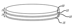
도 1d에 도시된 본 발명의 다른 측면에서, 1개 또는 2개의 반도체 웨이퍼(1)가 본 발명의 방법에 따라 처리된, 한 쌍의 반도체 웨이퍼(1)가 예를 들면, 융합 본딩(fusion bonding) 또는 반도체 웨이퍼 본딩 분야에서 통상의 기술자에게 공지된 균등한 본딩 방법에 의해 서로 본딩되어, 고품질의 본딩된 반도체 웨이퍼 어셈블리를 제공한다. 반도체 웨이퍼는 특정 적층 관계(stacking relationship)에 의해 본딩되는 것으로 나타내어지지만, 일부 적용에서, 본 발명의 적용으로 인한 각각의 반도체 웨이퍼의 더 큰 평탄도가 본딩 품질 및 2개의 반도체 웨이퍼의 상대적 위치의 정확성을 향상시켜, 최종 생성물에서 더 좋은 수율 및 우수한 성능을 제공하기 때문에, 반도체 웨이퍼는 표면 대 표면이 역전될 수 있다.1D, a pair of semiconductor wafers 1, in which one or two
제한이 아닌 예로서, 4-in. 반도체 웨이퍼는 바람직하게 산업-표준 스태퍼 장치(industry-standard stepper equipment)에서의 처리를 위하여 약 80 ㎛ 미만의 워프를 갖는다. 예를 들어, 반도체 웨이퍼가 Canon 스태퍼에 의해 수용될 때, 허용가능한 워프 또는 보우는 반도체 웨이퍼의 표면에 걸쳐 약 40-50 ㎛ 워프 또는 보우인 것이 전형적으로 바람직하다. 40-50 ㎛ 반도체 웨이퍼 워프/보우보다 작은 워프 또는 보우가 특히 후속적인 반도체 웨이퍼 융합 본딩 적용을 위하여 더욱 바람직하다. 임의의 잔류하는 워프/보우는 반도체 웨이퍼의 제1 표면을 가로질러 볼록한 것이 바람직하다. 유사하게, 다른 반도체 웨이퍼와의 본딩을 포함하는 그러한 반도체 웨이퍼의 후속 처리는 높은 수준의 웨이퍼 평탄화를 요구한다. 예를 들어, 직접 융합 본딩 또는 공정 본딩(eutectic bonding)을 이용하는 4-in. 반도체 웨이퍼의 본딩은 전형적으로 반도체 웨이퍼의 표면에 걸쳐 40-50 ㎛ 미만의 워프 또는 보우를 요구할 수 있으며, 전형적으로 반도체 웨이퍼가 편평할수록 본딩 공정에서 감소된 에지 익스클루젼을 얻을 수 있다.By way of example, and not limitation, 4-in. The semiconductor wafers preferably have a warp of less than about 80 [mu] m for processing in industry-standard stepper equipment. For example, when a semiconductor wafer is received by a Canon stepper, it is typically desirable for an acceptable warp or bow to be about 40-50 mu m warp or bow across the surface of the semiconductor wafer. A warp or bow smaller than 40-50 um semiconductor wafer warp / bow is particularly desirable for subsequent semiconductor wafer fusion bonding applications. Any residual warp / bow is preferably convex across the first surface of the semiconductor wafer. Similarly, subsequent processing of such a semiconductor wafer, including bonding with other semiconductor wafers, requires a high level of wafer planarization. For example, 4-in. Using direct fusion bonding or eutectic bonding. Bonding of a semiconductor wafer may typically require a warp or bow of less than 40-50 [mu] m across the surface of the semiconductor wafer, and typically a flattened semiconductor wafer may result in reduced edge excursions in the bonding process.
불행하게도, 사파이어 또는 실리콘 기판 상의 Ⅲ-질화물 반도체 웨이퍼와 같은 통상적인 포토닉 반도체 웨이퍼는 빈번하게 적어도 어느 정도의 워프 및/또는 보우를 갖는 반도체 웨이퍼 표면 프로파일로 제공된다.Unfortunately, conventional photonic semiconductor wafers, such as sapphire or III-nitride semiconductor wafers on silicon substrates, are often provided with a semiconductor wafer surface profile with at least some warp and / or bow.
본 출원인은 본 명세서에서 반도체 웨이퍼 워프 및 보우를 최소화하는 방법을 개시한다. 본 발명의 공정 단계의 바람직한 설정에서, 단계는 반도체 웨이퍼(1)의 제2(비-회로 함유) 표면(10) 상에 사전에 결정된 두께 및 조성을 갖는 이산화규소 또는 "SiO2"(본 명세서에서, "산화물")을 증착시키기 위하여, 플라즈마 증강 화학 기상 증착(PECVD) 툴에 의한 증착 공정을 이용하여 수행된다. 본 발명이 평탄화 박막층(15)으로서 SiO2의 이용에 제한되는 것이 아니라, 이하에 기술된 것과 같은 다른 재료 및 그 균등물이 본 발명에서 평탄화 박막층(15)으로 사용될 수 있음을 명백하게 나타낸다.The Applicant hereby discloses a method for minimizing semiconductor wafer warp and bow. In a preferred set of process steps of the present invention, the method is a semiconductor wafer (1), the second (non-circuit-containing) silicon dioxide or with the surface 10 a in thickness and composition of the predefined "SiO 2" (herein , "Oxide"), using a deposition process by a plasma enhanced chemical vapor deposition (PECVD) tool. It is clear that the present invention is not limited to the use of SiO 2 as the planarization
본 발명의 바람직한 실시예에서, 반도체 웨이퍼(1)의 제2 표면(10) 상에 증착된 산화물 박막층(15)의 원자 간격(atomic spacing)은, Ⅲ-질화물 재료와 같은 포토닉 재료가 증착되는 사파이어와 같은 기판 또는 템플릿의 원자 간격보다 크다. 원자 간격의 차이는 두 가지 재료 사이의 격자 미스매치(lattice mismatch)를 생성하여, 반도체 웨이퍼(1)의 제2 표면 상에 유도된 장력(induced tension)을 초래한다. 결과적으로, 증착된 산화물 박막층(15)은 사파이어 기판 또는 템플릿에 의해 제공되는 것보다 더 큰 표면적을 추구하여, 반도체 웨이퍼의 제2 표면을 확대시키는 경향이 있는 변형(strain)을 생성하고, 산화물 박막층(15)이 제2 표면 영역(10)을 확장하고자 하기 때문에, 이는 사파이어를 평탄화시키는 경향이 있다. 반도체 웨이퍼의 제1 표면은 볼록한 것으로 당연히 가정된다. 따라서, 본 실시예 및 다른 실시예에서, 층(15)은, 층(15)이 증착되기 전 반도체 웨이퍼의 표면에 걸친 워프 또는 보우에 비교하여 반도체 웨이퍼의 제1 표면 및 제2 표면에 걸친 워프 또는 보우을 감소시키는 변형-변경 층(strain-modifying layer)으로 작용한다.In a preferred embodiment of the present invention, the atomic spacing of the oxide
격자 미스매치-관련된 변형에 더하여, 열팽창 미스매치(thermal expansion mismatch)-관련 변형이 반도체 웨이퍼(1) 형태를 변화시키는데 중요한 역할을 하며, 이 현상은 본 발명의 다른 대안적 실시예에서 이용된다. 앞에서 언급한 바와 같이, 유도된 막 응력(induced film stress)에 관련되는 두 가지 기본 메커니즘이 있다: 원자 간격(즉; 격자 미스매치) 및 열팽창계수("CTE") 차이. CTE는 온도에 대한 부피 량(amount volumes) 및 선형 치수의 변화로 생각될 수 있다. CTE는 수학적으로, α = (1/D) (ΔD/ΔT)로 정의되며, 식에서 α는 CTE; D는 부피, 면적 또는 선형 치수; T는 온도이다. 이러한 치수 변화는 재료마다 다르지만, 보통 가열될 때 재료가 팽창한다.In addition to the lattice mismatch-related variations, thermal expansion mismatch-related strain plays an important role in changing the shape of the
CTE 자체는 물리적 현상이며, 바람직한 실시예에서, 특히, 특정 박막층(15) 재료가 실온이 아닌 온도에서 반도체 웨이퍼(1) 표면 상에 증착되는 경우, 반도체 웨이퍼 평탄화 방법으로서 이용된다. CTE는, 온도가 증가함에 따라 재료의 높은 수준의 양자 상태가 비대칭 전위 우물에서 더 많이 채워진다는 사실에 기인하여 발생한다. 이 높은 수준의 양자 상태는 평형 반경보다 큰 값에서 증가하는 확률 밀도를 갖는다. 다시 말하면, 시간 평균적으로, 원자들은 온도가 증가함에 따라 서로 더 멀리 떨어져서 더 많은 시간을 보낸다. 두 가지 재료 사이에 CTE 미스매치가 있는 경우, 온도에 따른 평균 원자 간격 변화량은 각각의 재료에 있어서 다르다. CTE 막 응력의 기본적인 예(격자 미스매치 무시)는, 호스트 기판보다 더 큰 CTE를 갖는 막이 높은 온도(elevated temperature)에서 증착되는 경우이다. 증착 온도에서, 구조는 응력 중립적(stress-neutral)이지만, 구조가 냉각되면, 박막층(15)은 기판보다 더 수축되어, 박막층(15)이 제2 표면(10)에 걸쳐 인장 응력 또는 압축 응력(막 재료의 CTE에 의존함)을 갖게 된다.The CTE itself is a physical phenomenon and is used as a semiconductor wafer planarization method in the preferred embodiment, particularly when the specific
본 발명의 산화물 증착을 위한 공정 단계의 바람직한 설정은 표 1에 나타내어진 바와 같은 하기 파라미터를 포함할 수 있다.Preferred settings of process steps for the oxide deposition of the present invention may include the following parameters as shown in Table 1:
또는
100% SiH4 흐름: 약 0.5 내지 50 sccm - 95% N 2/5% SiH 4 flow: about 10 to 2000 sccm
or
100% SiH 4 flow: about 0.5 to 50 sccm
증착된 산화물 박막층(15)은 바람직하게 약 10% 미만의 비균일성(non-uniformity)을 갖는다. 약 300℃ 내지 400℃ 범위 내에서 증착된 산화물 박막층(15)이 허용가능한 압축 효과(compressive effect)를 나타내는 것으로 관찰되어기 때문에, 산화물 박막층(15) 증착 중 공정 온도는 실질적인 공정 제약이 아니다.The deposited oxide
상기 예시적인 공정 파라미터를 이용하여, 본 발명의 바람직한 실시예는 증착된 산화물 박막층(15) 1 ㎛ 당 대략적으로 약 5-8 ㎛의 워프 또는 보우 완화(relef)를 초래한다.Using the above exemplary process parameters, a preferred embodiment of the present invention results in a warp or bow relef (roughly) of about 5-8 [mu] m per 1 [mu] m of deposited oxide
도 2a 및 2b를 참조하면, Sigmatech 배압 반도체 웨이퍼 형태 측정 장치를 이용하여 수행된 반도체 웨이퍼 계측 측정으로부터의 워프 및 보우 조정 데이터의 그래픽 묘사가 나타내어지며, 비처리된 반도체 웨이퍼(도 2a)로부터 본 발명의 방법에 따라 처리된 동일한 반도체 웨이퍼(도 2b)의 평탄도 향상을 보여준다. 이들 도면의 범례에서 더 낮은 범위의 측정에서 이 평탄도 향상이 나타내어진다.Referring to Figures 2a and 2b, a graphical depiction of warp and bow adjustment data from semiconductor wafer metrology measurements performed using a Sigmatech back pressure semiconductor wafer morphology measurement device is shown, (Fig. 2B) treated according to the method of Fig. In the legend of these figures, this flatness improvement is shown in the lower range measurements.
본 발명의 바람직한 실시예의 실험적 실시는 본 발명의 방법에 따라 처리된 4in. 반도체 웨이퍼(1) 상에 증착된 1 ㎛의 산화물 박막층(15)에 대하여 약 6.3 ㎛의 평균 워프 감소를 가져왔고, 증착된 1 ㎛ 산화물에 대하여 약 3.4 ㎛의 평균 보우 감소가 있었다.Experimental implementation of the preferred embodiment of the present invention is based on the 4in. Resulting in an average warp reduction of about 6.3 [mu] m for the 1 [mu] m
총 두께 변화(Total thickness variation) 또는 "TTV"는 증착된 산화물 박막층(15)의 비균일성에 의해 대략 증가 또는 감소할 수 있으며, 그러한 반도체 웨이퍼(1) 두께는 목표 증착 산화물 두께의 약 80-90%에서 조절된다.The total thickness variation or "TTV" can be substantially increased or decreased by the non-uniformity of the deposited oxide
본 발명의 단계를 이용하는 샘플 반도체 웨이퍼 처리(processing run)에서, 목표 2 ㎛ 산화물 박막층(15) 증착 후에, 반도체 웨이퍼 워프가 56.5 ㎛로부터 43.3 ㎛로 감소된 것으로 나타났고; 보우는 29.2 ㎛로부터 22.7 ㎛로 감소된 것으로 나타났으며; TTV는 6.8 ㎛로부터 7.4 ㎛로 증가한 것으로 나타났고; 반도체 웨이퍼 두께는 662.9 ㎛로부터 664.7 ㎛로 증가한 것으로 나타났다. 다른 예시적인 워프 감소 데이터는 하기 표 2에 나타내어진다.In a sample semiconductor wafer processing run using the steps of the present invention, after deposition of the target 2 탆
제2 표면 워프 및 보우 조정 산화물 박막층(second surface warp and bow adjustment oxide thin film layer)(15)이 증착되면, 워프 및 보우 조정 산화물 박막층(15) 증착 단계가 반복되지 않는 한, 반도체 웨이퍼(1)는 BOE 및 HF에 노출되지 않는다.When a second surface warp and bow adjustment oxide
또한, 증착된 박막층(15) 산화물 두께 균일성은 예를 들면, 레이저 리프트오프(LLO) 균일성과 같은 후속 공정 단계 균일성에 일부 영향을 미칠 수 있다. LLO 균일성은 산화물 박막층(15) 균일성에 의해서 야기되는 UV 레이저 광의 4분의 1 파장 간섭 조건(quarter-wavelength interference condition)에 의해 영향을 받고, 층(15)의 UV 흡수에 의한 영향을 받지 않을 수 있다.In addition, the deposited
본 발명의 방법이, 제한의 방식이 아닌 예를 들어, 설명 및 논의 목적을 위하여 이용된, c-평면 사파이어 상에 증착된 예시적 바람직한 압축 PECVD 산화물 박막층(15)만을 이용하여 실시될 필요가 없음을 명백하게 나타낸다. 본 발명의 방법 및 청구범위는 반도체 웨이퍼(1)의 형태, 워프 및 보우를 조작하도록 임의의 반도체 웨이퍼(1)의 임의의 표면 상에 증착된 임의의 고응력 박막층(15)의 이용을 명시적으로 포함한다. 따라서, 증착된 박막층(15)은 이산화규소 재료에 제한되지 않으며; 제2 표면(10) 상에서의 격자 미스매치 또는 상이한 CTEs에 기인하여 사전에 결정된 압축력, 인장력, 또는 압축력 및 인장력을 유도하는데 충분한 미리 결정 두께로 반도체 웨이퍼(1) 표면 상에 증착될 수 있는 임의의 적합한 박막층(15)이 이용될 수 있다The method of the present invention need not be performed using only the exemplary preferred compacted PECVD oxide
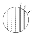
대안적인 방법이 도 3a 및 3b에 나타내어진다. 도 3a에서, 박막층(15)이 반도체 웨이퍼(1)의 인접한 표면(10) 상에 압축력 또는 인장력을 나타내도록 선택되는지 여부에 관계없이, 박막층(15)은 긴 스트립(strip)을 형성하도록 패터닝되며, 이는 변형 변경 효과(strain-modifying effect)를 위한 지배적인 축을 제공한다. 이는, 보우 또는 워프가 대략 단일 축이거나 대부분 대략 단일 축인 경우에 유용할 수 있다. 그러나, 보우 또는 워프가 대략 2개의 축이고 동일하지 않은 경우, 도 3b에 도시된 바와 같이, 제2 패터닝된 박막층(15)이 증착되어 제2 축을 중심으로 배향될 수 있다. 도 3a에서 단순히 층(15)의 스트립의 폭을 선택함으로써 동일하지 않은 변형이 얻어질 수도 있음을 주목한다. 또한, 도 3b에서, 수직 및 수평 스트립은 동일하거나 상이한 박막층 재료로 이루어질 수 있다. 이와 관련하여, 일부 경우, 보우 또는 워프는 2개 축을 중심으로 반대 방향으로 있을 수 있으며, 이 경우 상이한 박막층 재료가 이용되어, 하나는 인접한 반도체 기판 상에 압축력을 유도하고, 다른 하나는 인접한 기판 상에 인장력을 유도할 수 있다.An alternative method is shown in Figures 3a and 3b. 3A, the
다른 조성을 가져 충분한 반도체 웨이퍼 표면 변형을 부여하여 반도체 웨이퍼(1) 표면 프로파일을 변화시키는, 반도체 웨이퍼(1) 표면 상에 증착될 수 있는 다수의 적합한 박막층(15) 재료가 상업적으로 이용가능하다. 실리콘 산화물은 반도체 웨이퍼(1) 상에 증착하기 간단하고, 반도체 웨이퍼(1)의 보우 및 워프를 변형시키는 응력 상태에서 성장할 수 있기 때문에 그러한 적용을 위하여 매우 적합하나, 대안적인 실시예에서, 실리콘 질화물, 세라믹, 금속 또는 금속 산화물 박막층(15)이 이용될 수 있으며, 본 발명의 방법의 범위 내에서 고려된다. 또한, 상기 언급된 반도체 웨이퍼(1)는 일반적인 형상을 갖는 것으로 간주될 수 있으며, 본 발명의 방법은 반도체 웨이퍼(1)의 제2 표면(1) 상에 변형-변경 또는 압축-변형(compression-modifying) 박막층(15)을 증착함으로써 임의의 일반적인 기판 형상을 평탄화시키는 기능을 한다. 따라서, 박막층에 대한 주요 변수는, 일부 경우 동일한 재료에 대하여 대상이 되는 상이한 막 두께에 따라 다를 수 있는, 재료의 특성인 열팽창계수와 함께, 재료, 두께 및 박막층 패턴이다.A number of suitable thin film layer (15) materials are commercially available that can be deposited on the surface of a semiconductor wafer (1) that has different composition and imparts sufficient semiconductor wafer surface deformation to change the surface profile of the semiconductor wafer (1). Silicon oxide is very suitable for such applications because it is simple to deposit on the
전술한 c-평면 GaN-온-사파이어의 바람직한 실시예에서, 에피택셜 표면 위로 볼 때, 반도체 웨이퍼(1)는 종종 상당히 균일하게 볼록해지는 경향이 있으며, 즉, 가장 높은 지점이 GaN 표면의 중심을 향한다. 이와 같은 경우, 반도체 웨이퍼(1)의 제2 표면(10) 상에 블랭킷 압축 산화물 박막층(blanket compressive oxide thin film layer)(15)을 전술한 바와 같이 증착하는 것이 특히 효과적이다. 그러나, 증착된 박막층(15)은 SiO2 재료에 제한될 필요가 없고, 증착된 박막층 재료는 GaN 또는 반도체 웨이퍼 재료와 비교하여 반도체 웨이퍼(1)에 반대 곡률(curvature)을 부여하는 임의의 재료일 수 있다.In the preferred embodiment of the above-described c-plane GaN-on-sapphire, when viewed over the epitaxial surface, the
반도체 웨이퍼(1)가 오목한 경우에, 전술한 복록한 비평면 상태와 같이 반도체 웨이퍼의 제2 표면에 압축 박막층(15)을 적용하는 것보다, 사파이어에 인장 응력을 부여하는 증착된 박막층(15)이 적용될 수 있다. GaN 자체는 본 발명의 이 실시예에 대한 적합한 후보이다.The deposited
m-평면 사파이어 상에서 성장한 반극성 GaN과 같이 상이한 결정학적 방향에서 상이한 곡률을 갖는 반도체 웨이퍼(1)의 일반적 경우에, 본 발명은 하나의 축을 따라 보우를 감소시키지만, 수직 방향으로 이를 증가시킬 수 있다.In the general case of a
이러한 우려를 해결하기 위하여, 반도체 분야에 공지된 "쉐도우 마스크(shadow mask)"가 반도체 웨이퍼(1)의 제2 표면(10)의 상이한 부분 또는 영역 상에 사전에 결정된 변형-변경 또는 인장 특성을 갖는 변형-변경 박막층(15)을 선택적으로 증착시키는데 이용될 수 있는 대안적인 실시예가 개시된다.In order to overcome this concern, a "shadow mask" as known in the semiconductor arts can be used to impart predetermined deformation-altering or tensile properties on different parts or regions of the
반도체 웨이퍼(1)의 제2 표면(10)에 블랭킷 평탄화(blanket planarizing) 박막층(15)을 증착하고, 도 4에 나타내어진 예시적 패턴과 같이 사전에 결정된 박막층(15) 패턴으로 포토리소그래피를 이용하여 반도체 웨이퍼(1)를 패터닝하고, 이어서 평탄화 박막층(15)의 사전에 결정된 영역 또는 부분을 선택적으로 제거하여, 웨이퍼 평탄도의 원하는 변화를 유도함으로써, 동등한 효과가 얻어질 수 있다.A blanket planarizing
제한되지 않는 예로, 사전에 결정된 변형-변경 패턴을 갖는 쉐도우 마스크를 이용함으로써, 사용자는 상이한 축을 따라 형상을 상이하게 변형시키기 위하여, 예를 들어 반도체 웨이퍼 영역의 2/3로 이루어진 스트립으로서 압축 박막층(15) 산화물을 증착할 수 있으며, 반도체 웨이퍼(1)의 중앙 1/3 상에 인장 질화물을 증착시킬 수 있다(도 3a 및 3b).By way of example, and not by way of limitation, by using a shadow mask with a predetermined deformation-change pattern, the user can use a compression thin-film layer (e.g., a strip formed of 2/3 of the semiconductor wafer area) 15) oxide and can deposit tensile nitride on the mid-third of the semiconductor wafer 1 (Figs. 3a and 3b).
상이한 또는 변화하는 압축/인장 층 패턴은, 특정 반도체 웨이퍼 보우에 대하여 최적 변경 박막층 또는 층들(15) 조합 패턴을 모델링하기 위하여, 주어진 반도체 웨이퍼 형성에 기초하여 예를 들어, 변형 모델링 소프트웨어를 이용하여 결정될 수 있다.Different or varying compression / stretch layer patterns may be determined using, for example, strain modeling software based on a given semiconductor wafer formation, to model the optimal change thin film layer or layers 15 combination pattern for a particular semiconductor wafer bow .
많은 변화 및 변경이 본 발명의 방법의 사상 및 범위로부터 벗어나지 않고 통상의 기술자에 의해 이루어질 수 있다. 따라서, 설명된 실시예는 예시적 목적으로서 기재된 것이며, 본 출원에 대한 우선권을 주장하는 임의의 후속 출원의 청구범위에 의해 정의되는 바와 같은, 본 발명을 제한하고자 받아들여져서는 안되는 것을 이해하여야 한다.Many changes and modifications may be made by one of ordinary skill in the art without departing from the spirit and scope of the method of the present invention. Accordingly, it is to be understood that the described embodiments are set forth for purposes of illustration and are not to be construed as limiting the invention, as defined by the claims of any subsequent application claiming priority to this application.
예를 들어, 그러한 청구범위의 요소가 특정 조합으로 기재될 수 있다는 사실에도 불구하고, 본 발명은, 그러한 조합에서 처음에 청구되지 않았을 때에도 상기에서 개시된, 더 적은, 더 많은 또는 상이한 요소의 다른 조합을 포함한다.For example, despite the fact that elements of such claims may be described in a particular combination, the invention also encompasses other combinations of the lesser, more or different elements described above, even when not initially claimed in such combinations .
본 발명 및 다양한 실시예를 기술하기 위하여 본 명세서에 이용되는 단어는 일반적으로 정의되는 의미로 이해될 뿐 아니라, 본 명세서에 특별히 정의된 것에 의해, 통상적으로 정의된 의미를 벗어난 구조, 재료 또는 활동을 포함한다. 따라서, 요소가 하나 이상의 의미를 포함하는 것으로 본 명세서의 문맥에서 이해될 수 있는 경우, 후속 청구범위에서 그 이용은 명세서 및 단어 그 자체에 의해 뒷받침되는 모든 가능한 의미에 대해 포괄적인 것으로 이해되어야 한다.It is to be understood that the words used herein to describe the present invention and various embodiments are not to be understood as being in a generally defined sense but also to include structures, materials, or activities that are outside of the commonly defined meanings by those specifically defined herein . Accordingly, where an element may be understood in the context of this specification as including one or more meanings, its use in the following claims is to be understood as being inclusive of all possible meanings supported by the specification and the words themselves.
그러므로, 본 출원에 대한 우선권을 주장하는 임의의 후속 출원에서 임의의 청구범위의 단어 또는 요소의 정의는, 문자 그대로 기재된 요소의 조합뿐 아니라, 실질적으로 동일한 결과를 얻기 위하여 실질적으로 동일한 방식으로 실질적으로 동일한 기능을 수행하기 위한 모든 균등한 구조, 재료 또는 활동을 포함하는 것으로 정의되어야 한다. 이러한 의미에서, 2개 이상의 요소의 균등 치환이 이하의 청구범위에서 임의의 하나에 대하여 이루어질 수 있거나, 또는 단일 요소가 그러한 청구범위에서2개 이상의 요소로 치환될 수 있는 것으로 고려된다.Therefore, the definition of a word or element in any claim in any subsequent application claiming priority from the instant application is intended to encompass not only the combination of elements literally described, but also substantially all of the elements in a substantially similar manner But should be defined as including all equivalent structures, materials, or activities for performing the same function. In this sense, it is contemplated that equivalent permutation of two or more elements may be made to any one of the following claims, or that a single element may be substituted for more than one element in such claim.
요소들이 특정 조합으로 작용하고 그와 같이 청구되는 것으로 상기에서 기술될 수 있으나, 청구된 조합으로부터 일 이상의 요소가 일부 경우 조합으로부터 배제될 수 있으며, 그러한 청구된 조합이 서브컴비네이션 또는 서브컴비네이션의 변이에 관한 것일 수 있음을 명백하게 이해하여야 한다.Although elements may be described above as acting in a certain combination and claimed as such, it is to be understood that more than one element from the claimed combination may in some cases be excluded from the combination, and such claimed combination may be used in variations of the subcombination or subcombinations But it should be understood clearly that the
당해 기술분야에서 통상의 지식을 가진 자에 의해 관찰될 때, 현재 공지되어 있거나 또는 후에 고안되는, 임의의 후속적으로 청구되는 요지로부터의 대단찮은 변화는 그러한 청구범위의 범위 내에 균등한 것으로 명백하게 고려된다. 따라서, 당해 기술분야의 통상의 기술자에게 현재 또는 추후 공지되는 자명한 치환은 정의된 요소의 범위 내인 것으로 정의된다.When viewed by one of ordinary skill in the art, great changes from any subsequently claimed subject matter, now known or later devised, are expressly contemplated as being within the scope of such claims do. Accordingly, obvious substitutions presently or hereinafter known to those of ordinary skill in the art are defined as within the scope of the defined elements.
본 출원에 대하여 우선권을 주장하는 임의의 후속 출원의 임의의 청구범위는 상기에서 구체적으로 예시되고, 설명된 것, 개념적으로 균등한 것, 자명하게 치환될 수 있는 것 및 본 발명의 본질적인 사상을 본질적으로 포함하는 것을 포함하는 것으로 이해되어야 한다.Any claim of any subsequent application claiming priority to this application is to be construed as being particularly illustrative of the foregoing, of conceptual equivalence, of being able to be expressly replaced, and of essentially intrinsic thought of the invention And the like.
Claims (22)
반도체 웨이퍼의 표면을 가로질러 상기 워프 또는 보우를 측정하는 단계; 및
상기 제2 표면 상에 사전에 결정된 두께를 갖는 산화물층을 증착시켜, 상기 제2 표면 상에 사전에 결정된 압축력, 인장력, 또는 압축력 및 인장력의 조합을 유도함으로써, 상기 산화물층이 증착되기 전 상기 반도체 웨이퍼 표면 프로파일의 워프 또는 보우와 비교하여, 반도체 웨이퍼 표면 프로파일의 워프 또는 보우를 감소시키는 단계를 포함하는
반도체 웨이퍼에서 워프 또는 보우를 감소시키는 방법.
Providing a semiconductor wafer having a first surface and a second surface, wherein the semiconductor wafer surface profile comprises a warp or bow;
Measuring the warp or bow across the surface of the semiconductor wafer; And
Depositing an oxide layer having a predetermined thickness on the second surface to induce a predetermined compressive force, tensile force, or a combination of compressive and tensile forces on the second surface, Reducing the warp or bow of the semiconductor wafer surface profile, as compared to a warp or bow of the wafer surface profile
A method for reducing warp or bow on a semiconductor wafer.
상기 산화물층 두께는 상기 반도체 웨이퍼 표면 프로파일에서 측정된 워프 또는 보우에 기초하여 사전에 결정되는
방법.
The method according to claim 1,
The oxide layer thickness is determined in advance based on the warp or bow measured in the semiconductor wafer surface profile
Way.
상기 산화물층은 SiO2 층인
방법.
The method according to claim 1,
The oxide layer is a SiO 2 layer
Way.
상기 산화물층은 PECVD 공정에서 증착되는
방법.
The method according to claim 1,
The oxide layer is deposited in a PECVD process
Way.
상기 산화물층은 5 ㎛ 내지 8 ㎛의 워프 또는 보우 당 1 ㎛의 두께를 갖는
방법.
The method according to claim 1,
The oxide layer has a thickness of 1 占 퐉 per warp or bow of 5 占 퐉 to 8 占 퐉
Way.
상기 반도체 웨이퍼는 사파이어 웨이퍼, 기판 또는 템플릿 상의 GaN인
방법.
The method according to claim 1,
The semiconductor wafer may be a sapphire wafer, a substrate or a GaN
Way.
상기 반도체 웨이퍼의 표면을 가로질러 상기 워프 또는 보우를 측정하는 단계; 및
상기 제2 표면 상에 사전에 결정된 두께를 갖는 적어도 하나의 변형-변경 층(strain-modifying layer)을 증착하여, 상기 제2 표면 상에 사전에 결정된 압축력, 인장력, 또는 압축력 및 인장력을 유도함으로써, 상기 적어도 하나의 변형-변경 층이 증착되기 전 상기 반도체 웨이퍼의 표면의 워프 또는 보우와 비교하여, 상기 적어도 하나의 변형-변경 층이 상기 반도체 웨이퍼의 표면의 워프 또는 보우를 감소시키는 단계를 포함하는
반도체 웨이퍼에서 워프 또는 보우를 감소시키는 방법.
Providing a semiconductor wafer having a first surface and a second surface, wherein the semiconductor wafer surface profile comprises a warp or bow;
Measuring the warp or bow across the surface of the semiconductor wafer; And
By depositing at least one strain-modifying layer having a predetermined thickness on the second surface to induce a predetermined compressive force, tensile force, or compressive force and tensile force on the second surface, Wherein said at least one strain-altering layer reduces warping or bowing of the surface of said semiconductor wafer as compared to a warp or bow of the surface of said semiconductor wafer before said at least one strain-altering layer is deposited
A method for reducing warp or bow on a semiconductor wafer.
상기 산화물층 두께는 측정된 워프 또는 보우에 적어도 부분적으로 기초하여 결정되는
방법.
8. The method of claim 7,
The oxide layer thickness is determined based at least in part on the measured warp or bow
Way.
상기 적어도 하나의 변형-변경 층은 실리콘 질화물 층인
방법.
8. The method of claim 7,
Wherein the at least one strain-altering layer is a silicon nitride layer
Way.
상기 적어도 하나의 변형-변경 층은 금속 산화물 재료인
방법.
8. The method of claim 7,
Wherein the at least one strain-altering layer is a metal oxide material
Way.
상기 적어도 하나의 변형-변경 층 Ⅲ족-질화물인
방법.
8. The method of claim 7,
The at least one strain-altering layer III-nitride
Way.
상기 적어도 하나의 변형-변경 층은 PECVD 공정에서 증착되는
방법.
8. The method of claim 7,
The at least one strain-altering layer is deposited in a PECVD process
Way.
상기 적어도 하나의 변형-변경 층은 물리 기상 증착 공정에서 증착되는
방법.
8. The method of claim 7,
The at least one strain-altering layer is deposited in a physical vapor deposition process
Way.
상기 적어도 하나의 변형-변경 층은 각각 약 5 ㎛ 내지 8 ㎛의 워프 또는 보우 당 1 ㎛의 두께를 갖는
방법.
8. The method of claim 7,
Wherein the at least one strain-altering layer has a thickness of about 1 占 퐉 per warp or bow of about 5 占 퐉 to about 8 占 퐉,
Way.
상기 적어도 하나의 변형-변경 층은 패터닝되는
방법.
8. The method of claim 7,
The at least one strain-altering layer is patterned
Way.
상기 반도체 웨이퍼를, 제7항의 방법으로 처리된 일 이상의 다른 반도체 웨이퍼에 융합 본딩(fusion bonding)시키는 단계를 더 포함하는
방법.
8. The method of claim 7,
Further comprising the step of fusion bonding the semiconductor wafer to one or more other semiconductor wafers processed by the method of claim 7,
Way.
상기 제2 표면 상의 적어도 하나의 변형-변경 층을 포함하며,
상기 적어도 하나의 변형-변경 층은 상기 제2 표면 상에 압축력, 인장력, 또는 압축력 및 인장력을 유도하여, 상기 적어도 하나의 변형-변경 층이 적용되기 전 상기 반도체 웨이퍼의 워프 또는 보우 아래로, 상기 반도체 웨이퍼의 워프 또는 보우를 감소시키는
반도체 웨이퍼.
A semiconductor wafer having a first surface and a second surface; And
And at least one strain-altering layer on the second surface,
Wherein the at least one deformation-altering layer induces compressive, tensile, or compressive and tensile forces on the second surface such that the at least one deformation-modifying layer is under a warp or bow of the semiconductor wafer before the at least one deformation- Reducing the warp or bow of a semiconductor wafer
Semiconductor wafer.
상기 적어도 하나의 변형-변경 층은 제1 변형-변경 층 및 제2 변형-변경 층을 포함하는
반도체 웨이퍼.
18. The method of claim 17,
Wherein the at least one strain-altering layer comprises a first strain-altering layer and a second strain-
Semiconductor wafer.
상기 제1 변형-변경 층은 상기 반도체 웨이퍼 상에서 제1 방향으로 연장하는 복수의 연장된 층 세그먼트(elongated layer segments)를 형성하도록 패터닝되고, 상기 제2 변형-변경 층은 상기 반도체 웨이퍼 상에서 제2 방향으로 연장하는 복수의 연장된 층 세그먼트를 형성하도록 패터닝되는
반도체 웨이퍼.
19. The method of claim 18,
Wherein the first strain-altering layer is patterned to form a plurality of elongated layer segments extending in a first direction on the semiconductor wafer, and the second strain-altering layer is patterned on the semiconductor wafer in a second direction To form a plurality of extended layer segments extending < RTI ID = 0.0 >
Semiconductor wafer.
하나의 변형-변경 층은 상기 제2 표면 상에 압축력을 가하고, 상기 제2 변형-변경 층은 상기 제2 표면 상에 인장력을 가하는
반도체 웨이퍼.
20. The method of claim 19,
Wherein one deformation-modifying layer applies a compressive force on the second surface, and the second deformation-modifying layer applies a tensile force on the second surface
Semiconductor wafer.
상기 적어도 하나의 변형-변경 층은 SiO2, 실리콘 질화물, 금속 산화물 재료 또는 Ⅲ족-질화물로 이루어진 군으로부터 선택되는
반도체 웨이퍼.
18. The method of claim 17,
The at least one strain-change layer is SiO 2, silicon nitride, metal oxide material or Ⅲ group - selected from the group consisting of nitride
Semiconductor wafer.
상기 반도체 웨이퍼는 사파이어 웨이퍼, 기판 또는 템플릿 상의 GaN이며, 상기 변형-변경 층은 SiO2 층인
반도체 웨이퍼.18. The method of claim 17,
Wherein the semiconductor wafer is a sapphire wafer, a substrate or GaN on a template, the deformation-modifying layer being a SiO 2 layer
Semiconductor wafer.
Applications Claiming Priority (5)
| Application Number | Priority Date | Filing Date | Title |
|---|---|---|---|
| US201562268262P | 2015-12-16 | 2015-12-16 | |
| US62/268,262 | 2015-12-16 | ||
| US15/379,759 US9978582B2 (en) | 2015-12-16 | 2016-12-15 | Methods for improving wafer planarity and bonded wafer assemblies made from the methods |
| US15/379,759 | 2016-12-15 | ||
| PCT/US2016/067379 WO2017106788A1 (en) | 2015-12-16 | 2016-12-16 | Methods for improving wafer planarity and bonded wafer assemblies made from the methods |
Publications (1)
| Publication Number | Publication Date |
|---|---|
| KR20180095609A true KR20180095609A (en) | 2018-08-27 |
Family
ID=59057725
Family Applications (1)
| Application Number | Title | Priority Date | Filing Date |
|---|---|---|---|
| KR1020187020189A KR20180095609A (en) | 2015-12-16 | 2016-12-16 | Method for improving wafer flatness and bonded wafer assembly made from the method |
Country Status (6)
| Country | Link |
|---|---|
| US (1) | US9978582B2 (en) |
| JP (2) | JP6952697B2 (en) |
| KR (1) | KR20180095609A (en) |
| CN (1) | CN108604572A (en) |
| TW (1) | TWI765874B (en) |
| WO (1) | WO2017106788A1 (en) |
Cited By (1)
| Publication number | Priority date | Publication date | Assignee | Title |
|---|---|---|---|---|
| KR20210053350A (en) * | 2018-09-28 | 2021-05-11 | 램 리써치 코포레이션 | Asymmetric Wafer Bow Compensation |
Families Citing this family (15)
| Publication number | Priority date | Publication date | Assignee | Title |
|---|---|---|---|---|
| WO2015084851A1 (en) * | 2013-12-04 | 2015-06-11 | 3M Innovative Properties Company | Flexible light emitting semiconductor device with large area conduit |
| US10847419B2 (en) * | 2018-03-14 | 2020-11-24 | Raytheon Company | Stress compensation and relief in bonded wafers |
| CN108649021A (en) * | 2018-07-19 | 2018-10-12 | 长江存储科技有限责任公司 | Silicon wafer warpage adjusts structure and forming method thereof |
| CN109155235A (en) * | 2018-08-16 | 2019-01-04 | 长江存储科技有限责任公司 | It is controlled using the wafer flatness of back side collocation structure |
| JP2020047617A (en) * | 2018-09-14 | 2020-03-26 | キオクシア株式会社 | Substrate processing device, method of manufacturing semiconductor device, and processed substrate |
| US10896821B2 (en) * | 2018-09-28 | 2021-01-19 | Lam Research Corporation | Asymmetric wafer bow compensation by physical vapor deposition |
| JP2020161685A (en) * | 2019-03-27 | 2020-10-01 | 東京エレクトロン株式会社 | Deposition device and deposition method |
| JP7259527B2 (en) * | 2019-04-26 | 2023-04-18 | 富士電機株式会社 | Semiconductor substrate manufacturing method and semiconductor device manufacturing method |
| US10790296B1 (en) * | 2019-05-21 | 2020-09-29 | Sandisk Technologies Llc | Distortion-compensated wafer bonding method and apparatus using a temperature-controlled backside thermal expansion layer |
| KR20210044654A (en) * | 2019-10-15 | 2021-04-23 | 에스케이하이닉스 주식회사 | wafer supporting structure |
| CN111048429B (en) * | 2019-12-23 | 2022-05-27 | 武汉新芯集成电路制造有限公司 | Wafer bonding method |
| FR3121548B1 (en) * | 2021-03-30 | 2024-02-16 | Soitec Silicon On Insulator | METHOD FOR PREPARING AN ADVANCED SUBSTRATE, PARTICULARLY FOR PHOTONIC APPLICATIONS |
| WO2023272614A1 (en) | 2021-06-30 | 2023-01-05 | Yangtze Memory Technologies Co., Ltd. | Three-dimensional memory devices and methods for forming the same |
| CN113906542A (en) * | 2021-08-30 | 2022-01-07 | 长江存储科技有限责任公司 | Wafer stress control using backside film deposition and laser annealing |
| US20240105641A1 (en) * | 2022-09-28 | 2024-03-28 | Applied Materials, Inc. | Correction of global curvature during stress management |
Family Cites Families (22)
| Publication number | Priority date | Publication date | Assignee | Title |
|---|---|---|---|---|
| US4790920A (en) | 1985-12-20 | 1988-12-13 | Intel Corporation | Method for depositing an al2 O3 cap layer on an integrated circuit substrate |
| US4830984A (en) * | 1987-08-19 | 1989-05-16 | Texas Instruments Incorporated | Method for heteroepitaxial growth using tensioning layer on rear substrate surface |
| JPH01256126A (en) * | 1988-04-06 | 1989-10-12 | Sumitomo Electric Ind Ltd | Manufacture of semiconductor device |
| US5286671A (en) | 1993-05-07 | 1994-02-15 | Kulite Semiconductor Products, Inc. | Fusion bonding technique for use in fabricating semiconductor devices |
| JPH08111409A (en) * | 1994-10-12 | 1996-04-30 | Rohm Co Ltd | Manufacturing for semiconductor device |
| JPH08227834A (en) * | 1995-02-21 | 1996-09-03 | Sony Corp | Semiconductor wafer and manufacture thereof |
| EP1097782B1 (en) | 1999-01-20 | 2006-11-15 | Shin-Etsu Handotai Co., Ltd | Wire saw and cutting method |
| US7169685B2 (en) * | 2002-02-25 | 2007-01-30 | Micron Technology, Inc. | Wafer back side coating to balance stress from passivation layer on front of wafer and be used as die attach adhesive |
| US20070194342A1 (en) | 2006-01-12 | 2007-08-23 | Kinzer Daniel M | GaN SEMICONDUCTOR DEVICE AND PROCESS EMPLOYING GaN ON THIN SAPHIRE LAYER ON POLYCRYSTALLINE SILICON CARBIDE |
| US7880278B2 (en) * | 2006-05-16 | 2011-02-01 | Taiwan Semiconductor Manufacturing Company, Ltd. | Integrated circuit having stress tuning layer |
| US8557681B2 (en) * | 2006-10-30 | 2013-10-15 | International Rectifier Corporation | III-nitride wafer fabrication |
| US8664747B2 (en) | 2008-04-28 | 2014-03-04 | Toshiba Techno Center Inc. | Trenched substrate for crystal growth and wafer bonding |
| US20100314725A1 (en) * | 2009-06-12 | 2010-12-16 | Qualcomm Incorporated | Stress Balance Layer on Semiconductor Wafer Backside |
| WO2012043616A1 (en) * | 2010-09-28 | 2012-04-05 | 株式会社村田製作所 | Piezoelectric device and method for manufacturing piezoelectric device |
| WO2012043615A1 (en) * | 2010-09-28 | 2012-04-05 | 株式会社村田製作所 | Method for manufacturing piezoelectric device |
| EP2622630A1 (en) * | 2010-09-30 | 2013-08-07 | Freescale Semiconductor, Inc. | Methods for processing a semiconductor wafer, a semiconductor wafer and a semiconductor device |
| JP5642628B2 (en) * | 2011-05-27 | 2014-12-17 | 東京エレクトロン株式会社 | Substrate warp removal apparatus, substrate warp removal method, and storage medium |
| JP5418564B2 (en) * | 2011-09-29 | 2014-02-19 | 信越半導体株式会社 | Method for calculating warpage of bonded SOI wafer, and method for manufacturing bonded SOI wafer |
| US8900969B2 (en) * | 2012-01-27 | 2014-12-02 | Skyworks Solutions, Inc. | Methods of stress balancing in gallium arsenide wafer processing |
| KR20140104062A (en) * | 2013-02-15 | 2014-08-28 | 삼성전자주식회사 | A method of producing a p-type nitride semiconductor and a method of manufacturing a nitride semiconductor light emitting device by using the same |
| US9184041B2 (en) * | 2013-06-25 | 2015-11-10 | Taiwan Semiconductor Manufacturing Co., Ltd. | Integrated circuit with backside structures to reduce substrate warp |
| CN105448762A (en) * | 2014-08-28 | 2016-03-30 | 中国科学院微电子研究所 | Method for adjusting warping degree of substrate |
-
2016
- 2016-12-15 US US15/379,759 patent/US9978582B2/en active Active
- 2016-12-16 TW TW105141940A patent/TWI765874B/en not_active IP Right Cessation
- 2016-12-16 CN CN201680081960.2A patent/CN108604572A/en active Pending
- 2016-12-16 KR KR1020187020189A patent/KR20180095609A/en not_active Application Discontinuation
- 2016-12-16 JP JP2018531326A patent/JP6952697B2/en active Active
- 2016-12-16 WO PCT/US2016/067379 patent/WO2017106788A1/en active Application Filing
-
2021
- 2021-09-28 JP JP2021157544A patent/JP7025589B2/en active Active
Cited By (3)
| Publication number | Priority date | Publication date | Assignee | Title |
|---|---|---|---|---|
| KR20210053350A (en) * | 2018-09-28 | 2021-05-11 | 램 리써치 코포레이션 | Asymmetric Wafer Bow Compensation |
| KR20220103206A (en) * | 2018-09-28 | 2022-07-21 | 램 리써치 코포레이션 | Asymmetric wafer bow compensation |
| KR20220153679A (en) * | 2018-09-28 | 2022-11-18 | 램 리써치 코포레이션 | Asymmetric wafer bow compensation |
Also Published As
| Publication number | Publication date |
|---|---|
| US20170178891A1 (en) | 2017-06-22 |
| CN108604572A (en) | 2018-09-28 |
| TW201732874A (en) | 2017-09-16 |
| TWI765874B (en) | 2022-06-01 |
| US9978582B2 (en) | 2018-05-22 |
| JP7025589B2 (en) | 2022-02-24 |
| JP2019504490A (en) | 2019-02-14 |
| JP6952697B2 (en) | 2021-10-20 |
| WO2017106788A1 (en) | 2017-06-22 |
| JP2022008584A (en) | 2022-01-13 |
Similar Documents
| Publication | Publication Date | Title |
|---|---|---|
| KR20180095609A (en) | Method for improving wafer flatness and bonded wafer assembly made from the method | |
| JP6777029B2 (en) | Silicon wafer and its manufacturing method | |
| JP6085371B2 (en) | Semiconductor device substrate | |
| US9711352B2 (en) | Large-area, laterally-grown epitaxial semiconductor layers | |
| JP2008150284A (en) | Nitride semiconductor substrate and manufacturing method thereof | |
| JP7116985B2 (en) | Semiconductor substrate manufacturing method | |
| US20050139150A1 (en) | Diamond single crystal composite substrate and method for manufacturing the same | |
| KR102606186B1 (en) | SiC SUBSTRATE AND SiC EPITAXIAL WAFER | |
| US10056453B2 (en) | Semiconductor wafers with reduced bow and warpage | |
| KR102230458B1 (en) | Method for Manufacturing Single Crystal Diamond Substrate | |
| CN111509095B (en) | Composite substrate and manufacturing method thereof | |
| US20040224469A1 (en) | Method for forming a strained semiconductor substrate | |
| TWI750847B (en) | Semiconductor wafer and its manufacturing method | |
| JP6588220B2 (en) | Nitride semiconductor epitaxial wafer and manufacturing method thereof | |
| KR100762972B1 (en) | Producing method of wafer, and wafer made thereby | |
| KR100830997B1 (en) | Method of fabricating silicon epitaxial wafer with improved flatness | |
| TW201737304A (en) | Method and structure for reducing substrate fragility | |
| TW202310005A (en) | Barium titanate films having reduced interfacial strain | |
| JP2010129938A (en) | Method of manufacturing electronic device | |
| KR101276317B1 (en) | Method of controlling wafer warpage by SiGe layer deposition and Wafer manufactured thereof | |
| CN104201097A (en) | Manufacturing method of small-size graph | |
| KR100920885B1 (en) | Manufacturing method for epitaxial wafer | |
| JP2016222525A (en) | Method of moving layer from single crystal substrate | |
| KR20050080567A (en) | Method of fabricating relaxed smooth thin film semiconductor layers |
Legal Events
| Date | Code | Title | Description |
|---|---|---|---|
| A201 | Request for examination | ||
| E902 | Notification of reason for refusal | ||
| E601 | Decision to refuse application |