KR20180020211A - Periodic kickstarter for crystal oscillators - Google Patents
Periodic kickstarter for crystal oscillators Download PDFInfo
- Publication number
- KR20180020211A KR20180020211A KR1020187000746A KR20187000746A KR20180020211A KR 20180020211 A KR20180020211 A KR 20180020211A KR 1020187000746 A KR1020187000746 A KR 1020187000746A KR 20187000746 A KR20187000746 A KR 20187000746A KR 20180020211 A KR20180020211 A KR 20180020211A
- Authority
- KR
- South Korea
- Prior art keywords
- oscillator
- coupled
- kick
- capacitor
- crystal
- Prior art date
Links
- 239000013078 crystal Substances 0.000 title claims abstract description 124
- 230000000737 periodic effect Effects 0.000 title abstract description 19
- 239000003990 capacitor Substances 0.000 claims description 53
- 238000000034 method Methods 0.000 claims description 18
- 239000007858 starting material Substances 0.000 claims description 11
- 230000010355 oscillation Effects 0.000 claims description 8
- 238000007599 discharging Methods 0.000 claims description 3
- 230000008878 coupling Effects 0.000 claims description 2
- 238000010168 coupling process Methods 0.000 claims description 2
- 238000005859 coupling reaction Methods 0.000 claims description 2
- 238000010586 diagram Methods 0.000 description 20
- 230000005284 excitation Effects 0.000 description 2
- 238000001228 spectrum Methods 0.000 description 2
- 230000005669 field effect Effects 0.000 description 1
- 230000006870 function Effects 0.000 description 1
- 238000004519 manufacturing process Methods 0.000 description 1
- 229910044991 metal oxide Inorganic materials 0.000 description 1
- 150000004706 metal oxides Chemical class 0.000 description 1
- 238000012986 modification Methods 0.000 description 1
- 230000004048 modification Effects 0.000 description 1
- 230000003071 parasitic effect Effects 0.000 description 1
- 230000002093 peripheral effect Effects 0.000 description 1
- 239000010453 quartz Substances 0.000 description 1
- 239000004065 semiconductor Substances 0.000 description 1
- VYPSYNLAJGMNEJ-UHFFFAOYSA-N silicon dioxide Inorganic materials O=[Si]=O VYPSYNLAJGMNEJ-UHFFFAOYSA-N 0.000 description 1
- 238000004088 simulation Methods 0.000 description 1
- 230000001052 transient effect Effects 0.000 description 1
Images


Classifications
-
- H—ELECTRICITY
- H03—ELECTRONIC CIRCUITRY
- H03B—GENERATION OF OSCILLATIONS, DIRECTLY OR BY FREQUENCY-CHANGING, BY CIRCUITS EMPLOYING ACTIVE ELEMENTS WHICH OPERATE IN A NON-SWITCHING MANNER; GENERATION OF NOISE BY SUCH CIRCUITS
- H03B5/00—Generation of oscillations using amplifier with regenerative feedback from output to input
- H03B5/02—Details
- H03B5/06—Modifications of generator to ensure starting of oscillations
-
- H—ELECTRICITY
- H03—ELECTRONIC CIRCUITRY
- H03B—GENERATION OF OSCILLATIONS, DIRECTLY OR BY FREQUENCY-CHANGING, BY CIRCUITS EMPLOYING ACTIVE ELEMENTS WHICH OPERATE IN A NON-SWITCHING MANNER; GENERATION OF NOISE BY SUCH CIRCUITS
- H03B5/00—Generation of oscillations using amplifier with regenerative feedback from output to input
- H03B5/30—Generation of oscillations using amplifier with regenerative feedback from output to input with frequency-determining element being electromechanical resonator
- H03B5/32—Generation of oscillations using amplifier with regenerative feedback from output to input with frequency-determining element being electromechanical resonator being a piezoelectric resonator
- H03B5/36—Generation of oscillations using amplifier with regenerative feedback from output to input with frequency-determining element being electromechanical resonator being a piezoelectric resonator active element in amplifier being semiconductor device
- H03B5/364—Generation of oscillations using amplifier with regenerative feedback from output to input with frequency-determining element being electromechanical resonator being a piezoelectric resonator active element in amplifier being semiconductor device the amplifier comprising field effect transistors
-
- H—ELECTRICITY
- H03—ELECTRONIC CIRCUITRY
- H03B—GENERATION OF OSCILLATIONS, DIRECTLY OR BY FREQUENCY-CHANGING, BY CIRCUITS EMPLOYING ACTIVE ELEMENTS WHICH OPERATE IN A NON-SWITCHING MANNER; GENERATION OF NOISE BY SUCH CIRCUITS
- H03B5/00—Generation of oscillations using amplifier with regenerative feedback from output to input
- H03B5/30—Generation of oscillations using amplifier with regenerative feedback from output to input with frequency-determining element being electromechanical resonator
- H03B5/32—Generation of oscillations using amplifier with regenerative feedback from output to input with frequency-determining element being electromechanical resonator being a piezoelectric resonator
- H03B5/36—Generation of oscillations using amplifier with regenerative feedback from output to input with frequency-determining element being electromechanical resonator being a piezoelectric resonator active element in amplifier being semiconductor device
- H03B5/366—Generation of oscillations using amplifier with regenerative feedback from output to input with frequency-determining element being electromechanical resonator being a piezoelectric resonator active element in amplifier being semiconductor device and comprising means for varying the frequency by a variable voltage or current
-
- H—ELECTRICITY
- H03—ELECTRONIC CIRCUITRY
- H03K—PULSE TECHNIQUE
- H03K21/00—Details of pulse counters or frequency dividers
- H03K21/38—Starting, stopping or resetting the counter
-
- H—ELECTRICITY
- H03—ELECTRONIC CIRCUITRY
- H03K—PULSE TECHNIQUE
- H03K3/00—Circuits for generating electric pulses; Monostable, bistable or multistable circuits
- H03K3/02—Generators characterised by the type of circuit or by the means used for producing pulses
- H03K3/023—Generators characterised by the type of circuit or by the means used for producing pulses by the use of differential amplifiers or comparators, with internal or external positive feedback
- H03K3/0233—Bistable circuits
- H03K3/02337—Bistables with hysteresis, e.g. Schmitt trigger
-
- H—ELECTRICITY
- H03—ELECTRONIC CIRCUITRY
- H03L—AUTOMATIC CONTROL, STARTING, SYNCHRONISATION OR STABILISATION OF GENERATORS OF ELECTRONIC OSCILLATIONS OR PULSES
- H03L3/00—Starting of generators
-
- H—ELECTRICITY
- H03—ELECTRONIC CIRCUITRY
- H03B—GENERATION OF OSCILLATIONS, DIRECTLY OR BY FREQUENCY-CHANGING, BY CIRCUITS EMPLOYING ACTIVE ELEMENTS WHICH OPERATE IN A NON-SWITCHING MANNER; GENERATION OF NOISE BY SUCH CIRCUITS
- H03B2200/00—Indexing scheme relating to details of oscillators covered by H03B
- H03B2200/006—Functional aspects of oscillators
- H03B2200/0094—Measures to ensure starting of oscillations
Landscapes
- Oscillators With Electromechanical Resonators (AREA)
Abstract
발진기의 크리스털 공진 주파수에 가까운 펄스 반복 속도를 갖는 주기적인 펄싱 발진기는 크리스털 발진기 회로에 보다 유용한 시동 에너지를 제공하며, 따라서 훨씬 더 빠른 시동 시간을 제공한다. 시동 펄싱 발진기는 여러 사이클들 동안 또는 크리스털 발진기 진폭이 소망 값으로 증가할 때까지 실행된다. 상기 펄싱 발진기는 크리스털 공진 주파수의 약 1/3 내지 약 1/2의 반복 속도를 가질 수 있고, 따라서 보다 유용한 시동 에너지를 크리스털 발진기 회로에 제공할 수 있다.A periodic pulsing oscillator with a pulse repetition rate close to the crystal resonant frequency of the oscillator provides more useful starting energy to the crystal oscillator circuit, thus providing a much faster start-up time. The starting pulsing oscillator is run for several cycles or until the crystal oscillator amplitude increases to the desired value. The pulsing oscillator may have a repetition rate of about 1/3 to about 1/2 of the crystal resonance frequency, thus providing more useful starting energy to the crystal oscillator circuit.
Description
관련 특허 출원Related patent application
본 출원은, Ajay Kumar가 발명하여 2015년 6월 22일 출원된 발명의 명칭이 "크리스털 발진기용 주기적인 킥스타터(Periodic Kickstarter for a Crystal Oscillator)"인 동일 출원인에 의한 미국 가출원 번호 62/183,027 호의 우선이익을 주장하며, 상기 미국 가출원은 모든 목적들을 위해 본 출원에 참조로 통합된다. This application claims the benefit of U.S. Provisional Application No. 62 / 183,027, filed June 22, 2015, entitled " Periodic Kickstarter for a Crystal Oscillator, " The foregoing U.S. Provisional Application is hereby incorporated by reference into this application for all purposes.
기술 분야Technical field
본 개시는 크리스털 발진기들에 관한 것으로, 특히, 발진기의 턴온 시간을 줄이기 위한 크리스털 발진기용 주기적인 킥스타터(kickstarter)에 관한 것이다.This disclosure relates to crystal oscillators, and more particularly, to a periodic kickstarter for a crystal oscillator to reduce the turn-on time of the oscillator.
적절하게 절단된 수정 크리스털들(quartz crystals)은 고품질의 전자 기계 공진기들로서 사용될 수 있다. 그것들의 압전 특성들(크리스털 양단 전압은 크리스털을 변형시키고; 크리스털 변형은 전압을 발생시킴)으로 인해, 그것들은 전자 회로의 주파수 결정 요소가 된다. 크리스털들은 그것들의 고 품질 요인(quality factor; QF); 우수한 주파수 안정성; 엄격한 생산 공차; 및 상대적으로 저렴한 비용 때문에 발진기들, 타임 베이스들, 및 주파수 합성기들에 널리 사용된다. 모든 크리스털 발진기 회로들은 시동 시간을 갖는다. 시동 시간은 디바이스가 종종 스위칭 온 및 오프되는 배터리-구동식 애플리케이션에서 중요한 고려 사항이다. 보다 짧은 발진기 시동 시간들은 저전력 시스템들에서 낭비되는 에너지를 감소시킨다.Properly cut quartz crystals can be used as high-quality electromechanical resonators. Because of their piezoelectric properties (both the voltage at the crystal deforms the crystal and the crystal deformation generates the voltage), they become the frequency determining element of the electronic circuit. The crystals are characterized by their high quality factor (QF); Excellent frequency stability; Strict production tolerance; Time bases, and frequency synthesizers because of their relatively low cost and their relatively low cost. All crystal oscillator circuits have a start-up time. Start-up time is an important consideration in battery-powered applications where devices are often switched on and off. Shorter oscillator start times reduce the energy wasted in low power systems.
크리스털 발진기의 시동 시간에 대한 정의는 시스템의 유형에 따라 달라질 수 있다. 마이크로프로세서 시스템에서, 시동 시간은 종종 초기 전력 애플리케이션으로부터 안정된 클럭 신호가 이용 가능한 시간까지의 시간이다. 위상 동기 루프(PLL)의 시동 시간은 종종 초기 전력 애플리케이션으로부터, 종종 최종 정상 상태 발진 주파수의(from) 수용 가능한 주파수 오프셋 이내로 정착된 안정 기준 신호가 이용 가능할 때까지의 시간이다. 크리스털 발진기의 시동 시간은 턴온시의 노이즈 또는 과도 상태; 네거티브 저항으로 인한 소 신호 포락선 확장; 및 대 신호 진폭 제한에 의해 결정될 수 있다.The definition of the start-up time of the crystal oscillator may vary depending on the type of system. In a microprocessor system, the startup time is often the time from the initial power application to the time when a stable clock signal is available. The start-up time of the phase-locked loop (PLL) is often the time from the initial power application until the stable reference signal, which is often settled within an acceptable frequency offset of the final steady state oscillation frequency, is available. The start-up time of the crystal oscillator is the noise or transient state at turn-on; Small signal envelope expansion due to negative resistance; And the amplitude of the signal to be determined.
크리스털 발진기들은 시동 시간이 길다고 알려져 있다. 일단 자체적으로 오랜 시간이 걸리는, 신호의 빌드-업(build-up)이 작으면, 그것들은 자신들의 모션 암 인덕턴스(motion arm inductance)에 근거하여 정착하기 위해 추가로 2,000 내지 8,000 사이클들을 필요로 할 수 있다. 32 KHz 발진기에서는 시동 시간이 3 ~ 4초를 초과할 수 있으며, 24 ~ 32 MHz 발진기에서는 시동 시간이 최대 5 ~ 20 밀리초까지 연장될 수 있다. 크리스털 발진기들의 이러한 긴 시동 시간들은 많은 사용자들에 의해 문제로서 보고되었다. 단안정(mono-stable) 원샷 발진기를 구비한 크리스털 발진기의 킥 스타트(kick starting)는 장비 턴온시에 사용되었지만, 단안정 원샷 발진기의 단일 펄스의 에너지 주파수 스펙트럼이 크리스털 발진 동작 주파수를 훨씬 벗어나는 경향이 있고 따라서 크리스털 발진기 회로의 신속하고 신뢰성 있는 시동을 위해 충분한 에너지를 크리스털-인덕터 요소에 추가할 수 없기 때문에, 반드시 성공하는 것은 아니었다.Crystal oscillators are known to have a long start-up time. Once the signal build-up is small, which takes a long time in itself, they require an additional 2,000 to 8,000 cycles to settle on the basis of their motion arm inductance . In a 32 KHz oscillator, the start-up time can exceed 3 to 4 seconds, and in a 24 to 32 MHz oscillator, the start-up time can be extended to a maximum of 5 to 20 milliseconds. These long start-up times of crystal oscillators have been reported by many users as a problem. Kick starting of a crystal oscillator with a mono-stable one-shot oscillator was used at the turn-on of the equipment, but the energy frequency spectrum of a single pulse of the monostable one-shot oscillator tends to go far beyond the crystal oscillation operating frequency And therefore could not add enough energy to the crystal-inductor element for a quick and reliable start of the crystal oscillator circuit.
따라서, 크리스털 발진기의 시동 시간을 감소시키기 위한 방법이 필요하다.Therefore, a method for reducing the start-up time of the crystal oscillator is needed.
일 실시예에 따르면, 외부 크리스털과 결합되도록 구성된 집적 발진기는, 상기 외부 크리스털과 결합된 발진기 회로; 및 시동 회로는 포함할 수 있고, 시동 회로는 상기 발진기 회로에 결합되어 상기 발진기 회로에 시동 에너지를 펄싱하는 킥-스타트 펄서를 포함할 수 있다.According to one embodiment, an integrated oscillator configured to couple with an external crystal comprises: an oscillator circuit coupled to the external crystal; And a starter circuit, and the starter circuit may include a kick-start pulser coupled to the oscillator circuit for pulsing startup energy to the oscillator circuit.
추가 실시예에 따르면, 상기 킥-스타트 펄서는 커패시터를 충전하는 전류원, 상기 커패시터와 병렬로 결합된 방전 스위치 - 여기서 상기 전류원과 상기 커패시터 사이의 노드는 비교기의 입력부에 결합되고 상기 비교기의 출력부는 상기 방전 스위치를 제어함 -, 및 상기 비교기에 의해 제어되고 상기 발진기 회로에 결합된 펄싱 스위치를 포함할 수 있다. 추가 실시예에 따르면, 상기 비교기는 히스테리시스를 가질 수 있다. 추가 실시예에 따르면, 디지털 카운터는 소정 개수의 펄스들이 상기 시동 회로에 의해 생성된 후에 상기 시동 회로를 디스에이블할 수 있다. 추가 실시예에 따르면, 상기 소정 개수의 펄스들은 약 16 내지 약 32 펄스들일 수 있다. 추가 실시예에 따르면, 상기 소정 개수의 펄스들은 약 32 내지 약 64 펄스들일 수 있다.According to a further embodiment, the kick-start pulser includes a current source for charging a capacitor, a discharge switch coupled in parallel with the capacitor, wherein a node between the current source and the capacitor is coupled to an input of the comparator, A discharge switch, and a pulsing switch controlled by the comparator and coupled to the oscillator circuit. According to a further embodiment, the comparator may have hysteresis. According to a further embodiment, the digital counter may disable the start circuit after a predetermined number of pulses have been generated by the start circuit. According to a further embodiment, the predetermined number of pulses may be from about 16 to about 32 pulses. According to a further embodiment, the predetermined number of pulses may be from about 32 to about 64 pulses.
추가 실시예에 따르면, 상기 킥-스타트 펄서의 주파수는 상기 외부 크리스털의 중심 주파수의 약 1/3 내지 약 1/2일 수 있다. 추가 실시예에 따르면, 상기 킥-스타트 펄서의 주파수는 상기 외부 크리스털의 중심 주파수의 10진(decade) 이내일 수 있다. 추가 실시예에 따르면, 상기 킥-스타트 펄서의 주파수는 상기 외부 크리스털의 대역 통과 주파수 이내일 수 있다.According to a further embodiment, the frequency of the kick-start pulser may be about 1/3 to about 1/2 of the center frequency of the outer crystal. According to a further embodiment, the frequency of the kick-start pulser may be within a decade of the center frequency of the outer crystal. According to a further embodiment, the frequency of the kick-start pulser may be within a band-pass frequency of the outer crystal.
추가 실시예에 따르면, 마이크로컨트롤러는 집적 발진기를 포함할 수 있다. 추가 실시예에 따르면, 상기 마이크로컨트롤러는 상기 발진기 회로가 안정된 발진 진폭을 가진 이후에 상기 시동 회로를 턴 오프하도록 구성될 수 있다. 추가 실시예에 따르면, 상기 마이크로컨트롤러는 상기 마이크로컨트롤러가 동작하기 시작한 후 소정의 시간 주기 이후에 상기 시동 회로를 턴 오프하도록 구성될 수 있다.According to a further embodiment, the microcontroller may comprise an integrated oscillator. According to a further embodiment, the microcontroller can be configured to turn off the starter circuit after the oscillator circuit has a stable oscillation amplitude. According to a further embodiment, the microcontroller may be configured to turn off the starter circuit after a predetermined time period after the microcontroller starts operating.
추가 실시예에 따르면, 상기 발진기 회로는, 공급 전압부에 결합된 전류원; 바이어스 전압에 결합된 제 1 저항기; 상기 제 1 저항기에 결합된 제 1 커패시터; 상기 제 1 커패시터에 결합된 제 2 저항기; 상기 전류원, 제 1 커패시터, 및 제 1 및 제 2 저항기들에 결합된 제 1 트랜지스터; 상기 제 1 커패시터와 제 2 저항기에 결합된 제 2 커패시터; 상기 제 2 저항기와 제 1 트랜지스터에 결합된 제 3 커패시터; 상기 제 1, 제 2 및 제 3 커패시터들, 상기 제 2 저항기 및 상기 제 1 트랜지스터에 결합된 제 2 트랜지스터; 및 상기 제 1 및 제 2 트랜지스터들, 상기 제 1, 제 2 및 제 3 커패시터들, 및 상기 제 2 저항기에 결합된 상기 외부 크리스털을 포함할 수 있다.According to a further embodiment, the oscillator circuit comprises: a current source coupled to the supply voltage portion; A first resistor coupled to the bias voltage; A first capacitor coupled to the first resistor; A second resistor coupled to the first capacitor; A first transistor coupled to the current source, the first capacitor, and the first and second resistors; A second capacitor coupled to the first capacitor and the second resistor; A third capacitor coupled to the second resistor and the first transistor; A second transistor coupled to the first, second and third capacitors, the second resistor and the first transistor; And an external crystal coupled to the first and second transistors, the first, second and third capacitors, and the second resistor.
또 하나의 실시예에 따르면, 외부 크리스털과 결합되도록 구성된 집적 발진기는, 크리스털 발진기; 상기 크리스털 발진기에 결합된 킥-스타트 펄서; 상기 크리스털 발진기에 결합된 발진기 사이클 카운터; 및 발진기 클록 출력을 인에이블 및 디스에이블하기 위한 로직 게이트를 포함할 수 있고, 여기서 상기 발진기 사이클 카운터는 상기 킥-스타트 펄서를 디스에이블할 수 있고, 그리고 상기 발진기로부터의 소정 개수의 사이클들이 카운트된 이후에 상기 로직 게이트로부터 상기 발진기 클록 출력을 인에이블할 수 있다.According to another embodiment, an integrated oscillator configured to couple with an external crystal comprises: a crystal oscillator; A kick-start pulser coupled to the crystal oscillator; An oscillator cycle counter coupled to the crystal oscillator; And a logic gate for enabling and disabling the oscillator clock output, wherein the oscillator cycle counter is capable of disabling the kick-start pulser, and wherein a predetermined number of cycles from the oscillator are counted And then enable the oscillator clock output from the logic gate.
추가 실시예에 따르면, 상기 킥-스타트 펄서는 커패시터를 충전하는 전류원, 상기 커패시터와 병렬로 결합된 방전 스위치 - 여기서 상기 전류원과 상기 커패시터 사이의 노드는 비교기의 입력부에 결합되고 상기 비교기의 출력부는 상기 방전 스위치를 제어함 -, 및 상기 비교기에 의해 제어되고 상기 발진기 회로에 결합된 펄싱 스위치를 포함할 수 있다. 추가 실시예에 따르면, 킥-스타트 펄서 카운터는 상기 킥-스타트 펄서에 결합될 수 있고, 여기서 상기 킥-스타트 펄서는 소정 개수의 펄스들이 상기 킥-스타트 펄서 카운터에 의해 카운트된 이후에 디스에이블될 수 있다. 추가 실시예에 따르면, 마이크로컨트롤러는 집적 발진기를 포함할 수 있다.According to a further embodiment, the kick-start pulser includes a current source for charging a capacitor, a discharge switch coupled in parallel with the capacitor, wherein a node between the current source and the capacitor is coupled to an input of the comparator, A discharge switch, and a pulsing switch controlled by the comparator and coupled to the oscillator circuit. According to a further embodiment, a kick-start pulser can be coupled to the kick-start pulser, wherein the kick-start pulser is disabled after a predetermined number of pulses have been counted by the kick-start pulser counter . According to a further embodiment, the microcontroller may comprise an integrated oscillator.
또 하나의 다른 실시예에 따르면, 외부 크리스털과 결합되도록 구성된 집적 발진기는, 크리스털 발진기; 상기 크리스털 발진기에 결합된 킥-스타트 펄서; 발진기 클록 출력을 인에이블 및 디스에이블하기 위한 로직 게이트; 상기 크리스털 발진기에 결합된 발진기 출력 진폭 검출기; 기준 전압을 제공하는 전압 기준부; 및 상기 발진기 출력 진폭 검출기에 결합된 제 1 입력부, 및 상기 전압 기준부에 결합된 제 2 입력부를 구비한 전압 비교기를 포함할 수 있고, 여기서 상기 검출된 발진기 출력 진폭이 상기 기준 전압보다 클 때, 상기 킥-스타트 펄서는 디스에이블되고 상기 로직 게이트는 인에이블되어 상기 발진기 클록 출력을 제공할 수 있다.According to yet another embodiment, an integrated oscillator configured to couple with an external crystal comprises: a crystal oscillator; A kick-start pulser coupled to the crystal oscillator; A logic gate for enabling and disabling the oscillator clock output; An oscillator output amplitude detector coupled to the crystal oscillator; A voltage reference unit for providing a reference voltage; And a voltage comparator having a first input coupled to the oscillator output amplitude detector and a second input coupled to the voltage reference, wherein when the detected oscillator output amplitude is greater than the reference voltage, The kick-start pulser may be disabled and the logic gate may be enabled to provide the oscillator clock output.
추가 실시예에 따르면, 상기 킥-스타트 펄서는 커패시터를 충전하는 전류원, 상기 커패시터와 병렬로 결합된 방전 스위치 - 여기서 상기 전류원과 상기 커패시터 사이의 노드는 비교기의 입력부에 결합되고 상기 비교기의 출력부는 상기 방전 스위치를 제어함 -, 및 상기 비교기에 의해 제어되고 상기 발진기 회로에 결합된 펄싱 스위치를 포함할 수 있다. 추가 실시예에 따르면, 마이크로컨트롤러는 집적 발진기를 포함할 수 있다.According to a further embodiment, the kick-start pulser includes a current source for charging a capacitor, a discharge switch coupled in parallel with the capacitor, wherein a node between the current source and the capacitor is coupled to an input of the comparator, A discharge switch, and a pulsing switch controlled by the comparator and coupled to the oscillator circuit. According to a further embodiment, the microcontroller may comprise an integrated oscillator.
또 하나의 다른 실시예에 따르면, 외부 크리스털과 결합되도록 구성된 집적 발진기를 시동시키기 위한 방법은 발진기 회로를 상기 외부 크리스털에 결합시키는 단계; 및 상기 발진기 회로에 결합된 킥-스타트 펄서를 사용하여 상기 발진기 회로 내에 에너지를 펄싱하는 단계를 포함할 수 있다. 추가 실시예에 따르면, 상기 킥-스타트 펄서 내에 에너지를 펄싱하는 단계는, 전류원을 사용하여 커패시터를 충전하는 단계; 상기 커패시터의 전압에 도달할 때 히스테리시스를 갖는 비교기에 의해 제어되는 스위치를 사용하여 상기 커패시터를 방전하는 단계; 및 상기 비교기를 사용하여 펄싱 스위치를 스위칭 온 및 오프하는 단계를 포함할 수 있고, 여기서 상기 펄싱 스위치는 상기 펄싱 에너지를 상기 발진기 회로에 제공한다.According to yet another embodiment, a method for starting an integrated oscillator configured to be coupled to an external crystal includes coupling an oscillator circuit to the external crystal; And pulsing energy into the oscillator circuit using a kick-start pulser coupled to the oscillator circuit. According to a further embodiment, pulsing energy in the kick-start pulser includes charging the capacitor using a current source; Discharging the capacitor using a switch controlled by a comparator having a hysteresis when the voltage of the capacitor is reached; And switching the pulsing switch on and off using the comparator, wherein the pulsing switch provides the pulsing energy to the oscillator circuit.
본 개시는 첨부 도면들과 결합된 이하의 설명을 참조하면 보다 완전하게 이해될 수 있을 것이다.
도 1은 크리스털 발진기 회로의 개략도이다.
도 2는 단일 펄스 킥-스타트 회로를 구비한 크리스털 발진기의 개략도이다.
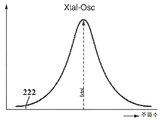
도 3은 크리스털의 개략적인 주파수-진폭 그래프를 도시한 도면이다.
도 4는 본 개시의 특정 예시의 실시예에 따른, 주기적인 킥스타터를 구비한 크리스털 발진기의 개략적인 회로 및 블록도이다.
도 5는 본 개시의 또 하나의 특정 예시의 실시예에 따른, 주기적인 킥스타터를 구비한 크리스털 발진기의 개략적인 회로 및 블록도이다.
도 6은 본 개시의 다른 또 하나의 특정 예시의 실시예에 따른, 주기적인 킥스타터를 구비한 크리스털 발진기의 개략적인 회로 및 블록도이다.
도 7은 본 개시의 교시에 따른, 크리스털의 주파수 대역폭 내의 킥-스타트 펄스들을 나타내는 크리스털의 개략적인 주파수-진폭 그래프를 도시한 도면이다.
도 8은 본 개시의 교시에 따른, 크리스털의 주파수 대역폭 내의 킥-스타트 펄스들을 이용하는 크리스털 발진기의 시동의 개략적인 주파수-진폭 그래프들을 도시한 도면이다.
도 9는 도 6에 도시된 특정 예시의 실시예에 따른, 킥-스타트 펄서(pulser)를 인에이블/디스에이블하기 위한 크리스털 발진기 출력 진폭 레벨 검출기의 개략도이다.
도 10은 본 개시의 특정 예시의 실시예들에 따른, 킥-스타트 펄서 회로의 개략도이다.
도 11은 본 개시의 교시에 따른, 도 4, 도 5 또는 도 6에 도시된 크리스털 발진기 회로를 포함하는 마이크로컨트롤러의 개략적인 블록도이다.
본 개시는 다양한 변형들 및 대안의 형태들이 쉽게 가능하지만, 그의 특정 예시의 실시예들이 도면들에 도시되었고 본 명세서에서 상세히 설명된다. 하지만, 여기서 그 특정 예시의 실시예들에 대한 설명은 본 개시를 여기에서 개시된 특정 형태들로 한정하고자 하는 것이 아님을 이해해야 할 것이다.The present disclosure may be more fully understood by reference to the following description taken in conjunction with the accompanying drawings.
Figure 1 is a schematic diagram of a crystal oscillator circuit.
Figure 2 is a schematic diagram of a crystal oscillator with a single pulse kick-start circuit.
3 shows a schematic frequency-amplitude graph of a crystal.
4 is a schematic circuit diagram and block diagram of a crystal oscillator with periodic kickstarter, in accordance with an embodiment of a specific example of the present disclosure.
5 is a schematic circuit diagram and block diagram of a crystal oscillator with a periodic kickstarter, in accordance with another specific example embodiment of the present disclosure;
6 is a schematic circuit and block diagram of a crystal oscillator with a periodic kickstarter, in accordance with another exemplary specific embodiment of the present disclosure;
7 is a diagram of a schematic frequency-amplitude plot of a crystal showing kick-start pulses in the frequency bandwidth of a crystal, in accordance with the teachings of the present disclosure;
8 is a diagram illustrating schematic frequency-amplitude plots of the start-up of a crystal oscillator using kick-start pulses in the frequency bandwidth of a crystal, in accordance with the teachings of the present disclosure;
9 is a schematic diagram of a crystal oscillator output amplitude level detector for enabling / disabling a kick-start pulser, according to an embodiment of the particular example shown in FIG. 6;
10 is a schematic diagram of a kick-start pulser circuit, in accordance with embodiments of certain illustrative aspects of the present disclosure.
FIG. 11 is a schematic block diagram of a microcontroller including the crystal oscillator circuit shown in FIG. 4, FIG. 5, or FIG. 6, in accordance with the teachings of the present disclosure.
While this disclosure is susceptible to various modifications and alternative forms, embodiments of specific examples thereof have been shown in the drawings and are herein described in detail. It should be understood, however, that the description of the embodiments of specific examples herein is not intended to limit the disclosure to the specific forms disclosed herein.
본 개시의 다양한 실시예들에 따르면, 크리스털 발진기 공진 주파수에 가까운 펄스 반복 속도를 갖는 펄싱 발진기는 크리스털 발진기 회로에 보다 유용한 시동 에너지를 제공하며, 따라서 훨씬 더 빠른 시동 시간을 제공한다. 시동 펄싱 발진기는 예를 들어 16 내지 64 펄스들(이것으로 한정되지 않음)을 실행하거나, 또는 크리스털 발진기 진폭이 소망 값으로 증가할 때까지 실행될 수 있다.According to various embodiments of the present disclosure, a pulsing oscillator having a pulse repetition rate close to the crystal oscillator resonant frequency provides more useful starting energy to the crystal oscillator circuit, thus providing much faster start-up time. The starter pulsing oscillator may be implemented, for example, without limitation, 16 to 64 pulses, or until the crystal oscillator amplitude increases to the desired value.
이제 도면들을 보면, 예시적인 실시예들의 세부 사항들이 개략적으로 도시되어 있다. 도면들에서 같은 요소들은 같은 번호들로 나타내어지며, 유사한 요소들은 같은 번호들에 다른 소문자 첨자를 붙여서 나타내어질 것이다.Turning now to the drawings, details of exemplary embodiments are schematically illustrated. In the drawings, like elements are denoted by like numerals, and like elements are denoted by the same numerals with different lower case subscripts.
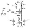
도 1을 보면, 크리스털 발진기 회로의 개략도가 도시되어 있다. 개괄적으로 번호 100으로 표시된 이 크리스털 발진기 회로는 전류원(102), 제 1 저항기(104), P-채널 금속 산화막 반도체(PMOS) 전계 효과 트랜지스터(FET)(106), 제 1 커패시터(108), 제 2 저항기(110), 크리스털 주파수 결정 요소(112), 제 2 커패시터(114), 제 3 커패시터(116), 및 PMOS FET(106)과 함께 토템 폴(totem pole) 회로 구성으로 구성된 NMOS FET(118)을 포함할 수 있다. 크리스털 발진기 회로(100)는 자신의 발진을 시동시키기 위해 회로 노이즈 에너지에 의존하고, 완전한 동작 발진 출력까지 도달하는데 가장 긴 시간을 필요로 한다. 32 KHz에서 발진하는 크리스털 발진기 회로(100)는 시동까지 최대 3 내지 4초가 걸릴 수 있고, 32 MHz 발진기는 시동을 위해 약 5 내지 20 밀리초가 걸릴 수 있다.Referring to Figure 1, a schematic diagram of a crystal oscillator circuit is shown. This crystal oscillator circuit, generally designated 100, includes a
이것은 표준 크리스털 발진기 회로 설계이며, 전자 회로 설계 분야에서 통상의 지식을 갖고 본 개시의 혜택을 갖는 자라면, 똑같이 잘 동작하는 다른 크리스털 발진기 회로 설계들을 쉽게 생각해 낼 수 있을 것이다. 이들 다른 크리스털 발진기 회로들 모두는 본 개시에 적용 가능하며 본 명세서에서 예상된다.This is a standard crystal oscillator circuit design, and those of ordinary skill in the electronics design arts and who have the benefit of this disclosure will readily be able to come up with other crystal oscillator circuit designs that work equally well. All of these other crystal oscillator circuits are applicable to this disclosure and are contemplated herein.
도 2를 보면, 단일 펄스 킥-스타트 회로를 구비한 크리스털 발진기의 개략도가 도시되어 있다. 이것은 도 1에 도시된 것과 동일한 크리스털 발진기 회로(100)이지만, 크리스털 발진기 회로(100)에 단일 펄스(222)로 에너지를 제공하는 킥-스타트 스위치(220)를 포함하는 킥-스타트 입력부를 갖는다. 이 단일 펄스(222)는 크리스털 발진기 회로(100)를 시동시키는데 유용한 매우 적은 에너지를 갖는데, 그 이유는 단일 펄스(222)가 크리스털 대역폭 내에서 매우 적은 에너지량으로 넓은 주파수 스펙트럼을 가지기 때문이다. 이 펄스의 에너지 중 작은 부분만이 도 3에 도시된 바와 같이 크리스털 대역폭 범위에 속할 것이다. 또한 단일 킥-스타트 펄스의 에너지는 주파수의 역함수이므로, 발진기의 주파수가 높을수록 단일 킥-스타터 회로의 효율성이 낮아질 것이다. 시뮬레이션 결과에 따르면, 도 2의 크리스털 발진기는 단일 펄스(222) 킥-스타트 이후에 약 2,000 내지 8,000 사이클을 필요로 할 수 있음이 나타났다. 기생 회로 커패시턴스들도 또한 단일 펄스로부터 에너지를 감쇠시킬 수 있으며, 때로는 크리스털 발진기가 전혀 시동되지 않을 수 있다.Turning now to Fig. 2, a schematic diagram of a crystal oscillator with a single pulse kick-start circuit is shown. This has a kick-start input that includes a kick-
도 4를 보면, 본 개시의 특정 예시의 실시예에 따른, 주기적인 킥스타터를 구비한 크리스털 발진기의 개략적인 회로 및 블록도가 도시되어 있다. 개괄적으로 번호 400으로 표시된, 주기적인 킥스타터를 구비한 이 크리스털 발진기는 크리스털 발진기 회로(100), 킥-스타트 펄서(434), 인버터들(438 및 440), 발진기 카운터(442) 및 AND 게이트(444)를 포함할 수 있다. 킥-스타트 펄서(434)는 크리스털(112)의 중심 주파수의 약 1/3 내지 약 1/2의 펄스 반복 속도(주파수)를 가질 수 있다. 이 반복 속도들은 크리스털 발진기 회로(100)에 실질적인 에너지를 제공할 수 있으며, 자신의 기본 주파수와 고조파 주파수를 갖는 이 주기 신호는 크리스털 발진기 회로(100)를 여기시킬 수 있다. 펄서 킥킹(kicking) 주파수는 크리스털의 중심 주파수의 10진(decade) 내에 있을 수 있고, 본 개시의 특정 예시적인 실시예들에 유효할 수 있음이 예상되고 본 개시의 범위 내에 있다.Turning now to Fig. 4, there is shown a schematic circuit and block diagram of a crystal oscillator with a periodic kickstarter, in accordance with an embodiment of a specific example of the present disclosure. This crystal oscillator with periodic kickstarter, generally designated at 400, includes a
크리스털 발진기 회로(100)는 킥-스타트 펄서(434)로 예를 들어 16-32회 펄싱될 수 있지만 이것으로 한정되지 않으며, 이로써 도 7에 도시된 바와 같이 크리스털(112)의 주파수 대역 통과 범위 내로 상당량의 에너지를 공급할 수 있다. 킥-스타트 펄서(434)는, 크리스털(112)의 L-C 탱크 회로를 자신의 기본 및 고조파 에너지를 사용하여 효과적으로 여기시키는 주기적 신호를 제공한다. 전형적으로, 주기적인 킥-스타트를 갖는 크리스털 발진기(400)는 임의의 펄스 여기 없이도 단지 크리스털 발진기 회로(100)보다 10배보다 더 빠르게 시작될 수 있다. 크리스털 발진기는 일단 크리스털 발진이 설정되면 발진을 유지하기 위해 더 작은 gm을 필요로 한다. 따라서, 더 높은 에너지 킥-스타터를 사용하면, 크리스털 발진기는 더 낮은 전력으로 구동될 수 있다.The
발진기 카운터(442)는 크리스털 발진기 회로(100)가 인버터(438)를 구동하기에 충분한 출력 전압 진폭을 갖는 시간으로부터 사이클들의 수를 모니터링한다. 충분한 수의 사이클들(예를 들어, 2048 또는 4096)이 발진기 카운터(442)에 의해 카운트될 때, 그것의 오버플로우 출력은 AND 게이트(444)의 출력부로부터 발진기 클록을 인에이블하고, 킥-스타트 펄서(434)를 디스에이블할 것이다. 카운터(442)의 리셋은 파워-온-리셋 또는 외부 리셋 명령(미도시됨)에 의해 수행될 수 있다.The
도 8은, 크리스털의 주파수 대역폭 내의 킥-스타트 펄스들을 이용하는 경우 및 킥-스타트 펄스들이 없는 경우(하부 그래프)를 대비하여(versus) 크리스털 발진기의 시동의 개략적인 주파수-진폭 그래프들을 도시한다. 킥 스타트 펄서(434)로부터의 주기적 펄스들을 가진 크리스털 발진기 출력 진폭(상부 그래프)에서 더 빠른 출력 진폭 증가가 도시되어 있다.Figure 8 shows schematic frequency-amplitude plots of the start-up of a crystal oscillator versus when using kick-start pulses in the frequency bandwidth of the crystal and in the absence of kick-start pulses (bottom graph). A faster output amplitude increase in the crystal oscillator output amplitude (top graph) with periodic pulses from the
도 5를 보면, 본 개시의 또 하나의 특정 예시의 실시예에 따른, 주기적인 킥스타터를 구비한 크리스털 발진기의 개략적인 회로 및 블록도가 도시되어 있다. 개괄적으로 번호 500으로 표시된, 주기적인 킥스타터를 구비한 이 크리스털 발진기는 크리스털 발진기 회로(100), 킥-스타트 펄서(434), 인버터들(438 및 440), 발진기 카운터(442), AND 게이트(444), 및 킥-스타트 펄서 카운터(536)를 포함할 수 있다. 크리스털 발진기(500)는 위에 설명된 크리스털 발진기(400)와 실질적으로 동일하게 동작한다. 그러나, 킥-스타트 펄서(434)로부터의 펄스들의 수, 예를 들어 64(이것으로 한정되지 않음)를 제한하기 위해 킥-스타트 펄서 카운터(536)가 추가되었다.Turning now to FIG. 5, there is shown a schematic circuit and block diagram of a crystal oscillator with a periodic kickstarter, in accordance with another specific example embodiment of the present disclosure. This crystal oscillator with periodic kickstarter, generally indicated at 500, includes a
도 6을 보면, 본 개시의 다른 또 하나의 특정 예시의 실시예에 따른, 주기적인 킥스타터를 구비한 크리스털 발진기의 개략적인 회로 및 블록도가 도시되어 있다. 개괄적으로 번호 600으로 표시된, 주기적인 킥스타터를 구비한 이 크리스털 발진기는 크리스털 발진기 회로(100), 킥-스타트 펄서(434), 인버터들(438, 440 및 656), AND 게이트(444), 발진기 출력 진폭 대 DC 레벨 컨버터(654), 전압 비교기(650) 및 전압 기준부(652)를 포함할 수 있다. 크리스털 발진기(600)는 보다 상세하게 전술한 바와 같이 킥-스타트 펄서(434)로부터의 여기와 관련하여 크리스털 발진기들(400 및 500)이 동작하는 것과 실질적으로 동일한 방식으로 동작한다. 그러나 킥-스타트 펄스들 및/또는 발진기 시동 사이클들의 수를 카운트하는 대신에, 간단한 피크 전압 검출기가 제공되어, 크리스털 발진기 회로(100)의 출력 진폭이 소망 진폭 값에 도달할 때 킥-스타트 펄서(434)는 디스에이블되고 AND 게이트(444)로부터의 발진기 클록 출력이 인에이블된다. 도 6의 이러한 피크 검출기 회로에 의해, 킥-스타트 펄서(434)는 크리스털 발진기 회로(100)로부터의 소망 출력 진폭이 달성되자마자 디스에이블될 것이고, AND 게이트(444)로부터의 발진기 클록 출력이 인에이블될 것이다. 또한, 크리스털 발진기 회로(100)의 출력 진폭이 소망 진폭 값보다 작아지면, 킥-스타트 펄서(434)는 다시 인에이블될 수 있고 그리고 AND 게이트(444)의 출력으로부터의 발진기 클록이 금지된다(디스에이블된다).Turning now to Fig. 6, there is shown a schematic circuit and block diagram of a crystal oscillator with a periodic kickstarter, in accordance with another exemplary specific embodiment of the present disclosure. This crystal oscillator with periodic kickstarter, generally designated as
도 9를 보면, 도 6에 도시된 특정 예시의 실시예에 따른, 킥-스타트 펄서를 위한 크리스털 발진기 출력 진폭 레벨 검출기 및 인에이블/디스에이블 회로의 개략도가 도시되어 있다. 간단한 다이오드 정류기(654) 또는 포락선 검출기 회로는 고주파수 발진기 파형을 정류하고 발진기 출력 파형의 진폭을 나타내는 DC 전압 레벨을 제공하는데 사용될 수 있다. RC 저역 통과 필터는 다이오드 정류기(654)의 출력부와 전압 비교기(650)의 제 1 입력부 사이에 결합될 수 있다. 전압 비교기(650)의 제 2 입력부는 전압 기준부(652)에 결합된다. 도 9에 도시된 회로 구성에서, 제 1 입력부(+)의 전압이 전압 기준부(652)의 기준 전압보다 클 때마다, 그것의 출력은 로직 하이가 되고, AND 게이트(444)로부터의 클록 발진기 출력을 인에이블하고 킥-스타트 펄서(434)를 디스에이블하는데 사용될 수 있다.Turning to Fig. 9, there is shown a schematic diagram of a crystal oscillator output amplitude level detector and enable / disable circuit for a kick-start pulser, according to an embodiment of the specific example shown in Fig. A
도 10을 보면, 본 개시의 특정 예시의 실시예들에 따른, 킥-스타트 펄서 회로의 개략도가 도시되어 있다. 킥-스타트 펄서(434)는 전류원(1060), 타이밍 커패시터(1062), 스위치들(1064 및 1068), 및 히스테리시스를 갖는 비교기(1066)를 포함할 수 있다. 전류원(1060)이 커패시터(1062)를 충전함에 따라, 커패시터의 플레이트들 양단 전압은 상승한다. 커패시터(1062)의 양단 전압은 비교기(1066)에 의해 감지된다. 전압이 비교기(1066)의 임계 전압과 교차할 때, 그것의 출력은 로직 레벨들을 변화시키고, 이 로직 레벨들은 커패시터(1062)의 두 개의 플레이트들을 가로질러 연결된 스위치(1064)를 교대로 제어한다. 비교기(1066)의 출력이 로직 로우가 될 때, 그것은 커패시터(1062) 양단에 걸쳐 있는 스위치(1064)를 인에이블(폐쇄)하고 커패시터(1062)의 두 플레이트들을 함께 단락시킴으로써, 이들 사이의 임의의 전압 차를 제거한다. 커패시터(1062)의 플레이트들 양단 전압이 실질적으로 0V로 떨어지면, 비교기(1066) 출력은 로직 하이로 복귀하고 커패시터(1062) 양단에 걸쳐 있는 스위치(1064)를 디스에이블(개방)시킴으로써, 전류원(1060)이 커패시터(1062) 상의 전압을 다시 충전하기 시작할 수 있게 한다. 이러한 커패시터(1062)의 충전 및 방전은 크리스털 발진기 회로(434)를 펄싱하는데 사용되는 주기적 파형을 생성한다. 도 10에 도시된 킥-스타트 펄서(434) 회로는 클록 생성기 회로를 나타낸다. 전자 회로 설계 분야의 당업자이고 본 개시의 혜택을 갖는 자라면, 본 명세서에 설명된 킥-스타트 회로들과 함께 사용될 수 있는 주기적인 파형들을 생성하는 여러 상이한 회로 설계들을 용이하게 생각해 낼 수 있다.Turning now to Fig. 10, a schematic diagram of a kick-start pulser circuit is shown, in accordance with certain exemplary embodiments of the present disclosure. The kick-
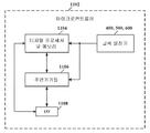
도 11을 보면, 본 개시의 교시에 따른, 도 4, 도 5 또는 도 6에 도시된 크리스털 발진기 회로를 포함하는 마이크로컨트롤러의 개략적인 블록도가 도시되어 있다. 마이크로컨트롤러(1102)는 디지털 프로세서 및 메모리(1104), 주변기기 모듈들(1106), 입/출력부(1108) 및 클록 발진기(400, 500 또는 600)를 포함할 수 있다. 여기에 개시된 크리스털 발진기 실시예들은 마이크로컨트롤러(1102)가 더 일찍 동작을 시작할 수 있게 하는데, 그 이유는 킥-스타트 펄서(434)가 크리스털 발진기 회로를 구비하지 않는 경우보다 짧은 시간에 클록 발진기 출력이 이용 가능하고 안정적이기 때문이다.Turning now to Fig. 11, there is shown a schematic block diagram of a microcontroller including the crystal oscillator circuit shown in Figs. 4, 5, or 6, in accordance with the teachings of the present disclosure. The
Claims (22)
상기 외부 크리스털과 결합된 발진기 회로; 및
상기 발진기 회로에 결합되어 상기 발진기 회로에 시동 에너지를 펄싱하는 킥-스타트 펄서를 포함하는 시동 회로를 포함하는, 집적 발진기.An integrated oscillator configured to couple with an external crystal,
An oscillator circuit coupled with the outer crystal; And
And a kick-start pulser coupled to the oscillator circuit for pulsing startup energy to the oscillator circuit.
상기 킥-스타트 펄서는 커패시터를 충전하는 전류원, 상기 커패시터와 병렬로 결합된 방전 스위치 - 상기 전류원과 상기 커패시터 사이의 노드는 비교기의 입력부에 결합되고 상기 비교기의 출력부는 상기 방전 스위치를 제어함 -, 및 상기 비교기에 의해 제어되고 상기 발진기 회로에 결합된 펄싱 스위치를 포함하는, 집적 발진기.The method according to claim 1,
The kick-start pulser having a current source for charging a capacitor, a discharge switch coupled in parallel with the capacitor, a node between the current source and the capacitor being coupled to an input of the comparator, and an output of the comparator controlling the discharge switch, And a pulsing switch controlled by the comparator and coupled to the oscillator circuit.
상기 비교기는 히스테리시스를 갖는, 집적 발진기.3. The method according to claim 1 or 2,
Wherein the comparator has a hysteresis.
소정 개수의 펄스들이 상기 시동 회로에 의해 생성된 후에 상기 시동 회로를 디스에이블하는 디지털 카운터를 더 포함하는 집적 발진기.4. The method according to any one of claims 1 to 3,
And a digital counter that disables the starter circuit after a predetermined number of pulses have been generated by the starter circuit.
상기 소정 개수의 펄스들은 약 16 내지 약 32 펄스들인, 집적 발진기.5. The method according to any one of claims 1 to 4,
The predetermined number of pulses being from about 16 to about 32 pulses.
상기 소정 개수의 펄스들은 약 32 내지 약 64 펄스들인, 집적 발진기.6. The method according to any one of claims 1 to 5,
The predetermined number of pulses being from about 32 pulses to about 64 pulses.
상기 킥-스타트 펄서의 주파수는 상기 외부 크리스털의 중심 주파수의 약 1/3 내지 약 1/2인, 집적 발진기.7. The method according to any one of claims 1 to 6,
Wherein the frequency of the kick-start pulser is about 1/3 to about 1/2 the center frequency of the outer crystal.
상기 킥-스타트 펄서의 주파수는 상기 외부 크리스털의 중심 주파수의 10진(decade) 이내인, 집적 발진기.8. The method according to any one of claims 1 to 7,
Wherein the frequency of the kick-start pulser is within a decade of the center frequency of the outer crystal.
상기 킥-스타트 펄서의 주파수는 상기 외부 크리스털의 대역 통과 주파수 이내인, 집적 발진기.9. The method according to any one of claims 1 to 8,
Wherein the frequency of the kick-start pulser is within a band-pass frequency of the outer crystal.
상기 마이크로컨트롤러는 상기 발진기 회로가 안정된 발진 진폭을 가진 이후에 상기 시동 회로를 턴 오프하도록 구성되는, 마이크로컨트롤러.11. The method of claim 10,
Wherein the microcontroller is configured to turn off the starter circuit after the oscillator circuit has a stable oscillation amplitude.
상기 마이크로컨트롤러는 상기 마이크로컨트롤러가 동작하기 시작한 후 소정의 시간 주기 이후에 상기 시동 회로를 턴 오프하도록 구성되는, 마이크로컨트롤러.11. The method of claim 10,
Wherein the microcontroller is configured to turn off the starter circuit after a predetermined period of time after the microcontroller starts operating.
상기 발진기 회로는,
공급 전압부에 결합된 전류원;
바이어스 전압에 결합된 제 1 저항기;
상기 제 1 저항기에 결합된 제 1 커패시터;
상기 제 1 커패시터에 결합된 제 2 저항기;
상기 전류원, 제 1 커패시터, 및 제 1 및 제 2 저항기들에 결합된 제 1 트랜지스터;
상기 제 1 커패시터와 제 2 저항기에 결합된 제 2 커패시터;
상기 제 2 저항기와 제 1 트랜지스터에 결합된 제 3 커패시터;
상기 제 1, 제 2 및 제 3 커패시터들, 상기 제 2 저항기 및 상기 제 1 트랜지스터에 결합된 제 2 트랜지스터; 및
상기 제 1 및 제 2 트랜지스터들, 상기 제 1, 제 2 및 제 3 커패시터들, 및 상기 제 2 저항기에 결합된 상기 외부 크리스털을 포함하는, 집적 발진기.13. The method according to any one of claims 1 to 12,
Wherein the oscillator circuit comprises:
A current source coupled to the supply voltage portion;
A first resistor coupled to the bias voltage;
A first capacitor coupled to the first resistor;
A second resistor coupled to the first capacitor;
A first transistor coupled to the current source, the first capacitor, and the first and second resistors;
A second capacitor coupled to the first capacitor and the second resistor;
A third capacitor coupled to the second resistor and the first transistor;
A second transistor coupled to the first, second and third capacitors, the second resistor and the first transistor; And
The first and second transistors, the first, second and third capacitors, and the external crystal coupled to the second resistor.
크리스털 발진기;
상기 크리스털 발진기에 결합된 킥-스타트 펄서;
상기 크리스털 발진기에 결합된 발진기 사이클 카운터; 및
발진기 클록 출력을 인에이블 및 디스에이블하기 위한 로직 게이트를 포함하고,
상기 발진기 사이클 카운터는 상기 킥-스타트 펄서를 디스에이블하고, 상기 발진기로부터의 소정 개수의 사이클들이 카운트된 이후에 상기 로직 게이트로부터 상기 발진기 클록 출력을 인에이블하는, 집적 발진기.An integrated oscillator configured to couple with an external crystal,
Crystal oscillator;
A kick-start pulser coupled to the crystal oscillator;
An oscillator cycle counter coupled to the crystal oscillator; And
And a logic gate for enabling and disabling the oscillator clock output,
Wherein the oscillator cycle counter disables the kick-start pulser and enables the oscillator clock output from the logic gate after a predetermined number of cycles from the oscillator have been counted.
상기 킥-스타트 펄서는 커패시터를 충전하는 전류원, 상기 커패시터와 병렬로 결합된 방전 스위치 - 상기 전류원과 상기 커패시터 사이의 노드는 비교기의 입력부에 결합되고 상기 비교기의 출력부는 상기 방전 스위치를 제어함 -, 및 상기 비교기에 의해 제어되고 상기 발진기 회로에 결합된 펄싱 스위치를 포함하는, 집적 발진기.15. The method of claim 14,
The kick-start pulser having a current source for charging a capacitor, a discharge switch coupled in parallel with the capacitor, a node between the current source and the capacitor being coupled to an input of the comparator, and an output of the comparator controlling the discharge switch, And a pulsing switch controlled by the comparator and coupled to the oscillator circuit.
상기 킥-스타트 펄서에 결합된 킥-스타트 펄서 카운터를 더 포함하고,
상기 킥-스타트 펄서는 소정 개수의 펄스들이 상기 킥-스타트 펄서 카운터에 의해 카운트된 이후에 디스에이블되는, 집적 발진기.16. The method according to claim 14 or 15,
Further comprising a kick-start pulsar counter coupled to the kick-start pulser,
Wherein the kick-start pulsar is disabled after a predetermined number of pulses have been counted by the kick-start pulsar counter.
크리스털 발진기;
상기 크리스털 발진기에 결합된 킥-스타트 펄서;
발진기 클록 출력을 인에이블 및 디스에이블하기 위한 로직 게이트;
상기 크리스털 발진기에 결합된 발진기 출력 진폭 검출기;
기준 전압을 제공하는 전압 기준부; 및
상기 발진기 출력 진폭 검출기에 결합된 제 1 입력부, 및 상기 전압 기준부에 결합된 제 2 입력부를 구비한 전압 비교기를 포함하고,
상기 검출된 발진기 출력 진폭이 상기 기준 전압보다 클 때, 상기 킥-스타트 펄서는 디스에이블되고 상기 로직 게이트는 인에이블되어 상기 발진기 클록 출력을 제공하는, 집적 발진기.An integrated oscillator configured to couple with an external crystal,
Crystal oscillator;
A kick-start pulser coupled to the crystal oscillator;
A logic gate for enabling and disabling the oscillator clock output;
An oscillator output amplitude detector coupled to the crystal oscillator;
A voltage reference unit for providing a reference voltage; And
A voltage comparator having a first input coupled to the oscillator output amplitude detector and a second input coupled to the voltage reference,
Wherein when the detected oscillator output amplitude is greater than the reference voltage, the kick-start pulser is disabled and the logic gate is enabled to provide the oscillator clock output.
상기 킥-스타트 펄서는 커패시터를 충전하는 전류원, 상기 커패시터와 병렬로 결합된 방전 스위치 - 상기 전류원과 상기 커패시터 사이의 노드는 비교기의 입력부에 결합되고 상기 비교기의 출력부는 상기 방전 스위치를 제어함 -, 및 상기 비교기에 의해 제어되고 상기 발진기 회로에 결합된 펄싱 스위치를 포함하는, 집적 발진기.19. The method of claim 18,
The kick-start pulser having a current source for charging a capacitor, a discharge switch coupled in parallel with the capacitor, a node between the current source and the capacitor being coupled to an input of the comparator, and an output of the comparator controlling the discharge switch, And a pulsing switch controlled by the comparator and coupled to the oscillator circuit.
발진기 회로를 상기 외부 크리스털에 결합시키는 단계; 및
상기 발진기 회로에 결합된 킥-스타트 펄서를 사용하여 상기 발진기 회로 내에 에너지를 펄싱하는 단계를 포함하는, 방법.CLAIMS What is claimed is: 1. A method for starting an integrated oscillator configured to be coupled to an external crystal,
Coupling an oscillator circuit to the outer crystal; And
And pulsing energy into the oscillator circuit using a kick-start pulser coupled to the oscillator circuit.
상기 킥-스타트 펄서 내에 에너지를 펄싱하는 단계는,
전류원을 사용하여 커패시터를 충전하는 단계;
상기 커패시터의 전압에 도달할 때 히스테리시스를 갖는 비교기에 의해 제어되는 스위치를 사용하여 상기 커패시터를 방전하는 단계; 및
상기 비교기를 사용하여 펄싱 스위치를 스위칭 온 및 오프하는 단계를 포함하고,
상기 펄싱 스위치는 상기 펄싱 에너지를 상기 발진기 회로에 제공하는, 방법.22. The method of claim 21,
Pulsing energy in the kick-start pulser,
Charging the capacitor using a current source;
Discharging the capacitor using a switch controlled by a comparator having a hysteresis when the voltage of the capacitor is reached; And
Switching the pulsing switch on and off using the comparator,
Wherein the pulsing switch provides the pulsing energy to the oscillator circuit.
Applications Claiming Priority (5)
| Application Number | Priority Date | Filing Date | Title |
|---|---|---|---|
| US201562183027P | 2015-06-22 | 2015-06-22 | |
| US62/183,027 | 2015-06-22 | ||
| US15/186,034 | 2016-06-17 | ||
| US15/186,034 US10135390B2 (en) | 2015-06-22 | 2016-06-17 | Periodic kick-starter for a crystal oscillator |
| PCT/US2016/038465 WO2016209791A1 (en) | 2015-06-22 | 2016-06-21 | Periodic kickstarter for a crystal oscillator |
Publications (1)
| Publication Number | Publication Date |
|---|---|
| KR20180020211A true KR20180020211A (en) | 2018-02-27 |
Family
ID=56418591
Family Applications (1)
| Application Number | Title | Priority Date | Filing Date |
|---|---|---|---|
| KR1020187000746A KR20180020211A (en) | 2015-06-22 | 2016-06-21 | Periodic kickstarter for crystal oscillators |
Country Status (7)
| Country | Link |
|---|---|
| US (1) | US10135390B2 (en) |
| EP (1) | EP3311491A1 (en) |
| JP (1) | JP2018518901A (en) |
| KR (1) | KR20180020211A (en) |
| CN (1) | CN107787552B (en) |
| TW (1) | TW201711373A (en) |
| WO (1) | WO2016209791A1 (en) |
Families Citing this family (12)
| Publication number | Priority date | Publication date | Assignee | Title |
|---|---|---|---|---|
| WO2017068690A1 (en) * | 2015-10-22 | 2017-04-27 | オリンパス株式会社 | Optical scanning device and method for controlling optical scanning device |
| US10367450B2 (en) * | 2015-12-15 | 2019-07-30 | Mediatek Inc. | Oscillator scheme capable of reducing far-out phase noise and closed-in phase noise |
| JP6809115B2 (en) * | 2016-10-13 | 2021-01-06 | セイコーエプソン株式会社 | Circuits, oscillators, electronics and mobiles |
| US10411649B2 (en) | 2017-03-02 | 2019-09-10 | Spreadtrum Communications Usa Inc. | Low-power crystal oscillator operating in class B with positive feedback and a step-down voltage regulator |
| US10432143B2 (en) * | 2017-12-25 | 2019-10-01 | Shenzhen GOODIX Technology Co., Ltd. | Circuit and method for facilitating startup time of crystal oscillator |
| CN109314519B (en) * | 2018-09-14 | 2023-01-24 | 深圳市汇顶科技股份有限公司 | Computer readable storage medium, fast start clock system and control method thereof |
| US10673383B2 (en) | 2018-09-20 | 2020-06-02 | Silicon Laboratories Inc. | Clock circuit and method for recalibrating an injection oscillator coupled to kick-start a crystal oscillator |
| US10965382B1 (en) * | 2020-01-09 | 2021-03-30 | Texas Instruments Incorporated | Oscillator for pulse communication with reduced startup latency |
| CN111404488B (en) * | 2020-03-27 | 2023-11-03 | 维沃移动通信有限公司 | Electronic equipment |
| EP4087123A1 (en) * | 2021-05-06 | 2022-11-09 | Nordic Semiconductor ASA | Oscillator circuits |
| CN115580292A (en) | 2021-06-21 | 2023-01-06 | 联发科技股份有限公司 | Crystal Oscillator and Its Starting Method |
| US12166853B2 (en) | 2022-10-24 | 2024-12-10 | Mediatek Singapore Pte. Ltd. | Push-start crystal oscillator, associated electronic device and push-start method for performing start-up procedure of crystal oscillator |
Family Cites Families (17)
| Publication number | Priority date | Publication date | Assignee | Title |
|---|---|---|---|---|
| JPS63113309U (en) * | 1987-01-16 | 1988-07-21 | ||
| JPS63204906A (en) * | 1987-02-20 | 1988-08-24 | Sanyo Electric Co Ltd | Abnormal lock detection circuit |
| JPS63187412U (en) * | 1987-05-22 | 1988-11-30 | ||
| US5594388A (en) * | 1995-06-07 | 1997-01-14 | American Microsystems, Inc. | Self-calibrating RC oscillator |
| JPH11186848A (en) * | 1997-12-18 | 1999-07-09 | Oki Electric Ind Co Ltd | Oscillation circuit |
| JPH11284438A (en) * | 1998-03-27 | 1999-10-15 | Kinseki Ltd | Piezoelectric oscillator |
| JP2003032039A (en) * | 2001-07-16 | 2003-01-31 | Toyo Commun Equip Co Ltd | Piezoelectric oscillation circuit |
| AU2003274640A1 (en) | 2002-10-16 | 2004-05-04 | Rfwaves Ltd. | Method and system for fast wake-up of oscillators |
| TWI300650B (en) * | 2003-04-24 | 2008-09-01 | Int Rectifier Corp | Fault protected self-oscillating driver |
| DE102006009644A1 (en) | 2006-01-04 | 2007-07-05 | Biotronik Crm Patent Ag | Phase-locked loop for frequency synthesis, has phase detector or phase frequency detector and adjustable oscillator whereby frequency divider is connected with reference oscillator at end side over second switch |
| US7808327B2 (en) | 2006-08-07 | 2010-10-05 | Texas Instruments Incorporated | Method and apparatus to provide digitally controlled crystal oscillators |
| JP5200491B2 (en) * | 2006-11-06 | 2013-06-05 | セイコーエプソン株式会社 | Drive device, physical quantity measuring device and electronic device |
| CN101399504B (en) * | 2007-09-27 | 2011-05-11 | 智原科技股份有限公司 | All-digital soft-start circuit and power supply system using this circuit |
| JP2010147758A (en) * | 2008-12-18 | 2010-07-01 | Panasonic Corp | Oscillation circuit |
| JP5847505B2 (en) * | 2011-09-09 | 2016-01-20 | シチズンホールディングス株式会社 | Vibrator unit, oscillation circuit, and reception circuit |
| US8643445B1 (en) | 2012-08-08 | 2014-02-04 | Texas Instruments Incorporated | Crystal oscillator circuit |
| EP2884658A1 (en) * | 2013-12-16 | 2015-06-17 | Telefonaktiebolaget L M Ericsson (publ) | Oscillator circuit |
-
2016
- 2016-06-17 US US15/186,034 patent/US10135390B2/en active Active
- 2016-06-21 CN CN201680036534.7A patent/CN107787552B/en active Active
- 2016-06-21 WO PCT/US2016/038465 patent/WO2016209791A1/en unknown
- 2016-06-21 KR KR1020187000746A patent/KR20180020211A/en unknown
- 2016-06-21 EP EP16739607.6A patent/EP3311491A1/en not_active Ceased
- 2016-06-21 JP JP2017563205A patent/JP2018518901A/en active Pending
- 2016-06-22 TW TW105119619A patent/TW201711373A/en unknown
Also Published As
| Publication number | Publication date |
|---|---|
| CN107787552B (en) | 2021-09-03 |
| US20160373056A1 (en) | 2016-12-22 |
| JP2018518901A (en) | 2018-07-12 |
| US10135390B2 (en) | 2018-11-20 |
| WO2016209791A1 (en) | 2016-12-29 |
| EP3311491A1 (en) | 2018-04-25 |
| TW201711373A (en) | 2017-03-16 |
| CN107787552A (en) | 2018-03-09 |
Similar Documents
| Publication | Publication Date | Title |
|---|---|---|
| US10135390B2 (en) | Periodic kick-starter for a crystal oscillator | |
| KR102226978B1 (en) | Resonant capacitor stabilizer in resonant converters | |
| TWI493864B (en) | Osicillatting signal generatting device and related method | |
| KR20130020652A (en) | Failsafe oscillator monitor and alarm | |
| JP2018518901A5 (en) | ||
| CN101179266A (en) | Stable oscillator free from temperature change and supply voltage change | |
| US10050585B2 (en) | Ultra-low power crystal oscillator with adaptive self-start | |
| JP2003167642A (en) | Clock generation circuit and method | |
| US5341113A (en) | Voltage controlled oscillator having a 50% duty cycle | |
| TW200830718A (en) | Low-power oscillator | |
| Forrester et al. | Resonant current estimation and phase-locked loop control system for inductorless step-up single piezo element-based (SUPRC) DC-DC converter | |
| JP2024004518A (en) | semiconductor equipment | |
| JPH11186885A (en) | Clock signal control circuit | |
| TW201806302A (en) | Switching regulator | |
| US6771138B1 (en) | Method of forming a bi-directional synchronization controller | |
| TW201722046A (en) | Driving circuit for power switch | |
| JP5799825B2 (en) | DC-DC converter, semiconductor integrated circuit, and DC-DC conversion method | |
| EP4432558A2 (en) | Oscillator circuit | |
| EP2388915B1 (en) | Sawtooth oscillator | |
| Yu et al. | Half-bridge driver with charge pump based high-side voltage regulator | |
| TWI251398B (en) | Resistor-capacitor type oscillator circuit | |
| Schormans et al. | Intermittent Excitation of High-Q Resonators for Low-Power High-Speed Clock Generation | |
| JP2004242241A (en) | Crystal oscillation circuit | |
| JP6650722B2 (en) | Multi-frequency transceiver circuit | |
| US6486805B1 (en) | Frequency to digital converter |
Legal Events
| Date | Code | Title | Description |
|---|---|---|---|
| PA0105 | International application |
Patent event date: 20180109 Patent event code: PA01051R01D Comment text: International Patent Application |
|
| PG1501 | Laying open of application | ||
| PC1203 | Withdrawal of no request for examination |