KR20170041145A - Exposure apparatus, exposure method, and method of manufacturing devices - Google Patents
Exposure apparatus, exposure method, and method of manufacturing devices Download PDFInfo
- Publication number
- KR20170041145A KR20170041145A KR1020160128189A KR20160128189A KR20170041145A KR 20170041145 A KR20170041145 A KR 20170041145A KR 1020160128189 A KR1020160128189 A KR 1020160128189A KR 20160128189 A KR20160128189 A KR 20160128189A KR 20170041145 A KR20170041145 A KR 20170041145A
- Authority
- KR
- South Korea
- Prior art keywords
- mark
- light
- exposure
- substrate
- mask
- Prior art date
Links
Images


Classifications
-
- G—PHYSICS
- G03—PHOTOGRAPHY; CINEMATOGRAPHY; ANALOGOUS TECHNIQUES USING WAVES OTHER THAN OPTICAL WAVES; ELECTROGRAPHY; HOLOGRAPHY
- G03F—PHOTOMECHANICAL PRODUCTION OF TEXTURED OR PATTERNED SURFACES, e.g. FOR PRINTING, FOR PROCESSING OF SEMICONDUCTOR DEVICES; MATERIALS THEREFOR; ORIGINALS THEREFOR; APPARATUS SPECIALLY ADAPTED THEREFOR
- G03F7/00—Photomechanical, e.g. photolithographic, production of textured or patterned surfaces, e.g. printing surfaces; Materials therefor, e.g. comprising photoresists; Apparatus specially adapted therefor
- G03F7/70—Microphotolithographic exposure; Apparatus therefor
- G03F7/70216—Mask projection systems
- G03F7/70258—Projection system adjustments, e.g. adjustments during exposure or alignment during assembly of projection system
-
- G—PHYSICS
- G03—PHOTOGRAPHY; CINEMATOGRAPHY; ANALOGOUS TECHNIQUES USING WAVES OTHER THAN OPTICAL WAVES; ELECTROGRAPHY; HOLOGRAPHY
- G03F—PHOTOMECHANICAL PRODUCTION OF TEXTURED OR PATTERNED SURFACES, e.g. FOR PRINTING, FOR PROCESSING OF SEMICONDUCTOR DEVICES; MATERIALS THEREFOR; ORIGINALS THEREFOR; APPARATUS SPECIALLY ADAPTED THEREFOR
- G03F7/00—Photomechanical, e.g. photolithographic, production of textured or patterned surfaces, e.g. printing surfaces; Materials therefor, e.g. comprising photoresists; Apparatus specially adapted therefor
- G03F7/20—Exposure; Apparatus therefor
-
- G—PHYSICS
- G03—PHOTOGRAPHY; CINEMATOGRAPHY; ANALOGOUS TECHNIQUES USING WAVES OTHER THAN OPTICAL WAVES; ELECTROGRAPHY; HOLOGRAPHY
- G03F—PHOTOMECHANICAL PRODUCTION OF TEXTURED OR PATTERNED SURFACES, e.g. FOR PRINTING, FOR PROCESSING OF SEMICONDUCTOR DEVICES; MATERIALS THEREFOR; ORIGINALS THEREFOR; APPARATUS SPECIALLY ADAPTED THEREFOR
- G03F7/00—Photomechanical, e.g. photolithographic, production of textured or patterned surfaces, e.g. printing surfaces; Materials therefor, e.g. comprising photoresists; Apparatus specially adapted therefor
- G03F7/70—Microphotolithographic exposure; Apparatus therefor
- G03F7/70008—Production of exposure light, i.e. light sources
-
- G—PHYSICS
- G03—PHOTOGRAPHY; CINEMATOGRAPHY; ANALOGOUS TECHNIQUES USING WAVES OTHER THAN OPTICAL WAVES; ELECTROGRAPHY; HOLOGRAPHY
- G03F—PHOTOMECHANICAL PRODUCTION OF TEXTURED OR PATTERNED SURFACES, e.g. FOR PRINTING, FOR PROCESSING OF SEMICONDUCTOR DEVICES; MATERIALS THEREFOR; ORIGINALS THEREFOR; APPARATUS SPECIALLY ADAPTED THEREFOR
- G03F7/00—Photomechanical, e.g. photolithographic, production of textured or patterned surfaces, e.g. printing surfaces; Materials therefor, e.g. comprising photoresists; Apparatus specially adapted therefor
- G03F7/70—Microphotolithographic exposure; Apparatus therefor
- G03F7/70058—Mask illumination systems
- G03F7/70141—Illumination system adjustment, e.g. adjustments during exposure or alignment during assembly of illumination system
-
- G—PHYSICS
- G03—PHOTOGRAPHY; CINEMATOGRAPHY; ANALOGOUS TECHNIQUES USING WAVES OTHER THAN OPTICAL WAVES; ELECTROGRAPHY; HOLOGRAPHY
- G03F—PHOTOMECHANICAL PRODUCTION OF TEXTURED OR PATTERNED SURFACES, e.g. FOR PRINTING, FOR PROCESSING OF SEMICONDUCTOR DEVICES; MATERIALS THEREFOR; ORIGINALS THEREFOR; APPARATUS SPECIALLY ADAPTED THEREFOR
- G03F7/00—Photomechanical, e.g. photolithographic, production of textured or patterned surfaces, e.g. printing surfaces; Materials therefor, e.g. comprising photoresists; Apparatus specially adapted therefor
- G03F7/70—Microphotolithographic exposure; Apparatus therefor
- G03F7/70216—Mask projection systems
- G03F7/70258—Projection system adjustments, e.g. adjustments during exposure or alignment during assembly of projection system
- G03F7/70266—Adaptive optics, e.g. deformable optical elements for wavefront control, e.g. for aberration adjustment or correction
-
- G—PHYSICS
- G03—PHOTOGRAPHY; CINEMATOGRAPHY; ANALOGOUS TECHNIQUES USING WAVES OTHER THAN OPTICAL WAVES; ELECTROGRAPHY; HOLOGRAPHY
- G03F—PHOTOMECHANICAL PRODUCTION OF TEXTURED OR PATTERNED SURFACES, e.g. FOR PRINTING, FOR PROCESSING OF SEMICONDUCTOR DEVICES; MATERIALS THEREFOR; ORIGINALS THEREFOR; APPARATUS SPECIALLY ADAPTED THEREFOR
- G03F7/00—Photomechanical, e.g. photolithographic, production of textured or patterned surfaces, e.g. printing surfaces; Materials therefor, e.g. comprising photoresists; Apparatus specially adapted therefor
- G03F7/70—Microphotolithographic exposure; Apparatus therefor
- G03F7/70216—Mask projection systems
- G03F7/70275—Multiple projection paths, e.g. array of projection systems, microlens projection systems or tandem projection systems
-
- G—PHYSICS
- G03—PHOTOGRAPHY; CINEMATOGRAPHY; ANALOGOUS TECHNIQUES USING WAVES OTHER THAN OPTICAL WAVES; ELECTROGRAPHY; HOLOGRAPHY
- G03F—PHOTOMECHANICAL PRODUCTION OF TEXTURED OR PATTERNED SURFACES, e.g. FOR PRINTING, FOR PROCESSING OF SEMICONDUCTOR DEVICES; MATERIALS THEREFOR; ORIGINALS THEREFOR; APPARATUS SPECIALLY ADAPTED THEREFOR
- G03F7/00—Photomechanical, e.g. photolithographic, production of textured or patterned surfaces, e.g. printing surfaces; Materials therefor, e.g. comprising photoresists; Apparatus specially adapted therefor
- G03F7/70—Microphotolithographic exposure; Apparatus therefor
- G03F7/70691—Handling of masks or workpieces
- G03F7/70775—Position control, e.g. interferometers or encoders for determining the stage position
Abstract
Description
본 발명은 노광 장치, 노광 방법, 및 디바이스 제조 방법에 관한 것이다.The present invention relates to an exposure apparatus, an exposure method, and a device manufacturing method.
반도체 디바이스 등의 제조를 위한 리소그래피 공정에 있어서, 투영 광학계를 개재하여 기판의 노광 영역에 원판의 패턴을 전사하는 노광 장치가 사용된다. 디바이스 등이 소형화됨에 따라 노광 장치에 의해 전사되는 패턴의 선폭 균일성의 향상이 요구되고 있다. 선폭 균일성은 투영 광학계의 결상 성능의 변화에 의해 저하될 수 있다. 투영 광학계의 결상 성능의 변화는 투영 광학계에 포함되는 광학 요소의 진동으로 인해 발생할 수 있다. 일본 특허 공개 제2010-283089호는, 투영 광학계를 포함하는 각 부분의 진동을 센서에 의해 검지하고 검지된 진동에 기초하여 투영 광학계에 포함되는 광학 요소를 진동시킴으로써 선폭의 변화량을 저감하는 노광 장치를 개시한다. 일본 특허 공개 제2001-185478호는 투영 광학계에 포함되는 광학 요소의 자세 변동을 계측하고 계측 결과에 기초하여 원판이나 기판을 이동시킴으로써 자세 변동에 의해 발생되는 전사 위치의 편차를 보정하는 노광 장치를 개시한다.In a lithography process for manufacturing a semiconductor device or the like, an exposure apparatus for transferring a pattern of an original plate onto an exposure area of a substrate via a projection optical system is used. As a device or the like is miniaturized, it is required to improve the uniformity of the line width of the pattern transferred by the exposure apparatus. The line width uniformity can be lowered by a change in the imaging performance of the projection optical system. The change in the imaging performance of the projection optical system may occur due to the vibration of the optical element included in the projection optical system. Japanese Patent Application Laid-Open No. 2010-283089 discloses an exposure apparatus that detects a vibration of each part including a projection optical system by a sensor and vibrates the optical element included in the projection optical system based on the detected vibration to reduce the variation amount of the line width . Japanese Patent Application Laid-Open No. 2001-185478 discloses an exposure apparatus which corrects the deviation of the transfer position caused by the attitude change by measuring the attitude change of the optical element included in the projection optical system and moving the original plate or substrate based on the measurement result do.
상기 특허 문헌의 노광 장치에 의해 선폭 균일성을 향상시키기 위해, 장치에 포함하는 광학 요소에 부착되는 센서의 수 및 종류가 증가되어야 하지만, 이는 비용의 문제점 등의 관점에서 현실적이지 않다. 또한, 어느 노광 장치도 노광 영역에 전사된 패턴의 선폭의 변화량을 직접적으로 획득하지는 않지만, 검지된 진동량 등에 기초한 계산에 의해 간접적으로 획득하기 때문에, 계산 과정에 있어서 오차가 발생할 수 있다.In order to improve the uniformity of the line width by the exposure apparatus of the patent document, the number and types of sensors attached to the optical elements included in the apparatus should be increased, but this is not realistic from the viewpoint of cost and the like. Further, although any of the exposure apparatuses does not directly acquire the amount of change of the line width of the pattern transferred to the exposure area, it indirectly acquires by calculation based on the detected amount of vibration or the like, so that an error may occur in the calculation process.
본 발명은, 예를 들어 선폭 균일성의 관점에서 유리한 노광 장치를 제공한다.The present invention provides an exposure apparatus advantageous from the viewpoint of, for example, line width uniformity.
본 발명은 노광 광으로 마스크를 조명하도록 구성된 조명 광학계 및 마스크의 패턴을 기판 상에 투영하도록 구성된 투영 광학계를 구비하며, 기판 및 마스크를 이동시키면서 기판의 주사 노광을 수행하는 노광 장치이며, 노광 장치는 계측 광으로 마크를 조사하도록 구성되는 계측 광원, 투영 광학계를 개재하여 마크의 투영 화상을 수광하도록 구성된 수광부, 및 수광부 상에 수광된 투영 화상에 기초하여 마크의 위치 정보를 산출하고 산출된 위치 정보에 기초하여 보정을 수행하도록 구성된 보정 유닛을 제어하도록 구성되는 제어부를 포함하고, 마크는 마크 상에 조명되는 노광 광의 광로 외부에 배치된다.The present invention is an exposure apparatus for performing a scan exposure of a substrate while moving a substrate and a mask, the exposure apparatus comprising an illumination optical system configured to illuminate a mask with exposure light and a projection optical system configured to project a pattern of the mask onto the substrate, A light receiving unit configured to receive a projected image of a mark via a projection optical system, and a light receiving unit configured to calculate positional information of the mark based on the received projection image on the light receiving unit, And a control unit configured to control a correction unit configured to perform correction based on the mark, wherein the mark is disposed outside the light path of the exposure light illuminated on the mark.
본 발명의 추가 특징은 첨부 도면을 참조하여 예시적인 실시예의 이하의 상세한 설명으로부터 명백해질 것이다.Additional features of the present invention will become apparent from the following detailed description of illustrative embodiments with reference to the accompanying drawings.
도 1은 제1 실시예에 따르는 주사 투영 노광 장치의 구성을 도시하는 개략도.
도 2는 원판 보유 지지부 근방의 조감도.
도 3은 원판 보유 지지부 근방의 단면도.
도 4는 기판 보유 지지부 근방의 도면.
도 5는 기판 보유 지지부 근방의 도면.
도 6은 제2 실시예에 따르는 주사 투영 노광 장치의 구성을 도시하는 개략도.
도 7은 원판 보유 지지부 근방의 조감도.
도 8은 원판 보유 지지부 근방의 단면도.
도 9는 기판 보유 지지부 근방의 도면.1 is a schematic view showing a configuration of an scanning projection exposure apparatus according to a first embodiment;
2 is a bird's-eye view of the vicinity of a disk holding portion;
3 is a cross-sectional view of the vicinity of a disk holding portion;
4 is a view of the vicinity of the substrate holding portion;
5 is a view of the vicinity of a substrate holding portion;
6 is a schematic view showing a configuration of an scanning projection exposure apparatus according to a second embodiment;
7 is a bird's-eye view of the vicinity of the disk holding portion;
8 is a cross-sectional view of the vicinity of a disk holding portion;
9 is a view of the vicinity of a substrate holding portion;
이하, 본 발명을 실시하기 위한 실시예가 도면 등을 참조하여 설명될 것이다.Hereinafter, embodiments for carrying out the present invention will be described with reference to the drawings and the like.
(제1 실시예)(Embodiment 1)
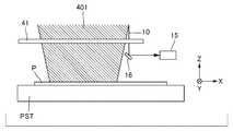
도 1은 제1 실시예에 따르는 주사 노광 장치(EE)의 구성을 도시하는 개략도이다. 주사 노광 장치(EE)는 원판(마스크)(M)을 조명하는 조명계(IL), 원판(M)을 보유 지지하는 원판 보유 지지부(MST), 평판 유리(41)를 포함하는 투영 광학계(PO), 기판(P)을 보유 지지하는 기판 보유 지지부(PST), 계측 광원(13), 센서(수광부)(15), 구동부(보정 유닛)(42) 및 제어부(제어 유닛)(51)을 포함한다. 도면에서, XY 평면은 원판(M) 및 기판(P)의 표면을 따르는 면이고, Z 축은 XY 평면에 수직이고, Y 축은 원판(M) 및 기판(P)의 주사 방향이고, X 축은 Y 축에 직교하는 비주사 방향이다.1 is a schematic diagram showing the configuration of a scanning exposure apparatus (EE) according to the first embodiment. The scanning exposure apparatus EE includes an illumination system IL for illuminating an original plate (mask) M, a original plate holding member MST for holding a original plate M, a projection optical system PO including a
조명계(IL)는 광원(도시되지 않음) 및 조명 광학계(도시되지 않음)를 포함하고, 원판(M) 상의 조명 영역을 거의 균일한 조도로 조명한다. 광원(도시되지 않음)에 대해 예를 들어 수은 램프가 사용되고, i-선, h-선, 및 g-선 등의 수은 램프의 출력 파장의 일부가 노광 광으로서 사용된다. 조명 광학계(도시되지 않음)는 원판(M) 상에 원하는 조도 분포가 획득될 수 있도록 광원으로부터 방출되는 광을 집광한다. 원판(M)은 예를 들어 석영 유리로 제조되며, 기판(W) 상에 전사될 패턴(예를 들어, 회로 패턴)이 형성된다. 원판 보유 지지부(MST) 및 기판 보유 지지부(PST)는 각각 구동부(도시되지 않음)에 의해 동기되어 이동되고, 원판(M)의 패턴은 투영 광학계(PO)를 통해 기판(P)의 노광 영역에 전사된다(주사 노광).The illumination system IL includes a light source (not shown) and an illumination optical system (not shown), and illuminates the illumination area on the original plate M with almost uniform illumination. For example, a mercury lamp is used for a light source (not shown), and a part of the output wavelength of a mercury lamp such as i-line, h-line, and g-line is used as exposure light. An illumination optical system (not shown) condenses the light emitted from the light source so that a desired illumination distribution can be obtained on the original plate M. The original plate M is made of, for example, quartz glass, and a pattern (for example, a circuit pattern) to be transferred is formed on the substrate W. The pattern of the original plate M is transferred to the exposure area of the substrate P through the projection optical system PO by a driving unit (not shown), and the original plate holding unit MST and the substrate holding unit PST are moved in synchronism with each other by a driving unit (Scan exposure).
투영 광학계(PO)는 제1 평면 미러(M1), 제1 오목 미러(M2), 볼록 미러(M3), 제2 오목 미러(M4), 제2 평면 미러(M5) 및 평면 유리(41)를 포함한다. 원판(M)과 제1 평면 미러(M1) 사이의 광로 및 제2 평면 미러(M5)와 기판(P) 사이의 광로는 평행하다. 제1 평면 미러(M1)의 경면을 포함하는 평면과 제2 평면 미러(M5)의 경면을 포함하는 평면 사이의 각도는 90도이다. 제1 평면 미러(M1) 및 제2 평면 미러(M5)는 하나의 평면 미러로서 일체화되는 것이 바람직하고, 제1 오목 미러(M2) 및 제2 오목 미러(M4) 또한 하나의 오목 미러로서 일체화되는 것이 바람직하다.The projection optical system PO includes a first plane mirror M1, a first concave mirror M2, a convex mirror M3, a second concave mirror M4, a second plane mirror M5, . The optical path between the circular plate M and the first plane mirror M1 and the optical path between the second plane mirror M5 and the substrate P are parallel. The angle between the plane including the mirror surface of the first plane mirror M1 and the plane including the mirror plane of the second plane mirror M5 is 90 degrees. The first plane mirror M1 and the second plane mirror M5 are preferably integrated as one plane mirror and the first concave mirror M2 and the second concave mirror M4 are also integrated as one concave mirror .
계측 광원(13)은 발광 디바이스(LED 등의) 및 조명 광학계를 포함하고 계측 광(10)을 -Z 방향으로 방출한다. 센서(15)는 CMOS 센서 등의 광 검출 소자(도시되지 않음) 및 수광 광학계(도시되지 않음)를 포함하고, 계측 광(10)(계측 마크(12)의 투영 화상)을 검출(수광)한다. 제어부(51)는 센서(15)의 검출 신호에 기초하여 화상의 위치 편차를 산출하고, 구동부(42)를 제어하여 평판 유리(41)를 이동시킨다. 상세한 것은 이하에 후술한다.The
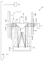
도 2는 원판 보유 지지부(MST) 및 그 근방의 구조를, 장치의 상측(+Z 방향)으로부터 본 도면이다. 원판 보유 지지부(MST)는 원판(M)의 에지를 지지함으로써 원판(M)을 보유 지지한다. 조명계(IL)는 조명 영역(202)을 조명한다. 원판 보유 지지부(MST)는 계측 광(10)이 투과하는 부분에 있어서, Y 축 방향(주사 방향)으로 연장되는 슬릿 형상의 개구(21)를 포함한다. 계측 마크(12)가 개구(21)와 조명계(IL) 사이에 설치된다. 계측 마크(12)는 노광 장치(EE)의 본체에 고정된 부재(11)에 설치된다. 계측 마크(12)는 계측 광원(13)으로부터 방출된 계측 광(10)을 조사한다.Fig. 2 is a diagram showing the structure of the disk holding portion MST and its vicinity, viewed from the upper side (+ Z direction) of the apparatus. The disk holding portion (MST) holds the disk (M) by supporting the edge of the disk (M). The illumination system IL illuminates the
도 3은 도 2의 일점 쇄선(200)을 따르는 단면도이다. 계측 광원(13)으로부터 방출된 계측 광(10)은 미러(14)에 의해 편향되고, 계측 마크(12) 및 개구(21)를 통과한다. 개구(21)는 원판 보유 지지부(MST)의 Y 축 방향으로 연장하고, 원판 스테이지(MST)를 Y 방향으로 주사하여 노광하는 동안 계측 광(10)은 항상 차단되지 않고서 원판 스테이지(MST)를 통과한다. 계측 광(10)이 통과하는 위치가 투명한 경우, 개구(21)는 요구되지 않는다. 미러(14)는 평판 미러이며, 노광을 방해하지 않도록 노광 광이 통과하는 영역(301)의 외부(광로 외부)에 배치된다. 유사하게, 계측 마크(12)(부재(11))는 노광 광의 광로 외부에 배치된다. 계측 광원(13) 및 미러(14)는 계측 마크(12)가 보유 지지 기구(도시되지 않음)에 의해 이에 고정되는 구조체, 즉, 부재(11)에 각각 고정된다.3 is a sectional view along the one-
도 4는 기판 보유 지지부(PST) 및 그 근방의 구조를 도시하는 도면이다. 계측 광원(13)으로부터 방출되어 개구(21), 계측 마크(12), 및 투영 광학계(PO)를 통과한 계측 광(10)은 미러(16)에 의해 편향되어 센서(15)에 진입한다. 센서(15)의 검출면 및 계측 마크(12)는 광학적으로 공액인 위치에 배열되고, 계측 마크(12)의 화상은 투영 광학계(PO)를 통해 센서(15) 상에 형성된다. 미러(16)는 평면 미러이며, 노광 시 노광 광이 통과하는 영역(401)의 외부에 배치된다. 센서(15) 및 미러(16)는 각각 보유 지지 기구(도시되지 않음)에 의해 노광 장치(EE)의 본체에 고정된다. 투영 광학계(PO)의 배율이 -1이기 때문에, 원판(M)의 화상은 투영 광학계(PO) 통과 이후 X 방향으로 반전된다. 따라서, 본 실시예에 따르는 계측 광(10)은 투영 광학계(PO) 통과 이후, 노광 광에 대해 +X 측을 통과하여 -Z 방향으로 진행한다.4 is a view showing the structure of the substrate holding portion (PST) and the vicinity thereof. The
제어부(51)는 계측 마크(12)의 투영 화상에 기초하여 계측 마크(12)에 대한 위치 정보를 산출하고, 산출 결과와 미리 정해진 위치 정보(기준 위치)를 비교하여 편차(차분)를 획득한다. 미리 정해진 위치 정보는 센서(15)가 이에 고정되는 위치의 좌표 등이다. 제어부(51)는 편차가 감소되도록 제어를 행하는 제어 신호를 구동부(42)에 송신한다. 구동부(42)는 제어 신호에 기초하여, 평판 유리의 XY 평면에 대한 각도(Z 축 방향에 대한 기울기)를 변경한다. 이에 의해, 계측 광(10)의 광로가 변경되고, 센서(15)에 의해 검출되는 계측 마크(12)의 화상의 위치가 보정된다.The
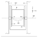
상기 기준 위치를 사용하지 않고 계측 마크(12)의 화상의 위치 변화량을 검출하는 방법이 후술된다. 도 5는 미러(16)와 센서(15) 사이에 배열되는 계측 마크(701)를 추가로 구비하는 장치의 구성을 도시한다. 계측 마크(701) 및 계측 마크(12)는 광학적으로 공액인 위치에 배열된다. 센서(15)는 계측 마크(12)의 화상과 계측 마크(701) 사이의 상대적 위치 관계를 검출함으로써 광학 화상 위치의 편차를 계측할 수 있다. 이 경우, 센서(15), 미러(16), 및 계측 마크(701)는 동일한 구조체(노광 장치(EE)의 본체 등)에 고정되는 것이 바람직하다.A method of detecting the positional change amount of the image of the
투영 광학계(PO)에 포함되는 광학 요소의 위치 편차에 의해 발생되는 계측 마크(12)의 화상의 위치 편차 및 원판(M)의 화상의 위치 편차는, 계측 마크(12)의 화상 및 원판(M)(패턴)의 화상이 투영 광학계(PO)를 통해 형성되기 때문에 동일하다. 따라서, 계측 마크(12)의 위치 편차를 보정함으로써, 기판(P) 상의 원판(M)의 위치 편차가 보정될 수 있다. 원판 보유 지지부(MST)가 스캔되는 동안 측광(10)이 센서(15)에 일정하게 진입하기 때문에 주사 노광 중 위치 편차의 변동(광학 화상의 진동)이 실시간으로 보정될 수 있다.The positional deviation of the image of the
위치 편차의 변동은 평판 유리(41)의 틸팅에 추가로 또는 틸팅 대신 기판 보유 지지부(PST) 및/또는 원판 보유 지지부(MST)의 위치를 제어함으로써 보정될 수 있다. 상술된 바와 같이 계측 마크(12) 검출과 관련된 각 요소(부재(11), 센서(15) 등)가 일체화되는 것은 위치 편차 요인(진동 등)을 각 요소에서 동일하게 하기 위해서이다. 따라서, 이 효과가 획득되는 경우, 본 발명은 상기 실시예로 한정되지 않는다.The variation of the positional deviation can be corrected by controlling the position of the substrate holding portion (PST) and / or the disk holding portion (MST) in addition to or in addition to the tilting of the flat glass (41). The reason why the respective elements (the
상술된 바와 같이, 본 실시예에 따르면, 선폭 균일성을 향상시키는데 유리한 노광 장치가 제공될 수 있다.As described above, according to this embodiment, an exposure apparatus which is advantageous for improving the line width uniformity can be provided.
(제2 실시예)(Second Embodiment)
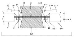
제1 실시예에서, 계측 마크는 조명계(IL)와 원판(M) 사이에서 한 곳에만 설치된다. 제2 실시예의 특징은 복수의 위치에 계측 마크를 설치하는 것이다. 도 6은 제2 실시예에 따르는 주사 노광 장치(EE)의 구성을 도시하는 개략도이다. 제1 실시예와 본 실시예의 상이한 점은, 본 실시예가 계측 광(510)을 방출하는 계측 광원(513), 계측 광원(513)을 검출하는 센서(513), 및 구동부(43)를 구비한다는 점이다.In the first embodiment, the measurement mark is installed in only one place between the illumination system IL and the circular plate M. A feature of the second embodiment is that measurement marks are provided at a plurality of positions. 6 is a schematic diagram showing the configuration of the scanning exposure apparatus (EE) according to the second embodiment. The difference between the first embodiment and the present embodiment is that the present embodiment has a measuring
도 7은 본 실시예에 따르는 원판 보유 지지부(MST) 및 그 근방의 구조를, 장치의 상측(+Z 축 방향)으로부터 본 도면이다. 제1 실시예와 본 실시예의 상이한 점은, 본 실시예가 원판 보유 지지부(MST) 상에 Y 축과 평행하게 연장하는 슬릿 형상의 개구(23)를 구비하는 점이다. 개구(23) 및 개구(21)는 광축을 포함하는 YZ 평면에 대해 대칭으로 설치되는 것이 바람직하다. 또한, 노광 장치(EE)의 본체에 고정된 베이스(511) 상에 설치되는 계측 마크(512)는 개구(23)와 조명계(IL) 사이에 위치 설정된다. 이들 추가 요소는 제1 실시예와 유사하게 보유 지지 기구(도시되지 않음)에 의해 고정된다.Fig. 7 is a diagram showing the structure of the disk holding member MST according to the present embodiment and the structure in the vicinity thereof, viewed from the upper side (+ Z-axis direction) of the apparatus. The difference between the first embodiment and this embodiment is that this embodiment has a slit-shaped
도 8은 도 7의 일점 쇄선(500)을 따르는 단면도이다. 제1 실시예와 본 실시예의 상이한 점은, 본 실시예가 베이스(511), 계측 마크(512), 계측 광원(513), 및 미러(514)를 구비하는 점이다. 이들 요소는, 원판(M)을 개재한 YZ 평면에 대해, 부재(11), 계측 마크(12), 계측 광원(13), 및 미러(14)와 대칭으로 설치되는 것이 바람직하다. 계측 광원(513)으로부터 방출된 계측 광(510)은 제1 실시예의 계측 광과 유사하게 진행한다. 이들 추가적 요소는 제1 실시예의 것과 유사한 보유 지지 기구(도시되지 않음)에 의해 고정된다.8 is a sectional view along the one-
도 9는 기판 보유 지지부(PST) 및 그 근방의 구조의 도면이다. 제1 실시예와 본 실시예의 상이한 점은, 본 실시예가 센서(515) 및 미러(516)를 구비하는 점이다. 이들 요소는 YZ 평면에 대해 센서(15) 및 미러(16)와 대칭으로 설치되는 것이 바람직하다. 상기 구성에서, 계측 마크의 화상의 회전 성분은 2개의 계측 마크의 위치 편차를 검출함으로써 검출될 수 있다. 계측 마크의 화상의 회전 성분은 2개의 계측 마크에서의 위치 편차의 차이로서 검출된다.9 is a view showing the structure of the substrate holding portion (PST) and the vicinity thereof. The difference between the first embodiment and this embodiment is that the present embodiment includes the
2개의 계측 위치에서의 위치 편차의 차이(회전 성분)는 평판 유리(41)를 이동시키는 것에 의해 보정될 수 없다. 제어부(51)는 미러(M1) 및 미러(M5)를 Z 축 주위로 회전시키도록 구동부(43)를 제어함으로써 보정을 수행한다. 상술된 바와 같이, 본 실시예는 제1 실시예와 동일한 효과를 제공한다.The difference (rotational component) of the positional deviation at the two measurement positions can not be corrected by moving the
(물품 제조 방법)(Article manufacturing method)
본 발명의 실시예에 따르는 물품 제조 방법은 반도체 디바이스 등의 마이크로 디바이스, 마이크로 구조를 갖는 요소 등과 같은 물품 등을 제조하는데 바람직하다. 물품 제조 방법은 상기 언급된 노광 장치를 사용하여 물체 상에 잠상 패턴을 형성하는 단계(예를 들어, 노광 공정), 및 이전 단계에서 잠상 패턴이 그 위에 형성된 물체를 현상하는 단계를 포함한다. 또한, 물품 제조 방법은 다른 공지된 단계(산화, 막 형성, 증착, 도핑, 평탄화, 에칭, 레지스트 박리, 다이싱, 본딩, 및 패키징 등)을 포함할 수 있다. 본 실시예에 따르는 디바이스 제조 방법은 종래의 디바이스 제조 방법에 비해, 성능, 품질, 생산성 및 디바이스의 제조 비용 중 적어도 하나에 있어서 이점을 갖는다.The article manufacturing method according to the embodiment of the present invention is preferable for manufacturing an article such as a micro device such as a semiconductor device, an element having a micro structure, or the like. The article manufacturing method includes a step (for example, an exposure step) of forming a latent image pattern on an object using the above-mentioned exposure apparatus, and a step of developing an object on which the latent image pattern is formed in the previous step. The article manufacturing method may also include other known steps (oxidation, film formation, deposition, doping, planarization, etching, resist stripping, dicing, bonding, and packaging, etc.). The device manufacturing method according to the present embodiment has an advantage over at least one of performance, quality, productivity, and device manufacturing cost as compared with the conventional device manufacturing method.
본 발명은 예시적인 실시예를 참조하여 설명되었으나, 본 발명의 양태는 개시된 예시적인 실시예로 한정되지 않는 점이 이해된다. 이하의 청구항의 범위는 그러한 변경예 및 등가적 구조예 및 기능예 모두를 포함하도록 가장 광의의 해석에 따라야 한다.While the present invention has been described with reference to exemplary embodiments, it is to be understood that the embodiments of the invention are not limited to the disclosed exemplary embodiments. The scope of the following claims should be accorded the broadest interpretation so as to encompass all such modifications and equivalent structural examples and functional examples.
본 출원은 그 전체가 여기에 참조로 통합된, 2015년 10월 6일 출원된 일본 특허 출원 번호 제2015-198420호의 우선권을 주장한다.This application claims priority from Japanese Patent Application No. 2015-198420, filed October 6, 2015, the entirety of which is incorporated herein by reference.
Claims (9)
계측 광으로 마크를 조사하도록 구성되는 계측 광원,
상기 투영 광학계를 개재하여 상기 마크의 투영 화상을 수광하도록 구성되는 수광부, 및
제어 유닛으로서, 상기 수광부 상에 수광된 상기 투영 화상에 기초하여 상기 마크의 위치 정보를 산출하고 산출된 위치 정보에 기초하여 보정을 수행하도록 구성된 보정 유닛을 제어하도록 구성되는, 제어 유닛을 포함하고,
상기 마크는 상기 마스크 상에 조명되는 노광 광의 광로 외부에 배치되는, 노광 장치.An exposure optical system configured to illuminate a mask with exposure light, and a projection optical system configured to project a pattern of the mask onto a substrate, the exposure apparatus performing scan exposure of the substrate while moving the substrate and the mask,
A measurement light source configured to irradiate the mark with measurement light,
A light receiving portion configured to receive a projected image of the mark via the projection optical system,
And a control unit configured to calculate a positional information of the mark based on the projection image received on the light receiving unit and to control a correction unit configured to perform correction based on the calculated positional information,
Wherein the mark is disposed outside the light path of the exposure light illuminated on the mask.
상기 계측 광이 통과하는 영역은 상기 마스크를 보유 지지하도록 구성된 원판 보유 지지부 상의 상기 기판의 주사 방향으로 연장하는, 노광 장치.The method according to claim 1,
And an area through which the measurement light passes extends in the scanning direction of the substrate on the disk holding member configured to hold the mask.
상기 수광부 및 상기 마크가 설치된 부재는 공통의 구조체에 고정되는, 노광 장치.The method according to claim 1,
Wherein the light receiving unit and the member provided with the mark are fixed to a common structure.
제2 마크를 제2 계측 광으로 조사하도록 구성되는 제2 계측 광원, 및
상기 투영 광학계를 개재하여 상기 제2 마크의 제2 투영 화상을 수광하도록 구성되는 제2 수광부를 포함하고,
상기 제어 유닛은 상기 제2 투영 화상에 기초하여 상기 보정 유닛을 제어하도록 구성되고,
상기 제2 마크는 상기 노광 광 및 상기 계측 광의 광로 외부에 배치되는, 노광 장치.The method according to claim 1,
A second measurement light source configured to irradiate the second mark with the second measurement light, and
And a second light receiving portion configured to receive a second projected image of the second mark via the projection optical system,
Wherein the control unit is configured to control the correction unit based on the second projection image,
And the second mark is disposed outside the light path of the exposure light and the measurement light.
상기 제2 계측 광이 통과하는 영역은 상기 마스크를 보유 지지하도록 구성된 원판 보유 지지부 상의 상기 기판의 주사 방향으로 연장하는, 노광 장치.5. The method of claim 4,
And an area through which the second measurement light passes extends in the scanning direction of the substrate on the disk holding member configured to hold the mask.
상기 마크가 설치된 부재, 상기 수광부, 상기 제2 마크가 설치된 제2 부재, 및 상기 제2 수광부는 공통의 구조체에 고정되는, 노광 장치.5. The method of claim 4,
Wherein the member provided with the mark, the light receiving unit, the second member provided with the second mark, and the second light receiving unit are fixed to a common structure.
상기 보정 유닛은 상기 투영 광학계에 포함되는 광학 부재, 상기 마스크를 보유 지지하도록 구성된 원판 보유 지지부 및 상기 기판을 보유 지지하도록 구성된 기판 보유 지지부 중 하나 이상을 구동하도록 구성된 구동부인, 노광 장치.7. The method according to any one of claims 1 to 6,
Wherein the correction unit is a drive unit configured to drive at least one of an optical member included in the projection optical system, a disk holding unit configured to hold the mask, and a substrate holding unit configured to hold the substrate.
상기 주사 노광 중에 상기 노광 광과 상이한 광으로 조사된 마크의 투영 화상을 수광하는 단계,
상기 투영 화상에 기초하여 상기 마크의 위치 정보를 산출하고 산출된 위치 정보에 기초하여 보정을 수행하도록 구성된 보정 유닛을 제어하는 단계를 포함하는, 노광 방법.An exposure method for performing a scan exposure of a substrate while moving the substrate and a mask using a projection optical system configured to project a pattern of a mask irradiated with exposure light onto a substrate,
Receiving a projected image of a mark irradiated with light different from the exposure light during the scan exposure,
And calculating a positional information of the mark based on the projection image and controlling a correction unit configured to perform correction based on the calculated positional information.
노광 광으로 조사된 마스크의 패턴을 기판 상에 투영하도록 구성된 투영 광학계를 사용하여 상기 기판 및 마스크를 이동시키면서 주사 노광을 수행하는 단계, 및
노광된 상기 기판을 현상하는 단계를 포함하고,
상기 주사 노광은,
상기 투영 광학계를 개재하여 상기 노광 광과 상이한 광으로 조사된 마크의 투영 화상을 수광하는 단계, 및
상기 투영 화상에 기초하여 상기 마크의 위치 정보를 산출하고 산출된 위치 정보에 기초하여 보정을 수행하도록 구성된 보정 유닛을 제어하는 단계를 포함하는, 물품의 제조 방법.A method of manufacturing an article,
Performing scan exposure while moving the substrate and the mask using a projection optical system configured to project a pattern of the mask irradiated with exposure light onto the substrate, and
And developing the exposed substrate,
The scan exposure may include:
Receiving a projected image of a mark irradiated with light different from the exposure light via the projection optical system; and
And controlling a correction unit configured to calculate positional information of the mark based on the projection image and to perform correction based on the calculated positional information.
Applications Claiming Priority (2)
| Application Number | Priority Date | Filing Date | Title |
|---|---|---|---|
| JPJP-P-2015-198420 | 2015-10-06 | ||
| JP2015198420A JP2017072678A (en) | 2015-10-06 | 2015-10-06 | Exposure equipment, exposure method, and manufacturing method of article |
Publications (1)
| Publication Number | Publication Date |
|---|---|
| KR20170041145A true KR20170041145A (en) | 2017-04-14 |
Family
ID=58485736
Family Applications (1)
| Application Number | Title | Priority Date | Filing Date |
|---|---|---|---|
| KR1020160128189A KR20170041145A (en) | 2015-10-06 | 2016-10-05 | Exposure apparatus, exposure method, and method of manufacturing devices |
Country Status (4)
| Country | Link |
|---|---|
| JP (1) | JP2017072678A (en) |
| KR (1) | KR20170041145A (en) |
| CN (1) | CN106560745A (en) |
| TW (1) | TWI655511B (en) |
Families Citing this family (1)
| Publication number | Priority date | Publication date | Assignee | Title |
|---|---|---|---|---|
| JP7453790B2 (en) * | 2020-01-15 | 2024-03-21 | キヤノン株式会社 | Exposure device and article manufacturing method |
Family Cites Families (8)
| Publication number | Priority date | Publication date | Assignee | Title |
|---|---|---|---|---|
| FR2704660B1 (en) * | 1993-04-27 | 1995-07-13 | Sgs Thomson Microelectronics | Masks for a double-sided exposure machine. |
| WO1999050712A1 (en) * | 1998-03-26 | 1999-10-07 | Nikon Corporation | Exposure method and system, photomask, method of manufacturing photomask, micro-device and method of manufacturing micro-device |
| JP5203992B2 (en) * | 2008-03-25 | 2013-06-05 | 株式会社ニューフレアテクノロジー | Electron beam drawing apparatus and electron beam drawing method |
| US20100092599A1 (en) * | 2008-10-10 | 2010-04-15 | Molecular Imprints, Inc. | Complementary Alignment Marks for Imprint Lithography |
| JP5499398B2 (en) * | 2009-05-11 | 2014-05-21 | Nskテクノロジー株式会社 | Exposure apparatus and exposure method |
| CN102156392A (en) * | 2010-02-11 | 2011-08-17 | 中芯国际集成电路制造(上海)有限公司 | Device and method for detecting alignment parameter of photoetching machine |
| NL2005996A (en) * | 2010-02-19 | 2011-08-22 | Asml Netherlands Bv | Lithographic apparatus and device manufacturing method. |
| JP5933289B2 (en) * | 2012-02-23 | 2016-06-08 | 三菱電機株式会社 | SOI wafer and manufacturing method thereof |
-
2015
- 2015-10-06 JP JP2015198420A patent/JP2017072678A/en active Pending
-
2016
- 2016-09-22 TW TW105130643A patent/TWI655511B/en active
- 2016-09-30 CN CN201610870966.XA patent/CN106560745A/en active Pending
- 2016-10-05 KR KR1020160128189A patent/KR20170041145A/en not_active Application Discontinuation
Also Published As
| Publication number | Publication date |
|---|---|
| JP2017072678A (en) | 2017-04-13 |
| TWI655511B (en) | 2019-04-01 |
| TW201714024A (en) | 2017-04-16 |
| CN106560745A (en) | 2017-04-12 |
Similar Documents
| Publication | Publication Date | Title |
|---|---|---|
| KR101444981B1 (en) | Exposure apparatus, exposure method, and method of manufacturing device | |
| KR100365602B1 (en) | Exposure Method and Apparatus and Semiconductor Device Manufacturing Method | |
| JP5507875B2 (en) | Exposure apparatus, exposure method, and device manufacturing method | |
| JPH1145846A (en) | Scanning type exposure method and aligner | |
| US7474381B2 (en) | Exposure apparatus and device manufacturing method | |
| KR20090089820A (en) | Exposure apparatus and device manufacturing method | |
| US10488764B2 (en) | Lithography apparatus, lithography method, and method of manufacturing article | |
| US20100103393A1 (en) | Scanning exposure apparatus and device manufacturing method | |
| KR20170041145A (en) | Exposure apparatus, exposure method, and method of manufacturing devices | |
| JPH11307436A (en) | Projection aligner, reticle and reticle aligning method | |
| JP6139870B2 (en) | Exposure method, exposure apparatus, and article manufacturing method | |
| CN107305320B (en) | Detection device, detection method, program, lithographic apparatus, and article manufacturing method | |
| JP5773735B2 (en) | Exposure apparatus and device manufacturing method | |
| US7733498B2 (en) | Exposure apparatus, method of controlling the same, and manufacturing method | |
| JPH09115820A (en) | Scanning projection aligner and aligning method | |
| JPH1187233A (en) | Projection aligner | |
| US8237917B2 (en) | Exposure apparatus and device manufacturing method | |
| JP2000021711A (en) | Aligner and method for detecting its focal point | |
| JP6929041B2 (en) | Exposure equipment and manufacturing method of articles | |
| JP6053316B2 (en) | Lithographic apparatus and article manufacturing method | |
| JP2010251409A (en) | Exposure method, exposure apparatus, and device manufacturing method | |
| WO1999005707A1 (en) | Focusing method, exposure method, and aligner | |
| TW200923589A (en) | Positioning apparatus, exposure apparatus, and device manufacturing method | |
| JP2009170664A (en) | Surface position detector, aligner, and device manufacturing method | |
| JP2002043211A (en) | Aligner and exposure system |
Legal Events
| Date | Code | Title | Description |
|---|---|---|---|
| A201 | Request for examination | ||
| E902 | Notification of reason for refusal | ||
| WITB | Written withdrawal of application |