JP7453790B2 - Exposure device and article manufacturing method - Google Patents
Exposure device and article manufacturing method Download PDFInfo
- Publication number
- JP7453790B2 JP7453790B2 JP2020004671A JP2020004671A JP7453790B2 JP 7453790 B2 JP7453790 B2 JP 7453790B2 JP 2020004671 A JP2020004671 A JP 2020004671A JP 2020004671 A JP2020004671 A JP 2020004671A JP 7453790 B2 JP7453790 B2 JP 7453790B2
- Authority
- JP
- Japan
- Prior art keywords
- light
- optical system
- measurement
- projection optical
- exposure
- Prior art date
- Legal status (The legal status is an assumption and is not a legal conclusion. Google has not performed a legal analysis and makes no representation as to the accuracy of the status listed.)
- Active
Links
- 238000004519 manufacturing process Methods 0.000 title claims description 13
- 230000003287 optical effect Effects 0.000 claims description 324
- 238000005259 measurement Methods 0.000 claims description 222
- 239000000758 substrate Substances 0.000 claims description 121
- 238000001514 detection method Methods 0.000 claims description 56
- 238000000034 method Methods 0.000 claims description 29
- 230000008859 change Effects 0.000 claims description 9
- 238000003384 imaging method Methods 0.000 claims description 5
- 238000010586 diagram Methods 0.000 description 10
- 238000006243 chemical reaction Methods 0.000 description 9
- 238000005286 illumination Methods 0.000 description 8
- 238000012545 processing Methods 0.000 description 8
- 238000004458 analytical method Methods 0.000 description 7
- 239000004065 semiconductor Substances 0.000 description 7
- 230000001133 acceleration Effects 0.000 description 6
- 230000007423 decrease Effects 0.000 description 6
- 230000007246 mechanism Effects 0.000 description 6
- 230000008569 process Effects 0.000 description 6
- 238000012546 transfer Methods 0.000 description 5
- 238000004364 calculation method Methods 0.000 description 4
- 238000012937 correction Methods 0.000 description 3
- 230000000875 corresponding effect Effects 0.000 description 3
- 230000004907 flux Effects 0.000 description 3
- 230000035945 sensitivity Effects 0.000 description 3
- 230000003321 amplification Effects 0.000 description 2
- 239000003795 chemical substances by application Substances 0.000 description 2
- 230000008021 deposition Effects 0.000 description 2
- 230000000694 effects Effects 0.000 description 2
- 238000001914 filtration Methods 0.000 description 2
- 239000011521 glass Substances 0.000 description 2
- 238000009434 installation Methods 0.000 description 2
- 239000004973 liquid crystal related substance Substances 0.000 description 2
- 238000001459 lithography Methods 0.000 description 2
- 239000000463 material Substances 0.000 description 2
- 238000012986 modification Methods 0.000 description 2
- 230000004048 modification Effects 0.000 description 2
- 238000003199 nucleic acid amplification method Methods 0.000 description 2
- 238000004088 simulation Methods 0.000 description 2
- 238000013519 translation Methods 0.000 description 2
- 230000007723 transport mechanism Effects 0.000 description 2
- 238000012935 Averaging Methods 0.000 description 1
- 101100269850 Caenorhabditis elegans mask-1 gene Proteins 0.000 description 1
- VYZAMTAEIAYCRO-UHFFFAOYSA-N Chromium Chemical compound [Cr] VYZAMTAEIAYCRO-UHFFFAOYSA-N 0.000 description 1
- 238000005452 bending Methods 0.000 description 1
- 230000000903 blocking effect Effects 0.000 description 1
- 229910052804 chromium Inorganic materials 0.000 description 1
- 239000011651 chromium Substances 0.000 description 1
- 238000007796 conventional method Methods 0.000 description 1
- 230000002596 correlated effect Effects 0.000 description 1
- 238000013461 design Methods 0.000 description 1
- 230000006866 deterioration Effects 0.000 description 1
- 238000011161 development Methods 0.000 description 1
- 230000005672 electromagnetic field Effects 0.000 description 1
- 238000005530 etching Methods 0.000 description 1
- 238000002474 experimental method Methods 0.000 description 1
- 239000004615 ingredient Substances 0.000 description 1
- 238000007689 inspection Methods 0.000 description 1
- QSHDDOUJBYECFT-UHFFFAOYSA-N mercury Chemical compound [Hg] QSHDDOUJBYECFT-UHFFFAOYSA-N 0.000 description 1
- 229910052753 mercury Inorganic materials 0.000 description 1
- 230000003647 oxidation Effects 0.000 description 1
- 238000007254 oxidation reaction Methods 0.000 description 1
- 238000004806 packaging method and process Methods 0.000 description 1
- 210000001747 pupil Anatomy 0.000 description 1
- 230000009466 transformation Effects 0.000 description 1
- 238000002834 transmittance Methods 0.000 description 1
- 230000032258 transport Effects 0.000 description 1
Images


Classifications
-
- G—PHYSICS
- G03—PHOTOGRAPHY; CINEMATOGRAPHY; ANALOGOUS TECHNIQUES USING WAVES OTHER THAN OPTICAL WAVES; ELECTROGRAPHY; HOLOGRAPHY
- G03F—PHOTOMECHANICAL PRODUCTION OF TEXTURED OR PATTERNED SURFACES, e.g. FOR PRINTING, FOR PROCESSING OF SEMICONDUCTOR DEVICES; MATERIALS THEREFOR; ORIGINALS THEREFOR; APPARATUS SPECIALLY ADAPTED THEREFOR
- G03F7/00—Photomechanical, e.g. photolithographic, production of textured or patterned surfaces, e.g. printing surfaces; Materials therefor, e.g. comprising photoresists; Apparatus specially adapted therefor
- G03F7/20—Exposure; Apparatus therefor
-
- G—PHYSICS
- G03—PHOTOGRAPHY; CINEMATOGRAPHY; ANALOGOUS TECHNIQUES USING WAVES OTHER THAN OPTICAL WAVES; ELECTROGRAPHY; HOLOGRAPHY
- G03F—PHOTOMECHANICAL PRODUCTION OF TEXTURED OR PATTERNED SURFACES, e.g. FOR PRINTING, FOR PROCESSING OF SEMICONDUCTOR DEVICES; MATERIALS THEREFOR; ORIGINALS THEREFOR; APPARATUS SPECIALLY ADAPTED THEREFOR
- G03F7/00—Photomechanical, e.g. photolithographic, production of textured or patterned surfaces, e.g. printing surfaces; Materials therefor, e.g. comprising photoresists; Apparatus specially adapted therefor
- G03F7/70—Microphotolithographic exposure; Apparatus therefor
- G03F7/708—Construction of apparatus, e.g. environment aspects, hygiene aspects or materials
- G03F7/7085—Detection arrangement, e.g. detectors of apparatus alignment possibly mounted on wafers, exposure dose, photo-cleaning flux, stray light, thermal load
-
- G—PHYSICS
- G03—PHOTOGRAPHY; CINEMATOGRAPHY; ANALOGOUS TECHNIQUES USING WAVES OTHER THAN OPTICAL WAVES; ELECTROGRAPHY; HOLOGRAPHY
- G03F—PHOTOMECHANICAL PRODUCTION OF TEXTURED OR PATTERNED SURFACES, e.g. FOR PRINTING, FOR PROCESSING OF SEMICONDUCTOR DEVICES; MATERIALS THEREFOR; ORIGINALS THEREFOR; APPARATUS SPECIALLY ADAPTED THEREFOR
- G03F7/00—Photomechanical, e.g. photolithographic, production of textured or patterned surfaces, e.g. printing surfaces; Materials therefor, e.g. comprising photoresists; Apparatus specially adapted therefor
- G03F7/70—Microphotolithographic exposure; Apparatus therefor
- G03F7/70483—Information management; Active and passive control; Testing; Wafer monitoring, e.g. pattern monitoring
- G03F7/7055—Exposure light control in all parts of the microlithographic apparatus, e.g. pulse length control or light interruption
Description
本発明は、露光装置、および物品の製造方法に関する。 The present invention relates to an exposure apparatus and a method of manufacturing an article.
半導体デバイスや液晶ディスプレイなどの製造工程の1つであるリソグラフィ工程では、投影光学系を介して原版のパターン像を基板上に投影することで基板を露光する露光装置が使用される。露光装置では、例えば半導体デバイス等の微細化に伴い、原版のパターンを基板上に精度よく転写することが求められているが、基板の露光中における投影光学系の光学特性の変化が転写精度を低下させる1つの要因となりうる。投影光学系の光学特性の変化は、例えば、投影光学系に含まれる光学素子の振動、投影光学系内の温度変化や圧力変化などによって引き起こされうる。特許文献1には、原版の近傍に計測マークを配置し、投影光学系による計測マークの投影像を受光部で受光することで得られる当該投影像の位置に基づいて、投影光学系の光学特性(結像性能)を補正する構成が開示されている。 In a lithography process, which is one of the manufacturing processes for semiconductor devices, liquid crystal displays, etc., an exposure apparatus is used that exposes a substrate by projecting a pattern image of an original onto the substrate via a projection optical system. With the miniaturization of semiconductor devices, for example, exposure equipment is required to accurately transfer the pattern of the original onto the substrate, but changes in the optical characteristics of the projection optical system during exposure of the substrate affect the transfer accuracy. This could be one factor that causes the decline. Changes in the optical characteristics of the projection optical system can be caused by, for example, vibrations of optical elements included in the projection optical system, temperature changes and pressure changes within the projection optical system. Patent Document 1 discloses that a measurement mark is placed near the original, and the optical characteristics of the projection optical system are determined based on the position of the projection image obtained by receiving the projection image of the measurement mark by the projection optical system with a light receiving section. A configuration for correcting (imaging performance) is disclosed.
特許文献1に記載された構成では、計測マークは、露光装置の本体に固定された部材に設けられており、計測マークの投影像を受光する受光部は、計測マークと同一の構造体(露光装置の本体)に固定されている。つまり、投影光学系と受光部とが離間して設けられている。しかしながら、このような構成では、投影光学系と受光部との相対位置が変動することがあるため、受光部による計測マークの投影像の受光結果に基づいて、投影光学系の光学特性を精度よく計測することが困難になりうる。 In the configuration described in Patent Document 1, the measurement mark is provided on a member fixed to the main body of the exposure apparatus, and the light receiving section that receives the projected image of the measurement mark is attached to the same structure as the measurement mark (exposure (main body of the device). In other words, the projection optical system and the light receiving section are provided apart from each other. However, in such a configuration, the relative position between the projection optical system and the light receiving section may fluctuate, so the optical characteristics of the projection optical system are accurately determined based on the reception result of the projected image of the measurement mark by the light receiving section. Can be difficult to measure.
そこで、本発明は、投影光学系の光学特性を精度よく計測するために有利な技術を提供することを目的とする。 Therefore, an object of the present invention is to provide an advantageous technique for accurately measuring the optical characteristics of a projection optical system.
上記目的を達成するために、本発明の一側面としての露光装置は、基板を露光する露光装置であって、複数の光学素子を含み、露光光により原版のパターン像を前記基板に投影する投影光学系と、前記露光光が経由する前記投影光学系の光学素子を経由して前記投影光学系から射出された計測光を用いて、前記投影光学系の光学特性を計測する計測部と、前記計測部での計測結果に基づいて、前記基板上での前記露光光の照射位置を補正する制御部と、を含み、前記計測部は、前記計測光を受光する受光素子を含み、前記制御部は、前記受光素子上での前記計測光の位置変動の周波数成分に基づいて、前記複数の光学素子の中から、前記露光光の位置変動に影響を与えている光学素子を特定し、特定した光学素子を駆動することにより前記基板上での前記露光光の照射位置を補正する、ことを特徴とする。 In order to achieve the above object, an exposure apparatus as one aspect of the present invention is an exposure apparatus that exposes a substrate, includes a plurality of optical elements, and projects a pattern image of an original onto the substrate using exposure light. an optical system; a measurement unit that measures optical characteristics of the projection optical system using measurement light emitted from the projection optical system via an optical element of the projection optical system through which the exposure light passes; a control unit that corrects the irradiation position of the exposure light on the substrate based on the measurement result in the measurement unit, the measurement unit includes a light receiving element that receives the measurement light, and the control unit identifies and identifies an optical element that is affecting the positional fluctuation of the exposure light from among the plurality of optical elements based on the frequency component of the positional fluctuation of the measurement light on the light receiving element. The method is characterized in that the irradiation position of the exposure light on the substrate is corrected by driving an optical element .
本発明の更なる目的又はその他の側面は、以下、添付図面を参照して説明される好ましい実施形態によって明らかにされるであろう。 Further objects or other aspects of the invention will become apparent from the preferred embodiments described below with reference to the accompanying drawings.
本発明によれば、例えば、投影光学系の光学特性を精度よく計測するために有利な技術を提供することができる。 According to the present invention, for example, it is possible to provide an advantageous technique for accurately measuring the optical characteristics of a projection optical system.
以下、添付図面を参照して実施形態を詳しく説明する。なお、以下の実施形態は特許請求の範囲に係る発明を限定するものではない。実施形態には複数の特徴が記載されているが、これらの複数の特徴の全てが発明に必須のものとは限らず、また、複数の特徴は任意に組み合わせられてもよい。さらに、添付図面においては、同一若しくは同様の構成に同一の参照番号を付し、重複した説明は省略する。 Hereinafter, embodiments will be described in detail with reference to the accompanying drawings. Note that the following embodiments do not limit the claimed invention. Although a plurality of features are described in the embodiments, not all of these features are essential to the invention, and the plurality of features may be arbitrarily combined. Furthermore, in the accompanying drawings, the same or similar components are designated by the same reference numerals, and redundant description will be omitted.
<第1実施形態>
本発明に係る第1実施形態の露光装置100について説明する。露光装置100は、半導体デバイスや液晶ディスプレイなどの製造に用いられるリソグラフィ装置である。本実施形態の露光装置100は、ステッパ方式またはスキャン方式により原版(マスク、レチクル)のパターン像を基板上に投影することで基板を露光し、原版のパターンを基板に転写する投影露光装置である。以下では、露光装置100として、スリット光により基板を走査露光するスキャン方式の露光装置を例示して説明する。
<First embodiment>
An
[露光装置の構成]
図1は、第1実施形態の露光装置100の構成を示す概略図である。本実施形態の露光装置100は、照明光学系10と、原版Mを保持して移動可能な原版ステージ20と、投影光学系30と、基板Wを保持して移動可能な基板ステージ40と、計測部50と、制御部60とを含みうる。制御部60は、例えばCPUやメモリなどを有するコンピュータによって構成され、基板Wの露光処理(露光装置100の各部)を制御する。原版Mは、基板W上に転写すべき微細なパターン(例えば回路パターン)がクロムなどの遮光材料で形成されたガラス製の原版である。また、基板Wとしては、半導体ウェハやガラスプレートなどが用いられうる。
[Exposure device configuration]
FIG. 1 is a schematic diagram showing the configuration of an
照明光学系10は、原版上で所望の照度分布が得られるように、光源(不図示)からの光を例えばY軸方向に長い円弧状の光に整形し、整形した光(スリット光)で原版Mをほぼ均一な照度で照明する。光源としては水銀ランプ等が用いられうる。原版Mおよび基板Wは、原版ステージ20および基板ステージ40によってそれぞれ保持されており、投影光学系30を介して光学的にほぼ共役な位置(投影光学系30の物体面および像面の位置)に配置される。投影光学系30は、所定の投影倍率を有し、マスク1のパターン像を複数のミラーで反射させて基板2に投影する。そして、マスクステージ20および基板ステージ40を、投影光学系30の物体面と平行な方向(例えばX軸方向)に、投影光学系30の投影倍率に応じた速度比で相対的に同期走査する。これにより、基板Wの走査露光を行い、原版Mに形成されたパターンを基板W(具体的には、基板上のレジスト(感光剤))に転写することができる。
The illumination
投影光学系30は、例えば、図1に示すように、台形ミラー31と、凹面ミラー32と、凸面ミラー33とを含むように構成されうる。照明光学系10から射出されて原版Mを通過したパターン光EL(以下では「露光光EL」と呼ぶことがある)は、台形ミラー31の上面により光路を折り曲げられ、凹面ミラー32の反射面の上部に入射する。凹面ミラー32の反射面の上部で反射した露光光ELは、凸面ミラー33の反射面で反射し、凹面ミラー32の反射面の下部に入射する。凹面ミラー32の反射面の下部で反射した露光光ELは、台形ミラー31の下面により光路を折り曲げられ、基板Wに入射する。このように構成された投影光学系30では、凸面ミラー33の反射面が光学的な瞳となる。また、投影光学系30は、原版Mと基板Wの光軸方向(Z方向)の位置変動による倍率誤差を生じないように、原版M側と基板W側、つまり物体面側、像面側共にテレセントリック光学系となっている。
The projection optical system 30 may be configured to include, for example, a
また、投影光学系30には、各光学素子を駆動するためのアクチュエータが設けられうる。具体的には、台形ミラー31を駆動するためのアクチュエータ34と、凹面ミラー32を駆動するためのアクチュエータ35と、凸面ミラー33を駆動するためのアクチュエータ36とが設けられうる。各アクチュエータ34~36は、各光学素子の変動(振動)を低減するために用いられうる。
Further, the projection optical system 30 may be provided with an actuator for driving each optical element. Specifically, an
ここで、アクチュエータ35は、凹面ミラー32に対して少なくとも3箇所に配置されることが好ましい。アクチュエータ35としては、例えば電磁アクチュエータなど、固定部と可動部とが非接触で構成されたアクチュエータを用いることができ、この場合、凹面ミラー32の支持部の干渉による凹面ミラー32への変形を回避することができる。また、この場合、熱源であるコイルを凹面ミラー32の支持部側に、非熱源である磁石を凹面ミラー32に取り付けることが望ましい。電磁アクチュエータとしては、電磁石の吸引力を用いたものを適用してもよいし、ボイスコイル型のリニアモータを適用してもよい。ボイスコイル型のリニアモータを用いる場合、駆動方向以外の他成分の力が小さくなるため、より適している。台形ミラー31に設けられるアクチュエータ34、および凸面ミラー33に設けられるアクチュエータ35についても同様であり、電磁アクチュエータを用いたり光学素子から熱源を離して配置したりすることが好ましい。また、アクチュエータ34~36としては、駆動方向以外をかわし機構で支持する手段を用いれば、圧電型やねじ送り機構を用いることも可能である。
Here, it is preferable that the
このような露光装置100では、一般に、設置床からの外乱振動を減衰させる除振装置(不図示)が設けられうるが、当該除振装置で外乱振動を消失させることは困難である。そのため、基板Wの走査露光中において、露光装置100の各部(特に投影光学系30)に外乱振動が伝達することがある。また、基板Wの走査露光中では、原版ステージ20および基板ステージ40が移動するため、その移動により生じた振動が投影光学系30に伝達することもある。これらの場合、投影光学系30に含まれる各光学素子(例えば台形ミラー31、凹面ミラー32、凸面ミラー33)が振動し、露光光ELの位置変動(振動、像ずれ)が生じうる。その結果、原版Mのパターン像を基板上に精度よく投影すること、即ち、原版Mのパターンを基板上に精度よく転写することが困難になりうる。そこで、本実施形態の露光装置100は、投影光学系30の光学特性を計測する計測部50を有し、計測部50での計測結果に基づいて基板上での露光光ELの照射位置を補正する。
Such an
計測部50は、平行光(コリメート光)としての計測光MLを投影光学系内に投光し、露光光ELが経由する投影光学系内の光学素子を経由した計測光MLに基づいて、投影光学系30の光学特性、即ち、投影光学系30の内部状態を計測する。具体的には、計測部50は、計測光ML(光ビーム)を投影光学系30内に投光する投光部51と、投影光学系30を通過して射出された計測光MLを受光する受光部52とを有する。投影光学系30内において、計測光MLは、露光光ELと同様に、台形ミラー31の上面、凹面ミラー32の反射面の上部、凸面ミラー33、凹面ミラー32の反射面の下部、台形ミラー31の下面の順番で反射されて、投影光学系30から射出される。
The
投光部51は、例えば、光源51aとミラー51bとを含みうる。光源51aは、気体レーザや半導体レーザ、LED等の発光素子とコリメータレンズとを有し、計測光MLを平行光(コリメート光)として射出する。ミラー51bは、光源51aから射出された計測光MLの光路を折り曲げて、計測光MLを投影光学系30内に導く。投光部51(光源51a、ミラー51b)は、原版ステージ20(原版M)と投影光学系30との間において投影光学系30に取り付けられている。また、投光部51は、原版Mと投影光学系30との間に配置されたミラー51bにより、計測光MLが投影光学系30の光軸に平行となるように構成されている。このようにミラー51bを原版Mの下方側に配置することにより、計測光MLを常に投影光学系30内に入射させることが可能となる。
The
受光部52は、例えば、受光素子52aとミラー52bとを含みうる。ミラー52bは、投影光学系30内を通過して投影光学系30から射出された計測光MLの光路を基板Wの前で折り曲げて、計測光MLを受光素子52aに導く。受光素子52aは、計測光MLを受光し、計測光MLの受光位置に応じた信号値を出力する。本実施形態の場合、受光素子52aは、計測光MLを受光する受光面53を有し、当該受光面53における計測光MLの受光位置に応じた信号値を出力する。受光素子52aの具体的な構成については後述する。受光部52(受光素子52a、ミラー52b)は、基板ステージ40(基板W)と投影光学系30との間において投影光学系30に取り付けられている。本実施形態の場合、投影光学系30は両側テレセントリック光学系であり、計測光MLは投影光学系30の光軸に平行に入射されるため、投影光学系30の基板W側においても計測光MLが光軸に平行に射出される。また、計測光MLとして平行光が用いられるため、受光素子52a(受光面53)を配置する位置に関して、投影光学系30の結像位置を考慮する必要がない。したがって、本実施形態の受光素子52a(受光面53)は、投影光学系30の結像位置とは異なる位置に配置されてもよい。
The
ここで、投光部51の光源51aとして半導体レーザまたはLEDを用いる場合には、計測光MLを高速に点滅させることが可能となるため、特定の周波数を有する計測光MLを射出することができる。この場合、受光部52の受光素子52aからの信号の出力周波数を、光源51aから射出される計測光MLの周波数と同期させることで、ノイズ成分を低減することができる。即ち、特定の周波数成分に着目した受光素子52aの信号値を得ることができる。
Here, when a semiconductor laser or an LED is used as the
上記のように構成された計測部50は、露光光ELに対して複数設けられうる。図2は、投影光学系30を上方(原版ステージ20側)から見た図であり、露光光ELの断面(照明領域11)と計測部50の投光部51(光源51a、ミラー51b)とが図示されている。複数の計測部50は、露光光ELの周囲における複数個所において、複数の計測光MLがそれぞれ投影光学系30内に投光されるように配置されうる。図2に示す例では、4つの計測部50が設けられており、当該4つの計測部50は、露光光EL(照明領域11)の周囲において、露光光ELの光軸(Z軸方向)を横切り且つ走査方向(X方向)に平行な直線を軸とした線対称に配置されている。このように複数の計測部50を設けることで、投影光学系30内における計測光MLの位置変動(光軸ずれ)だけでなく、投影光学系30の倍率成分も計測することができる。
A plurality of
なお、計測光MLの位置変動とは、投影光学系30を通過することにより、計測光MLの光軸が、基準位置から並進方向(XY方向)および回転方向(Z軸周りの回転方向)へ変動する(ずれる)ことをいう。また、基準位置とは、投影光学系30への入射位置に応じて投影光学系30から射出されるべき計測光MLの光軸位置のことでありうる。 Note that the positional fluctuation of the measurement light ML means that the optical axis of the measurement light ML changes from the reference position to the translation direction (XY direction) and rotation direction (rotation direction around the Z axis) by passing through the projection optical system 30. It means to fluctuate (shift). Further, the reference position may be the optical axis position of the measurement light ML to be emitted from the projection optical system 30 depending on the position of incidence on the projection optical system 30.
次に、受光部52の受光素子52aを用いた投影光学系30の光学特性の計測方法について説明する。受光素子52aとしては、例えばフォトダイオードなどの光強度センサ(光電変換センサ)が用いられうる。本実施形態の場合、受光素子52aは、受光面53における複数の部分領域の各々において光強度を検出することができるように構成された複数のフォトダイオードを含みうる。以下では、受光素子52aに4個のフォトダイオード(4分割フォトダイオードとも呼ばれる)を用いた例を説明する。
Next, a method of measuring the optical characteristics of the projection optical system 30 using the
図3は、本実施形態の受光素子52aの受光面53を示す図である。本実施形態の場合、受光面53は、図1に示すようにYZ面であるが、図3では、説明を分かり易くするため、受光部52のミラー52bを用いずに受光面53をXY面とした場合について説明する。また、図3に示す例では、受光素子52aは4分割フォトダイオードによって構成され、受光面53は、光強度を個別に検出可能な4つの部分領域53a~53dを有する。即ち、受光素子52aとしての4分割フォトダイオードは、部分領域53a~53dの各々に入射した光の光量に応じた信号値(例えば電流値)を個別に出力するように構成されている。また、4分割フォトダイオードから個別に出力された信号値(電流値)は電流電圧変換器に接続されて電圧値に変換されうる。
FIG. 3 is a diagram showing the
例えば、図3のように、計測光MLが受光面53の中央位置(4分割フォトダイオードの中央位置)に入射した場合を考える。この場合、4分割フォトダイオード部からそれぞれ4つの電圧値A、B、C、Dが得られる。この電圧値A、B、C、Dは、計測光ELの光量、フォトダイオード感度、電流電圧変換器ゲインなどに依存する。さらに、これらの電圧値は、計測光ELの位置変動によって変化し、その変化量は、計測光ELの径、形状(光量分布)に依存する。例えば、計測光ELの入射位置(受光位置)が、図3の状態から右方向(+X方向)に変動すると、受光面53の部分領域53b~53cでは受光量が増加し、受光面53の部分領域53a、53dでは受光量が減少する。つまり、電圧値B、Cは増加し、電圧値A、Dは減少することとなる。一方、計測光ELの入射位置(受光位置)が、図3の状態から上方向(+Y方向)に移動すると、受光面53の部分領域53c~53dでは受光量が増加し、受光面53の部分領域53a~53bでは受光量が減少する。つまり、電圧値C、Dは増加し、電圧値A、Bは減少することとなる。
For example, as shown in FIG. 3, consider a case where the measurement light ML is incident on the center position of the light receiving surface 53 (the center position of the four-part photodiode). In this case, four voltage values A, B, C, and D are obtained from each of the four-divided photodiode sections. These voltage values A, B, C, and D depend on the light intensity of the measurement light EL, the photodiode sensitivity, the current-voltage converter gain, and the like. Further, these voltage values change due to positional fluctuations of the measurement light EL, and the amount of change depends on the diameter and shape (light amount distribution) of the measurement light EL. For example, when the incident position (light receiving position) of the measurement light EL changes in the right direction (+X direction) from the state shown in FIG. The amount of light received decreases in the
したがって、制御部60は、4分割フォトダイオードから得られた電圧値A~Dに基づいて、受光面53の中央位置を基準としたときの計測光MLの受光位置ずれを求めることができる。受光面53における計測光MLの受光位置ずれは、投影光学系30での計測光MLの光軸ずれ(X,Y)に比例しており、以下の式(1)~(2)によって演算されうる。なお、上記の演算は、本実施形態では制御部60によって行われうるが、計測部50にCPUなどの処理部が設けられている場合には当該処理部で行われてもよい。
X=kx{-(A-C)+(B-D)} ・・・(1)
Y=ky{-(A-C)-(B-D)} ・・・(2)
Therefore, the
X=kx{-(A-C)+(BD)}...(1)
Y=ky{-(A-C)-(BD)}...(2)
式(1)の係数kxは、受光面53における計測光MLの受光位置ずれ(X方向)を投影光学系30での計測光MLの光軸ずれ(X方向)に変換するための変換係数(比例係数)である。同様に、式(2)の係数kyは、受光面53における計測光MLの受光位置ずれ(Y方向)を投影光学系30での計測光MLの光軸ずれ(Y方向)に変換するための変換係数(比例係数)である。係数kxおよび係数kyは、例えば事前の実験やシミュレーションなどによって求められうる。一例として、投影光学系30への計測光MLの入射位置を変更して、投影光学系30での計測光MLの光軸をずらしながら、受光面53での計測光MLの受光位置ずれの変化を逐次計測することにより、係数kxおよび係数kyを得ることができる。
The coefficient kx in equation (1) is a conversion coefficient ( (proportional coefficient). Similarly, the coefficient ky in equation (2) is used to convert the light receiving position deviation (Y direction) of the measurement light ML on the
また、計測光MLの径が、4分割フォトダイオードの受光面53より大きい場合や、4分割フォトダイオードの継ぎ目領域(光強度を検出できない領域)の幅を無視できない程度に小さい場合などでは、電圧値A~Dの正規化を行ってもよい。具体的には、受光面53における計測光MLの受光位置ずれによって複数の部分領域53a~53dでの受光量の総和が変動する場合には、以下の式(3)~(4)に示すように、当該受光量の総和で正規化することで、主に直線性の改善を図ることができる。なお、式(3)~(4)の係数kx’および係数ky’は、受光面53における計測光MLの受光位置ずれを投影光学系30での計測光MLの光軸ずれに変換するための変換係数(比例係数)である。
X=kx’{-(A-C)+(B-D)}/(A+B+C+D) ・・・(3)
Y=ky’{-(A-C)-(B-D)}/(A+B+C+D) ・・・(4)
In addition, when the diameter of the measurement light ML is larger than the
X=kx'{-(A-C)+(B-D)}/(A+B+C+D)...(3)
Y=ky'{-(A-C)-(B-D)}/(A+B+C+D)...(4)
ここで、計測光MLは、投影光学系30内において露光光ELが経由した複数の光学素子を経由している。そのため、受光面53における計測光MLの受光位置ずれから演算される投影光学系30での計測光MLの光軸ずれを、基板上での露光光ELの位置変動(像ずれ)に対応させることができる。つまり、制御部60は、上記の演算を行うことにより、受光素子52a(受光面53)における計測光MLの受光位置に基づいて、投影光学系30での露光光ELの位置変動を推定することができる。そして、推定された露光光ELの位置変動に応じて、基板上での露光光ELの照射位置を補正することができる。本実施形態の場合、基板上での露光光ELの照射位置の補正を、基板Wの走査露光と並行して行うことができる。
Here, the measurement light ML passes through a plurality of optical elements within the projection optical system 30 through which the exposure light EL passes. Therefore, the optical axis shift of the measurement light ML in the projection optical system 30, which is calculated from the light reception position shift of the measurement light ML on the
このように、本実施形態の露光装置100では、平行光である計測光MLを用いることにより、受光素子52aとして複数のフォトダイオード(例えば4分割フォトダイオード)を適用することができる。つまり、本実施形態の構成では、特許文献1に記載されたようにCMOSセンサ等の光検出素子および受光光学系から構成された画像センサを用いてマークの投影像を検出する従来の構成に比べ、簡素な構成で投影光学系30の光学特性を計測することができる。また、本実施形態の構成では、投影光学系30の光学特性の計測にマークの投影像を用いないため、投影光学系30の結像位置を考慮せずに、受光素子52aの受光面53を任意に配置することができる。即ち、投影光学系30の結像位置とは異なる位置に受光面53を配置することができる。そのため、装置コストや装置の設計自由度の点で有利になる。また、本実施形態の構成では、フォトダイオードを用いており、マークの投影像の位置を演算する従来の構成と比べて演算規模が小さいため、投影光学系30の光学特性の計測周期を短くすることができる。つまり、従来の構成では、投影光学系30の光学特性を離散的に計測しているのに対し、本実施形態の構成では、投影光学系30の光学特性を連続的に計測することができる。
In this way, in the
[露光光の照射位置の補正]
投影光学系30の光学特性の変化、即ち、投影光学系30での露光光ELの位置変動は、例えば、投影光学系30の光学素子の振動、投影光学系30内の雰囲気ゆらぎ(空気ゆらぎ)によって引き起こされうる。露光光ELの位置変動が投影光学系30の光学素子(台形ミラー31、凹面ミラー32、凸面ミラー33)に起因する場合、制御部60は、アクチュエータ34~36で光学素子を駆動することにより、基板上での露光光ELの照射位置の補正を行う。一方、露光光ELの位置変動が投影光学系30内の雰囲気ゆらぎに起因する場合、制御部60は、投影光学系30内の温度および/または圧力を調整することにより、基板上での露光光ELの照射位置の補正を行う。本実施形態の場合、図1に示すように、投影光学系30内の温度および/または圧力を調整するための調整部71が設けられうる。
[Correction of exposure light irradiation position]
Changes in the optical characteristics of the projection optical system 30, that is, changes in the position of the exposure light EL in the projection optical system 30, are caused by, for example, vibrations of optical elements of the projection optical system 30, atmospheric fluctuations within the projection optical system 30 (air fluctuations). can be caused by When the positional fluctuation of the exposure light EL is caused by the optical elements (the
計測部50での計測結果に基づいて、基板上での露光光ELの照射位置の補正を行う方法の一例について説明する。上述したように、投影光学系30での露光光ELの位置変動は、投影光学系30の光学素子の振動、および/または投影光学系30内の雰囲気ゆらぎによって引き起こされうる。例えば、投影光学系30を構成する複数の光学素子(例えば台形ミラー31、凹面ミラー32、凸面ミラー33)では重さが互いに異なるため、固有振動数(振動周波数)も互いに異なる。したがって、受光素子52aにおける計測光MLの受光位置の変動(振動)の周波数成分を調べれば、計測光MLの受光位置の変動、即ち、露光光ELの位置変動に影響を与えている光学素子を特定することができる。
An example of a method for correcting the irradiation position of the exposure light EL on the substrate based on the measurement result by the
本実施形態の場合、制御部60は、高速フーリエ変換などを用いて、受光素子52aにおける計測光MLの受光位置の変動(振動)の周波数分析を行う(即ち、複数の周波数成分に分解する)。そして、周波数分析の結果、例えば凹面ミラー32の固有振動数に対応する周波数成分が得られた場合には、制御部60は、アクチュエータ35に指令を与え、凹面ミラー32の振動を減衰(ダンピング)させる。一例として、制御部60は、受光素子52a(受光面53)の中心位置を基準としたときの計測光MLの受光位置ずれの方向および大きさに対し、座標変換、ゲイン調整およびフィルタリングなどを行うことでアクチュエータ35の指令値を求める。このように求めた指令値をアクチュエータ35に与えることで、凹面ミラー32の振動を低減することができる。同様に、台形ミラー31および/または凸面ミラー33の固有振動数に対応する周波数成分が得られた場合には、制御部60は、アクチュエータ34、36に指令値を与え、台形ミラー31および/または凸面ミラー33の振動を減衰させる。
In the case of this embodiment, the
また、周波数分析の結果、投影光学系30の各光学素子の固有振動数より低い周波数成分が得られた場合、投影光学系30内の雰囲気ゆらぎ(温度、圧力)に起因する屈折率変動の影響が考えられる。この場合、制御部60は、調整部71により投影光学系30内の温度および/または圧力を調整することにより、計測光MLの受光位置の変動、即ち、露光光ELの位置変動を低減することができる。例えば、制御部60は、投影光学系30内の雰囲気の制御パラメータを変更する指令値を調整部71に与えることで、露光光ELの位置変動を低減し、基板上での露光光ELの照射位置の補正を行うことができる。
Furthermore, if a frequency component lower than the natural frequency of each optical element of the projection optical system 30 is obtained as a result of frequency analysis, the influence of refractive index fluctuations due to atmospheric fluctuations (temperature, pressure) within the projection optical system 30 is possible. In this case, the
図2に示すように複数の計測部50を設ける構成では、露光光ELの位置変動を部分的に検出することができる。この場合は、露光光ELの位置変動を起こしている部分において、選択的に露光光ELの照射位置の補正を行うことができる。また、図2に示す構成では、並進方向、回転方向だけでなく、投影光学系の倍率成分も計測することができるため、各アクチュエータ34~36および調整部71を制御して、投影光学系30の倍率成分を補正することもできる。
In the configuration in which a plurality of
ここで、上記のように受光素子52aでの検出結果に基づいて投影光学系30の各光学素子の振動を低減する制御ループは位置フィードバックである。そのため、各光学素子の振動の制御性および安定性を更に向上させるために、加速度フィードバックを更に加えてもよい。例えば、投影光学系30の各光学素子に加速度センサを設け、加速度センサで検出された光学素子の加速度に基づいて当該光学素子の振動を低減する加速度フィードバックを更に加えてもよい。図1に示す例では、投影光学系30における複数の光学素子(台形ミラー31、凹面ミラー32、凸面ミラー33)に対して加速度センサ37a~37cがそれぞれ設けられている。
Here, the control loop that reduces the vibration of each optical element of the projection optical system 30 based on the detection result of the
[露光光の変動の推定]
次に、計測部50における受光素子52aの設置位置について説明する。投影光学系30から基板Wまでの露光光ELの光路長と、投影光学系30から受光素子52a(受光面53)までの計測光MLの光路長とが略同一である場合は、計測光MLの変動(振動)と露光光ELの変動(振動)とを略同一と考えてもよい。この場合には、制御部60は、受光素子52aで得られた計測光MLの変動(振動)と略同一の露光光ELの変動(振動)が発生しているとみなして、アクチュエータ34-36を制御することができる。しかしながら、投影光学系30と基板W(基板ステージ40)との間の領域には露光のためのさまざまな構成物が配置されており、受光素子52aを所望の場所に配置することが困難である場合がある。
[Estimation of exposure light fluctuation]
Next, the installation position of the
このように投影光学系30からの光路長を露光光ELと計測光MLとで略同一に配置できない場合には、受光素子52aで得られる計測光MLの変動量(受光位置ずれ量)から、露光光ELの変動量(基板上での照射位置のずれ量)を推定することが好ましい。例えば、投影光学系30の各光学素子が振動することによって露光光ELと計測光MLとが同じ角度だけ曲げられた場合を想定する。この場合、曲げられた計測光MLが受光素子52aに到達するまでの光路長と、曲げられた露光光が基板Wに到達するまでの光路長との差に起因して、受光素子52a上(受光面53上)での計測光MLの変動量と基板上での露光光ELの変動量とが異なりうる。しかし、これらの光路長は既知とすることができるので、それらの光路長比を換算係数として用いて、受光素子52a上での計測光MLの変動量を、基板上での露光光ELの変動量に換算することができる。
If the optical path length from the projection optical system 30 cannot be arranged to be approximately the same for the exposure light EL and the measurement light ML, based on the amount of variation (light reception position shift amount) of the measurement light ML obtained by the
ここで、投影光学系30における複数の光学素子(台形ミラー31、凹面ミラー32、凸面ミラー33)は、一般に、露光光ELの光路長における互いに異なる箇所に配置されている。つまり、基板Wまでの露光光ELの光路長が、複数の光学素子で互いに異なりうる。そのため、複数の光学素子で共通に設定された換算係数を用いて、受光素子52a上での計測光MLの変動量を基板上での露光光ELの変動量に単純に換算してしまうと、実際の基板上での露光光ELの変動量に誤差が生じることがある。したがって、光学素子ごとに換算係数を設定することが好ましい。
Here, the plurality of optical elements (the
本実施形態の場合、各光学素子について受光素子52aまでの光路量および基板Wまでの光路長は既知であるため、それらの光路長比に基づいて、換算係数が光学素子ごと(固有周波数ごと)に設定されている。制御部60は、高速フーリエ変換などを用いて、受光素子52aで得られた計測光MLの変動量の時間軸データを周波数軸データに変換して周波数分析を行い、その分析結果から得られる周波数成分に基づいて、計測光MLの振動に起因する光学素子を特定する。上述したように、投影光学系30における複数の光学素子は、互いに異なる固有振動数(振動周波数)を有するため、周波数分析の結果で得られる周波数成分から、どの光学素子の振動に起因して計測光MLが振動しているかを特定することができる。したがって、制御部60は、特定した光学素子に紐づけられて設定された換算係数を選択して、受光素子52a上での計測光MLの変動量を基板上での露光光ELの変動量に換算することができる。これにより、実際の基板上での露光光ELの変動量に生じる誤差を低減することができる。
In the case of this embodiment, since the optical path amount to the
また、投影光学系30の各光学素子において、露光光ELと計測光MLとで反射または透過する場所が異なる場合、または、基板上のレジストを感光させないために露光光ELと計測光MLとで波長が異なる場合がある。この場合、各光学素子の振動による影響度が露光光ELと計測光MLとで異なりうるため、受光素子52a上での計測光MLの変動量を基板上での露光光ELの変動量に換算する際に誤差が生じることがある。したがって、露光光ELと計測光MLとにおける各光学素子の振動の影響度の差(以下では「影響差」と呼ぶことがある)を、実験やシミュレーションなどにより求め、当該差が低減されるように換算係数を補正するとよい。例えば、事前に設定された換算係数を用いて、受光素子52a上での計測光MLの変動量を基板上での露光光ELの変動量に換算し、得られた露光光ELの変動量に基づいて、基板上での露光光ELの照射位置を補正しながら基板Wの走査露光を行う。その走査露光で基板上に実際に形成されたパターンに像ずれや露光むら等の誤差(例えば下地パターンとの重ね合わせ誤差)が生じている場合、当該誤差が、露光光ELと計測光MLとの影響度差に相当しうる。したがって、当該誤差が低減されるように換算係数を補正することができる。
In addition, in each optical element of the projection optical system 30, when the exposure light EL and the measurement light ML are reflected or transmitted at different locations, or in order to prevent the resist on the substrate from being exposed, the exposure light EL and the measurement light ML may be The wavelengths may be different. In this case, since the degree of influence due to vibration of each optical element may be different between the exposure light EL and the measurement light ML, the amount of variation in the measurement light ML on the
受光素子52a上での計測光MLの変動量は、上述したように、投影光学系30内の雰囲気ゆらぎ(空気ゆらぎ)によって生じることがある。計測光MLと露光光ELとは同じ投影光学系30内の空間を経由するため、計測光MLは、露光光ELと略同一の雰囲気ゆらぎにより影響を受けることとなる。したがって、受光素子52a上での計測光MLの変動量に基づいて、投影光学系30内の雰囲気ゆらぎに起因する基板上での露光光ELの変動量を推定することができる。
As described above, the amount of variation in the measurement light ML on the
例えば、受光素子52a上での計測光MLの変動量の周波数分析の結果において、上述した投影光学系30の光学素子の固有振動数以外の周波数の少なくとも一部は、投影光学系30内の雰囲気ゆらぎによる影響分と見なすことができる。制御部60は、この雰囲気ゆらぎによる露光光ELの変動量を、調整部71で投影光学系30内の温度および/または圧力を調整することで補正してもよいし、アクチュエータ34~36により投影光学系30の各光学素子を駆動することで補正してもよい。なお、本実施形態の計測部50は、走査露光中における投影光学系30内の雰囲気ゆらぎによる露光光ELへの影響度をモニタリングするセンサとしても利用できる。そのため、当該雰囲気ゆらぎを低減するためのハードウエアおよび装置駆動ソフトウエアの開発に活用してもよい。
For example, in the result of frequency analysis of the variation amount of the measurement light ML on the
[計測精度の向上手法]
計測部50において計測光MLの変動量の計測精度を向上させて、基板上における露光光ELの照射位置の補正をより高精度に行うためには、受光素子52aにおける計測光MLの検出分解能を高めるとよい。以下に、当該検出分解能を高めるための幾つかの方法について説明する。
[Method for improving measurement accuracy]
In order to improve the measurement accuracy of the amount of variation in the measurement light ML in the
第1の方法としては、ノイズをできるだけ低減することがある。受光素子52aから出力される信号値には、計測光MLによる本来の信号値に加えて、計測光ML以外の外乱光によるノイズ成分、電流電圧変換器などで発生する電気的ノイズ成分などが含まれる。そのため、これらのノイズ成分をできるだけ低減すれば、S/N比を向上させて検出分解能を向上させることができる。外乱光を低減する方法としては、受光素子52aの周辺を遮光したり、波長フィルタを用いて計測光ML以外の外乱光を遮断したりする方法がある。また、電気的ノイズ成分を低減する方法としては、使用する電流電圧変換器をできるだけ低雑音にしたり、受光素子52aの周辺を周辺電磁場からシールドしたりする方法がある。また、電流電圧変換器の雑音とゲインとは、互いに相関し合うため、両者の兼ね合いをみて設定するとよい。
The first method is to reduce noise as much as possible. In addition to the original signal value of the measurement light ML, the signal value output from the
第2の方法としては、受光素子52aに入射する計測光MLの径をできるだけ小さくすることがある。計測光MLの径が小さいほど、光量分布がシャープな形状となるため、同じ計測光MLの変動量でも、4分割フォトダイオード(各部分領域53a~53d)から得られる信号値を大きく変化させることができる。これは感度が高まることを意味し、S/N比のシグナル側が高まるため、より小さな位置変動を検出することができるようになる。
A second method is to make the diameter of the measurement light ML incident on the
第3の方法としては、受光素子52a(4分割フォトダイオード)から出力される電圧値A~Dが電流電圧変換器の最大出力に近くなるように、計測光MLの光強度(光量)を調整する方法がある。これも、計測光MLの位置変動による受光素子52aの電圧変動(シグナル)を大きくする効果があるため、受光素子52aの感度を高めることができる。例えば、光源51aから出力される計測光MLの光強度(光量)を必要光強度よりも大きめに設定し、光源51aと受光素子52aとの間に配置されたNDフィルタの透光率を変更することで、計測光MLの光強度を調整することができる。
As a third method, the light intensity (light amount) of the measurement light ML is adjusted so that the voltage values A to D output from the
第4の方法としては、高分解能の計測系を用いて計測することで、微小電圧を計測可能にする方法がある。もしくは、作動増幅器を用いて、上記式(1)~(4)における(A-C)および(B-D)の信号を増幅することで、受光素子52aから出力される電圧値A、B、C、Dに含まれる微小電圧成分を計測可能にして、分解能向上を図ることもできる。 A fourth method is to make it possible to measure minute voltages by performing measurements using a high-resolution measurement system. Alternatively, by amplifying the signals (AC) and (BD) in the above equations (1) to (4) using a differential amplifier, the voltage values A, B, and It is also possible to improve the resolution by making it possible to measure minute voltage components included in C and D.
ただし、一般的に作動増幅器の出力は限られるので、差動成分(A-C)、(B-D)の絶対値ができるだけ小さくなるように、且つ、各電圧値A、B、C、Dのそれぞれの平均電圧が同様になるように設定するとよい。例えば、最大出力が10[V]の差動増幅器を用いた場合、電圧値Aの平均値が8[V]、電圧値Cの平均値が7[V]の場合では、差動増幅器の増幅倍率は最大10倍しか得られない。一方、電圧値Aの平均値が8.0[V]、電圧値Cの平均値が7.9[V]の場合では、作動増幅器の増幅倍率を最大100倍にすることができるため、より微小な電圧成分をも増幅して検出することが可能となる。 However, since the output of a differential amplifier is generally limited, the absolute values of the differential components (A-C) and (B-D) should be as small as possible, and each voltage value A, B, C, D It is preferable to set the average voltage of each to be the same. For example, when using a differential amplifier with a maximum output of 10 [V], and when the average value of voltage value A is 8 [V] and the average value of voltage value C is 7 [V], the amplification of the differential amplifier Maximum magnification is only 10x. On the other hand, when the average value of voltage value A is 8.0 [V] and the average value of voltage value C is 7.9 [V], the amplification factor of the operational amplifier can be increased up to 100 times, so It becomes possible to amplify and detect even minute voltage components.
上述の各電圧値A、B、C、Dのそれぞれの平均電圧レベルを同様に調整可能とするために、計測光MLの光強度分布を光軸に対して対称にすることが好ましい。また、計測光MLと受光素子52aとの相対位置を調整する機構を備えた方が好ましい。受光素子52aにおいては、その固定部の熱変形などにより、投影光学系30に対する位置が変動することがありうる。よって、受光する計測光MLの光軸に直交する面方向(直交2方向)において、投影光学系30に対する受光素子52aの位置および/または姿勢を調整するための調整機構を露光装置100に設けるとよい。
In order to similarly adjust the average voltage level of each of the voltage values A, B, C, and D described above, it is preferable that the light intensity distribution of the measurement light ML be made symmetrical with respect to the optical axis. Further, it is preferable to include a mechanism for adjusting the relative position between the measurement light ML and the
また、計測部50では、投光部51の光源51aにおいて、計測光MLの出射方向や出射位置に変動が生じることがある。また、受光素子52aと同様に、光源51aにおいても、その固定部の熱変形などにより計測光MLの出射方向や出射位置に変動が生じることがある。このように、光源51aにおいて計測光MLの出射方向や出射位置に変動が生じると、投影光学系30に所望の入射角度および入射位置で計測光MLを入射させることが困難になりうる。その結果、受光素子52a上での計測光MLの変動量から換算される基板上での露光光ELの変動量に、計測部50自体に起因する誤差が生じうる。よって、光源51aから出射される計測光MLの位置および/または傾きを変更するように、投影光学系30に対する光源51aの位置および/または姿勢を調整するための調整機構を露光装置100に設けるとよい。
Furthermore, in the
なお、光源51aおよび/または受光素子52aの位置・姿勢の調整中は、計測光MLの変動量を計測することができない状態である。そのため、基板Wの走査露光中では、光源51aおよび/または受光素子52aの位置・姿勢の調整を行わず、例えば、原版Mや基板Wの交換処理中や、原版Mと基板Wとのアライメント処理中など、走査露光以外の処理中に行うことが好ましい。
Note that while the position/orientation of the
ここで、本実施形態では、投影光学系30を反射光学系として説明したが、屈折光学系、反射屈折光学系としてもよい。また、図2に示す照明領域11(露光光ELの断面)の形状は、適用する光学系により異なりうるが、照明領域11の周辺(外周)にミラー51bを配置することで、照明領域11の近傍に光源51aを配置するのと同様の効果が得られる。また、本実施形態では、受光素子52aとして4分割フォトダイオードを用いたが、分割タイプでないフォトダイオードを複数用いて、プリズムやビームスプリッタで光学的に分割してもよい。さらに、本実施形態では、複数の計測部50(受光素子52a)を配置する例を説明したが、1つの計測部50(受光素子52a)のみを配置し、並進方向における計測光MLの変動量のみを計測してもよい。
Here, in this embodiment, the projection optical system 30 has been described as a reflective optical system, but it may also be a refractive optical system or a catadioptric optical system. Although the shape of the illumination area 11 (cross section of the exposure light EL) shown in FIG. The same effect as arranging the
<第2実施形態>
本発明に係る第2実施形態について説明する。本実施形態は、第1実施形態を基本的に引き継ぐものであるため、第1実施形態と異なる点について以下に説明する。第1実施形態では、アクチュエータ34~36で投影光学系30の各光学素子を駆動することにより、および/または、調整部71で投影光学系30内の雰囲気(温度、圧力)を調整することにより、基板上での露光光ELの照射位置の補正を行った。本実施形態では、原版Mと基板Wとの相対位置を変更することにより、基板上での露光光ELの照射位置の補正を行う例を説明する。
<Second embodiment>
A second embodiment according to the present invention will be described. Since this embodiment basically inherits the first embodiment, the differences from the first embodiment will be explained below. In the first embodiment, the
本実施形態の場合、制御部60は、受光素子52a上での計測光MLの変動量から、基板上での露光光ELの変動量を推定する。具体的には、事前に設定された換算係数を用いて、受光素子52a上での計測光MLの変動量を、基板上での露光光ELの変動量に換算する。そして、制御部60は、推定された露光光ELの変動量が補正されるように、基板ステージ40を駆動して基板Wの位置を制御(調整)する。
In the case of this embodiment, the
例えば、受光素子52aから出力された信号値を平均化、または回転成分を抽出して照明領域11を移動平均しながら、座標変換、ゲイン調整およびフィルタリングなどを行うことで、露光光ELの変動量を補正するための指令値を求める。そして、求めた指令値を、基板Wを走査するための指令値に足し合わせて基板ステージ40に供給する。このように、基板ステージ40の駆動により露光光ELの変動量を補正する場合、投影光学系30の光学素子を駆動するためのアクチュエータ34~36を備えなくてもよいため、装置構成の簡素化を図ることができる。また、本実施形態では、露光光ELの変動量を補正するための指令値を基板ステージ40に供給する構成を説明したが、原版ステージ20に供給する構成であってもよい。また、露光光ELの変動量の補正を、基板ステージ40と原版ステージ20との駆動で相対的に行ってもよい。さらに、投影光学系30を駆動する駆動機構が設けられている場合には、露光光ELの変動量の補正を、投影光学系30の駆動によって行ってもよい。
For example, by averaging the signal values output from the light-receiving
<第3実施形態>
本発明に係る第3実施形態について説明する。本実施形態は、第1実施形態および/または第2実施形態を基本的に引き継ぐものであるため、それらの実施形態と異なる点について以下に説明する。
<Third embodiment>
A third embodiment according to the present invention will be described. Since this embodiment basically inherits the first embodiment and/or the second embodiment, the points that are different from those embodiments will be described below.
計測部50では、投光部51(光源51a)において、計測光MLの出射方向や出射位置に変動が生じることがある。このように、投光部51において計測光MLの出射方向や出射位置に変動(即ち、目標出射方向/位置からのずれ)が生じると、投影光学系30に所望の入射角度および入射位置で計測光MLを入射させることが困難になる。その結果、受光素子52a上での計測光MLの変動量から換算される基板上での露光光ELの変動量に、計測部50自体に起因する誤差が生じうる。この誤差は、露光光ELには発生していない計測だまされ成分である。そのため、当該誤差が生じている受光素子52aの受光結果に基づいて基板上での露光光ELの変動量を推定し、その露光光ELの変動量に基づいて基板上への露光光ELの照射位置を補正すると、コントラスト低下や像ずれという結像性能の低下が生じうる。
In the measuring
そこで、本実施形態の計測部50は、投光部51(光源51a)から出射される光束の出射角度および出射位置の少なくとも一方(以下では「出射角度等」と呼ぶことがある)を検出する検出部54を有する。つまり、検出部54は、投影光学系30へ入射する計測光MLの入射角度および入射位置の少なくとも一方(以下では「入射角度等」と呼ぶことがある)を、計測部50に起因する計測光MLのオフセット位置変動量として検出するように構成されうる。また、本実施形態の場合、制御部60は、検出部54で検出されたオフセット位置変動量に基づいて、受光素子52a上での計測光MLの変動量を補正し、それにより得られた値に基づいて、基板上での露光光ELの変動量を推定することができる。
Therefore, the
図4は、第3実施形態の露光装置300の構成を示す概略図である。本実施形態の露光装置300は、第1実施形態の露光装置100と比べ、計測部50に検出部54が設けられている点で異なる。それ以外の構成については、第1実施形態の露光装置100と同様であるため説明を省略する。
FIG. 4 is a schematic diagram showing the configuration of an exposure apparatus 300 according to the third embodiment. The exposure apparatus 300 of this embodiment differs from the
検出部54は、投影光学系30の外部に設けられ、例えば、ビームスプリッタ54a(第2分岐部)と、受光素子54b(第2受光素子)と、受光素子54c(第3受光素子)と、ミラー54dとを含みうる。検出部54の各構成部品(ビームスプリッタ54a、受光素子54b、54c、ミラー54d)は、投影光学系30と相対的に固定されており、好ましくは投影光学系30に取り付けられている。また、本実施形態の計測部50の構成では、投光部51のミラー51bの代わりにビームスプリッタ55(分岐部)が設けられている。
The
投光部51の光源51aから射出された光束はビームスプリッタ55で2つの光束に分岐される。ビームスプリッタ55で分岐された2つの光束のうち一方の光束は、計測光MLとして投影光学系30内に導光され、他方の光束は、計測光MLの入射角度等を検出するための検出光DLとして検出部54(ビームスプリッタ54a)に導光される。検出部54に導光された検出光DLは、ビームスプリッタ54aで2つの光束に分岐され、一方の光束(第1検出光DL1)はミラー54dを介して受光素子54bに導光され、他方の光束(第2検出光DL2)は受光素子54cに導光される。ここで、受光素子54b、54cは、例えば、受光部52の受光素子52aと同様の構成であり、4分割フォトダイオードによって構成されうる。したがって、受光素子54b、54cの各々において受光面での検出光DLの変動量を求める方法は、受光部52の受光素子52aにおいて受光面53での計測光MLの変動量を求める方法(第1実施形態で説明した内容)と同様である。
The light beam emitted from the
受光素子54bで受光される第1検出光DL1の光路長と、受光素子54cで受光される第2検出光DL2の光路長とは、既知で且つ互いに異なる長さに設定される。このように第1検出光DL1と第2検出光DL2とで光路長を互いに異ならせると、受光素子54bの受光面での第1検出光DLの変動量と、受光素子54cの受光面での第2検出光DLの変動量とが互いに異なる。そのため、制御部60は、受光素子54bで得られる第1検出光DLの変動量と、受光素子54dで得られる第2検出光DLの変動量との差に基づいて、投光部51(光源51a)から出射される光束の出射角度等を検出することができる。また、投光部51(光源51a)、ビームスプリッタ55および投影光学系30の位置関係が既知であるため、当該出射角度等に基づいて、投影光学系30への計測光MLの入射角度等をオフセット位置変動量として求めることができる。
The optical path length of the first detection light DL1 received by the
一方、投影光学系30を通過した計測光MLは、受光部52の受光素子52a(受光面53)で受光される。受光素子52aで得られる計測光MLの変動量は、投影光学系30の各光学素子の振動に起因する成分、投影光学系30内の雰囲気ゆらぎに起因する成分、および投影光学系30への計測光MLの入射角度等の誤差など計測部50自体に起因する成分を含みうる。本実施形態の場合、制御部60は、受光素子52a上での計測光MLの変動量から、検出部54で検出されたオフセット位置変動量を除去し、それにより得られた値に基づいて、基板上での露光光ELの変動量を推定する。このように、計測部50自体に起因するオフセット位置変動量を除去して得られた値に基づいて、基板上での露光光ELの変動量を推定することで、基板上での露光光ELの照射位置の補正を精度よく行うことができる。
On the other hand, the measurement light ML that has passed through the projection optical system 30 is received by the
<第4実施形態>
本発明に係る第4実施形態について説明する。本実施形態では、オフセット位置変動量を検出する検出部54を計測部50に設けた第3実施形態の変形例について説明する。本実施形態は、第3実施形態を基本的に引き継ぐものであるため、第3実施形態と異なる点について以下に説明する。
<Fourth embodiment>
A fourth embodiment according to the present invention will be described. In this embodiment, a modification of the third embodiment will be described in which the measuring
図5は、第4実施形態の露光装置400の構成を示す概略図である。本実施形態の露光装置400は、第3実施形態の露光装置300と比べ、計測部50(検出部54)から受光素子54cが削除されている。即ち、本実施形態の検出部54は、受光素子54b(第2受光素子)によって構成されている。
FIG. 5 is a schematic diagram showing the configuration of an exposure apparatus 400 according to the fourth embodiment. In the exposure apparatus 400 of this embodiment, compared to the exposure apparatus 300 of the third embodiment, the
投光部51の光源51aから射出された光束はビームスプリッタ55で2つの光束に分岐される。ビームスプリッタ55で分岐された2つの光束のうち一方の光束は、計測光MLとして投影光学系30内に導光され、他方の光束は、計測光MLの入射角度等を検出するための検出光DLとして受光素子54bに導光される。ここで、本実施形態の計測部50は、受光素子54bで受光される検出光DLの光路長が、受光部52の受光素子52aで受光される計測光MLの光路長と略同一になるように構成されている。例えば、検出光DLは、計測光MLの光路長と略同一になるように、複数のミラーによって引き回されて受光素子54bで受光される。
The light beam emitted from the
具体的には、計測光MLの光路と検出光DLの光路とが略同一になるように、検出部54を構成する。計測光MLの光路長は、投影光学系30における複数の光学素子を経由するため、検出光DLの光路を装置内で一直線に結ぶことは現実的ではない。そのため、折り曲げミラーやレトロリフレクタ―等の光学素子を用いて、限られたスペースの中で光路長を稼ぐことが望ましい。また、これらの光路長を拡大するための光学素子は、投影光学系30に相対的に固定されているとよく、好ましくは投影光学系30に取り付けられるとよい。これにより、投影光学系30単体で計測光ずれを計測することができるため、露光装置の組み立て前に、投影光学系ユニット単体としてのユニット検査などに用いることができる。
Specifically, the
このような構成では、投影光学系30において各光学素子の振動や雰囲気ゆらぎが生じていないと仮定した場合、受光素子52a上での計測光MLの変動量と受光素子54b上での検出光DLの変動量とが同じになりうる。つまり、受光素子52aで得られた計測光MLの変動量と、受光素子54bで得られた検出光DLの変動量との差が、投影光学系30における各光学素子の振動や雰囲気ゆらぎに起因する成分となる。したがって、制御部60は、受光素子52a上での計測光MLの変動量から、受光素子54上での検出光DLの変動量を除去し、それにより得られた値に基づいて、基板上での露光光ELの変動量を推定することができる。
In such a configuration, assuming that there is no vibration of each optical element or atmospheric fluctuation in the projection optical system 30, the amount of variation in the measurement light ML on the
ここで、光路長が略同一とは、計測光MLまたは検出光DLの変動(例えば傾き変動)が生じても、それによって生じる受光素子上での受光位置の変動量が略同一と見なすことができる程度の範囲を意味する。これは、アプリケーションによって異なり、目的である位置変動の計測精度(分解能)や、光源51aからの光束の射出角度等の変動量によってその範囲は変わりうる。例えば、光源51aおよびその固定系による計測光MLの傾き変動が10μrad程度ある場合であって、光路長誤差による計測誤差を10nm以下に設定したい場合は、その光路長誤差は1mm程度に抑える必要がある。この場合、略同一な光路長とは、その光路長差が1mm以下相当となる。一方、光路長誤差による計測誤差が1μm程度と大きな量が許容される場合には、その光路長誤差は100mm程度で良い。この場合、略同一な光路長とは、その光路長差が100mm以下で良く、先の例に比べて大きな光路長差でも略同一とみなすことができる。
Here, the optical path lengths being substantially the same means that even if the measurement light ML or detection light DL fluctuates (for example, tilt variation), the amount of variation in the light receiving position on the light receiving element caused by the variation can be considered to be substantially the same. It means the extent to which it is possible. This varies depending on the application, and the range may change depending on the measurement accuracy (resolution) of the target positional variation, the amount of variation in the emission angle of the light beam from the
<第5実施形態>
本発明に係る第5実施形態について説明する。本実施形態では、第1~第4実施形態で説明した露光装置で行われる露光処理について説明する。図6は、露光処理を示すフローチャートである。図6に示すフローチャートの各工程は、制御部60によって制御されうる。
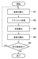
<Fifth embodiment>
A fifth embodiment according to the present invention will be described. In this embodiment, exposure processing performed by the exposure apparatus described in the first to fourth embodiments will be described. FIG. 6 is a flowchart showing the exposure process. Each step of the flowchart shown in FIG. 6 can be controlled by the
S1では、制御部60は、不図示の基板搬送機構を用いて、基板Wを基板ステージ40上に搬入し、基板ステージ40に基板Wを保持させる。S2では、制御部60は、グローバルアライメント処理を行う。例えば、制御部60は、アライメントスコープ(不図示)を用いて、基板Wにおける複数のショット領域のうちサンプルショット領域に形成されたアライメントマークの位置を計測し、その計測結果を統計処理することにより複数のショット領域の配列情報を得る。
In S1, the
S3では、制御部60は、複数のショット領域の各々について走査露光を順次行い、各ショット領域(具体的には、その上の感光材(レジスト))に原版Mのパターンを潜像パターンとして転写する。S3における各ショット領域の走査露光では、上述した第1~第4実施形態で説明したように、計測部50により投影光学系30の光学特性を計測し、その計測結果に基づいて、基板上への露光光ELの照射位置の補正が行われる。即ち、各ショット領域の走査露光において、計測部50での計測結果に基づいた露光光ELの照射位置の補正がリアルタイムで行われうる。
In S3, the
S4では、制御部60は、不図示の基板搬送機構を用いて、基板ステージ40から基板Wを搬出する。S5では、制御部60は、走査露光を行うべき次の基板があるか否かを判断する。次の基板がある場合にはS1に戻り、当該次の基板に対して走査露光を行う。一方、次の基板がない場合には終了する。
In S4, the
<物品の製造方法の実施形態>
本発明の実施形態にかかる物品の製造方法は、例えば、半導体デバイス等のマイクロデバイスや微細構造を有する素子等の物品を製造するのに好適である。本実施形態の物品の製造方法は、基板に塗布された感光剤に上記の露光装置を用いて潜像パターンを形成する工程(基板を露光する工程)と、かかる工程で潜像パターンが形成された基板を現像(加工)する工程とを含む。更に、かかる製造方法は、他の周知の工程(酸化、成膜、蒸着、ドーピング、平坦化、エッチング、レジスト剥離、ダイシング、ボンディング、パッケージング等)を含む。本実施形態の物品の製造方法は、従来の方法に比べて、物品の性能・品質・生産性・生産コストの少なくとも1つにおいて有利である。
<Embodiment of article manufacturing method>
The article manufacturing method according to the embodiment of the present invention is suitable for manufacturing articles such as micro devices such as semiconductor devices and elements having fine structures. The method for manufacturing an article of the present embodiment includes a step of forming a latent image pattern on a photosensitive agent applied to a substrate using the above-mentioned exposure device (a step of exposing the substrate), and a step of forming a latent image pattern in this step. The method includes a step of developing (processing) the substrate. Additionally, such manufacturing methods include other well-known steps (oxidation, deposition, deposition, doping, planarization, etching, resist stripping, dicing, bonding, packaging, etc.). The method for manufacturing an article according to the present embodiment is advantageous in at least one of the performance, quality, productivity, and production cost of the article compared to conventional methods.
発明は上記実施形態に制限されるものではなく、発明の精神及び範囲から離脱することなく、様々な変更及び変形が可能である。従って、発明の範囲を公にするために請求項を添付する。 The invention is not limited to the embodiments described above, and various changes and modifications can be made without departing from the spirit and scope of the invention. Therefore, the following claims are hereby appended to disclose the scope of the invention.
10:照明光学系、20:原版ステージ、30:投影光学系、40:基板ステージ、50:計測部、51:投光部、52:受光部、53:受光面、54:検出部、60:制御部、100:露光装置 10: illumination optical system, 20: original stage, 30: projection optical system, 40: substrate stage, 50: measurement section, 51: light projecting section, 52: light receiving section, 53: light receiving surface, 54: detecting section, 60: Control unit, 100: Exposure device
Claims (19)
複数の光学素子を含み、露光光により原版のパターン像を前記基板に投影する投影光学系と、
前記露光光が経由する前記投影光学系の光学素子を経由して前記投影光学系から射出された計測光を用いて、前記投影光学系の光学特性を計測する計測部と、
前記計測部での計測結果に基づいて、前記基板上での前記露光光の照射位置を補正する制御部と、
を含み、
前記計測部は、前記計測光を受光する受光素子を含み、
前記制御部は、前記受光素子上での前記計測光の位置変動の周波数成分に基づいて、前記複数の光学素子の中から、前記露光光の位置変動に影響を与えている光学素子を特定し、特定した光学素子を駆動することにより前記基板上での前記露光光の照射位置を補正する、ことを特徴とする露光装置。 An exposure device that exposes a substrate,
a projection optical system that includes a plurality of optical elements and projects a pattern image of the original onto the substrate using exposure light;
a measurement unit that measures optical characteristics of the projection optical system using measurement light emitted from the projection optical system via an optical element of the projection optical system through which the exposure light passes;
a control unit that corrects the irradiation position of the exposure light on the substrate based on the measurement result of the measurement unit;
including;
The measurement unit includes a light receiving element that receives the measurement light,
The control unit identifies, from the plurality of optical elements, an optical element that is affecting the positional fluctuation of the exposure light based on a frequency component of the positional fluctuation of the measurement light on the light receiving element. An exposure apparatus , comprising: correcting the irradiation position of the exposure light on the substrate by driving a specified optical element .
露光光により原版のパターン像を前記基板に投影する投影光学系と、a projection optical system that projects a pattern image of the original onto the substrate using exposure light;
前記露光光が経由する前記投影光学系の光学素子を経由して前記投影光学系から射出された計測光を用いて、前記投影光学系の光学特性を計測する計測部と、a measurement unit that measures optical characteristics of the projection optical system using measurement light emitted from the projection optical system via an optical element of the projection optical system through which the exposure light passes;
前記計測部での計測結果に基づいて、前記基板上での前記露光光の照射位置を補正する制御部と、a control unit that corrects the irradiation position of the exposure light on the substrate based on the measurement result of the measurement unit;
を含み、including;
前記計測部は、前記計測光を受光する受光素子を含み、The measurement unit includes a light receiving element that receives the measurement light,
前記制御部は、前記受光素子上での前記計測光の位置変動の周波数成分に基づいて、前記投影光学系内の雰囲気ゆらぎが前記露光光の位置変動に影響を与えていると特定した場合、前記投影光学系内の雰囲気を調整することにより前記基板上での前記露光光の照射位置を補正する、ことを特徴とする露光装置。When the control unit identifies that atmospheric fluctuations within the projection optical system are affecting the positional fluctuations of the exposure light based on the frequency components of the positional fluctuations of the measurement light on the light receiving element, An exposure apparatus characterized in that an irradiation position of the exposure light on the substrate is corrected by adjusting an atmosphere within the projection optical system.
前記受光面は、前記投影光学系の結像位置とは異なる位置に配置されている、ことを特徴とする請求項1乃至3のいずれか1項に記載の露光装置。 The light receiving element has a light receiving surface that receives the measurement light,
4. The exposure apparatus according to claim 1, wherein the light receiving surface is arranged at a position different from an image forming position of the projection optical system.
前記投光部は、前記投影光学系に取り付けられている、ことを特徴とする請求項1乃至4のいずれか1項に記載の露光装置。 The measurement section further includes a light projection section that projects the measurement light into the projection optical system,
5. The exposure apparatus according to claim 1, wherein the light projector is attached to the projection optical system.
前記制御部は、前記検出部での検出結果に更に基づいて、前記投影光学系内での前記露光光の位置変動を推定する、ことを特徴とする請求項10に記載の露光装置。 The measurement unit further includes a detection unit that detects at least one of an incident angle and an incident position of the measurement light into the projection optical system,
11. The exposure apparatus according to claim 10 , wherein the control section estimates a positional variation of the exposure light within the projection optical system based further on the detection result of the detection section.
前記制御部は、前記受光素子上での前記計測光の位置変動と前記第2受光素子上での前記検出光の位置変動との差に基づいて、前記投影光学系内での前記露光光の位置変動を推定する、ことを特徴とする請求項12に記載の露光装置。 The second light receiving element is arranged so that the optical path length of the detection light and the optical path length of the measurement light are the same,
The control unit controls the exposure light within the projection optical system based on the difference between the positional variation of the measurement light on the light receiving element and the positional variation of the detection light on the second light receiving element. 13. The exposure apparatus according to claim 12 , wherein the exposure apparatus estimates positional fluctuations.
前記第2受光素子は、前記第1検出光を受光し、
前記制御部は、前記第2受光素子上での前記第1検出光の位置変動と前記第3受光素子上での前記第2検出光の位置変動との差に基づいて、前記受光素子上での前記計測光の位置変動を補正し、それにより得られた値に基づいて前記投影光学系内での前記露光光の位置変動を推定する、ことを特徴とする請求項12に記載の露光装置。 The detection unit includes a second branching unit that branches the detection light into a first detection light and a second detection light, and a third light receiving element that receives the second detection light without going through the projection optical system. Furthermore, it includes
The second light receiving element receives the first detection light,
The control section is configured to control the position of the first detection light on the second light receiving element based on the difference between the positional variation of the first detection light on the second light receiving element and the positional variation of the second detection light on the third light receiving element. 13. The exposure apparatus according to claim 12 , wherein the exposure apparatus corrects the positional fluctuation of the measurement light and estimates the positional fluctuation of the exposure light within the projection optical system based on the value obtained thereby. .
露光光により原版のパターン像を前記基板に投影する投影光学系と、
前記露光光を射出する露光光源とは異なる光源であり、平行光を射出する計測用光源と、
前記露光光が経由する前記投影光学系の光学素子を経由して、前記計測用光源から射出された計測光を用いて、前記投影光学系の光学特性を計測する計測部と、
前記計測部で計測された結果に基づいて、前記基板上での前記露光光の照射位置の位置変動を推定する制御部と、
を含み、
前記計測部は、前記計測光を受光する受光素子を含み、
前記受光素子は、平行光である前記計測光を受光する、ことを特徴とする露光装置。 An exposure device that exposes a substrate,
a projection optical system that projects a pattern image of the original onto the substrate using exposure light;
a measurement light source that is a light source different from the exposure light source that emits the exposure light and that emits parallel light;
a measurement unit that measures optical characteristics of the projection optical system using measurement light emitted from the measurement light source via an optical element of the projection optical system through which the exposure light passes;
a control unit that estimates a positional change in the irradiation position of the exposure light on the substrate based on the result measured by the measurement unit;
including;
The measurement unit includes a light receiving element that receives the measurement light,
An exposure apparatus characterized in that the light receiving element receives the measurement light that is parallel light .
前記受光面は、前記原版の前記パターン像が前記投影光学系を介して結像する結像位置とは異なる位置に配置されている、ことを特徴とする請求項16に記載の露光装置。17. The exposure apparatus according to claim 16, wherein the light-receiving surface is arranged at a position different from an imaging position at which the pattern image of the original is formed via the projection optical system.
前記工程で露光を行われた前記基板を現像する工程と、を含み、
現像された前記基板から物品を製造することを特徴とする物品の製造方法。 A step of exposing the substrate using the exposure apparatus according to any one of claims 1 to 18 ,
Developing the substrate exposed in the step,
A method for manufacturing an article, comprising manufacturing an article from the developed substrate.
Priority Applications (4)
| Application Number | Priority Date | Filing Date | Title |
|---|---|---|---|
| JP2020004671A JP7453790B2 (en) | 2020-01-15 | 2020-01-15 | Exposure device and article manufacturing method |
| TW109141705A TWI836164B (en) | 2020-01-15 | 2020-11-27 | Exposure devices and methods of manufacturing articles |
| KR1020200181556A KR20210092130A (en) | 2020-01-15 | 2020-12-23 | Exposure apparatus, and method of manufacturing article |
| CN202110037169.4A CN113126448A (en) | 2020-01-15 | 2021-01-12 | Exposure apparatus and method for manufacturing article |
Applications Claiming Priority (1)
| Application Number | Priority Date | Filing Date | Title |
|---|---|---|---|
| JP2020004671A JP7453790B2 (en) | 2020-01-15 | 2020-01-15 | Exposure device and article manufacturing method |
Publications (3)
| Publication Number | Publication Date |
|---|---|
| JP2021110905A JP2021110905A (en) | 2021-08-02 |
| JP2021110905A5 JP2021110905A5 (en) | 2023-01-17 |
| JP7453790B2 true JP7453790B2 (en) | 2024-03-21 |
Family
ID=76772241
Family Applications (1)
| Application Number | Title | Priority Date | Filing Date |
|---|---|---|---|
| JP2020004671A Active JP7453790B2 (en) | 2020-01-15 | 2020-01-15 | Exposure device and article manufacturing method |
Country Status (3)
| Country | Link |
|---|---|
| JP (1) | JP7453790B2 (en) |
| KR (1) | KR20210092130A (en) |
| CN (1) | CN113126448A (en) |
Citations (8)
| Publication number | Priority date | Publication date | Assignee | Title |
|---|---|---|---|---|
| JP2001235308A (en) | 2000-02-22 | 2001-08-31 | Nec Corp | Alignment variation measuring apparatus |
| JP2005294608A (en) | 2004-04-01 | 2005-10-20 | Nikon Corp | Electric discharge light source unit, lighting optical device, aligner, and exposure method |
| US20060146304A1 (en) | 2004-12-13 | 2006-07-06 | Carl Zeiss Smt Ag | Method of manufacturing a miniaturized device |
| JP2006179930A (en) | 2004-12-23 | 2006-07-06 | Asml Netherlands Bv | Lithographic apparatus and method of manufacturing device |
| JP2009105378A (en) | 2007-08-17 | 2009-05-14 | Asml Holding Nv | Real time telecentricity measurement |
| JP2011510494A (en) | 2008-01-16 | 2011-03-31 | カール・ツァイス・エスエムティー・ゲーエムベーハー | Projection exposure apparatus for microlithography with measuring means |
| JP2014135368A (en) | 2013-01-09 | 2014-07-24 | Canon Inc | Exposure device, measurement method and method of manufacturing device |
| JP2017072678A (en) | 2015-10-06 | 2017-04-13 | キヤノン株式会社 | Exposure equipment, exposure method, and manufacturing method of article |
Family Cites Families (3)
| Publication number | Priority date | Publication date | Assignee | Title |
|---|---|---|---|---|
| JP3448614B2 (en) * | 1993-08-12 | 2003-09-22 | 株式会社ニコン | Projection exposure method, scanning projection exposure apparatus, and element manufacturing method |
| JPH10289864A (en) * | 1997-04-11 | 1998-10-27 | Nikon Corp | Projection exposing device |
| JP2017172678A (en) * | 2016-03-23 | 2017-09-28 | Ntn株式会社 | Roller bearing for cryogenic environment |
-
2020
- 2020-01-15 JP JP2020004671A patent/JP7453790B2/en active Active
- 2020-12-23 KR KR1020200181556A patent/KR20210092130A/en active Search and Examination
-
2021
- 2021-01-12 CN CN202110037169.4A patent/CN113126448A/en active Pending
Patent Citations (8)
| Publication number | Priority date | Publication date | Assignee | Title |
|---|---|---|---|---|
| JP2001235308A (en) | 2000-02-22 | 2001-08-31 | Nec Corp | Alignment variation measuring apparatus |
| JP2005294608A (en) | 2004-04-01 | 2005-10-20 | Nikon Corp | Electric discharge light source unit, lighting optical device, aligner, and exposure method |
| US20060146304A1 (en) | 2004-12-13 | 2006-07-06 | Carl Zeiss Smt Ag | Method of manufacturing a miniaturized device |
| JP2006179930A (en) | 2004-12-23 | 2006-07-06 | Asml Netherlands Bv | Lithographic apparatus and method of manufacturing device |
| JP2009105378A (en) | 2007-08-17 | 2009-05-14 | Asml Holding Nv | Real time telecentricity measurement |
| JP2011510494A (en) | 2008-01-16 | 2011-03-31 | カール・ツァイス・エスエムティー・ゲーエムベーハー | Projection exposure apparatus for microlithography with measuring means |
| JP2014135368A (en) | 2013-01-09 | 2014-07-24 | Canon Inc | Exposure device, measurement method and method of manufacturing device |
| JP2017072678A (en) | 2015-10-06 | 2017-04-13 | キヤノン株式会社 | Exposure equipment, exposure method, and manufacturing method of article |
Also Published As
| Publication number | Publication date |
|---|---|
| TW202129431A (en) | 2021-08-01 |
| JP2021110905A (en) | 2021-08-02 |
| KR20210092130A (en) | 2021-07-23 |
| CN113126448A (en) | 2021-07-16 |
Similar Documents
| Publication | Publication Date | Title |
|---|---|---|
| KR101914536B1 (en) | Lithographic apparatus | |
| US7965387B2 (en) | Image plane measurement method, exposure method, device manufacturing method, and exposure apparatus | |
| US6819414B1 (en) | Aberration measuring apparatus, aberration measuring method, projection exposure apparatus having the same measuring apparatus, device manufacturing method using the same measuring method, and exposure method | |
| EP1079223A1 (en) | Aberration measuring instrument and measuring method, projection exposure apparatus provided with the instrument and device-manufacturing method using the measuring method, and exposure method | |
| JP5457767B2 (en) | Exposure apparatus and device manufacturing method | |
| JP2785146B2 (en) | Automatic focus adjustment controller | |
| JP3308063B2 (en) | Projection exposure method and apparatus | |
| TW561245B (en) | Interferometer system | |
| US20100209832A1 (en) | Measurement apparatus, exposure apparatus, and device fabrication method | |
| JP5447388B2 (en) | Autofocus system with error compensation | |
| JP4692862B2 (en) | Inspection apparatus, exposure apparatus provided with the inspection apparatus, and method for manufacturing microdevice | |
| JP5386463B2 (en) | Lithographic apparatus | |
| US6744512B2 (en) | Position measuring apparatus and exposure apparatus | |
| US6400456B1 (en) | Plane positioning apparatus | |
| JP2002170754A (en) | Exposure system, method of detecting optical characteristic, and exposure method | |
| JP5489849B2 (en) | Position measuring apparatus and method, exposure apparatus and device manufacturing method | |
| JP7453790B2 (en) | Exposure device and article manufacturing method | |
| JP4376624B2 (en) | Multipath interferometry | |
| TWI836164B (en) | Exposure devices and methods of manufacturing articles | |
| JPH0786136A (en) | Plane position setter | |
| US20160025480A1 (en) | Interferometric level sensor | |
| JP2005345298A (en) | Position detection device and its method, and exposure device and its method | |
| JPH11325821A (en) | Stage controlling method and aligner | |
| JP2006147989A (en) | Measuring apparatus, and exposure equipment | |
| WO2010143652A1 (en) | Method and apparatus for exposure and device fabricating method |
Legal Events
| Date | Code | Title | Description |
|---|---|---|---|
| RD01 | Notification of change of attorney |
Free format text: JAPANESE INTERMEDIATE CODE: A7421 Effective date: 20210103 |
|
| A521 | Request for written amendment filed |
Free format text: JAPANESE INTERMEDIATE CODE: A523 Effective date: 20210113 |
|
| A521 | Request for written amendment filed |
Free format text: JAPANESE INTERMEDIATE CODE: A523 Effective date: 20221223 |
|
| A621 | Written request for application examination |
Free format text: JAPANESE INTERMEDIATE CODE: A621 Effective date: 20221223 |
|
| A977 | Report on retrieval |
Free format text: JAPANESE INTERMEDIATE CODE: A971007 Effective date: 20231002 |
|
| A131 | Notification of reasons for refusal |
Free format text: JAPANESE INTERMEDIATE CODE: A131 Effective date: 20231010 |
|
| A521 | Request for written amendment filed |
Free format text: JAPANESE INTERMEDIATE CODE: A523 Effective date: 20231129 |
|
| TRDD | Decision of grant or rejection written | ||
| A01 | Written decision to grant a patent or to grant a registration (utility model) |
Free format text: JAPANESE INTERMEDIATE CODE: A01 Effective date: 20240209 |
|
| A61 | First payment of annual fees (during grant procedure) |
Free format text: JAPANESE INTERMEDIATE CODE: A61 Effective date: 20240308 |
|
| R151 | Written notification of patent or utility model registration |
Ref document number: 7453790 Country of ref document: JP Free format text: JAPANESE INTERMEDIATE CODE: R151 |