KR20170007724A - Conductive paste, production method for conductive paste, connection structure, and production method for connection structure - Google Patents
Conductive paste, production method for conductive paste, connection structure, and production method for connection structure Download PDFInfo
- Publication number
- KR20170007724A KR20170007724A KR1020167012326A KR20167012326A KR20170007724A KR 20170007724 A KR20170007724 A KR 20170007724A KR 1020167012326 A KR1020167012326 A KR 1020167012326A KR 20167012326 A KR20167012326 A KR 20167012326A KR 20170007724 A KR20170007724 A KR 20170007724A
- Authority
- KR
- South Korea
- Prior art keywords
- conductive paste
- conductive
- electrode
- thermosetting
- particles
- Prior art date
Links
Images


Classifications
-
- C—CHEMISTRY; METALLURGY
- C09—DYES; PAINTS; POLISHES; NATURAL RESINS; ADHESIVES; COMPOSITIONS NOT OTHERWISE PROVIDED FOR; APPLICATIONS OF MATERIALS NOT OTHERWISE PROVIDED FOR
- C09J—ADHESIVES; NON-MECHANICAL ASPECTS OF ADHESIVE PROCESSES IN GENERAL; ADHESIVE PROCESSES NOT PROVIDED FOR ELSEWHERE; USE OF MATERIALS AS ADHESIVES
- C09J9/00—Adhesives characterised by their physical nature or the effects produced, e.g. glue sticks
- C09J9/02—Electrically-conducting adhesives
-
- C—CHEMISTRY; METALLURGY
- C09—DYES; PAINTS; POLISHES; NATURAL RESINS; ADHESIVES; COMPOSITIONS NOT OTHERWISE PROVIDED FOR; APPLICATIONS OF MATERIALS NOT OTHERWISE PROVIDED FOR
- C09J—ADHESIVES; NON-MECHANICAL ASPECTS OF ADHESIVE PROCESSES IN GENERAL; ADHESIVE PROCESSES NOT PROVIDED FOR ELSEWHERE; USE OF MATERIALS AS ADHESIVES
- C09J11/00—Features of adhesives not provided for in group C09J9/00, e.g. additives
- C09J11/02—Non-macromolecular additives
- C09J11/04—Non-macromolecular additives inorganic
-
- C—CHEMISTRY; METALLURGY
- C09—DYES; PAINTS; POLISHES; NATURAL RESINS; ADHESIVES; COMPOSITIONS NOT OTHERWISE PROVIDED FOR; APPLICATIONS OF MATERIALS NOT OTHERWISE PROVIDED FOR
- C09J—ADHESIVES; NON-MECHANICAL ASPECTS OF ADHESIVE PROCESSES IN GENERAL; ADHESIVE PROCESSES NOT PROVIDED FOR ELSEWHERE; USE OF MATERIALS AS ADHESIVES
- C09J163/00—Adhesives based on epoxy resins; Adhesives based on derivatives of epoxy resins
-
- C—CHEMISTRY; METALLURGY
- C09—DYES; PAINTS; POLISHES; NATURAL RESINS; ADHESIVES; COMPOSITIONS NOT OTHERWISE PROVIDED FOR; APPLICATIONS OF MATERIALS NOT OTHERWISE PROVIDED FOR
- C09J—ADHESIVES; NON-MECHANICAL ASPECTS OF ADHESIVE PROCESSES IN GENERAL; ADHESIVE PROCESSES NOT PROVIDED FOR ELSEWHERE; USE OF MATERIALS AS ADHESIVES
- C09J201/00—Adhesives based on unspecified macromolecular compounds
-
- H—ELECTRICITY
- H01—ELECTRIC ELEMENTS
- H01B—CABLES; CONDUCTORS; INSULATORS; SELECTION OF MATERIALS FOR THEIR CONDUCTIVE, INSULATING OR DIELECTRIC PROPERTIES
- H01B1/00—Conductors or conductive bodies characterised by the conductive materials; Selection of materials as conductors
-
- H—ELECTRICITY
- H01—ELECTRIC ELEMENTS
- H01B—CABLES; CONDUCTORS; INSULATORS; SELECTION OF MATERIALS FOR THEIR CONDUCTIVE, INSULATING OR DIELECTRIC PROPERTIES
- H01B1/00—Conductors or conductive bodies characterised by the conductive materials; Selection of materials as conductors
- H01B1/20—Conductive material dispersed in non-conductive organic material
- H01B1/22—Conductive material dispersed in non-conductive organic material the conductive material comprising metals or alloys
-
- H—ELECTRICITY
- H01—ELECTRIC ELEMENTS
- H01B—CABLES; CONDUCTORS; INSULATORS; SELECTION OF MATERIALS FOR THEIR CONDUCTIVE, INSULATING OR DIELECTRIC PROPERTIES
- H01B13/00—Apparatus or processes specially adapted for manufacturing conductors or cables
-
- H—ELECTRICITY
- H01—ELECTRIC ELEMENTS
- H01B—CABLES; CONDUCTORS; INSULATORS; SELECTION OF MATERIALS FOR THEIR CONDUCTIVE, INSULATING OR DIELECTRIC PROPERTIES
- H01B7/00—Insulated conductors or cables characterised by their form
- H01B7/04—Flexible cables, conductors, or cords, e.g. trailing cables
-
- H—ELECTRICITY
- H01—ELECTRIC ELEMENTS
- H01B—CABLES; CONDUCTORS; INSULATORS; SELECTION OF MATERIALS FOR THEIR CONDUCTIVE, INSULATING OR DIELECTRIC PROPERTIES
- H01B7/00—Insulated conductors or cables characterised by their form
- H01B7/08—Flat or ribbon cables
-
- H—ELECTRICITY
- H01—ELECTRIC ELEMENTS
- H01R—ELECTRICALLY-CONDUCTIVE CONNECTIONS; STRUCTURAL ASSOCIATIONS OF A PLURALITY OF MUTUALLY-INSULATED ELECTRICAL CONNECTING ELEMENTS; COUPLING DEVICES; CURRENT COLLECTORS
- H01R11/00—Individual connecting elements providing two or more spaced connecting locations for conductive members which are, or may be, thereby interconnected, e.g. end pieces for wires or cables supported by the wire or cable and having means for facilitating electrical connection to some other wire, terminal, or conductive member, blocks of binding posts
- H01R11/01—Individual connecting elements providing two or more spaced connecting locations for conductive members which are, or may be, thereby interconnected, e.g. end pieces for wires or cables supported by the wire or cable and having means for facilitating electrical connection to some other wire, terminal, or conductive member, blocks of binding posts characterised by the form or arrangement of the conductive interconnection between the connecting locations
-
- H—ELECTRICITY
- H05—ELECTRIC TECHNIQUES NOT OTHERWISE PROVIDED FOR
- H05K—PRINTED CIRCUITS; CASINGS OR CONSTRUCTIONAL DETAILS OF ELECTRIC APPARATUS; MANUFACTURE OF ASSEMBLAGES OF ELECTRICAL COMPONENTS
- H05K1/00—Printed circuits
- H05K1/02—Details
- H05K1/14—Structural association of two or more printed circuits
-
- H—ELECTRICITY
- H05—ELECTRIC TECHNIQUES NOT OTHERWISE PROVIDED FOR
- H05K—PRINTED CIRCUITS; CASINGS OR CONSTRUCTIONAL DETAILS OF ELECTRIC APPARATUS; MANUFACTURE OF ASSEMBLAGES OF ELECTRICAL COMPONENTS
- H05K3/00—Apparatus or processes for manufacturing printed circuits
- H05K3/22—Secondary treatment of printed circuits
- H05K3/28—Applying non-metallic protective coatings
-
- H—ELECTRICITY
- H05—ELECTRIC TECHNIQUES NOT OTHERWISE PROVIDED FOR
- H05K—PRINTED CIRCUITS; CASINGS OR CONSTRUCTIONAL DETAILS OF ELECTRIC APPARATUS; MANUFACTURE OF ASSEMBLAGES OF ELECTRICAL COMPONENTS
- H05K3/00—Apparatus or processes for manufacturing printed circuits
- H05K3/30—Assembling printed circuits with electric components, e.g. with resistor
- H05K3/32—Assembling printed circuits with electric components, e.g. with resistor electrically connecting electric components or wires to printed circuits
- H05K3/34—Assembling printed circuits with electric components, e.g. with resistor electrically connecting electric components or wires to printed circuits by soldering
-
- H—ELECTRICITY
- H05—ELECTRIC TECHNIQUES NOT OTHERWISE PROVIDED FOR
- H05K—PRINTED CIRCUITS; CASINGS OR CONSTRUCTIONAL DETAILS OF ELECTRIC APPARATUS; MANUFACTURE OF ASSEMBLAGES OF ELECTRICAL COMPONENTS
- H05K3/00—Apparatus or processes for manufacturing printed circuits
- H05K3/36—Assembling printed circuits with other printed circuits
-
- H—ELECTRICITY
- H01—ELECTRIC ELEMENTS
- H01L—SEMICONDUCTOR DEVICES NOT COVERED BY CLASS H10
- H01L2224/00—Indexing scheme for arrangements for connecting or disconnecting semiconductor or solid-state bodies and methods related thereto as covered by H01L24/00
- H01L2224/01—Means for bonding being attached to, or being formed on, the surface to be connected, e.g. chip-to-package, die-attach, "first-level" interconnects; Manufacturing methods related thereto
- H01L2224/10—Bump connectors; Manufacturing methods related thereto
- H01L2224/11—Manufacturing methods
- H01L2224/115—Manufacturing methods by chemical or physical modification of a pre-existing or pre-deposited material
- H01L2224/1152—Self-assembly, e.g. self-agglomeration of the bump material in a fluid
Abstract
도포 시공성을 높일 수 있고, 또한 도전성 입자를 전극 상에 효율적으로 배치할 수 있고, 전극간의 도통 신뢰성을 높일 수 있는 도전 페이스트를 제공한다. 본 발명에 따른 도전 페이스트는, 열경화성 성분 및 복수의 도전성 입자를 포함하며, 상기 열경화성 성분이, 25℃에서 고형인 열경화성 화합물과 열경화제를 함유하고, 도전 페이스트 중에서, 상기 25℃에서 고형인 열경화성 화합물이 입자상으로 분산되어 있다. The present invention provides a conductive paste capable of enhancing application workability and capable of efficiently disposing conductive particles on an electrode and improving reliability of conduction between electrodes. The conductive paste according to the present invention comprises a thermosetting component and a plurality of conductive particles, wherein the thermosetting component contains a thermosetting compound which is solid at 25 占 폚 and a thermosetting agent, and the thermosetting compound Are dispersed in the form of particles.
Description
본 발명은 도전성 입자를 포함하는 도전 페이스트 및 도전 페이스트의 제조 방법에 관한 것이다. 또한, 본 발명은 상기 도전 페이스트를 사용한 접속 구조체 및 접속 구조체의 제조 방법에 관한 것이다.The present invention relates to a conductive paste containing conductive particles and a method for producing the conductive paste. The present invention also relates to a connection structure using the conductive paste and a manufacturing method of the connection structure.
이방성 도전 페이스트 및 이방성 도전 필름 등의 이방성 도전 재료가 널리 알려져 있다. 상기 이방성 도전 재료에서는, 결합제 수지 중에 도전성 입자가 분산되어 있다.Anisotropic conductive paste such as anisotropic conductive paste and anisotropic conductive film are widely known. In the anisotropic conductive material, the conductive particles are dispersed in the binder resin.
상기 이방성 도전 재료는, 각종 접속 구조체를 얻기 위해서, 예를 들어 플렉시블 프린트 기판과 유리 기판의 접속(FOG(Film on Glass)), 반도체 칩과 플렉시블 프린트 기판의 접속(COF(Chip on Film)), 반도체 칩과 유리 기판의 접속(COG(Chip on Glass)), 및 플렉시블 프린트 기판과 유리 에폭시 기판의 접속(FOB(Film on Board)) 등에 사용되고 있다.The anisotropic conductive material can be used for various connection structures, for example, connection (FOG (Film on Glass)) between a flexible printed board and a glass substrate, connection (COF (Chip on Film)) between a semiconductor chip and a flexible printed board, (COG (Chip on Glass)) between a semiconductor chip and a glass substrate, and connection (FOB (Film on Board)) between a flexible printed substrate and a glass epoxy substrate.
상기 이방성 도전 재료에 의해, 예를 들어 플렉시블 프린트 기판의 전극과 유리 에폭시 기판의 전극을 전기적으로 접속할 때에는, 유리 에폭시 기판 상에 도전성 입자를 포함하는 이방성 도전 재료를 배치한다. 이어서, 플렉시블 프린트 기판을 적층하여, 가열 및 가압한다. 이에 의해, 이방성 도전 재료를 경화시켜서, 도전성 입자를 개재시켜 전극간을 전기적으로 접속하여, 접속 구조체를 얻는다.When the electrodes of the flexible printed circuit board and the electrodes of the glass epoxy substrate are electrically connected by the anisotropic conductive material, an anisotropic conductive material containing conductive particles is disposed on the glass epoxy substrate. Subsequently, the flexible printed circuit board is laminated and heated and pressed. Thereby, the anisotropic conductive material is cured, and the electrodes are electrically connected via the conductive particles to obtain a connection structure.
상기 이방성 도전 재료의 일례로서, 하기 특허문헌 1에는, 열경화성 수지를 포함하는 수지층과, 땜납분과, 경화제를 포함하고, 상기 땜납분과 상기 경화제가 상기 수지층 중에 존재하는 접착 테이프가 개시되어 있다. 이 접착 테이프는 필름상이며, 페이스트상이 아니다.As an example of the anisotropic conductive material,
또한, 특허문헌 1에서는, 상기 접착 테이프를 사용한 접착 방법이 개시되어 있다. 구체적으로는, 제1 기판, 접착 테이프, 제2 기판, 접착 테이프 및 제3 기판을 아래에서부터 이 순서로 적층하여, 적층체를 얻는다. 이때, 제1 기판의 표면에 설치된 제1 전극과, 제2 기판의 표면에 설치된 제2 전극을 대향시킨다. 또한, 제2 기판의 표면에 설치된 제2 전극과 제3 기판의 표면에 설치된 제3 전극을 대향시킨다. 그리고, 적층체를 소정의 온도로 가열해서 접착한다. 이에 의해, 접속 구조체를 얻는다.Further,
또한, 하기 특허문헌 2에는, (A) 소수화 처리가 실시되어 있는 평균 입경 3 내지 100㎚의 실리카 필러와, (B) 접착제 성분과, (C) 도전성 입자를 포함하는 이방성 도전 재료가 개시되어 있다. 특허문헌 2에서는, 상기 실리카 필러의 양이, 상기 접착제 성분의 총량에 대해 10 내지 60질량%이다.Further,
하기 특허문헌 3에는, (1) 1 분자 중에 에폭시기를 평균 1.2개 이상 갖는 에폭시 수지, (2) 0℃ 이하의 연화점 온도를 갖고, 1차 입자 직경이 5㎛ 이하인 고무상 중합체 미립자, (3) 열활성의 잠재성 에폭시 경화제 및 (4) 50℃ 이상의 연화점 온도를 갖고, 1차 입자 직경이 2㎛ 이하인 고연화점 중합체 미립자를 포함하는 이방성 도전 재료가 개시되어 있다.(2) rubber-like polymer fine particles having a primary particle diameter of 5 占 퐉 or less and having a softening point temperature of 0 占 폚 or lower; (3) an epoxy resin having an average particle diameter of 5 占 퐉 or less; (4) an anisotropic conductive material containing a high softening point polymer fine particle having a primary particle diameter of 2 탆 or less and a softening point temperature of 50 캜 or higher.
특허문헌 1에 기재된 접착 테이프는, 필름상이며, 페이스트상이 아니다. 이로 인해, 땜납분을 전극(라인) 상에 효율적으로 배치하는 것은 곤란하다. 예를 들어, 특허문헌 1에 기재된 접착 테이프에서는, 땜납분의 일부가, 전극이 형성되어 있지 않은 영역(스페이스)에도 배치되기 쉽다. 전극이 형성되어 있지 않은 영역에 배치된 땜납분은, 전극간의 도통에 기여하지 않는다.The adhesive tape described in
또한, 땜납분을 포함하는 이방성 도전 페이스트에서도, 땜납분이 전극(라인) 상에 효율적으로 배치되어 있지 않은 경우가 있다. 또한, 특허문헌 2에 기재된 바와 같은 이방성 도전 재료에서는, 스크린 인쇄 등에 의해 도포 시공할 때에 도포 시공성이 낮은 경우가 있다.Further, even in an anisotropic conductive paste containing a solder powder, the solder powder may not be efficiently arranged on the electrode (line). In the case of an anisotropic conductive material as described in
또한, 땜납분을 포함하는 이방성 도전 페이스트의 점도를 낮게 하면, 땜납분이 전극(라인) 상으로 이동하기 쉬워진다. 그러나, 이방성 도전 페이스트의 점도를 낮게 하면, 도포 시공 후의 이방성 도전 페이스트층의 두께가 얇아지거나, 또한 이방성 도전 페이스트가 과도하게 유동하여, 의도치 않은 영역에 배치되거나 하기 쉬워진다.Further, if the viscosity of the anisotropic conductive paste containing the solder powder is made low, the solder powder is likely to move on the electrode (line). However, if the viscosity of the anisotropic conductive paste is lowered, the thickness of the anisotropic conductive paste layer after the application becomes too thin, or the anisotropic conductive paste is excessively flowed, and is easily disposed in an unintended region.
또한, 특허문헌 3에서는, 상기 (1) 에폭시 수지로서, (1-1) 0 내지 50℃의 온도 범위에서 액체의 에폭시 수지와, (1-2) 0 내지 50℃의 온도 범위에서 고형의 에폭시 수지의 혼합물을 사용하는 것이 기재되어 있다. 그러나, 특허문헌 3에서는, 예를 들어 실시예에 있어서, 비스페놀 A형 에폭시 수지인 「에피클론 EP-1004」를 1,6-헥산디올디글리시딜에테르로 용해시키고 있는 바와 같이, 이방성 도전 페이스트 중에 있어서, 고형의 에폭시 수지가 용해하고 있는 구체예가 나타나 있는 것에 지나지 않는다. 이와 같이, 단독으로는 25℃에서 고형의 에폭시 수지라도, 이방성 도전 페이스트 중에서는, 에폭시 수지는 고형의 상태로는 한정하지 않고, 에폭시 수지는 용해한 상태에서 사용되는 것이 일반적이다.(1) a liquid epoxy resin in a temperature range of 0 to 50 캜; and (1-2) a solid epoxy resin in a temperature range of 0 to 50 캜. It is described that a mixture of resins is used. However, in
본 발명의 목적은, 도포 시공성을 높일 수 있고, 또한 도전성 입자를 전극 상에 효율적으로 배치할 수 있어, 전극간의 도통 신뢰성을 높일 수 있는 도전 페이스트 및 도전 페이스트의 제조 방법을 제공하는 것이다. 또한, 본 발명은, 상기 도전 페이스트를 사용한 접속 구조체 및 접속 구조체의 제조 방법을 제공하는 것이다.An object of the present invention is to provide a conductive paste and a conductive paste production method capable of enhancing the application workability and efficiently arranging the conductive particles on the electrode and improving the reliability of the conduction between the electrodes. The present invention also provides a connection structure using the conductive paste and a manufacturing method of the connection structure.
본 발명의 넓은 국면에 따르면, 열경화성 성분 및 복수의 도전성 입자를 포함하며, 상기 열경화성 성분이, 25℃에서 고형인 열경화성 화합물과, 열경화제를 함유하고, 도전 페이스트 중에서, 상기 25℃에서 고형인 열경화성 화합물이 입자상으로 분산되어 있는 도전 페이스트가 제공된다.According to a broad aspect of the present invention, there is provided a thermosetting resin composition comprising a thermosetting component and a plurality of conductive particles, wherein the thermosetting component comprises a thermosetting compound which is solid at 25 占 폚 and a thermosetting agent, There is provided a conductive paste in which the compound is dispersed in a particulate form.
본 발명에 따른 도전 페이스트의 어느 특정한 국면에서는, 상기 도전 페이스트는, 25℃에서 액상인 열경화성 화합물을 함유한다.In a specific aspect of the conductive paste according to the present invention, the conductive paste contains a thermosetting compound which is liquid at 25 占 폚.
본 발명에 따른 도전 페이스트의 어느 특정한 국면에서는, 상기 25℃에서 고형인 열경화성 화합물이, 25℃에서 고형인 열경화성 에폭시 화합물이다.In a specific aspect of the conductive paste according to the present invention, the thermosetting compound solid at 25 캜 is a thermosetting epoxy compound solid at 25 캜.
본 발명에 따른 도전 페이스트의 어느 특정한 국면에서는, 상기 25℃에서 고형인 열경화성 화합물이, 25℃에서 고형인 제1 열경화성 화합물과, 상기 제1 열경화성 화합물과는 다른 융점을 갖고 또한 25℃에서 고형인 제2 열경화성 화합물을 포함한다.In one particular aspect of the conductive paste according to the present invention, the thermosetting compound which is solid at 25 占 폚 has a melting point different from that of the first thermosetting compound at 25 占 폚 and a solid And a second thermosetting compound.
상기 도전성 입자가 땜납을 도전성의 외표면에 갖는 것이 바람직하고, 땜납 입자인 것이 보다 바람직하다.It is preferable that the conductive particles have solder on the conductive outer surface, more preferably solder particles.
본 발명에 따른 도전 페이스트의 어느 특정한 국면에서는, 상기 도전성 입자에 있어서의 땜납의 융점-5℃ 및 5rpm에서의 점도의, 상기 도전성 입자에 있어서의 땜납의 융점-5℃ 및 0.5rpm에서의 점도에 대한 비가 1 이상 2 이하이다.In a specific aspect of the conductive paste according to the present invention, the viscosity of the solder in the conductive particle at the melting point of -5 DEG C and at 5 rpm is not more than the viscosity at -5 DEG C and 0.5 rpm of the solder in the conductive particle The ratio is 1 or more and 2 or less.
본 발명에 따른 도전 페이스트의 어느 특정한 국면에서는, 입자상인 상기 열경화성 화합물의 입자 직경이 1㎛ 이상 40㎛ 이하이다.In a specific aspect of the conductive paste according to the present invention, the particulate thermosetting compound has a particle diameter of 1 占 퐉 or more and 40 占 퐉 or less.
본 발명에 따른 도전 페이스트의 어느 특정한 국면에서는, 25℃ 및 5rpm에서의 점도의, 25℃ 및 0.5rpm에서의 점도에 대한 비가 2.5 이상 7 이하이고, 다른 특정한 국면에서는, 25℃ 및 5rpm에서의 점도의, 25℃ 및 0.5rpm에서의 점도에 대한 비가 4 이상 7 이하이다.In a specific aspect of the conductive paste according to the present invention, the ratio of the viscosity at 25 占 폚 and 5 rpm to the viscosity at 25 占 폚 and 0.5 rpm is not less than 2.5 and not more than 7; in other specific aspects, the viscosity at 25 占 폚 and 5 rpm To the viscosity at 25 DEG C and 0.5 rpm is 4 or more and 7 or less.
본 발명에 따른 도전 페이스트의 어느 특정한 국면에서는, 상기 도전 페이스트는 플럭스를 포함한다.In a specific aspect of the conductive paste according to the present invention, the conductive paste includes a flux.
본 발명에 따른 도전 페이스트의 어느 특정한 국면에서는, 상기 도전 페이스트는 필러를 포함하지 않거나, 또는 도전 페이스트 100중량% 중 필러를 1중량% 이하의 양으로 포함한다.In a specific aspect of the conductive paste according to the present invention, the conductive paste does not include a filler, or the conductive paste contains an amount of 1 wt% or less of 100 wt% of the conductive paste.
본 발명의 넓은 국면에 따르면, 상술한 도전 페이스트의 제조 방법이며, 25℃에서 고형인 열경화성 화합물과 열경화제를 함유하는 열경화성 성분 및 복수의 도전성 입자를 혼합해서 혼합물을 얻고, 다음에 상기 혼합물을, 상기 25℃에서 고형인 열경화성 화합물의 융점 이상이면서 상기 열경화성 성분의 경화 온도 미만으로 가열하여, 상기 25℃에서 고형인 열경화성 화합물을 용융시킨 후에 고화시킴으로써, 상기 25℃에서 고형인 열경화성 화합물이 입자상으로 분산되어 있는 도전 페이스트를 얻거나, 또는 25℃에서 고형인 열경화성 화합물을 입자상으로 한 후에, 입자상이고 또한 25℃에서 고형인 열경화성 화합물과 열경화제를 함유하는 열경화성 성분과, 복수의 도전성 입자를 포함하는 혼합물이고, 또한 상기 25℃에서 고형인 열경화성 화합물이 입자상으로 분산되어 있는 도전 페이스트를 얻는, 도전 페이스트의 제조 방법이 제공된다.According to a broad aspect of the present invention, there is provided a method for producing a conductive paste as described above, which comprises mixing a thermosetting component containing a thermosetting compound which is solid at 25 DEG C and a thermosetting agent, and a plurality of conductive particles to obtain a mixture, The thermosetting compound solid at 25 占 폚 is heated to a temperature not lower than the melting point of the thermosetting compound solid at 25 占 폚 and less than the curing temperature of the thermosetting component so that the thermosetting compound solid at 25 占 폚 is melted and then solidified, Or a mixture of a thermosetting component containing a thermosetting compound and a thermosetting compound which is solid at 25 DEG C and is solid at 25 DEG C and a thermosetting component containing a plurality of conductive particles at 25 DEG C, , And the thermosetting compound which is solid at 25 DEG C is a particle The production method of the conductive paste, to obtain a conductive paste that is dispersed is provided.
본 발명의 넓은 국면에서는, 적어도 1개의 제1 전극을 표면에 갖는 제1 접속 대상 부재와, 적어도 1개의 제2 전극을 표면에 갖는 제2 접속 대상 부재와, 상기 제1 접속 대상 부재와 상기 제2 접속 대상 부재를 접속하고 있는 접속부를 구비하며, 상기 접속부가, 상술한 도전 페이스트에 의해 형성되어 있고, 상기 제1 전극과 상기 제2 전극이, 상기 접속부 중의 상기 도전성 입자에 의해 전기적으로 접속되어 있는 접속 구조체가 제공된다.According to a broad aspect of the present invention, there is provided a liquid crystal display device comprising a first connection target member having at least one first electrode on its surface, a second connection target member having at least one second electrode on its surface, The first electrode and the second electrode are electrically connected to each other by the conductive particles in the connection portion, and the connection portion is formed by the conductive paste described above, A connection structure is provided.
본 발명의 넓은 국면에 따르면, 상술한 도전 페이스트를 사용하여, 적어도 1개의 제1 전극을 표면에 갖는 제1 접속 대상 부재의 표면 상에, 상기 도전 페이스트를 배치하는 공정과, 상기 도전 페이스트의 상기 제1 접속 대상 부재측과는 반대인 표면 상에, 적어도 1개의 제2 전극을 표면에 갖는 제2 접속 대상 부재를, 상기 제1 전극과 상기 제2 전극이 대향하도록 배치하는 공정과, 상기 25℃에서 고형인 열경화성 화합물의 융점 이상이면서 상기 열경화성 성분의 경화 온도 이상으로 상기 도전 페이스트를 가열함으로써, 상기 제1 접속 대상 부재와 상기 제2 접속 대상 부재를 접속하고 있는 접속부를 상기 도전 페이스트에 의해 형성하고, 또한 상기 제1 전극과 상기 제2 전극을 상기 접속부 중의 상기 도전성 입자에 의해 전기적으로 접속하는 공정을 구비하는, 접속 구조체의 제조 방법이 제공된다.According to a broad aspect of the present invention, there is provided a method of manufacturing a conductive paste, comprising the steps of: disposing the conductive paste on a surface of a first connection target member having at least one first electrode on a surface thereof using the conductive paste; Arranging a second connection target member having at least one second electrode on a surface on a surface opposite to the first connection target member side such that the first electrode and the second electrode face each other; The connecting portion connecting the first connection target member and the second connection target member is formed by the conductive paste by heating the conductive paste at a temperature equal to or higher than the melting point of the solid thermosetting compound at a temperature higher than the curing temperature of the thermosetting component And electrically connecting the first electrode and the second electrode with the conductive particles in the connection portion, A method of manufacturing a connection structure is provided.
본 발명에 따른 접속 구조체의 제조 방법의 어느 특정한 국면에서는, 상기 제2 접속 대상 부재를 배치하는 공정 및 상기 접속부를 형성하는 공정에 있어서, 가압을 행하지 않고, 상기 도전 페이스트에는 상기 제2 접속 대상 부재의 중량이 가해진다.In a specific aspect of the method for manufacturing a connection structure according to the present invention, in the step of disposing the second connection target member and the step of forming the connection portion, the conductive paste is not subjected to pressing, Is weighted.
상기 제2 접속 대상 부재가, 수지 필름, 플렉시블 프린트 기판, 플렉시블 플랫 케이블 또는 리지드 플렉시블 기판인 것이 바람직하다.It is preferable that the second connection target member is a resin film, a flexible printed circuit board, a flexible flat cable, or a rigid flexible substrate.
본 발명에 따른 도전 페이스트는, 열경화성 성분 및 복수의 도전성 입자를 포함하며, 상기 열경화성 성분이, 25℃에서 고형인 열경화성 화합물과 열경화제를 함유하고, 또한 본 발명에 따른 도전 페이스트 중에서, 상기 25℃에서 고형인 열경화성 화합물이 입자상으로 분산되어 있으므로, 도전 페이스트의 도포 시공성을 높일 수 있다. 또한, 본 발명에 따른 도전 페이스트를 사용해서 전극간을 전기적으로 접속한 경우에, 도전성 입자를 전극 상에 효율적으로 배치할 수 있어, 전극간의 도통 신뢰성을 높일 수 있다.The conductive paste according to the present invention comprises a thermosetting component and a plurality of conductive particles, wherein the thermosetting component contains a thermosetting compound which is solid at 25 占 폚 and a thermosetting agent, The thermosetting compound which is solid in the form of particles is dispersed in the form of particles, so that the coating performance of the conductive paste can be improved. In addition, when the electrodes are electrically connected using the conductive paste according to the present invention, the conductive particles can be efficiently arranged on the electrodes, and the reliability of the conduction between the electrodes can be improved.
도 1은 본 발명의 일 실시 형태에 따른 도전 페이스트를 사용해서 얻어지는 접속 구조체를 모식적으로 도시하는 부분 절결 정면 단면도이다.
도 2의 (a) 내지 (c)는, 본 발명의 일 실시 형태에 따른 도전 페이스트를 사용하여, 접속 구조체를 제조하는 방법의 일례의 각 공정을 설명하기 위한 단면도이다.
도 3은 접속 구조체의 변형예를 나타내는 부분 절결 정면 단면도이다.
도 4는 본 발명의 일 실시 형태에 따른 도전 페이스트에 사용 가능한 도전성 입자를 모식적으로 도시하는 단면도이다.
도 5는 도전성 입자의 변형예를 도시하는 단면도이다.
도 6은 도전성 입자의 다른 변형예를 도시하는 단면도이다.
도 7은 본 발명의 일 실시 형태에 따른 도전 페이스트에 있어서, 입자상으로 분산된 열경화성 화합물을 나타내는 화상이다.BRIEF DESCRIPTION OF DRAWINGS FIG. 1 is a partially cut-away front sectional view schematically showing a connection structure obtained by using a conductive paste according to an embodiment of the present invention; FIG.
2 (a) to 2 (c) are cross-sectional views for explaining respective steps of an example of a method of manufacturing a connection structure using a conductive paste according to an embodiment of the present invention.
3 is a partial cutaway front sectional view showing a modification of the connection structure.
4 is a cross-sectional view schematically showing conductive particles usable in a conductive paste according to an embodiment of the present invention.
5 is a cross-sectional view showing a modified example of the conductive particle.
6 is a cross-sectional view showing another modification of the conductive particle.
Fig. 7 is an image showing a thermosetting compound dispersed in particles in the conductive paste according to one embodiment of the present invention. Fig.
이하, 본 발명의 상세를 설명한다.Hereinafter, the details of the present invention will be described.
본 발명에 따른 도전 페이스트에서는, 열경화성 성분 및 복수의 도전성 입자를 포함한다. 본 발명에 따른 도전 페이스트에서는, 상기 열경화성 성분이, 25℃에서 고형인 열경화성 화합물과 열경화제를 함유한다. 본 발명에 따른 도전 페이스트 중에서, 상기 25℃에서 고형인 열경화성 화합물은 입자상으로 분산되어 있다.The conductive paste according to the present invention includes a thermosetting component and a plurality of conductive particles. In the conductive paste according to the present invention, the thermosetting component contains a thermosetting compound and a thermosetting agent which are solid at 25 占 폚. Among the conductive pastes according to the present invention, the thermosetting compound which is solid at 25 DEG C is dispersed in particulate form.
본 발명에 따른 도전 페이스트에서는, 상기 구성이 채용되어 있으므로, 도포 시공성을 높일 수 있다. 본 발명에 따른 도전 페이스트는, 디스펜서 및 스크린 인쇄 등의 도포 시공 방법에 의해, 양호하게 도포 시공 가능하다. 이방성 도전 페이스트의 점도를 낮게 하면, 도전성 입자가 전극(라인) 상에 이동하기 쉬워진다. 도전 페이스트 중에서, 25℃에서 고형인 열경화성 화합물이 입자상으로 분산되어 있는 것은, 도포 시공성을 높이는 것에 크게 기여한다. 예를 들어, 도전 페이스트의 점도가 적절하게 높아지고, 또한 도전 페이스트의 요변성이 적절하게 발현하여, 도포 시공 후의 도전 페이스트층의 두께가 얇아지기 어렵고, 또한 도전 페이스트가, 과도하게 유동하기 어려워져서, 의도치 않은 영역에 배치되기 어려워진다. 한편으로, 도전 페이스트의 점도를 높게 하기 위해서, 필러를 소정량으로 배합하면, 필러는, 도전성 입자의 전극 상으로의 이동을 방해한다. 이에 비해, 상기 25℃에서 고형인 열경화성 화합물은, 필러와 비교하여, 도전성 입자의 전극 상으로의 이동을 방해하기 어렵다. 특히, 도전성 입자의 전극 상으로의 이동 시에, 열경화성 화합물이 액상이 되면, 액상이 된 열경화성 화합물은, 도전성 입자의 전극 상으로의 이동을 방해하지 않는다.In the conductive paste according to the present invention, since the above-described constitution is employed, the application workability can be improved. The conductive paste according to the present invention can be preferably applied by a coating method such as a dispenser and screen printing. If the viscosity of the anisotropic conductive paste is lowered, the conductive particles tend to move on the electrode (line). In the conductive paste, the fact that the thermosetting compound, which is solid at 25 占 폚, is dispersed in a particulate form contributes greatly to enhance the application workability. For example, the viscosity of the conductive paste is appropriately increased, and the thixotropy of the conductive paste is appropriately developed, so that the thickness of the conductive paste layer after the application is difficult to be thinned and the conductive paste is difficult to flow excessively, It is difficult to be placed in an unintended area. On the other hand, if the filler is mixed in a predetermined amount in order to increase the viscosity of the conductive paste, the filler hinders the movement of the conductive particles onto the electrode. On the other hand, the thermosetting compound which is solid at 25 占 폚 hardly obstructs the movement of the conductive particles onto the electrodes as compared with the filler. Particularly, when the thermosetting compound becomes a liquid phase upon movement of the conductive particles onto the electrode, the thermosetting compound that has become a liquid does not disturb the movement of the conductive particles onto the electrode.
특히, 본 발명에 따른 도전 페이스트에서는, 상기 구성이 채용되어 있으므로, 전극간을 전기적으로 접속한 경우에, 복수의 도전성 입자가 제1 전극과 제2 전극 사이에 모이기 쉬워, 복수의 도전성 입자를 전극(라인) 상에 효율적으로 배치할 수 있다. 또한, 복수의 도전성 입자의 일부가, 전극이 형성되어 있지 않은 영역(스페이스)에 배치되기 어려워, 전극이 형성되어 있지 않은 영역에 배치되는 도전성 입자의 양을 상당히 적게 할 수 있다. 따라서, 제1 전극과 제2 전극 사이의 도통 신뢰성을 높일 수 있다. 게다가, 접속되면 안되는 가로 방향에 인접하는 전극간의 전기적인 접속을 방지할 수 있어, 절연 신뢰성을 높일 수 있다. 이러한 효과가 얻어지는 것은, 상기 25℃에서 고형인 열경화성 화합물은, 필러와 비교하여, 도전성 입자의 전극 상으로의 이동을 방해하기 어렵기 때문이라고 생각된다.Particularly, in the conductive paste according to the present invention, since the above configuration is employed, when the electrodes are electrically connected, a plurality of conductive particles are easily collected between the first electrode and the second electrode, (Lines). In addition, a part of the plurality of conductive particles is hardly arranged in a region where no electrode is formed (space), so that the amount of conductive particles disposed in an area where no electrode is formed can be significantly reduced. Therefore, the conduction reliability between the first electrode and the second electrode can be improved. In addition, it is possible to prevent the electrical connection between the electrodes adjacent to each other in the transverse direction which should not be connected, and the insulation reliability can be improved. This effect is obtained because it is considered that the thermosetting compound which is solid at 25 占 폚 is less likely to interfere with the movement of the conductive particles onto the electrode as compared with the filler.
본 발명에 따른 도전 페이스트에서는, 도포 시공성의 향상 효과와, 도전성 입자의 전극 상으로의 효율적인 이동에 의한 달성되는 전극간의 도통 신뢰성의 향상 효과의 양쪽을 양립시켜 얻을 수 있다. 또한, 본 발명에 따른 도전 페이스트에서는, 도전성 입자가 땜납을 도전성의 외표면에 갖는 경우에, 입자상의 열경화성 화합물의 구성과, 도전 페이스트 중에서 이동하기 쉬운 도전성 입자의 구성이 상승하여, 본 발명의 효과를 보다 한층 효과적으로 발휘시킨다. 또한, 본 발명에 따른 도전 페이스트에서는, 도전성 입자가 땜납 입자인 경우에, 입자상의 열경화성 화합물의 구성과, 도전 페이스트 중에서 특히 이동하기 쉬운 도전성 입자의 구성이 상승(相乘)하여, 본 발명의 효과를 가일층 효과적으로 발휘시킨다.In the conductive paste according to the present invention, both of the effect of improving the coating workability and the effect of improving the conduction reliability between the electrodes achieved by the efficient movement of the conductive particles onto the electrodes can be obtained. Further, in the conductive paste according to the present invention, when the conductive particles have the solder on the conductive outer surface, the constitution of the particulate thermosetting compound and the constitution of the conductive particles easily moveable in the conductive paste increase, And more effectively. Further, in the conductive paste according to the present invention, when the conductive particles are solder particles, the constitution of the particulate thermosetting compound and the constitution of the conductive particles particularly easy to move in the conductive paste are increased, Thereby effectively exerting the effect.
본 발명에 따른 도전 페이스트의 제조 방법은, (1) 25℃에서 고형인 열경화성 화합물과 열경화제를 함유하는 열경화성 성분 및 복수의 도전성 입자를 혼합해서 혼합물을 얻고, 다음에 상기 혼합물을, 상기 25℃에서 고형인 열경화성 화합물의 융점 이상이면서 상기 열경화성 성분의 경화 온도 미만으로 가열하여, 상기 25℃에서 고형인 열경화성 화합물을 용융시킨 후에 고화시킴으로써, 상기 25℃에서 고형인 열경화성 화합물이 입자상으로 분산되어 있는 도전 페이스트를 얻거나, 또는 (2) 25℃에서 고형인 열경화성 화합물을 입자상으로 한 후에, 입자상이고 또한 25℃에서 고형인 열경화성 화합물과 열경화제를 함유하는 열경화성 성분과, 복수의 도전성 입자와의 혼합물이고, 또한 상기 25℃에서 고형인 열경화성 열경화성 에폭시 화합물이 입자상으로 분산되어 있는 도전 페이스트를 얻는다. 이러한 본 발명에 따른 도전 페이스트의 제조 방법에 의해, 본 발명에 따른 도전 페이스트를 용이하게 얻을 수 있다. 상기 (2)의 방법의 경우에, 25℃에서 고형인 열경화성 화합물을 입자상으로 할 때 열경화제가 이미 혼합되어 있어도 되고, 필요에 따라서 배합되는 25℃에서 액상인 열경화성 화합물이 이미 혼합되어 있어도 된다. 25℃에서 고형인 열경화성 화합물을 입자상으로 할 때 도전성 입자는 혼합되어 있지 않은 것이 바람직하다.The method for producing a conductive paste according to the present invention comprises the steps of (1) mixing a thermosetting component containing a thermosetting compound solid at 25 ° C and a thermosetting agent, and a plurality of conductive particles to obtain a mixture, The thermosetting compound having a solid content at 25 DEG C is dispersed in a particulate state by melting the thermosetting compound at 25 DEG C at a temperature not lower than the melting point of the thermosetting compound that is solid at 25 DEG C and less than the curing temperature of the thermosetting component at 25 DEG C, Or (2) a mixture of a thermosetting component containing a thermosetting compound and a thermosetting agent, which is particulate and solid at 25 DEG C, and a plurality of conductive particles, after the thermosetting compound which is solid at 25 DEG C is converted into a particulate form , And the thermosetting thermosetting epoxy compound solid at 25 [deg. To obtain a conductive paste, which is. The conductive paste according to the present invention can be easily obtained by the method for producing a conductive paste according to the present invention. In the case of the method (2), when the thermosetting compound which is solid at 25 占 폚 is made into a particulate form, the thermosetting agent may be already mixed, and if necessary, the thermosetting compound which is liquid at 25 占 폚 may be already mixed. When the thermosetting compound which is solid at 25 占 폚 is a particulate phase, it is preferable that the conductive particles are not mixed.
또한, 상기 도전 페이스트에 포함되는 상기 도전성 입자는, 땜납을 도전성의 외표면에 갖는 것이 바람직하고, 땜납 입자인 것이 보다 바람직하다. 이러한 바람직한 도전성 입자를 사용하면, 도전성 입자를 전극 상에 보다 한층 효율적으로 배치할 수 있다.The conductive particles contained in the conductive paste preferably have solder on the conductive outer surface, and more preferably solder particles. By using such preferable conductive particles, the conductive particles can be arranged on the electrode more efficiently.
본 발명에 따른 도전 페이스트는, 이하의 본 발명에 따른 접속 구조체의 제조 방법에 적절하게 사용할 수 있다.The conductive paste according to the present invention can be suitably used in the method for producing a connection structure according to the present invention as follows.
본 발명에 따른 접속 구조체의 제조 방법에서는, 도전 페이스트와, 제1 접속 대상 부재와, 제2 접속 대상 부재를 사용한다. 본 발명에 따른 접속 구조체의 제조 방법에서 사용되는 도전 재료는, 도전 필름이 아니고, 도전 페이스트이다. 상기 도전 페이스트는, 복수의 도전성 입자와, 열경화성 성분을 포함한다. 상기 제1 접속 대상 부재는, 적어도 1개의 제1 전극을 표면에 갖는다. 상기 제2 접속 대상 부재는, 적어도 1개의 제2 전극을 표면에 갖는다.In the method for manufacturing a connection structure according to the present invention, a conductive paste, a first connection object member, and a second connection object member are used. The conductive material used in the method for manufacturing a connection structure according to the present invention is not a conductive film but a conductive paste. The conductive paste includes a plurality of conductive particles and a thermosetting component. The first connection target member has at least one first electrode on its surface. The second connection target member has at least one second electrode on its surface.
본 발명에 따른 접속 구조체의 제조 방법은, 상기 제1 접속 대상 부재의 표면 상에, 상기 도전 페이스트를 배치하는 공정과, 상기 도전 페이스트의 상기 제1 접속 대상 부재측과는 반대인 표면 상에, 상기 제2 접속 대상 부재를, 상기 제1 전극과 상기 제2 전극이 대향하도록 배치하는 공정과, 상기 25℃에서 고형인 열경화성 화합물의 융점 이상이면서 상기 열경화성 성분의 경화 온도 이상으로 상기 도전 페이스트를 가열함으로써, 상기 제1 접속 대상 부재와 상기 제2 접속 대상 부재를 접속하고 있는 접속부를 상기 도전 페이스트에 의해 형성하고, 또한 상기 제1 전극과 상기 제2 전극을, 상기 접속부 중의 도전성 입자에 의해 전기적으로 접속하는 공정을 구비한다.A method of manufacturing a connection structure according to the present invention includes the steps of disposing the conductive paste on the surface of the first connection target member and forming a conductive paste on the surface of the conductive paste opposite to the first connection object side, Heating the conductive paste at a temperature not lower than the melting point of the thermosetting compound solid at 25 캜 and not lower than a setting temperature of the thermosetting component at 25 캜, The connection portion connecting the first connection target member and the second connection target member is formed by the conductive paste and the first electrode and the second electrode are electrically connected to each other by the conductive particles in the connection portion And a connecting step.
본 발명에 따른 접속 구조체의 제조 방법에서는, 상기 제2 접속 대상 부재를 배치하는 공정 및 상기 접속부를 형성하는 공정에 있어서, 가압을 행하지 않고, 상기 도전 페이스트에는 상기 제2 접속 대상 부재의 중량이 가해지는 것이 바람직하다. 본 발명에 따른 접속 구조체의 제조 방법에서는, 상기 제2 접속 대상 부재를 배치하는 공정 및 상기 접속부를 형성하는 공정에 있어서, 상기 도전 페이스트에는 상기 제2 접속 대상 부재의 중량의 힘을 초과하는 가압 압력은 가해지지 않는 것이 바람직하다.In the method of manufacturing a connection structure according to the present invention, in the step of disposing the second connection target member and the step of forming the connection portion, the weight of the second connection object member is not applied to the conductive paste, . In the method of manufacturing a connection structure according to the present invention, in the step of disposing the second connection target member and the step of forming the connection portion, the conductive paste is subjected to a pressure exceeding the force of the weight of the second connection object member It is preferable not to apply.
본 발명에 따른 접속 구조체의 제조 방법에서는, 상기 구성이 채용되어 있으므로, 복수의 도전성 입자가 제1 전극과 제2 전극 사이에 모이기 쉬워, 복수의 도전성 입자를 전극(라인) 상에 효율적으로 배치할 수 있다. 또한, 복수의 도전성 입자의 일부가, 전극이 형성되어 있지 않은 영역(스페이스)에 배치되기 어려워, 전극이 형성되어 있지 않은 영역에 배치되는 도전성 입자의 양을 상당히 적게 할 수 있다. 따라서, 제1 전극과 제2 전극 사이의 도통 신뢰성을 높일 수 있다. 게다가, 접속되면 안되는 가로 방향에 인접하는 전극간의 전기적인 접속을 방지할 수 있어, 절연 신뢰성을 높일 수 있다.In the method of manufacturing a connection structure according to the present invention, since the above configuration is adopted, a plurality of conductive particles are easily collected between the first electrode and the second electrode, and a plurality of conductive particles are efficiently arranged on the electrode . In addition, a part of the plurality of conductive particles is hardly arranged in a region where no electrode is formed (space), so that the amount of conductive particles disposed in an area where no electrode is formed can be significantly reduced. Therefore, the conduction reliability between the first electrode and the second electrode can be improved. In addition, it is possible to prevent the electrical connection between the electrodes adjacent to each other in the transverse direction which should not be connected, and the insulation reliability can be improved.
이와 같이, 복수의 도전성 입자를 전극 상에 효율적으로 배치하고, 또한 전극이 형성되어 있지 않은 영역에 배치되는 도전성 입자의 양을 상당히 적게 하기 위해서는, 도전 필름이 아닌, 도전 페이스트를 사용할 필요가 있는 것을, 본 발명자들은 알아내었다.As described above, in order to efficiently dispose a plurality of conductive particles on the electrode and considerably reduce the amount of the conductive particles disposed in the region where no electrode is formed, it is necessary to use a conductive paste other than the conductive film , The present inventors have found out.
또한, 상기 제2 접속 대상 부재를 배치하는 공정 및 상기 접속부를 형성하는 공정에 있어서, 가압을 행하지 않고, 상기 도전 페이스트에, 상기 제2 접속 대상 부재의 중량이 가해지면, 접속부가 형성되기 전에 전극이 형성되어 있지 않은 영역(스페이스)에 배치되어 있던 도전성 입자가 제1 전극과 제2 전극 사이에 보다 한층 모이기 쉬워져서, 복수의 도전성 입자를 전극(라인) 상에 효율적으로 배치할 수 있는 것도, 본 발명자들은 알아내었다. 본 발명에서는, 도전 필름이 아닌, 도전 페이스트를 사용한다고 하는 구성과, 가압을 행하지 않고, 상기 도전 페이스트에는 상기 제2 접속 대상 부재의 중량이 가해지도록 한다고 하는 구성을 조합해서 채용하는 것에는, 본 발명의 효과를 보다 한층 높은 레벨로 얻기 때문에 큰 의미가 있다.In the step of disposing the second connection target member and the step of forming the connection portion, if the weight of the second connection target member is applied to the conductive paste without applying pressure, The conductive particles disposed in the region where the conductive particles are not formed are more likely to gather between the first electrode and the second electrode so that the plurality of conductive particles can be efficiently arranged on the electrode (line) The present inventors have found out. The present invention employs a configuration in which a conductive paste is used instead of a conductive film and a configuration in which the weight of the second connection target member is applied to the conductive paste without applying pressure is used in combination. The effect of the invention is achieved at a higher level, which is significant.
또한, WO2008/023452A1에서는, 땜납분을 전극 표면에 흘러가게 해서 효율적으로 이동시키는 관점에서는, 접착 시에 소정의 압력으로 가압하면 되는 것이 기재되어 있고, 가압 압력은, 땜납 영역을 더욱 확실하게 형성하는 관점에서는, 예를 들어 0㎫ 이상, 바람직하게는 1㎫ 이상으로 하는 것이 기재되어 있고, 또한 접착 테이프에 의도적으로 가하는 압력이 0㎫여도, 접착 테이프 상에 배치된 부재의 자중에 의해, 접착 테이프에 소정의 압력이 가해져도 되는 것이 기재되어 있다. WO2008/023452A1에서는, 접착 테이프에 의도적으로 가하는 압력이 0㎫여도 되는 것은 기재되어 있지만, 0㎫를 초과하는 압력을 부여한 경우와 0㎫로 한 경우의 효과의 차이에 대해서는, 전혀 기재되어 있지 않다.In addition, in WO2008 / 023452A1, it is described that, from the viewpoint of efficiently moving the solder powder on the electrode surface, the solder powder is pressed at a predetermined pressure at the time of bonding, and the pressing pressure is higher than that , It is described that the pressure is 0 MPa or more, preferably 1 MPa or more, and even if the pressure to be intentionally applied to the adhesive tape is 0 MPa, by the self weight of the member disposed on the adhesive tape, A predetermined pressure may be applied to the surface of the substrate. In WO2008 / 023452A1, it is described that the pressure to be intentionally applied to the adhesive tape may be 0 MPa. However, there is no description about the difference in the effect when the pressure exceeding 0 MPa is applied and when the pressure is 0 MPa.
또한, 도전 필름이 아닌, 도전 페이스트를 사용하면, 도전 페이스트의 도포량에 따라, 접속부의 두께를 적절히 조정하는 것도 가능하다. 한편으로, 도전 필름에서는, 접속부의 두께를 변경하거나, 조정하거나 하기 위해서는, 다른 두께의 도전 필름을 준비하거나, 소정의 두께의 도전 필름을 준비하거나 해야 한다는 문제가 있다.If the conductive paste is used instead of the conductive film, the thickness of the connection portion can be appropriately adjusted in accordance with the application amount of the conductive paste. On the other hand, in the case of the conductive film, in order to change or adjust the thickness of the connecting portion, there is a problem that a conductive film having a different thickness or a conductive film having a predetermined thickness must be prepared.
본 발명에 따른 접속 구조체의 제조 방법에서는, 상기 도전성 입자가 땜납을 도전성의 외표면에 갖는 도전성 입자이거나, 또는 땜납 입자인 경우에, 상기 접속부를 형성할 때, 땜납의 융점 이상으로 가열하는 것이 바람직하다. 이 경우에는, 용융한 후에 고화한 땜납부에 의해, 상기 제1 전극과 상기 제2 전극이 보다 견고하게 접합된다. 이 결과, 전극간의 도통 신뢰성이 보다 한층 높아진다.In the method of manufacturing a connection structure according to the present invention, when the conductive particles are conductive particles having solder on the conductive outer surface or solder particles, it is preferable to heat the solder particles to the melting point or more of the solder Do. In this case, the first electrode and the second electrode are more firmly bonded to each other by the solder portion solidified after melting. As a result, the conduction reliability between the electrodes is further enhanced.
이하, 도면을 참조하면서, 본 발명의 구체적인 실시 형태 및 실시예를 설명 함으로써, 본 발명을 명백히 한다.Best Mode for Carrying Out the Invention Hereinafter, the present invention will be clarified by explaining specific embodiments and examples of the present invention with reference to the drawings.
우선, 도 1에, 본 발명의 일 실시 형태에 따른 도전 페이스트를 사용해서 얻어지는 접속 구조체를 모식적으로 부분 절결 정면 단면도로 나타낸다.First, Fig. 1 schematically shows a partially cut-away front cross-sectional view of a connection structure obtained by using a conductive paste according to an embodiment of the present invention.
도 1에 도시하는 접속 구조체(1)는, 제1 접속 대상 부재(2)와, 제2 접속 대상 부재(3)와, 제1 접속 대상 부재(2)와 제2 접속 대상 부재(3)를 접속하고 있는 접속부(4)를 구비한다. 접속부(4)는 열경화성 성분과, 복수의 도전성 입자를 포함하는 도전 페이스트에 의해 형성되어 있다. 이 도전 페이스트에서는, 상기 열경화성 성분이, 25℃에서 고형인 열경화성 화합물과 열경화제를 함유하고, 상기 도전 페이스트 중에서, 상기 25℃에서 고형인 열경화성 화합물은 입자상으로 분산되어 있다. 본 실시 형태에서는, 상기 도전성 입자로서, 땜납 입자를 사용하고 있다.The
접속부(4)는 복수의 땜납 입자가 모여 서로 접합한 땜납부(4A)(도전성 입자)와, 열경화성 성분이 열경화된 경화물부(4B)를 갖는다.The connecting
제1 접속 대상 부재(2)는 표면(상면)에 복수의 제1 전극(2a)을 갖는다. 제2 접속 대상 부재(3)는 표면(하면)에 복수의 제2 전극(3a)을 갖는다. 제1 전극(2a)과 제2 전극(3a)이 땜납부(4A)에 의해 전기적으로 접속되어 있다. 따라서, 제1 접속 대상 부재(2)와 제2 접속 대상 부재(3)가 땜납부(4A)에 의해 전기적으로 접속되어 있다. 또한, 접속부(4)에 있어서, 제1 전극(2a)과 제2 전극(3a) 사이에 모인 땜납부(4A)와는 다른 영역(경화물부(4B) 부분)에서는, 땜납은 존재하지 않는다. 땜납부(4A)와는 다른 영역(경화물부(4B) 부분)에서는, 땜납부(4A)와 이격된 땜납은 존재하지 않는다. 또한, 소량이면, 제1 전극(2a)과 제2 전극(3a) 사이에 모인 땜납부(4A)와는 다른 영역(경화물부(4B) 부분)에, 땜납이 존재하고 있어도 된다.The first
도 1에 도시한 바와 같이, 접속 구조체(1)에서는, 복수의 땜납 입자가 용융한 후, 땜납 입자의 용융물이 전극의 표면을 번진 후에 고화하여, 땜납부(4A)가 형성되어 있다. 이로 인해, 땜납부(4A)와 제1 전극(2a), 및 땜납부(4A)와 제2 전극(3a)의 접속 면적이 커진다. 즉, 땜납 입자를 사용함으로써, 도전성의 외표면이 니켈, 금 또는 구리 등의 금속인 도전성 입자를 사용한 경우와 비교하여, 땜납부(4A)와 제1 전극(2a), 및 땜납부(4A)와 제2 전극(3a)의 접촉 면적이 커진다. 이로 인해, 접속 구조체(1)에 있어서의 도통 신뢰성 및 접속 신뢰성이 높아진다. 또한, 도전 페이스트는, 플럭스를 포함하고 있어도 된다. 도전 페이스트에 포함되는 플럭스는, 일반적으로 가열에 의해 점차 실활한다.As shown in Fig. 1, in the
또한, 도 1에 도시하는 접속 구조체(1)에서는, 땜납부(4A) 모두가, 제1, 제2 전극(2a, 3a)간의 대향하고 있는 영역에 위치해 있다. 도 3에 도시하는 변형예의 접속 구조체(1X)는, 접속부(4X)만이, 도 1에 도시하는 접속 구조체(1)와 다르다. 접속부(4X)는, 땜납부(4XA)와 경화물부(4XB)를 갖는다. 접속 구조체(1X)와 같이, 땜납부(4XA)의 대부분이, 제1, 제2 전극(2a, 3a)의 대향하고 있는 영역에 위치해 있고, 땜납부(4XA)의 일부가 제1, 제2 전극(2a, 3a)의 대향하고 있는 영역으로부터 측방으로 비어져 나와 있어도 된다. 제1, 제2 전극(2a, 3a)의 대향하고 있는 영역으로부터 측방으로 비어져 나와 있는 땜납부(4XA)는, 땜납부(4XA)의 일부이며, 땜납부(4XA)로부터 이격된 땜납은 아니다. 또한, 본 실시 형태에서는, 땜납부에서 이격된 땜납의 양을 적게 할 수 있지만, 땜납부에서 이격된 땜납이 경화물부 중에 존재하고 있어도 된다.In the
땜납 입자의 사용량을 적게 하면, 접속 구조체(1)를 얻는 것이 용이해진다. 땜납 입자의 사용량을 많게 하면, 접속 구조체(1X)를 얻는 것이 용이해진다.When the usage amount of the solder particles is reduced, it is easy to obtain the
이어서, 본 발명의 일 실시 형태에 따른 도전 페이스트를 사용하여, 접속 구조체(1)를 제조하는 방법의 일례를 설명한다.Next, an example of a method of manufacturing the
우선, 제1 전극(2a)을 표면(상면)에 갖는 제1 접속 대상 부재(2)를 준비한다. 이어서, 도 2의 (a)에 도시한 바와 같이, 제1 접속 대상 부재(2)의 표면 상에, 열경화 성분(11B)과, 복수의 땜납 입자(11A)를 포함하는 도전 페이스트(11)를 배치한다(제1 공정). 제1 접속 대상 부재(2)의 제1 전극(2a)이 설치된 표면 상에, 도전 페이스트(11)를 배치한다. 도전 페이스트(11)의 배치 후에 땜납 입자(11A)는 제1 전극(2a)(라인) 상과 제1 전극(2a)이 형성되어 있지 않은 영역(스페이스)상의 양쪽에 배치되어 있다.First, a first
도전 페이스트(11)의 배치 방법으로서는, 특별히 한정되지 않지만, 디스펜서에 의한 도포, 스크린 인쇄 및 잉크젯 장치에 의한 토출 등을 들 수 있다. 그 중에서도, 스크린 인쇄가 바람직하다. 본 발명에 따른 도전 페이스트를 사용함으로써 스크린 인쇄에 의한 도포 시공성이 상당히 양호해져서, 스크린 인쇄를 행해도, 도전 페이스트층을 소정의 두께로 형성할 수 있고, 또한 도전 페이스트의 과도한 번짐을 억제하여, 도전 페이스트가 의도치 않은 영역에 배치되기 어려워진다.The method of disposing the
또한, 제2 전극(3a)을 표면(하면)에 갖는 제2 접속 대상 부재(3)를 준비한다. 이어서, 도 2의 (b)에 도시한 바와 같이, 제1 접속 대상 부재(2)의 표면 상의 도전 페이스트(11)에 있어서, 도전 페이스트(11)의 제1 접속 대상 부재(2)측과는 반대측의 표면 상에, 제2 접속 대상 부재(3)를 배치한다(제2 공정). 도전 페이스트(11)의 표면 상에, 제2 전극(3a) 측으로부터, 제2 접속 대상 부재(3)를 배치한다. 이때, 제1 전극(2a)과 제2 전극(3a)을 대향시킨다.Furthermore, a second
이어서, 25℃에서 고형인 열경화성 화합물의 융점 이상 및 열경화성 성분(11B)의 경화 온도 이상으로 도전 페이스트(11)를 가열한다(제3 공정). 즉, 25℃에서 고형인 열경화성 화합물의 융점 및 열경화성 성분(11B)의 경화 온도 내보다 낮은 온도 이상으로, 도전 페이스트(11)를 가열한다. 바람직하게는, 땜납의 융점 이상, 즉 땜납 입자(11A)의 융점 이상으로, 도전 페이스트(11)를 가열한다. 이 가열 시에는, 전극이 형성되어 있지 않은 영역에 존재해 있던 땜납 입자(11A)는, 제1 전극(2a)과 제2 전극(3a) 사이에 모인다(자기 응집 효과). 본 실시 형태에서는, 도전 필름이 아닌, 도전 페이스트를 사용하고 있기 때문에, 땜납 입자(11A)가, 제1 전극(2a)과 제2 전극(3a) 사이에 효과적으로 모인다. 또한, 땜납 입자(11A)는 용융하여, 서로 접합한다. 또한, 열경화성 성분(11B)은 열경화한다. 이 결과, 도 2의 (c)에 도시한 바와 같이, 제1 접속 대상 부재(2)와 제2 접속 대상 부재(3)를 접속하고 있는 접속부(4)를, 도전 페이스트(11)에 의해 형성한다. 도전 페이스트(11)에 의해 접속부(4)가 형성되고, 복수의 땜납 입자(11A)가 접합함으로써 땜납부(4A)가 형성되고, 열경화성 성분(11B)이 열 경화함으로써 경화물부(4B)가 형성된다. 땜납 입자(3)가 빠르게 이동하면, 제1 전극(2a)과 제2 전극(3a) 사이에 위치하지 않은 땜납 입자(3)의 이동이 개시하고 나서, 제1 전극(2a)과 제2 전극(3a) 사이에 땜납 입자(3)의 이동이 완료될 때까지, 온도를 일정하게 유지하지 않아도 된다.Subsequently, the
또한, 제3 공정 전반에, 예비 가열 공정을 마련해도 된다. 이 예비 가열 공정이란, 도전 페이스트(11)에, 제2 접속 대상 부재(3)의 중량이 가해진 상태에서, 땜납의 용융 온도 이상, 실질적으로 열경화성 성분(11B)이 열경화하지 않는 온도에서, 5초에서 60초의 가열을 행하는 공정을 말한다. 이 공정을 마련함으로써, 땜납 입자의 제1 전극과 제2 전극 사이에 모이려고 하는 작용이 더욱 높아짐과 함께, 제1 접속 대상 부재와 제2 접속 대상 부재 사이에 발생할 가능성이 있는 보이드를 억제할 수 있다.In addition, a preliminary heating step may be provided in the entire third step. This preliminary heating step is a step of heating the
본 실시 형태에서는, 상기 제2 공정 및 상기 제3 공정에 있어서, 가압을 행하지 않는다. 본 실시 형태에서는, 도전 페이스트(11)에는, 제2 접속 대상 부재(3)의 중량이 가해진다. 이로 인해, 접속부(4)의 형성 시에, 땜납 입자(11A)가, 제1 전극(2a)과 제2 전극(3a) 사이에 효과적으로 모인다. 또한, 상기 제2 공정 및 상기 제3 공정 중 적어도 한 쪽에 있어서, 가압을 행하면, 땜납 입자가 제1 전극과 제2 전극 사이로 모이려고 하는 작용이 저해된다. 이것은, 본 발명자들에 의해 발견되었다.In the present embodiment, no pressure is applied in the second step and the third step. In the present embodiment, the weight of the second
이와 같이 하여, 도 1에 도시하는 접속 구조체(1)가 얻어진다. 또한, 상기 제2 공정과 상기 제3 공정은 연속해서 행해져도 된다. 또한, 상기 제2 공정을 행한 후에, 얻어지는 제1 접속 대상 부재(2)와 도전 페이스트(11)와 제2 접속 대상 부재(3)의 적층체를, 가열부로 이동시켜서, 상기 제3 공정을 행해도 된다. 상기 가열을 행하기 위해서, 가열 부재 상에 상기 적층체를 배치해도 되고, 가열된 공간 내에 상기 적층체를 배치해도 된다.In this manner, the
상기 제3 공정에서의 가열 온도는, 25℃에서 고형인 열경화성 화합물의 융점 이상 및 열경화성 성분(11B)의 경화 온도 이상인 것이 바람직하고, 땜납의 융점 이상 및 열경화성 성분의 경화 온도 이상인 것이 바람직하다. 상기 가열 온도는, 바람직하게는 130℃ 이상, 보다 바람직하게는 160℃ 이상, 바람직하게는 450℃ 이하, 보다 바람직하게는 250℃ 이하, 더욱 바람직하게는 200℃ 이하이다.The heating temperature in the third step is preferably not less than the melting point of the thermosetting compound solid at 25 DEG C and not more than the curing temperature of the thermosetting component (11B), preferably not less than the melting point of the solder and not more than the curing temperature of the thermosetting component. The heating temperature is preferably 130 占 폚 or higher, more preferably 160 占 폚 or higher, preferably 450 占 폚 or lower, more preferably 250 占 폚 or lower, further preferably 200 占 폚 or lower.
상기 예비 가열 공정의 온도는, 바람직하게는 100℃ 이상, 보다 바람직하게는 120℃ 이상, 더욱 바람직하게는 140℃ 이상, 바람직하게는 160℃ 미만, 보다 바람직하게는 150℃ 이하이다.The temperature of the preliminary heating step is preferably 100 占 폚 or higher, more preferably 120 占 폚 or higher, further preferably 140 占 폚 or higher, preferably 160 占 폚 or lower, more preferably 150 占 폚 or lower.
또한, 상기 제1 접속 대상 부재는, 적어도 1개의 제1 전극을 갖고 있으면 된다. 상기 제1 접속 대상 부재는 복수의 제1 전극을 갖는 것이 바람직하다. 상기 제2 접속 대상 부재는, 적어도 1개의 제2 전극을 갖고 있으면 된다. 상기 제2 접속 대상 부재는 복수의 제2 전극을 갖는 것이 바람직하다. The first connection target member may have at least one first electrode. It is preferable that the first connection target member has a plurality of first electrodes. The second connection target member may have at least one second electrode. The second connection target member preferably has a plurality of second electrodes.
상기 제1, 제2 접속 대상 부재는, 특별히 한정되지 않는다. 상기 제1, 제2 접속 대상 부재로서는, 구체적으로는, 반도체 칩, 콘덴서 및 다이오드 등의 전자 부품, 및 수지 필름, 프린트 기판, 플렉시블 프린트 기판, 플렉시블 플랫 케이블, 리지드 플렉시블 기판, 유리 에폭시 기판 및 유리 기판 등의 회로 기판 등의 전자 부품 등을 들 수 있다. 상기 제1, 제2 접속 대상 부재는, 전자 부품인 것이 바람직하다.The first and second connection target members are not particularly limited. Specific examples of the first and second connection target members include electronic parts such as a semiconductor chip, a capacitor and a diode, and a resin film, a printed board, a flexible printed board, a flexible flat cable, a rigid flexible board, a glass epoxy board and a glass And electronic parts such as circuit boards such as boards. It is preferable that the first and second connection target members are electronic parts.
상기 제1 접속 대상 부재 및 상기 제2 접속 대상 부재 내의 적어도 한 쪽이, 수지 필름, 플렉시블 프린트 기판, 플렉시블 플랫 케이블 또는 리지드 플렉시블 기판인 것이 바람직하다. 상기 제2 접속 대상 부재가, 수지 필름, 플렉시블 프린트 기판, 플렉시블 플랫 케이블 또는 리지드 플렉시블 기판인 것이 바람직하다. 수지 필름, 플렉시블 프린트 기판, 플렉시블 플랫 케이블 및 리지드 플렉시블 기판은, 유연성이 높고, 비교적 경량이라고 하는 성질을 갖는다. 이러한 접속 대상 부재의 접속에 도전 필름을 사용한 경우에는, 도전성 입자가 전극 상에 모이기 어려운 경향이 있다. 이에 비해, 본 발명에 따른 도전 페이스트를 사용하고 있기 때문에, 수지 필름, 플렉시블 프린트 기판, 플렉시블 플랫 케이블 또는 리지드 플렉시블 기판을 사용했다 하더라도, 도전성 입자를 전극 상에 효율적으로 모을 수 있어, 전극간의 도통 신뢰성을 충분히 높일 수 있다. 수지 필름, 플렉시블 프린트 기판, 플렉시블 플랫 케이블 또는 리지드 플렉시블 기판을 사용하는 경우에, 반도체 칩 등의 다른 접속 대상 부재를 사용한 경우와 비교하여, 가압을 행하지 않는 것에 의한 전극간의 도통 신뢰성의 향상 효과가 보다 한층 효과적으로 얻어진다.It is preferable that at least one of the first connection target member and the second connection target member is a resin film, a flexible printed circuit board, a flexible flat cable, or a rigid flexible substrate. It is preferable that the second connection target member is a resin film, a flexible printed circuit board, a flexible flat cable, or a rigid flexible substrate. Resin films, flexible printed boards, flexible flat cables and rigid flexible boards have high flexibility and relatively light weight properties. In the case where a conductive film is used for connection of such members to be connected, the conductive particles tend not to collect on the electrodes. In contrast, since the conductive paste according to the present invention is used, even if a resin film, a flexible printed circuit board, a flexible flat cable, or a rigid flexible substrate is used, the conductive particles can be efficiently collected on the electrode, Can be sufficiently increased. In the case of using a resin film, a flexible printed circuit board, a flexible flat cable, or a rigid flexible substrate, the effect of improving the reliability of the conduction between the electrodes by not applying the pressure is better compared with the case of using other members to be connected such as a semiconductor chip Can be obtained more effectively.
상기 접속 대상 부재에 설치되어 있는 전극으로서는, 금 전극, 니켈 전극, 주석 전극, 알루미늄 전극, 구리 전극, 은 전극, 몰리브덴 전극, SUS 전극 및 텅스텐 전극 등의 금속 전극을 들 수 있다. 상기 접속 대상 부재가 플렉시블 프린트 기판 또는 플렉시블 플랫 케이블인 경우에는, 상기 전극은 금 전극, 니켈 전극, 주석 전극, 은 전극 또는 구리 전극인 것이 바람직하다. 상기 접속 대상 부재가 유리 기판인 경우에는, 상기 전극은 알루미늄 전극, 구리 전극, 몰리브덴 전극, 은 전극 또는 텅스텐 전극인 것이 바람직하다. 또한, 상기 전극이 알루미늄 전극인 경우에는, 알루미늄만으로 형성된 전극이어도 되고, 금속 산화물층의 표면에 알루미늄층이 적층된 전극이어도 된다. 상기 금속 산화물층의 재료로서는, 3가의 금속 원소가 도핑된 산화인듐 및 3가의 금속 원소가 도핑된 산화아연 등을 들 수 있다. 상기 3가의 금속 원소로서는, Sn, Al 및 Ga 등을 들 수 있다.Examples of the electrode provided on the member to be connected include metal electrodes such as a gold electrode, a nickel electrode, a tin electrode, an aluminum electrode, a copper electrode, a silver electrode, a molybdenum electrode, a SUS electrode, and a tungsten electrode. When the connection target member is a flexible printed circuit board or a flexible flat cable, the electrode is preferably a gold electrode, a nickel electrode, a tin electrode, a silver electrode, or a copper electrode. When the connection target member is a glass substrate, it is preferable that the electrode is an aluminum electrode, a copper electrode, a molybdenum electrode, a silver electrode, or a tungsten electrode. When the electrode is an aluminum electrode, it may be an electrode formed only of aluminum, or an electrode in which an aluminum layer is laminated on the surface of the metal oxide layer. Examples of the material of the metal oxide layer include indium oxide doped with a trivalent metal element and zinc oxide doped with a trivalent metal element. Examples of the trivalent metal element include Sn, Al, and Ga.
상기 제1 전극과 상기 제2 전극이 대향하고 있는 위치에 있어서의 상기 접속부의 거리 D1은 바람직하게는 3㎛ 이상, 보다 바람직하게는 10㎛ 이상, 바람직하게는 100㎛ 이하, 보다 바람직하게는 75㎛ 이하이다. 상기 거리 D1이 상기 하한 이상이면, 접속부와 접속 대상 부재의 접속 신뢰성이 보다 한층 높아진다. 상기 거리 D1이 상기 상한 이하이면, 접속부의 형성 시에 도전성 입자가 전극 상에 보다 한층 모이기 쉬워져, 전극간의 도통 신뢰성이 보다 한층 높아진다.The distance D1 of the connection portion at the position where the first electrode and the second electrode face each other is preferably 3 m or more, more preferably 10 m or more, preferably 100 m or less, more preferably 75 Mu m or less. When the distance D1 is equal to or larger than the lower limit, the connection reliability of the connecting portion and the member to be connected is further increased. When the distance D1 is less than the upper limit, the conductive particles are more likely to gather on the electrode at the time of forming the connecting portion, and the reliability of the conduction between the electrodes is further enhanced.
도전 페이스트 중에 있어서, 입자상인 상기 25℃에서 고형인 열경화성 화합물의 입자 직경은, 바람직하게는 0.1㎛ 이상, 보다 바람직하게는 1㎛ 이상, 바람직하게는 40㎛ 이하, 보다 바람직하게는 30㎛ 이하, 더욱 바람직하게는 20㎛ 이하, 특히 바람직하게는 10㎛ 이하이다.The particle diameter of the thermosetting compound which is solid at 25 占 폚 in the conductive paste in the conductive paste is preferably 0.1 占 퐉 or more, more preferably 1 占 퐉 or more, preferably 40 占 퐉 or less, more preferably 30 占 퐉 or less, More preferably 20 mu m or less, particularly preferably 10 mu m or less.
입자상인 상기 25℃에서 고형인 열경화성 화합물의 입자 직경은, 수평균 입자 직경을 나타낸다. 입자상인 상기 25℃에서 고형인 열경화성 화합물의 입자 직경은, 예를 들어 임의의 입자상인 25℃에서 고형인 열경화성 화합물 50개를 전자 현미경 또는 광학 현미경으로 관찰하고, 평균값을 산출함으로써 구해진다.The particle diameter of the thermosetting compound which is solid at 25 占 폚 in the particulate state indicates the number average particle diameter. The particle diameter of the thermosetting compound solid at 25 占 폚, which is a particulate solid at 25 占 폚, can be obtained by, for example, observing 50 thermosetting compounds solid at 25 占 폚, which are arbitrary particles, with an electron microscope or an optical microscope and calculating an average value.
상기 도전 페이스트의 25℃ 및 5rpm에서의 점도 η1은 바람직하게는 10㎩·s 이상, 보다 바람직하게는 50㎩·s 이상, 더욱 바람직하게는 100㎩·s 이상, 바람직하게는 800㎩·s 이하, 보다 바람직하게는 600㎩·s 이하, 더욱 바람직하게는 500㎩·s이하이다. 상기 점도 η1이 상기 하한 이상 및 상기 상한 이하이면, 도전 페이스트의 도포 시공성 및 도전성 입자의 배치 정밀도가 보다 한층 높아진다.The viscosity η1 of the conductive paste at 25 ° C. and 5 rpm is preferably 10 Pas · s or more, more preferably 50 Pas · s or more, further preferably 100 Pas · s or more, preferably 800 Pas · s or less , More preferably not more than 600 Pa 占 퐏, still more preferably not more than 500 Pa 占 퐏. When the viscosity? 1 is not less than the lower limit and not more than the upper limit, the coating workability of the conductive paste and the arrangement accuracy of the conductive particles are further enhanced.
상기 도전 페이스트의 25℃ 및 0.5rpm에서의 점도 η2는 바람직하게는 1㎩·s 이상, 바람직하게는 100㎩·s이하이다. 상기 점도 η2가 상기 하한 이상 및 상기 상한 이하이면, 도전 페이스트의 도포 시공성 및 도전성 입자의 배치 정밀도가 보다 한층 높아진다.The viscosity? 2 at 25 ° C and 0.5 rpm of the conductive paste is preferably 1 Pas · s or more, and preferably 100 Pas · s or less. When the viscosity? 2 is not less than the lower limit and not more than the upper limit, the coating workability of the conductive paste and the arrangement accuracy of the conductive particles are further enhanced.
25℃ 및 5rpm에서의 점도 η1의, 25℃ 및 0.5rpm에서의 점도 η2에 대한 비(η1/η2)는, 바람직하게는 1 이상, 보다 바람직하게는 2.5 이상, 더욱 바람직하게는 4 이상, 바람직하게는 7 이하, 보다 바람직하게는 6 이하, 더욱 바람직하게는 5이하이다. 상기 비(η1/η2)가 상기 하한 이상 및 상기 상한 이하이면, 도전 페이스트의 도포 시공성 및 도전성 입자의 배치 정밀도가 보다 한층 높아져서, 전극간의 도통 신뢰성이 효과적으로 높아진다.The ratio? 1 /? 2 to the viscosity? 2 at 25 占 폚 and 0.5 rpm of the viscosity? 1 at 25 占 폚 and 5 rpm is preferably at least 1, more preferably at least 2.5, still more preferably at least 4, Is preferably 7 or less, more preferably 6 or less, further preferably 5 or less. When the ratio eta / [eta] 2 is not less than the lower limit and not more than the upper limit, the coating workability of the conductive paste and the placement accuracy of the conductive particles are further increased, and the reliability of the conduction between the electrodes is effectively increased.
도전성 입자가 땜납을 도전성의 외표면에 갖는 경우에, 도전성 입자에 있어서의 땜납의 융점을 T℃로 한다. (T-5)℃ 및 5rpm에서의 점도 η1'의, (T-5)℃ 및 0.5rpm에서의 점도 η2'에 대한 비(η1'/η2')는, 바람직하게는 1 이상, 바람직하게는 2 이하이다. 상기 비(η1'/η2')가 상기 하한 이상 및 상기 상한 이하이면, 도전성 입자의 배치 정밀도가 보다 한층 높아져서, 전극간의 도통 신뢰성이 효과적으로 높아진다.When the conductive particles have solder on the conductive outer surface, the melting point of the solder in the conductive particles is set to T 占 폚. The ratio (? 1 '/? 2') of the viscosity? 1 'at (T-5) ° C and 5 rpm to the viscosity? 2' at (T- 2 or less. If the ratio? 1 '/? 2' is not less than the lower limit and not more than the upper limit, the arrangement accuracy of the conductive particles is further increased, and the reliability of the conduction between the electrodes is effectively increased.
상기 점도는, 배합 성분의 종류, 배합 성분의 배합량, 및 특히 상기 25℃에서 고형인 열경화성 화합물의 분산 상태에 적절히 조정 가능하다.The viscosity can be appropriately adjusted to the kind of the blended component, the blending amount of the blended component, and particularly the dispersion state of the thermosetting compound which is solid at 25 占 폚.
상기 점도는, 예를 들어 E형 점도계(도끼산교사 제조) 등을 사용하여, 25℃ 및 5rpm의 조건, 25℃ 및 0.5rpm의 조건, (T-5)℃ 및 5rpm 및 (T-5)℃ 및 0.5rpm의 조건에서 측정 가능하다.The viscosity was measured at 25 DEG C and 5 rpm, at 25 DEG C and 0.5 rpm, at (T-5) DEG C and at 5 rpm and (T-5), using a E-type viscometer Lt; 0 > C and 0.5 rpm.
상기 도전 페이스트는, 열경화성 성분과 복수의 도전성 입자를 포함한다. 상기 열경화성 성분은, 25℃에서 고형인 열경화성 화합물(가열에 의해 경화 가능한 경화성 화합물)과, 열경화제를 포함한다. 상기 도전 페이스트는, 25℃에서 액상인 열경화성 화합물(가열에 의해 경화 가능한 경화성 화합물)을 포함하는 것이 바람직하다. 상기 도전 페이스트는 플럭스를 포함하는 것이 바람직하다. 상기 도전 페이스트는, 필러를 포함하고 있어도 된다.The conductive paste includes a thermosetting component and a plurality of conductive particles. The thermosetting component includes a thermosetting compound (a curing compound that can be cured by heating) solid at 25 占 폚 and a thermosetting agent. It is preferable that the conductive paste includes a thermosetting compound (a curing compound that can be cured by heating) that is liquid at 25 占 폚. The conductive paste preferably includes a flux. The conductive paste may include a filler.
이하, 본 발명의 다른 상세를 설명한다.Hereinafter, other details of the present invention will be described.
(도전성 입자)(Conductive particles)
상기 도전성 입자는, 접속 대상 부재의 전극간을 전기적으로 접속한다. 상기 도전성 입자는, 도전성을 갖는 입자이면 특별히 한정되지 않는다. 상기 도전성 입자는, 도전부를 도전성의 외표면에 갖고 있으면 된다.The conductive particles electrically connect the electrodes of the member to be connected. The conductive particles are not particularly limited as long as they are conductive particles. The conductive particles may have a conductive portion on a conductive outer surface.
상기 도전성 입자로서는, 예를 들어 유기 입자, 금속 입자를 제외한 무기 입자, 유기 무기 하이브리드 입자 혹은 금속 입자 등의 표면을 도전층(금속층)으로 피복한 도전성 입자나, 실질적으로 금속만으로 구성되는 금속 입자 등을 들 수 있다.Examples of the conductive particles include conductive particles obtained by coating the surface of an organic particle, inorganic particles other than metal particles, organic-inorganic hybrid particles or metal particles with a conductive layer (metal layer), metal particles composed substantially only of metal .
상기 도전 페이스트에 포함되는 상기 도전성 입자는, 땜납을 도전성의 외표면에 갖는 것이 바람직하고, 땜납 입자인 것이 보다 바람직하다. 이하, 땜납을 도전성의 외표면에 갖는 도전성 입자에 대해서 설명한다.The conductive particles contained in the conductive paste preferably have solder on the conductive outer surface, and more preferably solder particles. Hereinafter, the conductive particles having solder on the conductive outer surface will be described.
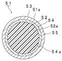
도 4에, 본 발명의 일 실시 형태에 따른 도전 페이스트에 사용 가능한 도전성 입자를 단면도로 나타낸다.Fig. 4 is a cross-sectional view of conductive particles usable in a conductive paste according to an embodiment of the present invention.
도 4에 도시하는 도전성 입자(51)는, 기재 입자(52)(수지 입자 등)와, 기재 입자(52)의 외표면(52a) 상에 배치된 도전부(53)를 갖는다. 도전부(53)는 도전층이다. 도전부(53)는, 기재 입자(52)의 외표면(52a)을 피복하고 있다. 도전성 입자(51)는, 기재 입자(52)의 외표면(52a)이 도전부(53)에 의해 피복된 피복 입자이다. 따라서, 도전성 입자(51)는 도전부(53)를 외표면(51a)에 갖는다.The
도전부(53)는 기재 입자(52)의 외표면(52a) 상에 배치된 제1 도전부(54)(제1 도전층)와, 그 제1 도전부(54)의 외표면(54a) 상에 배치된 땜납부(55)(땜납층, 제2 도전부(제2 도전층))를 갖는다. 도전부(53)의 외측의 표면부(표면층)가, 땜납부(55)이다. 따라서, 도전성 입자(51)는, 도전부(53)의 일부로서 땜납부(55)를 갖고, 또한 기재 입자(52)와 땜납부(55) 사이에, 도전층(53)의 일부로서 땜납부(55)와는 별도로 제1 도전부(54)를 갖는다. 이와 같이, 도전부(53)는, 다층 구조를 갖고 있어도 되고, 2층 이상의 적층 구조를 갖고 있어도 된다.The
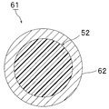
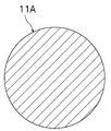
상기한 바와 같이 도전부(53)는 2층 구조를 갖는다. 도 5에 도시하는 변형예와 같이, 도전성 입자(61)는, 단층의 도전부(도전층)로서, 땜납부(62)를 갖고 있어도 된다. 땜납을 도전성의 외표면에 갖는 도전성 입자에서는, 도전성 입자에 있어서의 도전부의 적어도 외측의 표면부(표면층)가, 땜납부이면 된다. 단, 도전성 입자의 제작이 용이하므로, 도전성 입자(51)와 도전성 입자(61) 중, 도전성 입자(51)가 바람직하다. 또한, 도 6에 나타내는 변형예와 같이, 기재 입자를 코어에 갖지 않고, 코어-쉘 입자가 아닌 땜납 입자(11A)를 사용해도 된다. 땜납 입자(11A)는, 중심 부분 및 도전성의 외표면 모두가 땜납에 의해 형성되어 있다.As described above, the
도전성 입자(51, 61) 및 땜납 입자(11A)는, 상기 도전 페이스트에 사용 가능하다. 전극간의 도통 신뢰성을 효과적으로 높이고, 접속 신뢰성도 높이는 관점에서는, 도전성 입자(51, 61) 및 땜납 입자(11A) 중, 땜납 입자(11A)가 특히 바람직하다.The
상기 도전부는 특별히 한정되지 않는다. 상기 도전부를 구성하는 금속으로서는, 금, 은, 구리, 니켈, 팔라듐 및 주석 등을 들 수 있다. 상기 도전층으로서는, 금층, 은층, 구리층, 니켈층, 팔라듐층 또는 주석을 함유하는 도전층 등을 들 수 있다.The conductive portion is not particularly limited. Examples of the metal constituting the conductive portion include gold, silver, copper, nickel, palladium and tin. Examples of the conductive layer include a gold layer, a silver layer, a copper layer, a nickel layer, a palladium layer, or a conductive layer containing tin.
전극과 도전성 입자의 접촉 면적을 크게 하고, 전극간의 도통 신뢰성을 보다 한층 높이는 관점에서는, 상기 도전성 입자는, 수지 입자와, 그 수지 입자의 표면 상에 배치된 도전층(제1 도전층)을 갖는 것이 바람직하다. 전극간의 도통 신뢰성을 보다 한층 높이는 관점에서는, 상기 도전성 입자는, 적어도 도전성의 외측 표면이 저융점 금속층인 도전성 입자인 것이 바람직하다. 상기 도전성 입자는, 기재 입자와, 그 기재 입자의 표면 상에 배치된 도전층을 갖고, 그 도전층의 적어도 외측 표면이, 저융점 금속층인 것이 보다 바람직하다. 상기 도전성 입자는, 기재 입자와, 그 기재 입자의 표면 상에 배치된 도전부를 갖고, 그 도전부의 적어도 외측 표면이, 저융점 금속층인 것이 보다 바람직하다.From the viewpoint of increasing the contact area between the electrode and the conductive particles and further enhancing the reliability of the conduction between the electrodes, the conductive particles have the resin particle and the conductive layer (first conductive layer) disposed on the surface of the resin particle . From the viewpoint of further enhancing the conduction reliability between the electrodes, it is preferable that the above-mentioned conductive particles are conductive particles whose at least conductive outer surface is a low melting point metal layer. It is more preferable that the conductive particles have a base particle and a conductive layer disposed on the surface of the base particle, and at least the outer surface of the conductive layer is a low melting point metal layer. It is more preferable that the conductive particle has base particles and a conductive portion disposed on the surface of the base particle, and at least the outer surface of the conductive portion is a low melting point metal layer.
상기 땜납은, 융점이 450℃ 이하인 저융점 금속인 것이 바람직하다. 상기 땜납 입자는, 융점이 450℃ 이하인 저융점 금속 입자인 것이 바람직하다. 상기 저융점 금속 입자는, 저융점 금속을 포함하는 입자이다. 상기 저융점 금속이란, 융점이 450℃ 이하인 금속을 나타낸다. 저융점 금속의 융점은 바람직하게는 300℃ 이하, 보다 바람직하게는 160℃ 이하이다. 또한, 상기 땜납은 주석을 포함한다. 상기 땜남에 포함되는 금속 100중량% 중, 주석의 함유량은 바람직하게는 30중량% 이상, 보다 바람직하게는 40중량% 이상, 더욱 바람직하게는 70중량% 이상, 특히 바람직하게는 90중량% 이상이다. 상기 땜납에 있어서의 주석의 함유량이 상기 하한 이상이면 땜납부와 전극의 접속 신뢰성이 보다 한층 높아진다.The solder is preferably a low melting point metal having a melting point of 450 캜 or lower. The solder particles are preferably low melting point metal particles having a melting point of 450 캜 or lower. The low melting point metal particles are particles containing a low melting point metal. The low melting point metal means a metal having a melting point of 450 캜 or lower. The melting point of the low melting point metal is preferably 300 DEG C or lower, more preferably 160 DEG C or lower. Further, the solder includes tin. The content of tin is preferably at least 30 wt%, more preferably at least 40 wt%, even more preferably at least 70 wt%, particularly preferably at least 90 wt%, of tin in 100 wt% of the metal contained in the solder . If the content of tin in the solder is lower than the lower limit described above, the connection reliability between the solder portion and the electrode is further enhanced.
또한, 상기 주석의 함유량은, 고주파 유도 결합 플라즈마 발광 분광 분석 장치(호리바세이사꾸쇼사 제조 「ICP-AES」), 또는 형광 X선 분석 장치(시마즈세이사꾸쇼사 제조 「EDX-800HS」) 등을 사용하여 측정 가능하다.The content of the tin may be measured by a high frequency inductively coupled plasma emission spectrochemical analyzer ("ICP-AES" manufactured by Horiba Seisakusho Co., Ltd.) or a fluorescent X-ray analyzer ("EDX-800HS" manufactured by Shimadzu Corporation) . ≪ / RTI >
상기 땜납을 도전성의 외표면에 갖는 도전성 입자를 사용함으로써, 땜납이 용융해서 전극에 접합하여, 땜납부가 전극간을 도통시킨다. 예를 들어, 땜납부와 전극이 점접촉이 아닌 면접촉하기 쉽기 때문에, 접속 저항이 낮아진다. 또한, 땜납을 도전성의 외표면에 갖는 도전성 입자의 사용에 의해, 땜납부와 전극의 접합 강도가 높아지는 결과, 땜납부와 전극의 박리가 보다 한층 발생하기 어려워져서, 도통 신뢰성 및 접속 신뢰성이 효과적으로 높아진다.By using the conductive particles having the solder on the conductive outer surface, the solder is melted and bonded to the electrode, so that the solder portion conducts between the electrodes. For example, since the solder portion and the electrode are likely to come into contact with each other not by point contact, the connection resistance is lowered. In addition, the use of the conductive particles having the solder on the conductive outer surface increases the bonding strength between the solder portion and the electrode, and as a result, the solder portion and the electrode are less likely to be peeled off, effectively increasing the conduction reliability and the connection reliability .
상기 땜납을 구성하는 저융점 금속은 특별히 한정되지 않는다. 상기 저융점 금속은, 주석, 또는 주석을 포함하는 합금인 것이 바람직하다. 상기 합금은, 주석-은 합금, 주석-구리 합금, 주석-은-구리 합금, 주석-비스무트 합금, 주석-아연 합금, 주석-인듐 합금 등을 들 수 있다. 그 중에서도, 전극에 대한 습윤성이 우수한 점에서, 상기 저융점 금속은, 주석, 주석-은 합금, 주석-은-구리 합금, 주석-비스무트 합금, 주석-인듐 합금인 것이 바람직하다. 주석-비스무트 합금, 주석-인듐 합금인 것이 보다 바람직하다.The low melting point metal constituting the solder is not particularly limited. The low melting point metal is preferably an alloy containing tin or tin. The alloy includes tin-silver alloy, tin-copper alloy, tin-silver-copper alloy, tin-bismuth alloy, tin-zinc alloy and tin-indium alloy. Among them, it is preferable that the low melting point metal is tin, a tin-silver alloy, a tin-silver-copper alloy, a tin-bismuth alloy, and a tin-indium alloy from the viewpoint of excellent wettability to electrodes. Tin-bismuth alloy, and tin-indium alloy.
상기 땜납은, JIS Z3001: 용접 용어에 기초하여, 액상선이 450℃ 이하인 용가재인 것이 바람직하다. 상기 땜납의 조성으로서는, 예를 들어 아연, 금, 은, 납, 구리, 주석, 비스무트, 인듐 등을 포함하는 금속 조성을 들 수 있다. 그 중에서도 저융점으로 납 프리인 주석-인듐계(117℃ 공정), 또는 주석-비스무트계(139℃ 공정)이 바람직하다. 즉, 상기 땜납은, 납을 포함하지 않는 것이 바람직하고, 주석과 인듐을 포함하거나, 또는 주석과 비스무트를 포함하는 것이 바람직하다.It is preferable that the solder is a filler material having a liquidus temperature of 450 DEG C or less based on JIS Z3001: welding terminology. Examples of the composition of the solder include a metal composition including zinc, gold, silver, lead, copper, tin, bismuth, indium and the like. Among them, lead-free tin-indium based (117 캜) or tin-bismuth (139 캜) low melting point is preferable. That is, it is preferable that the solder does not contain lead, and includes tin and indium, or includes tin and bismuth.
상기 땜납부와 전극의 접합 강도를 보다 한층 높이기 위해서, 상기 땜납은, 인 및 텔루륨을 포함하고 있어도 되고, 니켈, 구리, 안티몬, 알루미늄, 아연, 철, 금, 티타늄, 게르마늄, 코발트, 비스무트, 망간, 크롬, 몰리브덴, 팔라듐 등의 금속을 포함하고 있어도 된다. 또한, 땜납부와 전극의 접합 강도를 더욱 한층 높이는 관점에서는, 상기 땜납은, 니켈, 구리, 안티몬, 알루미늄 또는 아연을 포함하는 것이 바람직하다. 땜납부와 전극의 접합 강도를 보다 한층 높이는 관점에서는, 접합 강도를 높이기 위한 이들 금속의 함유량은, 땜납 100중량% 중 바람직하게는 0.0001중량% 이상, 바람직하게는 1중량% 이하이다.The solder may include phosphorus and tellurium and may be nickel, copper, antimony, aluminum, zinc, iron, gold, titanium, germanium, cobalt, bismuth, Manganese, chromium, molybdenum, palladium, and the like. From the viewpoint of further enhancing the bonding strength between the solder portion and the electrode, it is preferable that the solder includes nickel, copper, antimony, aluminum or zinc. From the viewpoint of further increasing the bonding strength between the solder portion and the electrode, the content of these metals for increasing the bonding strength is preferably 0.0001 wt% or more, and preferably 1 wt% or less, in 100 wt% of the solder.
상기 도전성 입자의 평균 입자 직경은, 바람직하게는 0.5㎛ 이상, 보다 바람직하게는 1㎛ 이상, 더욱 바람직하게는 3㎛ 이상, 특히 바람직하게는 5㎛ 이상, 바람직하게는 100㎛ 이하, 보다 바람직하게는 30㎛ 이하, 더욱 바람직하게는 20㎛ 이하, 특히 바람직하게는 15㎛ 이하, 가장 바람직하게는 10㎛ 이하이다. 상기 도전성 입자의 평균 입자 직경이 상기 하한 이상 및 상기 상한 이하이면, 도전성 입자를 전극 상에 보다 한층 효율적으로 배치할 수 있다. 상기 도전성 입자의 평균 입자 직경은, 3㎛ 이상 30㎛ 이하인 것이 특히 바람직하다.The average particle diameter of the conductive particles is preferably 0.5 占 퐉 or more, more preferably 1 占 퐉 or more, further preferably 3 占 퐉 or more, particularly preferably 5 占 퐉 or more, preferably 100 占 퐉 or less, Is not more than 30 mu m, more preferably not more than 20 mu m, particularly preferably not more than 15 mu m, and most preferably not more than 10 mu m. When the average particle diameter of the conductive particles is not less than the lower limit and not more than the upper limit, the conductive particles can be more efficiently arranged on the electrode. The average particle diameter of the conductive particles is particularly preferably from 3 탆 to 30 탆.
상기 도전성 입자의 「평균 입자 직경」은, 수평균 입자 직경을 나타낸다. 도전성 입자의 평균 입자 직경은, 예를 들어 임의의 도전성 입자 50개를 전자 현미경 또는 광학 현미경으로 관찰하여, 평균값을 산출함으로써 구해진다.The " average particle diameter " of the conductive particles indicates the number average particle diameter. The average particle diameter of the conductive particles can be obtained, for example, by observing 50 of any conductive particles with an electron microscope or an optical microscope and calculating an average value.
상기 도전 페이스트 100중량% 중, 상기 도전성 입자의 함유량은 바람직하게는 0.1중량% 이상, 보다 바람직하게는 1중량% 이상, 보다 한층 바람직하게는 2중량% 이상, 더욱 바람직하게는 10중량% 이상, 특히 바람직하게는 20중량% 이상, 가장 바람직하게는 30중량% 이상, 바람직하게는 80중량% 이하, 보다 바람직하게는 60중량% 이하, 더욱 바람직하게는 50중량% 이하이다. 상기 도전성 입자의 함유량이 상기 하한 이상 및 상기 상한 이하이면, 전극 상에 도전성 입자를 보다 한층 효율적으로 배치할 수 있고, 전극간에 도전성 입자를 많이 배치하는 것이 용이하여, 도통 신뢰성이 보다 한층 높아진다. 도통 신뢰성을 보다 한층 높이는 관점에서는, 상기 도전성 입자의 함유량은 많은 편이 바람직하다.The content of the conductive particles in 100 wt% of the conductive paste is preferably 0.1 wt% or more, more preferably 1 wt% or more, still more preferably 2 wt% or more, further preferably 10 wt% Particularly preferably not less than 20% by weight, most preferably not less than 30% by weight, preferably not more than 80% by weight, more preferably not more than 60% by weight, further preferably not more than 50% by weight. When the content of the conductive particles is lower than or equal to the lower limit and lower than or equal to the upper limit, the conductive particles can be more efficiently arranged on the electrode, and it is easy to arrange a larger number of conductive particles between the electrodes. From the viewpoint of further enhancing conduction reliability, the content of the conductive particles is preferably large.
(가열에 의해 경화 가능한 화합물: 열경화성 성분)(Compound that can be cured by heating: a thermosetting component)
상기 열경화성 화합물은, 25℃에서 고형이며, 또한 도전 페이스트 중에 입자상으로 분산 가능하면 특별히 한정되지 않는다. 예를 들어, 25℃에 있어서, 상기 도전 페이스트 중에서, 상기 25℃에서 고형인 열경화성 화합물은 입자상으로 분산되어 있다. 또한, 도 7에, 본 발명의 일 실시 형태에 따른 도전 페이스트에 있어서, 입자상으로 분산된 열경화성 화합물의 화상을 나타냈다.The thermosetting compound is not particularly limited as long as it is solid at 25 占 폚 and can be dispersed in the form of particles in the conductive paste. For example, at 25 占 폚, among the conductive paste, the thermosetting compound which is solid at 25 占 폚 is dispersed in particulate form. 7 shows an image of a thermosetting compound dispersed in particles in the conductive paste according to one embodiment of the present invention.
상기 25℃에서 고형인 열경화성 화합물로서는, 옥세탄 화합물, 에폭시 화합물, 에피술피드 화합물, (메트)아크릴 화합물, 페놀화합물, 아미노 화합물, 불포화 폴리에스테르 화합물, 폴리우레탄 화합물, 실리콘 화합물, 폴리이미드 화합물 및 폴리티올 등을 들 수 있다. 상기 25℃에서 고형인 열경화성 화합물은, 1종만이 사용되어도 되고, 2종 이상이 병용되어도 된다.Examples of the thermosetting compound solid at 25 占 폚 include oxetane compounds, epoxy compounds, episulfide compounds, (meth) acrylic compounds, phenol compounds, amino compounds, unsaturated polyester compounds, polyurethane compounds, silicone compounds, polyimide compounds and Polythiol and the like. The thermosetting compound solid at 25 占 폚 may be used alone or in combination of two or more.
도전 페이스트 중에서의 25℃에서 고형인 열경화성 화합물의 분산 상태를 양호하게 하고, 본 발명의 효과를 보다 한층 효과적으로 발휘시키는 관점에서는, 상기 25℃에서 고형인 열경화성 화합물은, 25℃에서 고형인 열경화성 에폭시 화합물인 것이 바람직하다. 또한, 에폭시 화합물의 사용에 의해, 접속 신뢰성이 보다 한층 높아진다.From the viewpoint of improving the dispersion state of the thermosetting compound which is solid at 25 DEG C in the conductive paste and exerting the effect of the present invention more effectively, the thermosetting compound which is solid at 25 DEG C is a thermosetting epoxy compound . Further, by using the epoxy compound, the connection reliability is further enhanced.
전극간의 도통 신뢰성을 효과적으로 높이는 관점에서는, 상기 25℃에서 고형인 열경화성 화합물의 융점은, 바람직하게는 40℃ 이상, 보다 바람직하게는 70℃ 이상, 더욱 바람직하게는 90℃ 이상, 바람직하게는 160℃ 이하, 보다 바람직하게는 140℃ 이하, 더욱 바람직하게는 120℃ 이하이다.From the viewpoint of effectively improving the conduction reliability between the electrodes, the melting point of the thermosetting compound solid at 25 DEG C is preferably 40 DEG C or higher, more preferably 70 DEG C or higher, further preferably 90 DEG C or higher, More preferably not higher than 140 ° C, even more preferably not higher than 120 ° C.
25℃에서 고형인 열경화성 화합물의 용융 시에, 도전 페이스트의 점도를 급격하게 낮추기 어렵게 하여, 도전성 입자의 과도한 침강을 억제하고, 결과적으로 전극간의 도통 신뢰성을 효과적으로 높이는 관점에서는, 상기 25℃에서 고형인 열경화성 화합물이, 25℃에서 고형인 제1 열경화성 화합물과, 상기 제1 열경화성 화합물과는 다른 융점을 갖고 또한 25℃에서 고형인 제2 열경화성 화합물을 포함하는 것이 바람직하다.From the viewpoint of suppressing the viscosity of the conductive paste to a drastic lowering at the time of melting the thermosetting compound solid at 25 占 폚 and suppressing excessive sedimentation of the conductive particles and consequently increasing the reliability of the conduction between the electrodes effectively, It is preferred that the thermosetting compound comprises a first thermosetting compound that is solid at 25 占 폚 and a second thermosetting compound that has a melting point different from that of the first thermosetting compound and is solid at 25 占 폚.
전극간의 도통 신뢰성을 효과적으로 높이는 관점에서는, 상기 제1 열경화성 화합물의 융점과 상기 제2 열경화성 화합물의 융점의 차의 절댓값은 바람직하게는 1℃ 이상, 보다 바람직하게는 5℃ 이상, 더욱 바람직하게는 10℃ 이상, 바람직하게는 30℃ 이하, 보다 바람직하게는 20℃ 이하이다.From the viewpoint of effectively improving the conduction reliability between the electrodes, the absolute value of the difference between the melting point of the first thermosetting compound and the melting point of the second thermosetting compound is preferably 1 DEG C or more, more preferably 5 DEG C or more, still more preferably 10 ° C or higher, preferably 30 ° C or lower, more preferably 20 ° C or lower.
상기 25℃에서 고형인 열경화성 화합물의 분산 상태를 양호하게 하고, 본 발명의 효과를 보다 한층 효과적으로 발휘시키는 관점에서는, 상기 도전 페이스트는, 25℃에서 액상인 열경화성 화합물을 포함하는 것이 바람직하다. 상기 25℃에서 액상인 열경화성 화합물로서는, 옥세탄 화합물, 에폭시 화합물, 에피술피드 화합물, (메트)아크릴 화합물, 페놀화합물, 아미노 화합물, 불포화 폴리에스테르 화합물, 폴리우레탄 화합물, 실리콘 화합물, 폴리이미드 화합물 및 폴리티올 등을 들 수 있다. 상기 25℃에서 액상인 열경화성 화합물은 1종만이 사용되어도 되고, 2종 이상이 병용되어도 된다.From the viewpoint of improving the dispersion state of the thermosetting compound solid at 25 占 폚 and exerting the effect of the present invention more effectively, it is preferable that the conductive paste contains a thermosetting compound which is liquid at 25 占 폚. Examples of the thermosetting compound which is in a liquid phase at 25 占 폚 include oxetane compounds, epoxy compounds, episulfide compounds, (meth) acrylic compounds, phenol compounds, amino compounds, unsaturated polyester compounds, polyurethane compounds, silicone compounds, Polythiol and the like. The above-mentioned thermosetting compound which is liquid at 25 占 폚 may be used alone or two or more of them may be used in combination.
도전 페이스트의 경화성 및 점도를 보다 한층 양호하게 하고, 접속 신뢰성을 보다 한층 높이는 관점에서, 상기 25℃에서 액상인 열경화성 화합물은, 25℃에서 액상인 열경화성 에폭시 화합물인 것이 바람직하다.From the viewpoint of further improving the curability and viscosity of the conductive paste and further improving the connection reliability, it is preferable that the thermosetting compound which is in a liquid phase at 25 캜 is a thermosetting epoxy compound which is liquid at 25 캜.
상기 도전 페이스트 100중량% 중, 상기 25℃에서 고형인 열경화성 화합물과 상기 25℃에서 액상인 열경화성 화합물과의 합계의 함유량은, 바람직하게는 20중량% 이상, 보다 바람직하게는 40중량% 이상, 더욱 바람직하게는 50중량% 이상, 바람직하게는 99중량% 이하, 보다 바람직하게는 98중량% 이하, 더욱 바람직하게는 90중량% 이하, 특히 바람직하게는 80중량% 이하이다. 내충격성을 보다 한층 높이는 관점에서는, 상기 열경화성 성분의 함유량은 많은 편이 바람직하다.The total content of the thermosetting compound solid at 25 占 폚 and the thermosetting compound liquid at 25 占 폚 among 100% by weight of the conductive paste is preferably 20% by weight or more, more preferably 40% by weight or more, Preferably not less than 50% by weight, preferably not more than 99% by weight, more preferably not more than 98% by weight, more preferably not more than 90% by weight, particularly preferably not more than 80% by weight. From the viewpoint of further improving the impact resistance, the content of the above-mentioned thermosetting component is preferably large.
상기 도전 페이스트 100중량% 중, 상기 25℃에서 고형인 열경화성 화합물 및 상기 25℃에서 고형인 열경화성 에폭시 화합물의 함유량은 각각, 바람직하게는 5중량% 이상, 보다 바람직하게는 10중량% 이상, 바람직하게는 70중량% 이하, 보다 바람직하게는 50중량% 이하이다. 상기 25℃에서 고형인 열경화성 화합물 및 상기 25℃에서 고형인 열경화성 에폭시 화합물의 함유량이 상기 하한 이상 및 상기 상한 이하이면, 도전 페이스트의 도포 시공성 및 도전성 입자의 배치 정밀도가 보다 한층 높아진다.The content of the thermosetting compound which is solid at 25 DEG C and the thermosetting epoxy compound which is solid at 25 DEG C in 100 wt% of the conductive paste is preferably 5% by weight or more, more preferably 10% by weight or more, Is not more than 70% by weight, more preferably not more than 50% by weight. If the content of the thermosetting compound which is solid at 25 占 폚 and the thermosetting epoxy compound which is solid at 25 占 폚 is lower than or equal to the lower limit and below the upper limit, the coating workability of the conductive paste and the arrangement accuracy of the conductive particles are further enhanced.
상기 도전 페이스트 100중량% 중, 상기 25℃에서 액상인 열경화성 화합물 및 상기 25℃에서 액상인 열경화성 에폭시 화합물의 함유량은 각각, 바람직하게는 5중량% 이상, 보다 바람직하게는 10중량% 이상, 바람직하게는 70중량% 이하, 보다 바람직하게는 50중량% 이하이다. 상기 25℃에서 액상인 열경화성 화합물 및 상기 25℃에서 액상인 열경화성 에폭시 화합물의 함유량이 상기 하한 이상 및 상기 상한 이하이면, 도전 페이스트의 도포 시공성 및 도전성 입자의 배치 정밀도가 보다 한층 높아진다.The content of the thermosetting compound which is liquid at 25 占 폚 and the thermosetting epoxy compound which is liquid at 25 占 폚 among 100% by weight of the conductive paste is preferably 5% by weight or more, more preferably 10% by weight or more, Is not more than 70% by weight, more preferably not more than 50% by weight. If the content of the thermosetting compound which is liquid at 25 占 폚 and the thermosetting epoxy compound which is liquid at 25 占 폚 is lower than or equal to the lower limit and above the upper limit, the coating workability of the conductive paste and the arrangement accuracy of the conductive particles are further enhanced.
25℃에서 고형인 열경화성 화합물과 25℃에서 액상인 열경화성 화합물의 SP값의 차는, 바람직하게는 0.5 이상, 보다 바람직하게는 1 이상, 바람직하게는 3 이하, 보다 바람직하게는 2 이하이다. SP값의 차가 상기 하한 이상 및 상기 상한 이하이면, 25℃에서 고형인 열경화성 화합물의 입자로서 안정되게 존재할 수 있으며, 또한 도전 페이스트의 도전성 입자의 배치 정밀도가 보다 한층 높아진다.The difference between the SP value of the thermosetting compound which is solid at 25 占 폚 and that of the thermosetting compound which is liquid at 25 占 폚 is preferably 0.5 or more, more preferably 1 or more, preferably 3 or less, more preferably 2 or less. If the difference in SP value is above the lower limit and below the upper limit, it can be stably present as particles of the thermosetting compound which is solid at 25 占 폚, and the positioning accuracy of the conductive particles in the conductive paste is further enhanced.
(열경화제: 열경화성 성분)(Thermosetting agent: thermosetting component)
상기 열경화제는, 상기 열경화성 화합물을 열경화시킨다. 상기 열경화제로서는, 이미다졸 경화제, 아민 경화제, 페놀 경화제, 폴리티올 경화제, 산 무수물, 열 양이온 개시제 및 열 라디칼 발생제 등을 들 수 있다. 상기 열경화제는, 1종만이 사용되어도 되고, 2종 이상이 병용되어도 된다.The thermosetting agent thermally cures the thermosetting compound. Examples of the heat curing agent include an imidazole curing agent, an amine curing agent, a phenol curing agent, a polythiol curing agent, an acid anhydride, a thermal cationic initiator, and a thermal radical generator. The thermosetting agent may be used alone or in combination of two or more.
그 중에서도, 도전 페이스트를 저온에서 보다 한층 빠르게 경화 가능하므로, 이미다졸 경화제, 폴리티올 경화제 또는 아민 경화제가 바람직하다. 또한, 가열에 의해 경화 가능한 경화성 화합물과 상기 열경화제를 혼합했을 때 보존 안정성이 높아지므로, 잠재성의 경화제가 바람직하다. 잠재성의 경화제는, 잠재성 이미다졸 경화제, 잠재성 폴리티올 경화제 또는 잠재성 아민 경화제인 것이 바람직하다. 또한, 상기 열경화제는, 폴리우레탄 수지 또는 폴리에스테르 수지 등의 고분자 물질로 피복되어 있어도 된다.Among them, an imidazole curing agent, a polythiol curing agent or an amine curing agent is preferable because the conductive paste can be cured more rapidly at a low temperature. In addition, when the heat curing agent is mixed with the curing compound that can be cured by heating, the storage stability becomes high, and therefore, a latent curing agent is preferable. The latent curing agent is preferably a latent imidazole curing agent, a latent polythiol curing agent or a latent amine curing agent. The thermosetting agent may be coated with a polymer material such as a polyurethane resin or a polyester resin.
상기 이미다졸 경화제로서는, 특별히 한정되지 않고, 2-메틸이미다졸, 2-에틸-4-메틸이미다졸, 1-시아노에틸-2-페닐이미다졸, 1-시아노에틸-2-페닐이미다졸륨 트리멜리테이트, 2,4-디아미노-6-[2'-메틸이미다졸릴-(1')]-에틸-s-트리아진 및 2,4-디아미노-6-[2'-메틸이미다졸릴-(1')]-에틸-s-트리아진이소시아누르산 부가물 등을 들 수 있다.The imidazole curing agent is not particularly limited, and examples thereof include 2-methylimidazole, 2-ethyl-4-methylimidazole, 1-cyanoethyl- Phenylimidazolium trimellitate, 2,4-diamino-6- [2'-methylimidazolyl- (1 ')] - ethyl-s-triazine and 2,4- diamino-6- [2 '-Methylimidazolyl- (1')] - ethyl-s-triazine isocyanuric acid adduct.
상기 폴리티올 경화제로서는, 특별히 한정되지 않고 트리메틸올프로판트리스-3-머캅토프로피오네이트, 펜타에리트리톨테트라키스-3-머캅토프로피오네이트 및 디펜타에리트리톨헥사-3-머캅토프로피오네이트 등을 들 수 있다.The polythiol curing agent is not particularly limited and includes trimethylolpropane tris-3-mercaptopropionate, pentaerythritol tetrakis-3-mercaptopropionate, and dipentaerythritol hexa-3-mercaptopropionate And the like.
상기 아민 경화제로서는, 특별히 한정되지 않고 헥사메틸렌디아민, 옥타메틸렌디아민, 데카메틸렌디아민, 3,9-비스(3-아미노프로필)-2,4,8,10-테트라스피로[5.5]운데칸, 비스(4-아미노시클로헥실)메탄, 메타페닐렌디아민 및 디아미노디페닐술폰 등을 들 수 있다.The amine curing agent is not particularly limited and includes hexamethylenediamine, octamethylenediamine, decamethylenediamine, 3,9-bis (3-aminopropyl) -2,4,8,10-tetaspiro [5.5] undecane, bis (4-aminocyclohexyl) methane, metaphenylenediamine, and diaminodiphenylsulfone.
상기 열 양이온 경화제로서는, 요오도늄계 양이온 경화제, 옥소늄계 양이온 경화제 및 술포늄계 양이온 경화제 등을 들 수 있다. 상기 요오도늄계 양이온 경화제로서는, 비스(4-tert-부틸페닐)요오도늄헥사플루오로포스페이트 등을 들 수 있다. 상기 옥소늄계 양이온 경화제로서는, 트리메틸옥소늄테트라플루오로보레이트 등을 들 수 있다. 상기 술포늄계 양이온 경화제로서는, 트리-p-톨릴술포늄헥사플루오로포스페이트 등을 들 수 있다.Examples of the thermal cationic curing agent include an iodonium-based cationic curing agent, an oxonium-based cationic curing agent, and a sulfonium-based cationic curing agent. Examples of the iodonium-based cationic curing agent include bis (4-tert-butylphenyl) iodonium hexafluorophosphate and the like. Examples of the oxonium-based cation curing agent include trimethyloxonium tetrafluoroborate and the like. Examples of the sulfonium cation-based curing agent include tri-p-tolylsulfonium hexafluorophosphate and the like.
상기 열 라디칼 발생제로서는, 특별히 한정되지 않고, 아조 화합물 및 유기 과산화물 등을 들 수 있다. 상기 아조 화합물로서는, 아조비스이소부티로니트릴(AIBN) 등을 들 수 있다. 상기 유기 과산화물로서는, 디-tert-부틸퍼옥시드 및 메틸에틸케톤퍼옥시드 등을 들 수 있다.The heat radical generator is not particularly limited, and examples thereof include an azo compound and an organic peroxide. Examples of the azo compound include azobisisobutyronitrile (AIBN) and the like. Examples of the organic peroxide include di-tert-butyl peroxide and methyl ethyl ketone peroxide.
상기 열경화제의 반응 개시 온도(경화 온도)는, 바람직하게는 50℃ 이상, 보다 바람직하게는 70℃ 이상, 더욱 바람직하게는 80℃ 이상, 바람직하게는 250℃ 이하, 보다 바람직하게는 200℃ 이하, 더욱 바람직하게는 150℃ 이하, 특히 바람직하게는 140℃ 이하이다. 상기 열경화제의 반응 개시 온도가 상기 하한 이상 및 상기 상한 이하이면, 도전성 입자가 전극 상에 보다 한층 효율적으로 배치된다. 상기 열경화제의 반응 개시 온도는 80℃ 이상 140℃ 이하인 것이 특히 바람직하다.The reaction initiation temperature (curing temperature) of the heat curing agent is preferably 50 ° C or higher, more preferably 70 ° C or higher, further preferably 80 ° C or higher, preferably 250 ° C or lower, more preferably 200 ° C or lower More preferably 150 ° C or lower, particularly preferably 140 ° C or lower. When the reaction initiation temperature of the heat curing agent is not less than the lower limit and not more than the upper limit, the conductive particles are more efficiently arranged on the electrode. The reaction initiation temperature of the thermosetting agent is particularly preferably from 80 캜 to 140 캜.
도전성 입자를 전극 상에 보다 한층 효율적으로 배치하는 관점에서는, 상기 열경화제의 반응 개시 온도는, 도전성 입자에 있어서의 땜납의 융점보다, 낮은 것이 바람직하고, 5℃ 이상 낮은 것이 보다 바람직하고, 10℃ 이상 낮은 것이 더욱 바람직한다.From the viewpoint of more efficiently arranging the conductive particles on the electrode, the reaction initiation temperature of the heat curing agent is preferably lower than the melting point of the solder in the conductive particle, more preferably 5 deg. C or lower, Or more.
상기 열경화제의 반응 개시 온도는, DSC에서의 발열 피크의 상승 개시의 온도를 의미한다.The reaction initiation temperature of the heat curing agent means the temperature at which the exothermic peak in DSC starts rising.
상기 열경화제의 함유량은 특별히 한정되지 않는다. 상기 25℃에서 고형인 열경화성 화합물 100중량부에 대하여, 상기 열경화제의 함유량은, 바람직하게는 0.01중량부 이상, 보다 바람직하게는 1중량부 이상, 바람직하게는 200 중량부 이하, 보다 바람직하게는 100중량부 이하, 보다 한층 바람직하게는 75 중량부 이하, 더욱 바람직하게는 50 중량부 이하, 특히 바람직하게는 37.5 중량부 이하이다. 상기 25℃에서 고형인 열경화성 화합물과 상기 25℃에서 액상인 열경화성 화합물의 합계 100중량부에 대하여, 상기 열경화제의 함유량은, 바람직하게는 0.01중량부 이상, 보다 바람직하게는 1중량부 이상, 바람직하게는 200 중량부 이하, 보다 바람직하게는 100 중량부 이하, 더욱 바람직하게는 75 중량부 이하이다. 열경화제의 함유량이 상기 하한 이상이면 도전 페이스트를 충분히 경화시키는 것이 용이하다. 열경화제의 함유량이 상기 상한 이하이면, 경화 후에 경화에 관여하지 않은 잉여의 열경화제가 잔존하기 어려워지고, 또한 경화물의 내열성이 보다 한층 높아진다.The content of the thermosetting agent is not particularly limited. The content of the thermosetting agent is preferably at least 0.01 part by weight, more preferably at least 1 part by weight, preferably at most 200 parts by weight, more preferably at most 200 parts by weight, per 100 parts by weight of the thermosetting compound solid at 25 캜 More preferably 100 parts by weight or less, still more preferably 75 parts by weight or less, further preferably 50 parts by weight or less, particularly preferably 37.5 parts by weight or less. The content of the thermosetting agent is preferably 0.01 parts by weight or more, more preferably 1 part by weight or more, and even more preferably 1 part by weight or more per 100 parts by weight of the total of 100 parts by weight of the thermosetting compound solid at 25 캜 and the thermosetting compound liquid at 25 캜 Is not more than 200 parts by weight, more preferably not more than 100 parts by weight, further preferably not more than 75 parts by weight. If the content of the heat curing agent is lower than the lower limit described above, it is easy to sufficiently cure the conductive paste. If the content of the thermosetting agent is less than the upper limit, an excess of the thermosetting agent that is not involved in curing after curing is hard to remain, and the heat resistance of the cured product is further increased.
(플럭스)(Flux)
상기 도전 페이스트는, 플럭스를 포함하는 것이 바람직하다. 상기 도전성 입자가 땜납을 도전성의 표면에 갖는 도전성 입자인 경우에, 플럭스를 사용하는 것이 바람직하다. 플럭스의 사용에 의해, 땜납을 전극 상에 보다 한층 효과적으로 배치할 수 있다. 상기 플럭스는 특별히 한정되지 않는다. 플럭스로서, 땜납 접합 등에 일반적으로 사용되고 있는 플럭스를 사용할 수 있다. 상기 플럭스로서는, 예를 들어 염화아연, 염화아연과 무기 할로겐화물의 혼합물, 염화아연과 무기산의 혼합물, 용융염, 인산, 인산의 유도체, 유기 할로겐화물, 히드라진, 유기산 및 송지 등을 들 수 있다. 상기 플럭스는 1종만이 사용되어도 되고, 2종 이상이 병용되어도 된다.It is preferable that the conductive paste includes a flux. When the conductive particles are conductive particles having solder on the conductive surface, it is preferable to use a flux. By using the flux, the solder can be arranged more effectively on the electrode. The flux is not particularly limited. As the flux, a flux generally used for solder bonding or the like can be used. Examples of the flux include zinc chloride, a mixture of zinc chloride and an inorganic halide, a mixture of zinc chloride and an inorganic acid, a molten salt, a phosphoric acid, a derivative of phosphoric acid, an organic halide, a hydrazine, an organic acid, The flux may be used alone, or two or more fluxes may be used in combination.
상기 용융염으로서는, 염화암모늄 등을 들 수 있다. 상기 유기산으로서는, 락트산, 시트르산, 스테아르산, 글루탐산 및 글루타르산 등을 들 수 있다. 상기 송지로서는, 활성화 송지 및 비활성화 송지 등을 들 수 있다. 상기 플럭스는, 카르복실기를 2개 이상 갖는 유기산, 송지인 것이 바람직하다. 상기 플럭스는, 카르복실기를 2개 이상 갖는 유기산이어도 되고, 송지여도 된다. 카르복실기를 2개 이상 갖는 유기산, 송지의 사용에 의해, 전극간의 도통 신뢰성이 보다 한층 높아진다.Examples of the molten salt include ammonium chloride and the like. Examples of the organic acid include lactic acid, citric acid, stearic acid, glutamic acid and glutaric acid. Examples of the papermaking papers include activated papermaking and inactive papermaking. It is preferable that the flux is an organic acid having two or more carboxyl groups, and a feedstock. The flux may be an organic acid having two or more carboxyl groups, or may be fed. The use of an organic acid having two or more carboxyl groups and a transfer paper makes the reliability of conduction between the electrodes higher.
상기 송지는 아비에트산을 주성분으로 하는 로진류이다. 플럭스는, 로진류인 것이 바람직하고, 아비에트산인 것이 보다 바람직하다. 이 바람직한 플럭스의 사용에 의해, 전극간의 도통 신뢰성이 보다 한층 높아진다.The above paper is a rosin mainly containing abietic acid. The flux is preferably rosin, more preferably abietic acid. By using this preferable flux, the reliability of conduction between the electrodes is further enhanced.
상기 플럭스의 융점은, 바람직하게는 50℃ 이상, 보다 바람직하게는 70℃ 이상, 더욱 바람직하게는 80℃ 이상, 바람직하게는 200℃ 이하, 보다 바람직하게는 160℃ 이하, 보다 한층 바람직하게는 150℃ 이하, 더욱 바람직하게는 140℃ 이하이다. 상기 플럭스의 융점이 상기 하한 이상 및 상기 상한 이하이면, 플럭스 효과가 보다 한층 효과적으로 발휘되고, 땜납 입자가 전극 상에 보다 한층 효율적으로 배치된다. 상기 플럭스의 융점은 80℃ 이상 190℃ 이하인 것이 바람직하다. 상기 플럭스의 융점은 80℃ 이상 140℃ 이하인 것이 특히 바람직하다.The melting point of the flux is preferably 50 占 폚 or higher, more preferably 70 占 폚 or higher, even more preferably 80 占 폚 or higher, preferably 200 占 폚 or lower, more preferably 160 占 폚 or lower, still more preferably 150 Lt; 0 > C, more preferably 140 < 0 > C or less. When the melting point of the flux is higher than or equal to the lower limit and lower than or equal to the upper limit, the flux effect is more effectively exerted and the solder particles are more efficiently arranged on the electrode. The melting point of the flux is preferably 80 ° C or higher and 190 ° C or lower. The melting point of the flux is particularly preferably from 80 캜 to 140 캜.
융점이 80℃ 이상 190℃ 이하인 상기 플럭스로서는, 숙신산(융점 186℃), 글루타르산(융점 96℃), 아디프산(융점 152℃), 피멜산(융점 104℃), 수베르산(융점 142℃) 등의 디카르복실산, 벤조산(융점 122℃), 말산(융점 130℃) 등을 들 수 있다.Examples of the flux having a melting point of 80 ° C or more and 190 ° C or less include succinic acid having a melting point of 186 ° C, glutaric acid having a melting point of 96 ° C, adipic acid having a melting point of 152 ° C, pimelic acid having a melting point of 104 ° C, 142 占 폚), benzoic acid (melting point 122 占 폚), malic acid (melting point 130 占 폚), and the like.
또한, 상기 플럭스의 비점은 200℃ 이하인 것이 바람직하다.The boiling point of the flux is preferably 200 ° C or lower.
땜납을 전극 상에 보다 한층 효율적으로 배치하는 관점에서는, 상기 플럭스의 융점은, 상기 땜납 입자에 있어서의 땜납의 융점보다, 낮은 것이 바람직하고, 5℃ 이상 낮은 것이 보다 바람직하고, 10℃ 이상 낮은 것이 더욱 바람직한다.From the viewpoint of more efficiently arranging the solder on the electrode, the melting point of the flux is preferably lower than the melting point of the solder in the solder particle, more preferably 5 deg. C or lower, more preferably 10 deg. C or lower More preferable.
땜납을 전극 상에 보다 한층 효율적으로 배치하는 관점에서는, 상기 플럭스의 융점은, 상기 열경화제의 반응 개시 온도보다, 낮은 것이 바람직하고, 5℃ 이상 낮은 것이 보다 바람직하고, 10℃ 이상 낮은 것이 더욱 바람직한다.From the viewpoint of more efficiently placing the solder on the electrode, the melting point of the flux is preferably lower than the reaction initiation temperature of the thermosetting agent, more preferably 5 deg. C or lower, further preferably 10 deg. C or lower do.
상기 플럭스는, 도전 페이스트 중에 분산되어 있어도 되고, 도전성 입자의 표면 상에 부착되어 있어도 된다.The flux may be dispersed in the conductive paste or attached on the surface of the conductive particles.
상기 도전 페이스트 100중량% 중, 상기 플럭스의 함유량은 바람직하게는 0.5중량% 이상, 바람직하게는 30중량% 이하, 보다 바람직하게는 25중량% 이하이다. 상기 도전 페이스트는, 플럭스를 포함하고 있지 않아도 된다. 플럭스의 함유량이 상기 하한 이상 및 상기 상한 이하이면, 땜납 및 전극의 표면에 산화 피막이 보다 한층 형성되기 어려워지고, 또한 땜납 및 전극의 표면에 형성된 산화 피막을 보다 한층 효과적으로 제거할 수 있다.The content of the flux in 100 wt% of the conductive paste is preferably 0.5 wt% or more, preferably 30 wt% or less, and more preferably 25 wt% or less. The conductive paste may not contain flux. If the content of the flux is lower than or equal to the lower limit and lower than or equal to the upper limit, it is difficult to further form an oxide film on the surface of the solder and the electrode, and furthermore, the oxide film formed on the surface of the solder and the electrode can be removed more effectively.
(필러)(filler)
상기 도전 페이스트는, 필러를 포함하고 있어도 된다. 필러의 사용에 의해, 도전 페이스트의 경화물 잠열 팽창을 억제할 수 있다. 단, 도전 페이스트의 도포 시공성 및 도전성 입자의 배치 정밀도를 보다 한층 높이는 관점에서는, 필러를 사용하지 않는 쪽이 좋고, 필러를 사용하는 경우에는 필러의 함유량은 적을수록 좋다.The conductive paste may include a filler. By using the filler, latent heat expansion of the hardened product of the conductive paste can be suppressed. However, it is preferable not to use a filler from the viewpoint of further enhancing the application workability of the conductive paste and the arrangement accuracy of the conductive particles, and in the case of using a filler, the smaller the content of the filler, the better.
상기 도전 페이스트는 필러를 포함하지 않거나, 또는 도전 페이스트 100중량% 중 필러를 1중량% 이하의 양으로 포함하는 것이 바람직하다. 도전 페이스트가 필러를 포함하는 경우에, 필러의 함유량은 보다 바람직하게는 0.5중량% 이하이다.It is preferable that the conductive paste does not include a filler, or that the conductive paste contains 100 wt% of the filler in an amount of 1 wt% or less. When the conductive paste contains a filler, the content of the filler is more preferably 0.5 wt% or less.
상기 필러로서는, 실리카, 탈크, 질화알루미늄 및 알루미나 등의 무기 필러 등을 들 수 있다. 상기 필러는 유기 필러여도 되고, 유기-무기 복합 필러여도 된다. 상기 필러는 1종만이 사용되어도 되고, 2종 이상이 병용되어도 된다.Examples of the filler include inorganic fillers such as silica, talc, aluminum nitride and alumina. The filler may be an organic filler or an organic-inorganic composite filler. The filler may be used alone or in combination of two or more.
(다른 성분)(Other components)
상기 도전 페이스트는, 필요에 따라서, 예를 들어 충전제, 증량제, 연화제, 가소제, 중합 촉매, 경화 촉매, 착색제, 산화 방지제, 열 안정제, 광안정제, 자외선 흡수제, 활제, 대전 방지제 및 난연제 등의 각종 첨가제를 포함하고 있어도 된다.The conductive paste may contain various additives such as fillers, extenders, softeners, plasticizers, polymerization catalysts, curing catalysts, colorants, antioxidants, heat stabilizers, light stabilizers, ultraviolet absorbents, lubricants, antistatic agents and flame retardants .
이하, 실시예 및 비교예를 들어, 본 발명을 구체적으로 설명한다. 본 발명은, 이하의 실시예에만 한정되지 않는다.Hereinafter, the present invention will be described in detail with reference to examples and comparative examples. The present invention is not limited to the following examples.
중합체 A Polymer A
비스페놀 F와 1,6-헥산디올 디글리시딜에테르 및 비스페놀 F형 에폭시 수지의 제1 반응물의 합성:Synthesis of first reactant of bisphenol F with 1,6-hexanediol diglycidyl ether and bisphenol F type epoxy resin:
비스페놀 F(4,4'-메틸렌비스페놀과 2,4'-메틸렌비스페놀과 2,2'-메틸렌비스페놀을 중량비로 2:3:1로 포함함) 72중량부와, 1,6-헥산디올디글리시딜에테르 70중량부와, 비스페놀 F형 에폭시 수지(DIC사 제조 「EPICLON EXA-830CRP」) 30중량부를, 3구 플라스크에 넣고, 질소 플로우 하에서, 150℃로 용해시켰다. 그 후, 수산기와 에폭시기의 부가 반응 촉매인 테트라-n-부틸술포늄브로마이드 0.1중량부를 첨가하고, 질소 플로우 하에서, 150℃에서 6시간, 부가 중합 반응시킴으로써, 중합체 A를 얻었다.72 parts by weight of bisphenol F (containing 4,4'-methylenebisphenol and 2,4'-methylenebisphenol and 2,2'-methylenebisphenol in a weight ratio of 2: 3: 1), 1,6-hexanediol di 70 parts by weight of glycidyl ether and 30 parts by weight of bisphenol F type epoxy resin ("EPICLON EXA-830CRP" manufactured by DIC Corporation) were put into a three-necked flask and dissolved at 150 ° C under a nitrogen flow. Thereafter, 0.1 part by weight of tetra-n-butylsulfonium bromide as an addition reaction catalyst of a hydroxyl group and an epoxy group was added and an addition polymerization reaction was carried out at 150 占 폚 for 6 hours under a nitrogen flow to obtain a polymer A.
NMR에 의해 부가 중합 반응이 진행된 것을 확인하고, 중합체 A가, 비스페놀 F에서 유래하는 수산기와 1,6-헥산디올디글리시딜에테르 및 비스페놀 F형 에폭시 수지의 에폭시기가 결합한 구조 단위를 주쇄에 갖고, 또한 에폭시기를 양 말단에 갖는 것을 확인하였다.NMR confirmed that the addition polymerization reaction had proceeded and that the polymer A contained a structural unit having a hydroxyl group derived from bisphenol F and an epoxy group of 1,6-hexanediol diglycidyl ether and bisphenol F type epoxy resin bonded to the main chain , And an epoxy group at both ends.
GPC에 의해 얻어진 중합체 A의 중량 평균 분자량은 10000, 수평균 분자량은 3500이었다.Polymer A obtained by GPC had a weight average molecular weight of 10,000 and a number average molecular weight of 3,500.
중합체 B: 양 말단 에폭시기 강직 골격 페녹시 수지, 미쯔비시가가꾸사 제조 「YX6900BH45」, 중량 평균 분자량 16000Polymer B: epoxy-terminated skeleton phenoxy resin at both ends, "YX6900BH45" manufactured by Mitsubishi Chemical Corporation, weight average molecular weight of 16,000
열경화성 화합물 1(25℃에서 고형, 열경화성 에폭시 화합물, 나가세켐텍스사 제조 「EX-201」을 -5℃로 결정화시켜, 헥산으로 세정하고, 헥산을 진공 건조로 제거 후 사용)A thermosetting compound 1 ("EX-201" manufactured by Nagase Chemitex Co., Ltd., solid, thermosetting epoxy compound at 25 캜 was crystallized at -5 캜, washed with hexane, and then hexane was removed by vacuum drying)
열경화성 화합물 2(25℃에서 고형, 열경화성 에폭시 화합물, DIC사 제조 「HP-4032D」를 -5℃로 결정화시켜, 헥산으로 세정하고, 헥산을 진공 건조로 제거 후 사용)A thermosetting compound 2 (solid at 25 캜, a thermosetting epoxy compound, " HP-4032D ", manufactured by DIC Corporation) was crystallized at -5 캜 and washed with hexane and then hexane was removed by vacuum drying.
열경화성 화합물 3(25℃에서 액상, 열경화성 에폭시 화합물, 욧카이치고세이사 제조 「1,6-헥산디올글리시딜에테르」)Thermosetting compound 3 (liquid at 25 占 폚, thermosetting epoxy compound, "1,6-hexanediol glycidyl ether" manufactured by Yokkaichigo Co., Ltd.)
열경화성 화합물 4(25℃에서 액상, 열경화성 폴리티올 화합물, 쇼와덴꼬사 제조 「카렌즈 MT PE1」)A thermosetting compound 4 (liquid at 25 캜, a thermosetting polythiol compound, "CALENS MT PE1" manufactured by Showa Denko KK)
열경화성 화합물 5(25℃에서 고형, 열경화성 에폭시 화합물, ADEKA사 제조 「EP-3300」을 -5℃로 결정화시켜, 헥산으로 세정하고, 헥산을 진공 건조로 제거 후 사용)A thermosetting compound 5 (solid at 25 캜, a thermosetting epoxy compound, "EP-3300" manufactured by ADEKA) was crystallized at -5 캜, washed with hexane, and then hexane was removed by vacuum drying.
열경화성 화합물 6(25℃에서 고형, 열경화성 에폭시 화합물, 닛산가가꾸사 제조 「TEPIC-SS」를 -5℃에서 결정화시켜, 헥산으로 세정하고, 헥산을 진공 건조로 제거 후 사용)A thermosetting compound 6 ("TEPIC-SS" manufactured by Nissan Chemical Industries, Ltd., solid, thermosetting epoxy compound at 25 캜 was crystallized at -5 캜, washed with hexane, and then hexane was removed by vacuum drying)
열경화성 화합물 7(25℃에서 고형, 열경화성 에폭시 화합물, 아사히유기자이고교사 제조 「TEP-G」를 -5℃로 결정화시켜서, 헥산으로 세정하고, 헥산을 진공 건조로 제거 후 사용)A thermosetting compound 7 (solid at 25 占 폚, a thermosetting epoxy compound, a product of Asahi Chemical Co., Ltd., "TEP-G" was crystallized at -5 占 폚, washed with hexane, and then hexane was removed by vacuum drying)
플럭스(와코쥰야꾸고교사 제조 「아디프산」)Flux ("adipic acid" manufactured by Wako Pure Chemical Industries, Ltd.)
필러(소수성 퓸드 실리카, 토쿠야마사 제조 「레오시일 MT-10」)Filler (hydrophobic fumed silica, " Leo seal MT-10 " manufactured by Tokuyama)
도전성 입자 1(SnBi 땜납 입자, 융점 139℃, 미쯔이긴조꾸사 제조 「ST-5」, 평균 입자 직경 5.4㎛)Conductive particles 1 (SnBi solder particles, melting point 139 占 폚, "ST-5" manufactured by Mitsui Chemicals, Inc., average particle diameter 5.4 占 퐉)
도전성 입자 2(SnBi 땜납 입자, 융점 139℃, 미쯔이긴조꾸사 제조 「DS-10」, 평균 입자 직경 12㎛)Conductive particles 2 (SnBi solder particles, melting point 139 占 폚, "DS-10" manufactured by Mitsui Chemicals, Inc., average particle diameter 12 占 퐉)
도전성 입자 3: (수지 코어 땜납 피복 입자, 하기 수순으로 제작) Conductive particles 3: (resin core solder coated particles, manufactured by the following procedure)
디비닐벤젠 수지 입자(세끼스이가가꾸고교사 제조 「마이크로펄 SP-207」, 평균 입자 직경 7㎛)를 무전해 니켈 도금하고, 수지 입자의 표면 상에 두께 0.1㎛의 하지 니켈 도금층을 형성했다. 계속해서, 하지 니켈 도금층이 형성된 수지 입자를 전해 구리 도금하고, 두께 1㎛의 구리층을 형성했다. 또한, 주석 및 비스무트를 함유하는 전해 도금액을 사용하여, 전해 도금하고, 두께 1㎛의 땜납층을 형성했다. 이와 같이 하여, 수지 입자의 표면 상에 두께 1㎛의 구리층이 형성되어 있고, 그 구리층 표면에 두께 1㎛의 땜납층(주석:비스무트=43중량%:57중량%)이 형성되어 있는 도전성 입자(평균 입자 직경 14㎛, 수지 코어 땜납 피복 입자)를 제작했다.Divinylbenzene resin particles (micropearl SP-207, manufactured by Sekisui Chemical Co., Ltd., average particle diameter 7 mu m) were electroless nickel plated to form a ground nickel plating layer having a thickness of 0.1 mu m on the surface of the resin particles. Subsequently, resin particles having a base nickel plated layer formed thereon were electrolytically copper plated to form a copper layer having a thickness of 1 m. Further, electrolytic plating was performed using an electrolytic plating solution containing tin and bismuth to form a solder layer having a thickness of 1 占 퐉. Thus, a copper layer having a thickness of 1 占 퐉 was formed on the surface of the resin particle, and a solder layer (tin: bismuth = 43 wt%: 57 wt%) having a thickness of 1 占 퐉 was formed on the surface of the copper layer. Particles (average particle diameter 14 mu m, resin core solder coated particles) were produced.
도전성 입자 4: 디비닐벤젠 수지 입자의 Au 도금 입자(세끼스이가가꾸고교사 제조 「Au-210」, 평균 입자 직경 10㎛)Electroconductive particles 4: Au plating particles ("Au-210" manufactured by Sekisui Chemical Co., Ltd., average particle diameter 10 μm) of divinylbenzene resin particles,
페녹시 수지(신닛떼쯔스미낑가가꾸사 제조 「YP-50S」)Phenoxy resin ("YP-50S" manufactured by Shin-Nittsu Sumitomo Chemical Co., Ltd.)
(실시예 1 내지 10, 12 내지 17)(Examples 1 to 10, 12 to 17)
(1) 이방성 도전 페이스트의 제작(1) Fabrication of anisotropic conductive paste
하기 표 1, 2에 나타내는 성분을 하기 표 1, 2에 나타내는 배합량으로 배합하여, 이방성 도전 페이스트를 얻었다.The components shown in Tables 1 and 2 were compounded in amounts shown in Tables 1 and 2 to obtain an anisotropic conductive paste.
또한, 하기 표 1, 2에 나타내는 성분에 있어서의 중합체 A, 열경화성 화합물만을 배합하여, 120℃에서 1시간 60rpm으로 교반했다. 그 후, 60rpm으로 교반하면서, 3시간에 걸쳐 실온까지 냉각했다. 그 후, 유리 플레이트에 끼우고, 석출한 25℃에서 고체의 열경화성 화합물의 입경을, 광학 현미경으로 관찰했다. 100개의 입자의 입경을 측정하여, 평균 입경을 구하였다.Further, only the polymer A and the thermosetting compound in the components shown in Tables 1 and 2 were mixed and stirred at 120 DEG C for 1 hour at 60 rpm. Thereafter, the mixture was cooled to room temperature over 3 hours while stirring at 60 rpm. Thereafter, the glass plate was sandwiched, and the particle size of the solid thermosetting compound at 25 占 폚 was observed with an optical microscope. The particle diameters of 100 particles were measured to obtain an average particle diameter.
(2) 제1 접속 구조체(L/S=50㎛/50㎛)의 제작(2) Fabrication of first connection structure (L / S = 50 탆 / 50 탆)
L/S가 50㎛/50㎛인 구리 전극 패턴(구리 전극 두께 10㎛)을 상면에 갖는 유리 에폭시 기판(FR-4 기판)(제1 접속 대상 부재)을 준비했다. 또한, L/S가 50㎛/50㎛의 구리 전극 패턴(구리 전극 두께 10㎛)을 하면에 갖는 플렉시블 프린트 기판(제2 접속 대상 부재)을 준비했다.A glass epoxy substrate (FR-4 substrate) (first connection target member) having a copper electrode pattern (copper electrode thickness 10 mu m) having an L / S of 50 mu m / 50 mu m on its upper surface was prepared. A flexible printed circuit board (second connection target member) having a copper electrode pattern (copper electrode thickness 10 占 퐉) having a L / S of 50 占 퐉 / 50 占 퐉 was prepared.
유리 에폭시 기판과 플렉시블 프린트 기판의 중첩 면적은 1.5㎝×4㎜로 하고, 접속한 전극수는 75쌍으로 했다.The overlapping area of the glass epoxy substrate and the flexible printed substrate was 1.5 cm x 4 mm, and the number of electrodes connected was 75 paired.
상기 유리 에폭시 기판의 상면에, 제작 직후의 이방성 도전 페이스트를 스크린 인쇄에 의해 두께 50㎛가 되도록 도포 시공하고, 이방성 도전 페이스트층을 형성했다. 이어서, 이방성 도전 페이스트층의 상면에 상기 플렉시블 프린트 기판을, 전극끼리가 대향하도록 적층했다. 이때, 가압을 행하지 않았다. 이방성 도전 페이스트층에는, 상기 플렉시블 프린트 기판의 중량은 가해진다. 그 후, 이방성 도전 페이스트층의 온도가 185℃가 되도록 가열하면서, 땜납을 용융시키고, 또한 이방성 도전 페이스트층을 185℃로 경화시켜서, 제1 접속 구조체를 얻었다.Anisotropic conductive paste immediately after the preparation was coated and applied on the upper surface of the glass epoxy substrate so as to have a thickness of 50 mu m by screen printing to form an anisotropic conductive paste layer. Subsequently, the flexible printed circuit board was laminated on the upper surface of the anisotropic conductive paste layer such that the electrodes were opposed to each other. At this time, no pressure was applied. The weight of the flexible printed circuit board is applied to the anisotropic conductive paste layer. Thereafter, the solder was melted while heating so that the temperature of the anisotropic conductive paste layer was 185 占 폚, and the anisotropic conductive paste layer was cured at 185 占 폚 to obtain the first connection structure.
(3) 제2 접속 구조체(L/S=75㎛/75㎛)의 제작(3) Fabrication of second connection structure (L / S = 75 mu m / 75 mu m)
L/S가 75㎛/75㎛인 구리 전극 패턴(구리 전극 두께 10㎛)을 상면에 갖는 유리 에폭시 기판 (FR-4 기판)(제1 접속 대상 부재)을 준비했다. 또한, L/S가 75㎛/75㎛인 구리 전극 패턴(구리 전극 두께10㎛)을 하면에 갖는 플렉시블 프린트 기판(제2 접속 대상 부재)을 준비했다. A glass epoxy substrate (FR-4 substrate) (first connection target member) having a copper electrode pattern (copper electrode thickness 10 占 퐉) having an L / S of 75 占 퐉 / 75 占 퐉 on the upper surface was prepared. Further, a flexible printed circuit board (second connection target member) having a copper electrode pattern (copper electrode thickness 10 占 퐉) having L / S of 75 占 퐉 / 75 占 퐉 was prepared.
L/S가 다른 상기 유리 에폭시 기판 및 플렉시블 프린트 기판을 사용한 것 이외에는 제1 접속 구조체의 제작과 마찬가지로 하여, 제2 접속 구조체를 얻었다. A second connection structure was obtained in the same manner as in the production of the first connection structure except that the above-mentioned glass epoxy substrate and flexible printed substrate having different L / S were used.
(4) 제3 접속 구조체(L/S=100㎛/100㎛)의 제작(4) Fabrication of third connection structure (L / S = 100 mu m / 100 mu m)
L/S가 100㎛/100㎛인 구리 전극 패턴(구리 전극 두께 10㎛)을 상면에 갖는 유리 에폭시 기판(FR-4 기판)(제1 접속 대상 부재)을 준비했다. 또한, L/S가 100㎛/100㎛인 구리 전극 패턴(구리 전극 두께 10㎛)을 하면에 갖는 플렉시블 프린트 기판(제2 접속 대상 부재)을 준비했다.A glass epoxy substrate (FR-4 substrate) (first connection target member) having a copper electrode pattern (copper electrode thickness of 10 mu m) having an L / S of 100 mu m / 100 mu m on its upper surface was prepared. Further, a flexible printed circuit board (second connection target member) having a copper electrode pattern (copper electrode thickness 10 占 퐉) having L / S of 100 占 퐉 / 100 占 퐉 was prepared.
L/S가 다른 상기 유리 에폭시 기판 및 플렉시블 프린트 기판을 사용한 것 이외에는 제1 접속 구조체의 제작과 마찬가지로 하여, 제3 접속 구조체를 얻었다.A third connection structure was obtained in the same manner as in the production of the first connection structure except that the above-mentioned glass epoxy substrate and flexible printed substrate having different L / S were used.
(5) 제4 접속 구조체(L/S=50㎛/50㎛)의 제작(5) Fabrication of fourth connection structure (L / S = 50 탆 / 50 탆)
상기 제1 접속 구조체를 얻기 위한 유리 에폭시 기판(FR-4 기판)(제1 접속 대상 부재)과, 상기 제1 접속 구조체를 얻기 위한 플렉시블 프린트 기판(제2 접속 대상 부재)을 120℃ 및 습도 20%에서 1시간 보관했다. 보관 후의 제1, 제2 접속 대상 부재를 사용한 것 이외에는 제1 접속 구조체의 제작과 마찬가지로 하여, 제4 접속 구조체를 얻었다.(First connection target member) for obtaining the first connection structure and a flexible printed circuit board (second connection target member) for obtaining the first connection structure are placed at 120 DEG C and a humidity of 20 % For 1 hour. A fourth connection structure was obtained in the same manner as in the production of the first connection structure except that the first and second connection target members after storage were used.
(6) 제5 접속 구조체(L/S=75㎛/75㎛)의 제작(6) Fabrication of fifth connection structure (L / S = 75 占 퐉 / 75 占 퐉)
상기 제2 접속 구조체를 얻기 위한 유리 에폭시 기판(FR-4 기판)(제1 접속 대상 부재)과, 상기 제2 접속 구조체를 얻기 위한 플렉시블 프린트 기판(제2 접속 대상 부재)을 120℃ 및 습도 20%에서 1시간 보관했다. 보관 후의 제1, 제2 접속 대상 부재를 사용한 것 이외에는 제2 접속 구조체의 제작과 마찬가지로 하여, 제5 접속 구조체를 얻었다.(First connection target member) for obtaining the second connection structure and a flexible printed circuit board (second connection target member) for obtaining the second connection structure are placed at 120 DEG C and a humidity of 20 % For 1 hour. A fifth connection structure was obtained in the same manner as in the production of the second connection structure except that the first and second connection target members after storage were used.
(7) 제6 접속 구조체(L/S=100㎛/100㎛)의 제작(7) Fabrication of sixth connection structure (L / S = 100 mu m / 100 mu m)
상기 제3 접속 구조체를 얻기 위한 유리 에폭시 기판(FR-4 기판)(제1 접속 대상 부재)과, 상기 제3 접속 구조체를 얻기 위한 플렉시블 프린트 기판(제2 접속 대상 부재)을 120℃ 및 습도 20%에서 1시간 보관했다. 보관 후의 제1, 제2 접속 대상 부재를 사용한 것 이외에는 제3 접속 구조체의 제작과 마찬가지로 하여, 제6 접속 구조체를 얻었다.(First connection object member) for obtaining the third connection structure and a flexible printed circuit board (second connection object member) for obtaining the third connection structure are placed at 120 DEG C and a humidity of 20 % For 1 hour. A sixth connection structure was obtained in the same manner as in the production of the third connection structure except that the first and second connection target members after storage were used.
(실시예 11)(Example 11)
전극 사이즈/전극간 스페이스가, 50㎛/50㎛(제1, 제4 접속 구조체용), 75㎛/75㎛(제2, 제5 접속 구조체용), 100㎛/100㎛(제3, 제6 접속 구조체용)인, 한변이 5㎜인 사각형의 반도체 칩(두께 400㎛)과, 그에 대향하는 전극을 갖는 유리 에폭시 기판(사이즈 30×30㎜ 두께 0.4㎜)을 사용하여, 제1, 제2, 제3, 제4, 제5, 제6 접속 구조체를 얻었다.(For the first and fourth connection structures), 75 占 퐉 / 75 占 퐉 (for the second and fifth connection structures), 100 占 퐉 / 100 占 퐉 (Size: 30 mm x 30 mm thickness: 0.4 mm) having a rectangular semiconductor chip (thickness 400 mu m) having one side of 5 mm and an electrode facing the same, Second, third, fourth, fifth, and sixth connection structures were obtained.
(비교예 1)(Comparative Example 1)
페녹시 수지(신닛떼쯔스미낑가가꾸사 제조 「YP-50S」) 10중량부를 메틸에틸케톤(MEK)에 고형분이 50중량%가 되도록 용해시켜서, 용해액을 얻었다. 하기 표 2에 나타내는 페녹시 수지를 제외한 성분을 하기 표 2에 나타내는 배합량과, 상기 용해액의 전량을 배합하여, 유성식 교반기를 사용해서 2000rpm으로 5분간 교반한 후, 바코터를 사용해서 건조 후의 두께가 30㎛가 되도록 이형 PET(폴리에틸렌테레프탈레이트) 필름 상에 도포 시공했다. 실온에서 진공 건조함으로써, MEK를 제거함으로써, 이방성 도전 필름을 얻었다.10 parts by weight of a phenoxy resin ("YP-50S" manufactured by Shin-Nittsu Sumitomo Chemical Co., Ltd.) was dissolved in methyl ethyl ketone (MEK) so that the solid content was 50% by weight. The ingredients shown in Table 2 were mixed in the amounts shown in Table 2 below and the total amount of the above solution and stirred at 2000 rpm for 5 minutes using a planetary stirrer and then dried using a bar coater (Polyethylene terephthalate) film so as to have a thickness of 30 mu m. By vacuum drying at room temperature, MEK was removed to obtain an anisotropic conductive film.
이방성 도전 필름을 사용한 것 이외에는 실시예 1과 마찬가지로 하여, 제1, 제2, 제3, 제4, 제5, 제6 접속 구조체를 얻었다.The first, second, third, fourth, fifth, and sixth connection structures were obtained in the same manner as in Example 1 except that the anisotropic conductive film was used.
(평가)(evaluation)
(1) 점도(1) Viscosity
이방성 도전 페이스트의 25℃ 및 5rpm에서의 점도 η1을, E형 점도계(도끼산교사 제조)를 사용하여 측정했다. 또한, 이방성 도전 페이스트의 25℃ 및 0.5rpm에서의 점도 η2를, E형 점도계(도끼산교사 제조)를 사용하여 측정했다. 얻어진 측정값으로부터 비(η1/η2)를 구하였다.The viscosity? 1 of the anisotropic conductive paste at 25 占 폚 and 5 rpm was measured using an E-type viscometer (manufactured by Axis KK). The viscosity? 2 at 25 占 폚 and 0.5 rpm of the anisotropic conductive paste was measured using an E-type viscometer (manufactured by Axis KK). The ratio (? 1 /? 2) was obtained from the obtained measurement value.
또한, 이방성 도전 페이스트의 도전성 입자에 있어서의 땜납의 융점-5℃ 및 5rpm에서의 점도 η1'를, E형 점도계(도끼산교사 제조)를 사용하여 측정했다. 또한, 이방성 도전 페이스트의 도전성 입자에 있어서의 땜납의 융점-5℃ 및 0.5rpm에서의 점도 η2'를, E형 점도계(도끼산교사 제조)를 사용하여 측정했다. 얻어진 측정값으로부터 비(η1'/η2')를 구했다. 비(η1'/η2')는, 이하의 기준으로 판정하였다.The viscosity? 1 'of the solder in the conductive particles of the anisotropic conductive paste at a melting point of -5 占 폚 and 5 rpm was measured using an E-type viscometer (manufactured by Axis Industries). The viscosity? 2 'of the solder in the conductive particles of the anisotropic conductive paste at the melting point of -5 占 폚 and 0.5 rpm was measured using an E-type viscometer (manufactured by Axis Industries). The ratio (eta 1 '/ eta 2') was obtained from the obtained measurement value. The ratio? 1 '/? 2' was determined according to the following criteria.
[비(η1'/η2')의 판정 기준][Criteria of determination of ratio (? 1 '/? 2')]
A: 1 이상 2 이하A: 1 or more and 2 or less
B: A의 기준에 상당하지 않는다B: It does not correspond to the standard of A
(2) 분산 상태(2) dispersion state
이방성 도전 페이스트 중에 있어서, 25℃에서 고형인 열경화성 화합물의 분산 상태 및 입자 직경을, 전자 현미경을 사용해서 관찰했다. 분산 상태를 하기 기준으로 판정하였다.In the anisotropic conductive paste, the dispersion state and the particle diameter of the thermosetting compound solid at 25 占 폚 were observed using an electron microscope. The dispersion state was judged based on the following criteria.
[분산 상태의 판정 기준][Criteria for determination of dispersion state]
○○: 도전 페이스트 중에서, 25℃에서 고형인 열경화성 화합물이 입자상으로 분산되어 있고, 또한 입자상의 열경화성 화합물의 입자 직경이 1㎛ 이상 10㎛ 이하이다○ ○: In the conductive paste, the thermosetting compound which is solid at 25 ° C. is dispersed in the form of particles, and the particle diameter of the particle-shaped thermosetting compound is 1 μm or more and 10 μm or less
○: 도전 페이스트 중에서, 25℃에서 고형인 열경화성 화합물이 입자상으로 분산되어 있고, 또한 입자상의 열경화성 화합물의 입자 직경이 10㎛ 초과 40㎛ 이하이다?: In the conductive paste, the thermosetting compound which is solid at 25 占 폚 is dispersed in the form of particles, and the particle diameter of the thermosetting compound in the particle form is more than 10 占 퐉 and not more than 40 占 퐉
△: 도전 페이스트 중에서, 25℃에서 고형인 열경화성 화합물이 입자상으로 분산되어 있고, 또한 입자상의 열경화성 화합물의 입자 직경이 40㎛를 초과한다?: In the conductive paste, the thermosetting compound solid at 25 占 폚 is dispersed in a particulate form, and the particle diameter of the particulate thermosetting compound exceeds 40 占 퐉
×: 도전 페이스트 중에서, 25℃에서 고형인 열경화성 화합물이 입자상으로 분산되지 않는다 X: In the conductive paste, the thermosetting compound which is solid at 25 占 폚 is not dispersed in particulate form
(3) 도포 시공성(3) Coating workability
제1 접속 구조체를 얻기 위해서, 제작 직후의 이방성 도전 페이스트를 스크린 인쇄에 의해 두께 50㎛가 되도록 도포 시공했을 때, 도포 시공 얼룩이 발생하는지 여부를 평가하였다. 도포 시공성을 하기 기준으로 판정하였다.In order to obtain the first connection structure, it was evaluated whether or not coating unevenness occurred when the anisotropic conductive paste immediately after fabrication was applied by screen printing to a thickness of 50 mu m. The coating workability was determined based on the following criteria.
[도포 시공성의 판정 기준][Criteria for determination of application workability]
○: 5㎛ 미만의 두께 편차로 도포 시공 가능하고, 또한 의도치 않은 영역에 이방성 도전 페이스트가 번지지 않는다?: Anisotropic conductive paste does not spread in the unintentional region.
△: 5㎛ 이상 10㎛ 미만의 두께 편차로 도포 시공 가능하고, 또한 의도치 않은 영역에 이방성 도전 페이스트가 번지지 않는다DELTA: Coating can be performed with a thickness deviation of not less than 5 mu m and less than 10 mu m, and anisotropic conductive paste does not spread in unintended areas
×: 도포 시공 후에 10㎛ 이상의 두께 편차가 발생하거나, 또는 의도치 않은 영역에 이방성 도전 페이스트가 번진다X: Thickness deviation of 10 占 퐉 or more occurs after coating, or the anisotropic conductive paste spreads in unintended areas
(4) 전극간의 간격(4) Spacing between electrodes
얻어진 제1 접속 구조체를 단면 관찰함으로써, 상하의 전극이 대향하고 있는 위치에 있어서의 전극간의 간격 D1(접속부의 거리 D1)을 평가하였다.The obtained first connection structure was observed by a section to evaluate the distance D1 (distance D1 of the connection portion) between the electrodes at the positions where the upper and lower electrodes face each other.
(5) 전극 상의 도전성 입자의 배치 정밀도(5) Arrangement accuracy of conductive particles on electrodes
얻어진 제1, 제2, 제3 접속 구조체의 단면(도 1에 도시하는 방향의 단면)에 있어서, 단면에 나타나 있는 도전성 입자(땜납부 등)의 전체 면적 100% 중, 전극간에 배치된 도전성 입자로부터 이격되어 경화물 중에 잔존해 있는 도전성 입자(땜납 입자 등)의 면적 A1(%)을 평가하였다. 또한, 5개의 단면에 있어서의 면적의 평균을 산출하였다. 전극 상의 도전성 입자의 배치 정밀도를 하기 기준으로 판정하였다.In the cross section (cross section in the direction shown in Fig. 1) of the obtained first, second and third connection structures, the total of the conductive particles (solder portions, etc.) (%) Of the conductive particles (solder particles or the like) remaining in the cured product. In addition, the average of the areas on the five sections was calculated. The placement accuracy of the conductive particles on the electrode was determined based on the following criteria.
[전극 상의 도전성 입자의 배치 정밀도의 판정 기준][Criteria for determination of placement accuracy of conductive particles on electrodes]
○○: 면적 A1이 0%0: Area A1 is 0%
○: 면적 A1이 0% 초과 10% 이하?: Area A1 is more than 0% and not more than 10%
△: 면적 A1이 10% 초과 30% 이하?: Area A1 is more than 10% but not more than 30%
×: 면적 A1이 30% 초과X: area A1 exceeds 30%
(6) 상하의 전극간의 도통 신뢰성(6) Reliability of conduction between the upper and lower electrodes
얻어진 제1, 제2, 제3, 제4, 제5, 제6 접속 구조체(n=15개)에 있어서, 상하의 전극간의 접속 저항을 각각, 4단자법에 의해 측정했다. 접속 저항의 평균값을 산출하였다. 또한, 전압=전류×저항의 관계로부터, 일정한 전류를 흘렸을 때의 전압을 측정함으로써 접속 저항을 구할 수 있다. 도통 신뢰성을 하기 기준으로 판정하였다.In the obtained first, second, third, fourth, fifth, and sixth connection structures (n = 15), the connection resistance between the upper and lower electrodes was measured by the four-terminal method. And the average value of the connection resistance was calculated. From the relationship of voltage = current x resistance, the connection resistance can be obtained by measuring the voltage when a constant current is passed. The conduction reliability was judged to be the criterion below.
[도통 신뢰성의 판정 기준][Criteria for reliability of conduction]
○○: 접속 저항의 평균값이 8.0Ω 이하○○: Average value of connection resistance is 8.0Ω or less
○: 접속 저항의 평균값이 8.0Ω 초과 10.0Ω 이하O: Average value of connection resistance exceeds 8.0? 10.0?
△: 접속 저항의 평균값이 10.0Ω 초과 15.0Ω 이하?: Average value of connection resistance exceeds 10.0? 15.0?
×: 접속 저항의 평균값이 15.0Ω 초과X: Average value of connection resistance exceeds 15.0?
(7) 인접하는 전극간의 절연 신뢰성(7) Reliability of insulation between adjacent electrodes
얻어진 제1, 제2, 제3, 제4, 제5, 제6 접속 구조체(n=15개)에 있어서, 85℃, 습도 85%의 분위기 중에 100시간 방치 후, 인접하는 전극간에, 5V를 인가하여, 저항값을 25군데에서 측정했다. 절연 신뢰성을 하기 기준으로 판정하였다.In the obtained first, second, third, fourth, fifth, and sixth connection structures (n = 15), after being left in an atmosphere at 85 캜 and 85% humidity for 100 hours, And the resistance value was measured at 25 points. The insulation reliability was determined based on the following criteria.
[절연 신뢰성의 판정 기준][Judgment Criteria of Insulation Reliability]
○○: 접속 저항의 평균값이 107Ω 이상○○: Average value of connection resistance is more than 10 7 Ω
○: 접속 저항의 평균값이 106Ω 이상 107Ω 미만○: Average value of connection resistance is 10 6 Ω or more and less than 10 7 Ω
△: 접속 저항의 평균값이 105Ω 이상 106Ω 미만△: average value of connection resistance is 10 5 Ω or more and less than 10 6 Ω
×: 접속 저항의 평균값이 105Ω 미만X: Average value of connection resistance is less than 10 5 Ω
결과를 하기 표 1, 2에 나타낸다.The results are shown in Tables 1 and 2 below.

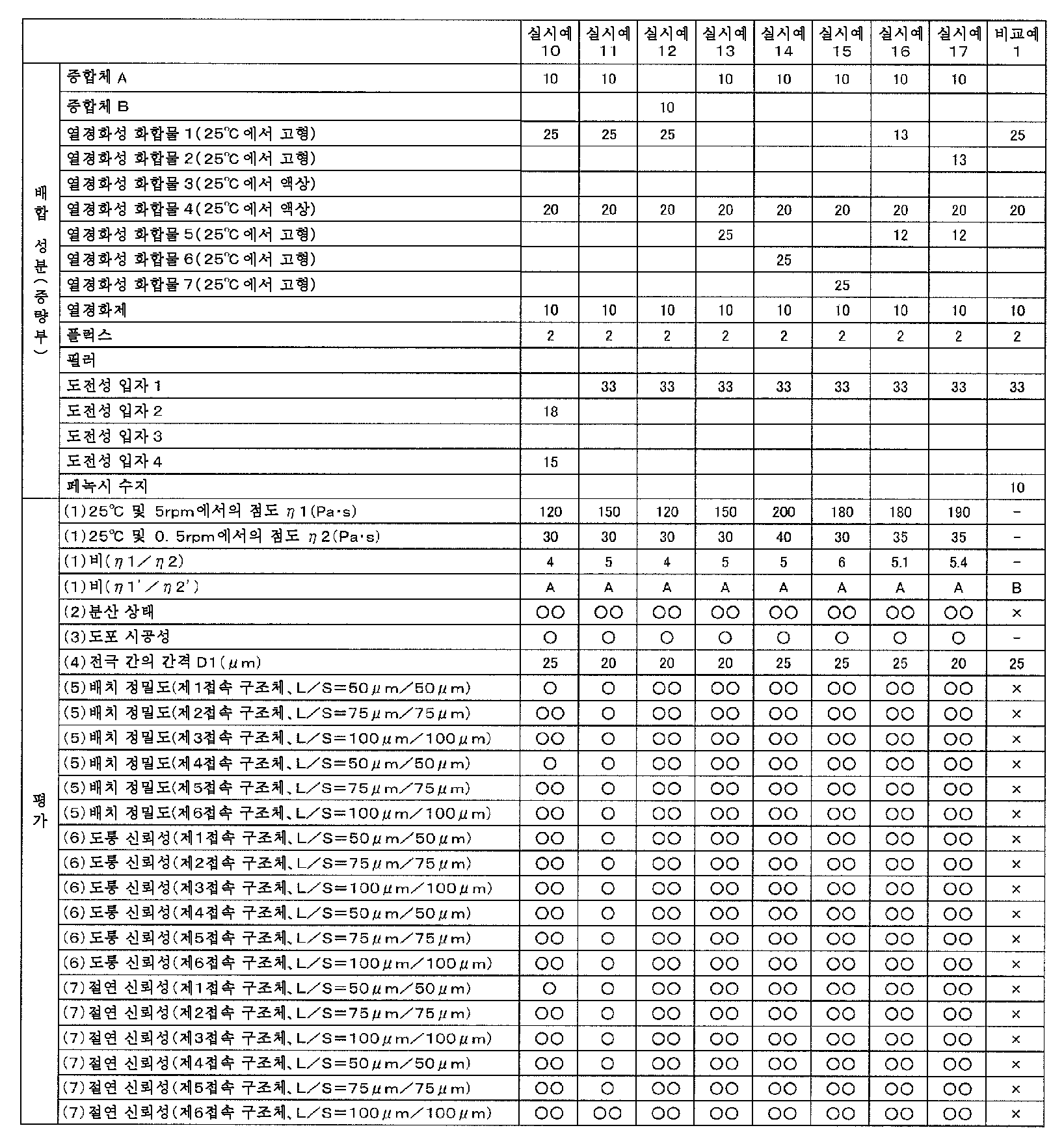
실시예 1과 비교예 1의 결과의 차이와, 실시예 11과 비교예 3의 결과의 차이로부터, 제2 접속 대상 부재가 플렉시블 프린트 기판인 경우에, 제2 접속 대상 부재가 반도체 칩인 경우에 비해, 본 발명의 도전 페이스트의 사용에 의한 도통 신뢰성의 향상 효과가 보다 한층 효과적으로 얻어지는 것을 알 수 있다. 또한, 실시예 16, 17의 도통 신뢰성의 평가(결과 ○○)에서는, 융점이 다른 복수의 25℃에서 고형인 열경화성 화합물을 사용하고 있기 때문에, 다른 실시예의 평가(결과 ○○도 포함함)보다 접속 저항의 구체적인 수치는 낮았다. 실시예 16, 17에서는, 다른 실시예와 비교하여, 도통 신뢰성이 특히 우수하다.From the difference between the results of Example 1 and Comparative Example 1 and the difference between the results of Example 11 and Comparative Example 3, it can be seen that, when the second connection target member is a flexible printed circuit board, , It can be seen that the effect of improving the conduction reliability by using the conductive paste of the present invention can be obtained more effectively. Further, in the evaluation of the conduction reliability (results xxx) of Examples 16 and 17, since a plurality of thermosetting compounds which are solid at 25 占 폚 having different melting points are used, Specific values of connection resistance were low. In Examples 16 and 17, the conduction reliability is particularly excellent as compared with the other embodiments.
1, 1X : 접속 구조체
2 : 제1 접속 대상 부재
2a : 제1 전극
3 : 제2 접속 대상 부재
3a : 제2 전극
4, 4X : 접속부
4A, 4XA : 땜납부
4B, 4XB : 경화물부
11 : 도전 페이스트
11A : 땜납 입자
11B : 열경화성 성분
51 : 도전성 입자
51a : 외표면
52 : 기재 입자
52a : 외표면
53 : 도전부
54 : 제1 도전부
54a : 외표면
55 : 땜납부
61 : 도전성 입자
62 : 땜납부1, 1X: connection structure
2: first connection object member
2a: first electrode
3: second connection object member
3a: second electrode
4, 4X: connection
4A, 4XA: soldering portion
4B and 4XB:
11: Conductive paste
11A: Solder particles
11B: Thermosetting component
51: conductive particles
51a: outer surface
52: Base particles
52a: outer surface
53:
54: first conductive part
54a: outer surface
55: soldering portion
61: conductive particles
62: soldering portion
Claims (18)
상기 열경화성 성분이, 25℃에서 고형인 열경화성 화합물과, 열경화제를 함유하고,
도전 페이스트 중에서, 상기 25℃에서 고형인 열경화성 화합물이 입자상으로 분산되어 있는 도전 페이스트.A thermosetting component and a plurality of conductive particles,
Wherein the thermosetting component comprises a thermosetting compound which is solid at 25 DEG C and a thermosetting agent,
Wherein the thermosetting compound solid at 25 占 폚 is dispersed in the form of particles in the conductive paste.
25℃에서 고형인 열경화성 화합물과 열경화제를 함유하는 열경화성 성분 및 복수의 도전성 입자를 혼합해서 혼합물을 얻고, 다음에 상기 혼합물을, 상기 25℃에서 고형인 열경화성 화합물의 융점 이상이면서 상기 열경화성 성분의 경화 온도 미만으로 가열하여, 상기 25℃에서 고형인 열경화성 화합물을 용융시킨 후에 고화시킴으로써, 상기 25℃에서 고형인 열경화성 화합물이 입자상으로 분산되어 있는 도전 페이스트를 얻거나, 또는
25℃에서 고형인 열경화성 화합물을 입자상으로 한 후에, 입자상이고 또한 25℃에서 고형인 열경화성 화합물과 열경화제를 함유하는 열경화성 성분과, 복수의 도전성 입자를 포함하는 혼합물이고, 또한 상기 25℃에서 고형인 열경화성 화합물이 입자상으로 분산되어 있는 도전 페이스트를 얻는, 도전 페이스트의 제조 방법.A method for producing a conductive paste according to any one of claims 1 to 12,
A mixture of a thermosetting component containing a thermosetting compound which is solid at 25 占 폚 and a thermosetting component and a plurality of conductive particles is obtained by mixing the mixture at 25 占 폚 at a temperature not lower than the melting point of the thermosetting compound which is solid at 25 占 폚, To obtain a conductive paste in which the thermosetting compound solid at 25 占 폚 is dispersed in a particulate form by melting the thermosetting compound solid at 25 占 폚 and then solidifying the thermosetting compound at 25 占 폚,
A mixture containing a plurality of conductive particles and a thermosetting component containing a thermosetting compound and a thermosetting agent which are particulate and solid at 25 DEG C and a thermosetting agent at 25 DEG C at a temperature of 25 DEG C, A conductive paste in which a thermosetting compound is dispersed in particles is obtained.
적어도 1개의 제2 전극을 표면에 갖는 제2 접속 대상 부재와,
상기 제1 접속 대상 부재와 상기 제2 접속 대상 부재를 접속하고 있는 접속부를 구비하며,
상기 접속부가, 제1항 내지 제12항 중 어느 한 항에 기재된 도전 페이스트에 의해 형성되어 있고,
상기 제1 전극과 상기 제2 전극이, 상기 접속부 중의 상기 도전성 입자에 의해 전기적으로 접속되어 있는 접속 구조체.A first connection target member having at least one first electrode on its surface,
A second connection target member having at least one second electrode on its surface,
And a connection unit connecting the first connection target member and the second connection target member,
Wherein the connecting portion is formed by the conductive paste according to any one of claims 1 to 12,
Wherein the first electrode and the second electrode are electrically connected by the conductive particles in the connection portion.
상기 도전 페이스트의 상기 제1 접속 대상 부재측과는 반대인 표면 상에, 적어도 1개의 제2 전극을 표면에 갖는 제2 접속 대상 부재를, 상기 제1 전극과 상기 제2 전극이 대향하도록 배치하는 공정과,
상기 25℃에서 고형인 열경화성 화합물의 융점 이상이면서 상기 열경화성 성분의 경화 온도 이상으로 상기 도전 페이스트를 가열함으로써, 상기 제1 접속 대상 부재와 상기 제2 접속 대상 부재를 접속하고 있는 접속부를 상기 도전 페이스트에 의해 형성하고, 또한 상기 제1 전극과 상기 제2 전극을 상기 접속부 중의 상기 도전성 입자에 의해 전기적으로 접속하는 공정을 구비하는, 접속 구조체의 제조 방법.13. A method of manufacturing a semiconductor device, comprising the steps of: disposing the conductive paste on a surface of a first connection target member having at least one first electrode on a surface thereof using the conductive paste according to any one of claims 1 to 12;
A second connection target member having at least one second electrode on its surface on a surface opposite to the first connection target member side of the conductive paste is arranged so that the first electrode and the second electrode face each other The process,
Heating the conductive paste at a temperature higher than the melting point of the thermosetting compound solid at 25 占 폚 and not lower than the hardening temperature of the thermosetting component to form a connection portion connecting the first connection target member and the second connection target member to the conductive paste And electrically connecting the first electrode and the second electrode by the conductive particles in the connection portion.
Applications Claiming Priority (3)
| Application Number | Priority Date | Filing Date | Title |
|---|---|---|---|
| JPJP-P-2014-100073 | 2014-05-14 | ||
| JP2014100073 | 2014-05-14 | ||
| PCT/JP2015/063095 WO2015174299A1 (en) | 2014-05-14 | 2015-05-01 | Conductive paste, production method for conductive paste, connection structure, and production method for connection structure |
Publications (2)
| Publication Number | Publication Date |
|---|---|
| KR20170007724A true KR20170007724A (en) | 2017-01-20 |
| KR102410173B1 KR102410173B1 (en) | 2022-06-20 |
Family
ID=54479840
Family Applications (1)
| Application Number | Title | Priority Date | Filing Date |
|---|---|---|---|
| KR1020167012326A KR102410173B1 (en) | 2014-05-14 | 2015-05-01 | Conductive paste, production method for conductive paste, connection structure, and production method for connection structure |
Country Status (5)
| Country | Link |
|---|---|
| JP (2) | JP6329144B2 (en) |
| KR (1) | KR102410173B1 (en) |
| CN (1) | CN105849820B (en) |
| TW (1) | TWI672710B (en) |
| WO (1) | WO2015174299A1 (en) |
Families Citing this family (12)
| Publication number | Priority date | Publication date | Assignee | Title |
|---|---|---|---|---|
| JP6966322B2 (en) * | 2016-01-25 | 2021-11-17 | 積水化学工業株式会社 | Conductive materials and connection structures |
| KR102649653B1 (en) * | 2016-02-10 | 2024-03-19 | 가부시끼가이샤 레조낙 | Conductive particles, insulating coated conductive particles, anisotropic conductive adhesive, bonded structure, and manufacturing method of conductive particles |
| JP6623092B2 (en) * | 2016-03-22 | 2019-12-18 | 株式会社巴川製紙所 | Thermosetting adhesive sheet and method for producing the same |
| JP2017191685A (en) * | 2016-04-12 | 2017-10-19 | 積水化学工業株式会社 | Conductive material and connection structure |
| JP6849374B2 (en) * | 2016-10-06 | 2021-03-24 | イー・アイ・デュポン・ドウ・ヌムール・アンド・カンパニーE.I.Du Pont De Nemours And Company | Conductive paste for joining |
| KR20190098709A (en) | 2018-02-14 | 2019-08-22 | 에피스타 코포레이션 | Light-emitting device, manufacturing method thereof and display module using the same |
| JPWO2019181836A1 (en) * | 2018-03-23 | 2021-02-04 | 積水化学工業株式会社 | Conductive particles, conductive materials and connecting structures |
| JP7195779B2 (en) | 2018-06-22 | 2022-12-26 | 株式会社ジャパンディスプレイ | Liquid crystal panel, electro-optical device, and method for manufacturing liquid crystal panel |
| JP7210840B2 (en) | 2018-08-06 | 2023-01-24 | 株式会社レゾナック | Thermosetting composition for forming elastic resin, elastic resin, and semiconductor device |
| TWI819073B (en) | 2019-08-22 | 2023-10-21 | 晶元光電股份有限公司 | Light-emitting device, manufacturing method thereof and display module using the same |
| JP7389657B2 (en) | 2020-01-21 | 2023-11-30 | 積水化学工業株式会社 | Conductive paste and connection structure |
| WO2024048628A1 (en) * | 2022-09-01 | 2024-03-07 | タツタ電線株式会社 | Conductive paste and multilayer substrate using same |
Citations (7)
| Publication number | Priority date | Publication date | Assignee | Title |
|---|---|---|---|---|
| JP2000345010A (en) | 1999-04-01 | 2000-12-12 | Mitsui Chemicals Inc | Anisotropically conductive paste |
| WO2008023452A1 (en) | 2006-08-25 | 2008-02-28 | Sumitomo Bakelite Co., Ltd. | Adhesive tape, joint structure, and semiconductor package |
| JP2011233633A (en) | 2010-04-26 | 2011-11-17 | Hitachi Chem Co Ltd | Circuit connection material, and connection body for circuit member |
| KR20120062682A (en) * | 2009-08-26 | 2012-06-14 | 세키스이가가쿠 고교가부시키가이샤 | Anisotropic conductive material, connection structure, and connection structure producing method |
| JP2012169263A (en) * | 2011-01-24 | 2012-09-06 | Sekisui Chem Co Ltd | Anisotropic conductive material, method for manufacturing connection structure and connection structure |
| JP2013077557A (en) * | 2011-09-13 | 2013-04-25 | Sekisui Chem Co Ltd | Anisotropic conductive material and connection structure |
| JP2014056816A (en) * | 2012-08-10 | 2014-03-27 | Sekisui Chem Co Ltd | Conductive material and connection structure |
Family Cites Families (14)
| Publication number | Priority date | Publication date | Assignee | Title |
|---|---|---|---|---|
| EP1426978A4 (en) * | 2001-08-22 | 2008-09-10 | Sumitomo Electric Industries | Conductive paste and conductive film using it, plating method and production method for fine metal component |
| JP2004043602A (en) * | 2002-07-10 | 2004-02-12 | Bridgestone Corp | Anisotropically conductive film |
| CN101016402A (en) * | 2003-01-07 | 2007-08-15 | 积水化学工业株式会社 | Curing resin composition, adhesive epoxy resin paste, adhesive epoxy resin sheet, conductive connection paste, conductive connection sheet, and electronic component joined body |
| JP4673933B2 (en) * | 2009-08-26 | 2011-04-20 | 積水化学工業株式会社 | Anisotropic conductive material and connection structure |
| JP5498407B2 (en) * | 2011-01-25 | 2014-05-21 | 積水化学工業株式会社 | Method for manufacturing connection structure |
| JP2013023671A (en) * | 2011-07-26 | 2013-02-04 | Sumitomo Electric Ind Ltd | Film-like anisotropic conductive adhesive and inspection method of the same |
| KR101774629B1 (en) * | 2011-08-18 | 2017-09-04 | 세키스이가가쿠 고교가부시키가이샤 | Epoxy compound, epoxy compound mixture, curable composition, and connecting structure |
| CN103843469B (en) * | 2011-09-30 | 2017-05-03 | 株式会社村田制作所 | Electronic device, joining material, and method for producing electronic device |
| KR101391697B1 (en) * | 2011-12-14 | 2014-05-07 | 제일모직주식회사 | Anisotropic conductive film composition and anisotropic conductive film using the composition |
| KR102152473B1 (en) * | 2011-12-16 | 2020-09-04 | 히타치가세이가부시끼가이샤 | Adhesive composition, film-like adhesive, adhesive sheet, connection structure and method for producing connection structure |
| JP5737278B2 (en) * | 2011-12-21 | 2015-06-17 | 日立化成株式会社 | Circuit connection material, connection body, and method of manufacturing connection body |
| US8802989B2 (en) * | 2012-03-26 | 2014-08-12 | Sekisui Chemical Co., Ltd. | Conductive material and connection structure |
| JP6079425B2 (en) * | 2012-05-16 | 2017-02-15 | 日立化成株式会社 | Conductive particles, anisotropic conductive adhesive film, and connection structure |
| WO2014007334A1 (en) * | 2012-07-05 | 2014-01-09 | 積水化学工業株式会社 | Conductive particle, resin particle, conductive material, and connection structure |
-
2015
- 2015-05-01 WO PCT/JP2015/063095 patent/WO2015174299A1/en active Application Filing
- 2015-05-01 JP JP2015524523A patent/JP6329144B2/en active Active
- 2015-05-01 KR KR1020167012326A patent/KR102410173B1/en active IP Right Grant
- 2015-05-01 CN CN201580003105.5A patent/CN105849820B/en active Active
- 2015-05-13 TW TW104115298A patent/TWI672710B/en active
-
2016
- 2016-10-27 JP JP2016210379A patent/JP2017063038A/en active Pending
Patent Citations (7)
| Publication number | Priority date | Publication date | Assignee | Title |
|---|---|---|---|---|
| JP2000345010A (en) | 1999-04-01 | 2000-12-12 | Mitsui Chemicals Inc | Anisotropically conductive paste |
| WO2008023452A1 (en) | 2006-08-25 | 2008-02-28 | Sumitomo Bakelite Co., Ltd. | Adhesive tape, joint structure, and semiconductor package |
| KR20120062682A (en) * | 2009-08-26 | 2012-06-14 | 세키스이가가쿠 고교가부시키가이샤 | Anisotropic conductive material, connection structure, and connection structure producing method |
| JP2011233633A (en) | 2010-04-26 | 2011-11-17 | Hitachi Chem Co Ltd | Circuit connection material, and connection body for circuit member |
| JP2012169263A (en) * | 2011-01-24 | 2012-09-06 | Sekisui Chem Co Ltd | Anisotropic conductive material, method for manufacturing connection structure and connection structure |
| JP2013077557A (en) * | 2011-09-13 | 2013-04-25 | Sekisui Chem Co Ltd | Anisotropic conductive material and connection structure |
| JP2014056816A (en) * | 2012-08-10 | 2014-03-27 | Sekisui Chem Co Ltd | Conductive material and connection structure |
Also Published As
| Publication number | Publication date |
|---|---|
| CN105849820A (en) | 2016-08-10 |
| KR102410173B1 (en) | 2022-06-20 |
| JP6329144B2 (en) | 2018-05-23 |
| JPWO2015174299A1 (en) | 2017-04-20 |
| WO2015174299A1 (en) | 2015-11-19 |
| TWI672710B (en) | 2019-09-21 |
| CN105849820B (en) | 2018-10-26 |
| TW201601170A (en) | 2016-01-01 |
| JP2017063038A (en) | 2017-03-30 |
Similar Documents
| Publication | Publication Date | Title |
|---|---|---|
| KR20170007724A (en) | Conductive paste, production method for conductive paste, connection structure, and production method for connection structure | |
| JP5819026B1 (en) | Method for manufacturing connection structure | |
| KR102392995B1 (en) | Conductive paste, connected structure and method for producing connected structure | |
| KR102411356B1 (en) | Electrically conductive paste, joined structure, and method for manufacturing joined structure | |
| WO2015125778A1 (en) | Conductive paste, connection structure, and connection structure manufacturing method | |
| JP6325923B2 (en) | Conductive material and connection structure | |
| KR102393302B1 (en) | Conductive paste, connection structure, and production method for connection structure | |
| WO2016104275A1 (en) | Electrically conductive paste, connection structure, and production method for connection structure | |
| WO2016104276A1 (en) | Electrically conductive paste, connection structure, and production method for connection structure | |
| JP7277289B2 (en) | Conductive material, connection structure, and method for manufacturing connection structure | |
| WO2016013474A1 (en) | Method for producing connection structure | |
| JP6514610B2 (en) | Method of manufacturing connection structure | |
| JP6514615B2 (en) | Method of manufacturing connection structure | |
| JP2016004972A (en) | Connection structure and manufacturing method for the same | |
| WO2016035637A1 (en) | Method of manufacturing connection structure | |
| KR20180029945A (en) | Conductive material and connection structure | |
| JP2017017318A (en) | Connection structure manufacturing method and connection structure | |
| JP2020170591A (en) | Conductive material and connection structure | |
| JP2017022099A (en) | Conductive material and connection structure |
Legal Events
| Date | Code | Title | Description |
|---|---|---|---|
| E902 | Notification of reason for refusal | ||
| AMND | Amendment | ||
| E601 | Decision to refuse application | ||
| X091 | Application refused [patent] | ||
| AMND | Amendment | ||
| X701 | Decision to grant (after re-examination) | ||
| GRNT | Written decision to grant |