KR20160123322A - Low-Profile Package with Passive Device - Google Patents
Low-Profile Package with Passive Device Download PDFInfo
- Publication number
- KR20160123322A KR20160123322A KR1020167024477A KR20167024477A KR20160123322A KR 20160123322 A KR20160123322 A KR 20160123322A KR 1020167024477 A KR1020167024477 A KR 1020167024477A KR 20167024477 A KR20167024477 A KR 20167024477A KR 20160123322 A KR20160123322 A KR 20160123322A
- Authority
- KR
- South Korea
- Prior art keywords
- substrate
- recess
- interconnect
- vias
- thickness
- Prior art date
Links
- 239000000758 substrate Substances 0.000 claims abstract description 242
- 229910000679 solder Inorganic materials 0.000 claims description 65
- 238000000034 method Methods 0.000 claims description 35
- 239000004020 conductor Substances 0.000 claims description 28
- 239000011521 glass Substances 0.000 claims description 19
- 239000003990 capacitor Substances 0.000 claims description 17
- 239000002184 metal Substances 0.000 claims description 17
- 229910052751 metal Inorganic materials 0.000 claims description 17
- 230000008878 coupling Effects 0.000 claims description 11
- 238000010168 coupling process Methods 0.000 claims description 11
- 238000005859 coupling reaction Methods 0.000 claims description 11
- 238000002161 passivation Methods 0.000 claims description 8
- 239000004065 semiconductor Substances 0.000 claims description 8
- RYGMFSIKBFXOCR-UHFFFAOYSA-N Copper Chemical compound [Cu] RYGMFSIKBFXOCR-UHFFFAOYSA-N 0.000 claims description 4
- 229910052802 copper Inorganic materials 0.000 claims description 4
- 239000010949 copper Substances 0.000 claims description 4
- 238000004891 communication Methods 0.000 claims description 2
- 238000005530 etching Methods 0.000 claims description 2
- 238000000059 patterning Methods 0.000 claims 5
- 238000007598 dipping method Methods 0.000 claims 1
- 230000005226 mechanical processes and functions Effects 0.000 claims 1
- 238000004519 manufacturing process Methods 0.000 description 12
- PXHVJJICTQNCMI-UHFFFAOYSA-N Nickel Chemical compound [Ni] PXHVJJICTQNCMI-UHFFFAOYSA-N 0.000 description 6
- 230000008569 process Effects 0.000 description 5
- 230000008901 benefit Effects 0.000 description 3
- 238000013461 design Methods 0.000 description 3
- 229910052759 nickel Inorganic materials 0.000 description 3
- 230000003071 parasitic effect Effects 0.000 description 3
- 239000000853 adhesive Substances 0.000 description 2
- 230000001070 adhesive effect Effects 0.000 description 2
- 238000005336 cracking Methods 0.000 description 2
- 238000000151 deposition Methods 0.000 description 2
- 238000010586 diagram Methods 0.000 description 2
- 238000005553 drilling Methods 0.000 description 2
- 239000000463 material Substances 0.000 description 2
- 150000002739 metals Chemical class 0.000 description 2
- 238000012546 transfer Methods 0.000 description 2
- 239000004952 Polyamide Substances 0.000 description 1
- 229910052581 Si3N4 Inorganic materials 0.000 description 1
- 230000004888 barrier function Effects 0.000 description 1
- 230000009286 beneficial effect Effects 0.000 description 1
- 230000015572 biosynthetic process Effects 0.000 description 1
- 239000000969 carrier Substances 0.000 description 1
- 230000001413 cellular effect Effects 0.000 description 1
- 230000007423 decrease Effects 0.000 description 1
- 230000008021 deposition Effects 0.000 description 1
- 238000001312 dry etching Methods 0.000 description 1
- 238000009713 electroplating Methods 0.000 description 1
- 230000007613 environmental effect Effects 0.000 description 1
- 238000012986 modification Methods 0.000 description 1
- 230000004048 modification Effects 0.000 description 1
- 229920000620 organic polymer Polymers 0.000 description 1
- 238000001020 plasma etching Methods 0.000 description 1
- 238000007747 plating Methods 0.000 description 1
- 229920002647 polyamide Polymers 0.000 description 1
- 229920000642 polymer Polymers 0.000 description 1
- 238000012545 processing Methods 0.000 description 1
- 230000009467 reduction Effects 0.000 description 1
- 238000004904 shortening Methods 0.000 description 1
- 229910052710 silicon Inorganic materials 0.000 description 1
- 239000010703 silicon Substances 0.000 description 1
- HQVNEWCFYHHQES-UHFFFAOYSA-N silicon nitride Chemical compound N12[Si]34N5[Si]62N3[Si]51N64 HQVNEWCFYHHQES-UHFFFAOYSA-N 0.000 description 1
- 238000006467 substitution reaction Methods 0.000 description 1
- XLYOFNOQVPJJNP-UHFFFAOYSA-N water Substances O XLYOFNOQVPJJNP-UHFFFAOYSA-N 0.000 description 1
- 238000001039 wet etching Methods 0.000 description 1
- 238000004804 winding Methods 0.000 description 1
Images


Classifications
-
- H—ELECTRICITY
- H05—ELECTRIC TECHNIQUES NOT OTHERWISE PROVIDED FOR
- H05K—PRINTED CIRCUITS; CASINGS OR CONSTRUCTIONAL DETAILS OF ELECTRIC APPARATUS; MANUFACTURE OF ASSEMBLAGES OF ELECTRICAL COMPONENTS
- H05K1/00—Printed circuits
- H05K1/18—Printed circuits structurally associated with non-printed electric components
- H05K1/182—Printed circuits structurally associated with non-printed electric components associated with components mounted in the printed circuit board, e.g. insert mounted components [IMC]
-
- H—ELECTRICITY
- H01—ELECTRIC ELEMENTS
- H01F—MAGNETS; INDUCTANCES; TRANSFORMERS; SELECTION OF MATERIALS FOR THEIR MAGNETIC PROPERTIES
- H01F17/00—Fixed inductances of the signal type
- H01F17/0006—Printed inductances
-
- H—ELECTRICITY
- H01—ELECTRIC ELEMENTS
- H01L—SEMICONDUCTOR DEVICES NOT COVERED BY CLASS H10
- H01L21/00—Processes or apparatus adapted for the manufacture or treatment of semiconductor or solid state devices or of parts thereof
- H01L21/02—Manufacture or treatment of semiconductor devices or of parts thereof
- H01L21/04—Manufacture or treatment of semiconductor devices or of parts thereof the devices having at least one potential-jump barrier or surface barrier, e.g. PN junction, depletion layer or carrier concentration layer
- H01L21/48—Manufacture or treatment of parts, e.g. containers, prior to assembly of the devices, using processes not provided for in a single one of the subgroups H01L21/06 - H01L21/326
- H01L21/4814—Conductive parts
- H01L21/4846—Leads on or in insulating or insulated substrates, e.g. metallisation
- H01L21/4853—Connection or disconnection of other leads to or from a metallisation, e.g. pins, wires, bumps
-
- H—ELECTRICITY
- H01—ELECTRIC ELEMENTS
- H01L—SEMICONDUCTOR DEVICES NOT COVERED BY CLASS H10
- H01L21/00—Processes or apparatus adapted for the manufacture or treatment of semiconductor or solid state devices or of parts thereof
- H01L21/02—Manufacture or treatment of semiconductor devices or of parts thereof
- H01L21/04—Manufacture or treatment of semiconductor devices or of parts thereof the devices having at least one potential-jump barrier or surface barrier, e.g. PN junction, depletion layer or carrier concentration layer
- H01L21/48—Manufacture or treatment of parts, e.g. containers, prior to assembly of the devices, using processes not provided for in a single one of the subgroups H01L21/06 - H01L21/326
- H01L21/4814—Conductive parts
- H01L21/4846—Leads on or in insulating or insulated substrates, e.g. metallisation
- H01L21/486—Via connections through the substrate with or without pins
-
- H—ELECTRICITY
- H01—ELECTRIC ELEMENTS
- H01L—SEMICONDUCTOR DEVICES NOT COVERED BY CLASS H10
- H01L23/00—Details of semiconductor or other solid state devices
- H01L23/12—Mountings, e.g. non-detachable insulating substrates
- H01L23/13—Mountings, e.g. non-detachable insulating substrates characterised by the shape
-
- H—ELECTRICITY
- H01—ELECTRIC ELEMENTS
- H01L—SEMICONDUCTOR DEVICES NOT COVERED BY CLASS H10
- H01L23/00—Details of semiconductor or other solid state devices
- H01L23/48—Arrangements for conducting electric current to or from the solid state body in operation, e.g. leads, terminal arrangements ; Selection of materials therefor
- H01L23/488—Arrangements for conducting electric current to or from the solid state body in operation, e.g. leads, terminal arrangements ; Selection of materials therefor consisting of soldered or bonded constructions
- H01L23/498—Leads, i.e. metallisations or lead-frames on insulating substrates, e.g. chip carriers
- H01L23/49811—Additional leads joined to the metallisation on the insulating substrate, e.g. pins, bumps, wires, flat leads
-
- H—ELECTRICITY
- H01—ELECTRIC ELEMENTS
- H01L—SEMICONDUCTOR DEVICES NOT COVERED BY CLASS H10
- H01L23/00—Details of semiconductor or other solid state devices
- H01L23/48—Arrangements for conducting electric current to or from the solid state body in operation, e.g. leads, terminal arrangements ; Selection of materials therefor
- H01L23/488—Arrangements for conducting electric current to or from the solid state body in operation, e.g. leads, terminal arrangements ; Selection of materials therefor consisting of soldered or bonded constructions
- H01L23/498—Leads, i.e. metallisations or lead-frames on insulating substrates, e.g. chip carriers
- H01L23/49827—Via connections through the substrates, e.g. pins going through the substrate, coaxial cables
-
- H—ELECTRICITY
- H01—ELECTRIC ELEMENTS
- H01L—SEMICONDUCTOR DEVICES NOT COVERED BY CLASS H10
- H01L23/00—Details of semiconductor or other solid state devices
- H01L23/48—Arrangements for conducting electric current to or from the solid state body in operation, e.g. leads, terminal arrangements ; Selection of materials therefor
- H01L23/488—Arrangements for conducting electric current to or from the solid state body in operation, e.g. leads, terminal arrangements ; Selection of materials therefor consisting of soldered or bonded constructions
- H01L23/498—Leads, i.e. metallisations or lead-frames on insulating substrates, e.g. chip carriers
- H01L23/49866—Leads, i.e. metallisations or lead-frames on insulating substrates, e.g. chip carriers characterised by the materials
- H01L23/49894—Materials of the insulating layers or coatings
-
- H—ELECTRICITY
- H01—ELECTRIC ELEMENTS
- H01L—SEMICONDUCTOR DEVICES NOT COVERED BY CLASS H10
- H01L28/00—Passive two-terminal components without a potential-jump or surface barrier for integrated circuits; Details thereof; Multistep manufacturing processes therefor
- H01L28/10—Inductors
-
- H—ELECTRICITY
- H05—ELECTRIC TECHNIQUES NOT OTHERWISE PROVIDED FOR
- H05K—PRINTED CIRCUITS; CASINGS OR CONSTRUCTIONAL DETAILS OF ELECTRIC APPARATUS; MANUFACTURE OF ASSEMBLAGES OF ELECTRICAL COMPONENTS
- H05K1/00—Printed circuits
- H05K1/02—Details
- H05K1/03—Use of materials for the substrate
- H05K1/0306—Inorganic insulating substrates, e.g. ceramic, glass
-
- H—ELECTRICITY
- H05—ELECTRIC TECHNIQUES NOT OTHERWISE PROVIDED FOR
- H05K—PRINTED CIRCUITS; CASINGS OR CONSTRUCTIONAL DETAILS OF ELECTRIC APPARATUS; MANUFACTURE OF ASSEMBLAGES OF ELECTRICAL COMPONENTS
- H05K1/00—Printed circuits
- H05K1/02—Details
- H05K1/11—Printed elements for providing electric connections to or between printed circuits
- H05K1/115—Via connections; Lands around holes or via connections
-
- H—ELECTRICITY
- H05—ELECTRIC TECHNIQUES NOT OTHERWISE PROVIDED FOR
- H05K—PRINTED CIRCUITS; CASINGS OR CONSTRUCTIONAL DETAILS OF ELECTRIC APPARATUS; MANUFACTURE OF ASSEMBLAGES OF ELECTRICAL COMPONENTS
- H05K1/00—Printed circuits
- H05K1/16—Printed circuits incorporating printed electric components, e.g. printed resistor, capacitor, inductor
- H05K1/165—Printed circuits incorporating printed electric components, e.g. printed resistor, capacitor, inductor incorporating printed inductors
-
- H—ELECTRICITY
- H05—ELECTRIC TECHNIQUES NOT OTHERWISE PROVIDED FOR
- H05K—PRINTED CIRCUITS; CASINGS OR CONSTRUCTIONAL DETAILS OF ELECTRIC APPARATUS; MANUFACTURE OF ASSEMBLAGES OF ELECTRICAL COMPONENTS
- H05K3/00—Apparatus or processes for manufacturing printed circuits
- H05K3/40—Forming printed elements for providing electric connections to or between printed circuits
- H05K3/4038—Through-connections; Vertical interconnect access [VIA] connections
-
- H—ELECTRICITY
- H01—ELECTRIC ELEMENTS
- H01L—SEMICONDUCTOR DEVICES NOT COVERED BY CLASS H10
- H01L23/00—Details of semiconductor or other solid state devices
- H01L23/48—Arrangements for conducting electric current to or from the solid state body in operation, e.g. leads, terminal arrangements ; Selection of materials therefor
- H01L23/488—Arrangements for conducting electric current to or from the solid state body in operation, e.g. leads, terminal arrangements ; Selection of materials therefor consisting of soldered or bonded constructions
- H01L23/498—Leads, i.e. metallisations or lead-frames on insulating substrates, e.g. chip carriers
- H01L23/49811—Additional leads joined to the metallisation on the insulating substrate, e.g. pins, bumps, wires, flat leads
- H01L23/49816—Spherical bumps on the substrate for external connection, e.g. ball grid arrays [BGA]
-
- H—ELECTRICITY
- H01—ELECTRIC ELEMENTS
- H01L—SEMICONDUCTOR DEVICES NOT COVERED BY CLASS H10
- H01L2924/00—Indexing scheme for arrangements or methods for connecting or disconnecting semiconductor or solid-state bodies as covered by H01L24/00
- H01L2924/15—Details of package parts other than the semiconductor or other solid state devices to be connected
- H01L2924/151—Die mounting substrate
- H01L2924/1515—Shape
- H01L2924/15158—Shape the die mounting substrate being other than a cuboid
- H01L2924/15159—Side view
-
- H—ELECTRICITY
- H01—ELECTRIC ELEMENTS
- H01L—SEMICONDUCTOR DEVICES NOT COVERED BY CLASS H10
- H01L2924/00—Indexing scheme for arrangements or methods for connecting or disconnecting semiconductor or solid-state bodies as covered by H01L24/00
- H01L2924/15—Details of package parts other than the semiconductor or other solid state devices to be connected
- H01L2924/151—Die mounting substrate
- H01L2924/153—Connection portion
- H01L2924/1531—Connection portion the connection portion being formed only on the surface of the substrate opposite to the die mounting surface
- H01L2924/15311—Connection portion the connection portion being formed only on the surface of the substrate opposite to the die mounting surface being a ball array, e.g. BGA
-
- H—ELECTRICITY
- H01—ELECTRIC ELEMENTS
- H01L—SEMICONDUCTOR DEVICES NOT COVERED BY CLASS H10
- H01L2924/00—Indexing scheme for arrangements or methods for connecting or disconnecting semiconductor or solid-state bodies as covered by H01L24/00
- H01L2924/15—Details of package parts other than the semiconductor or other solid state devices to be connected
- H01L2924/151—Die mounting substrate
- H01L2924/156—Material
- H01L2924/157—Material with a principal constituent of the material being a metal or a metalloid, e.g. boron [B], silicon [Si], germanium [Ge], arsenic [As], antimony [Sb], tellurium [Te] and polonium [Po], and alloys thereof
-
- H—ELECTRICITY
- H01—ELECTRIC ELEMENTS
- H01L—SEMICONDUCTOR DEVICES NOT COVERED BY CLASS H10
- H01L2924/00—Indexing scheme for arrangements or methods for connecting or disconnecting semiconductor or solid-state bodies as covered by H01L24/00
- H01L2924/15—Details of package parts other than the semiconductor or other solid state devices to be connected
- H01L2924/151—Die mounting substrate
- H01L2924/156—Material
- H01L2924/15786—Material with a principal constituent of the material being a non metallic, non metalloid inorganic material
- H01L2924/15788—Glasses, e.g. amorphous oxides, nitrides or fluorides
-
- H—ELECTRICITY
- H05—ELECTRIC TECHNIQUES NOT OTHERWISE PROVIDED FOR
- H05K—PRINTED CIRCUITS; CASINGS OR CONSTRUCTIONAL DETAILS OF ELECTRIC APPARATUS; MANUFACTURE OF ASSEMBLAGES OF ELECTRICAL COMPONENTS
- H05K2201/00—Indexing scheme relating to printed circuits covered by H05K1/00
- H05K2201/10—Details of components or other objects attached to or integrated in a printed circuit board
- H05K2201/10007—Types of components
- H05K2201/10015—Non-printed capacitor
-
- H—ELECTRICITY
- H05—ELECTRIC TECHNIQUES NOT OTHERWISE PROVIDED FOR
- H05K—PRINTED CIRCUITS; CASINGS OR CONSTRUCTIONAL DETAILS OF ELECTRIC APPARATUS; MANUFACTURE OF ASSEMBLAGES OF ELECTRICAL COMPONENTS
- H05K2201/00—Indexing scheme relating to printed circuits covered by H05K1/00
- H05K2201/10—Details of components or other objects attached to or integrated in a printed circuit board
- H05K2201/10227—Other objects, e.g. metallic pieces
- H05K2201/10242—Metallic cylinders
-
- H—ELECTRICITY
- H05—ELECTRIC TECHNIQUES NOT OTHERWISE PROVIDED FOR
- H05K—PRINTED CIRCUITS; CASINGS OR CONSTRUCTIONAL DETAILS OF ELECTRIC APPARATUS; MANUFACTURE OF ASSEMBLAGES OF ELECTRICAL COMPONENTS
- H05K2201/00—Indexing scheme relating to printed circuits covered by H05K1/00
- H05K2201/10—Details of components or other objects attached to or integrated in a printed circuit board
- H05K2201/10613—Details of electrical connections of non-printed components, e.g. special leads
- H05K2201/10954—Other details of electrical connections
- H05K2201/10984—Component carrying a connection agent, e.g. solder, adhesive
-
- Y—GENERAL TAGGING OF NEW TECHNOLOGICAL DEVELOPMENTS; GENERAL TAGGING OF CROSS-SECTIONAL TECHNOLOGIES SPANNING OVER SEVERAL SECTIONS OF THE IPC; TECHNICAL SUBJECTS COVERED BY FORMER USPC CROSS-REFERENCE ART COLLECTIONS [XRACs] AND DIGESTS
- Y10—TECHNICAL SUBJECTS COVERED BY FORMER USPC
- Y10T—TECHNICAL SUBJECTS COVERED BY FORMER US CLASSIFICATION
- Y10T29/00—Metal working
- Y10T29/49—Method of mechanical manufacture
- Y10T29/49002—Electrical device making
- Y10T29/49117—Conductor or circuit manufacturing
- Y10T29/49124—On flat or curved insulated base, e.g., printed circuit, etc.
- Y10T29/49155—Manufacturing circuit on or in base
- Y10T29/49165—Manufacturing circuit on or in base by forming conductive walled aperture in base
Abstract
대응하는 상호접속부들을 수용하는 복수의 리세스들을 포함하는 로우-프로파일 패시브-온-패키지가 제공된다. 리세스들 내의 상호접속부들의 수용 때문에, 패시브-온-패키지는, 기판에 대한 두께와 상호접속부 높이 또는 직경의 합보다 작은 높이를 갖는다.There is provided a low-profile passive-on-package comprising a plurality of recesses for receiving corresponding interconnections. Because of the acceptance of the interconnections in the recesses, the passive-on-package has a height that is less than the sum of the thickness and interconnect height or diameter for the substrate.
Description
관련 출원들의 교차 참조Cross reference of related applications
[0001] 본 출원은, 2014년 2월 18일에 출원된 미국 가특허 출원 시리얼 넘버 제61/941,308호의 출원일을 우선권으로 주장하고, 2014년 3월 7일에 출원된 미국 특허 출원 시리얼 넘버 제 14/200,684호의 출원일을 우선권으로 주장하며, 상기 출원 둘 모두는 그 전체가 인용에 의해 본원에 포함된다. [0001] This application claims the benefit of U.S. Provisional Patent Application Ser. No. 61 / 941,308, filed Feb. 18, 2014, which claims the priority of U.S. Patent Application Serial No. 14 / 200,684 filed on Mar. 7, The filing date of which is hereby incorporated by reference in its entirety.
[0002] 본 출원은 집적 회로 패키지 기판들에 관한 것으로, 보다 구체적으로, 패시브 디바이스를 구비한 로우-프로파일(low-profile) 패키지에 관한 것이다.[0002] The present application relates to integrated circuit package substrates, and more particularly, to a low-profile package with passive devices.
[0003] POG(passive-on-glass) 패키지에서, 인덕터들 및 커패시터들과 같은 패시브 컴포넌트들이 유리 기판에 통합된다. 이후, PoG 패키지는 무선 주파수(RF) 프런트 엔드와 같은 완전한 작업 디바이스를 형성하기 위해 반도체 패키지들과 함께 회로 기판에 결합될 수 있다. 회로 기판에 대한 별개의 패시브 디바이스들의 종래의 결합과 비교하여, PoG 패키지의 사용은 훨씬 더 콤팩트하다. 이외에도, PoG 패키지는 전자 시스템용 활성 디바이스들을 포함하는 다이들에 패시브 디바이스들을 통합시키는 것보다 더 저렴한데, 이는 유리 기판들이 결정질 반도체 기판들에 비해 상대적으로 더 저렴하기 때문이다.[0003] In a passive-on-glass (POG) package, passive components such as inductors and capacitors are integrated into the glass substrate. The PoG package can then be coupled to the circuit board together with the semiconductor packages to form a complete working device, such as a radio frequency (RF) front end. Compared to the conventional combination of separate passive devices for circuit boards, the use of PoG packages is much more compact. In addition, the PoG package is cheaper than integrating passive devices into dies containing active devices for electronic systems because glass substrates are relatively inexpensive relative to crystalline semiconductor substrates.
[0004] 이와 같이, POG 패키지가 전자 시스템에 패시브 컴포넌트들을 제공하기 위한 매력적인 대안이지만, PoG 설계는 다수의 과제들에 직면해 있다. 특히, 모바일 디바이스들에 포함되는 전자장치의 크기들을 감소시킬 필요성이 계속해서 증가하고 있다. 사용자가 보다 컴팩트한 디바이스들을 요구함에 따라, 디바이스들 내에 포함된 전자장치는 그에 따라 크기를 수축시켜야 한다. PoG 패키지를 위해 수축시켜야 할 치수들 중 하나는 하부 회로 기판에 대한 그 높이이다. PoG 패키지 높이를 감소시키는 간단한 방법은 그 유리 기판의 두께를 감소시키는 것이다. 그러나 유리는 본질적으로 취성(brittle)이다. 따라서, 유리 기판의 두께가 150 또는 100 마이크론 미만과 같이 과도하게 감소될 경우 유리 기판에 크랙이 발생하기 쉽다. 이러한 기판들이 또한 취성이며, 지나치게 얇은 경우 너무 부서지기 쉽기 때문에 패시브 컴포넌트들이 대신에 반도체 기판에 통합되더라도 문제가 없어지는 것은 아니다. 패시브 컴포넌트들을 지지하기 위해 사용되는 기판의 타입과 관계없이 문제들은 대부분 동일하기 때문에, 용어 "패시브-온-패키지"는 유리, 반도체, 또는 유기 기판 상에 통합되는 패시브 컴포넌트들을 포함하는 패키지를 나타내는 데 사용된다.[0004] Thus, although the POG package is an attractive alternative to providing passive components in electronic systems, the PoG design faces a number of challenges. In particular, there is a continuing need to reduce the sizes of electronic devices included in mobile devices. As the user requires more compact devices, the electronic devices included in the devices must shrink the size accordingly. One of the dimensions to shrink for the PoG package is its height relative to the lower circuit board. A simple way to reduce the PoG package height is to reduce the thickness of the glass substrate. However, glass is intrinsically brittle. Therefore, when the thickness of the glass substrate is excessively reduced to 150 or less than 100 microns, cracks are likely to occur in the glass substrate. Since these substrates are also brittle and too thin to be too brittle, the problem does not disappear even if the passive components are integrated into the semiconductor substrate instead. Since the problems are largely the same regardless of the type of substrate used to support passive components, the term "passive-on-package" refers to a package comprising passive components integrated onto a glass, semiconductor, or organic substrate Is used.
[0005] 유리 기판의 두께를 감소시키는 다른 문제점은 유리 기판 내에 관통-기판 비아들에 의해 형성되는 임베딩된 인덕터들에 대한 인덕턴스이다. 각각의 임베딩된 인덕터에 대한 코일 또는 루프가 한 쌍(또는 그 이상 쌍)의 관통-기판 비아들에 의해 형성된다. 예를 들어, 임베딩된 인덕터 내의 제 1 관통-기판 비아가, 기판의 제 1 표면으로부터 기판에 대한 반대쪽 제 2 표면 상에 형성되는 리드 또는 도체까지 연장될 수 있다. 도체는 또한, 제 2 표면으로부터 제 1 표면으로 다시 연장되는, 임베딩된 인덕터 내의 제 2 관통-기판 비아에 결합된다. 이와 같이, 제 1 표면으로부터 제 1 관통-기판 비아 안으로 진입하는 전류가 제 2 표면 상의 도체를 통해 흘러 제 2 관통-기판 비아 내의 제 1 표면까지 다시 아래로 루핑할 것이다. 이 전류 루프는 결과적으로 발생되는 임베딩된 인덕터에 인덕턴스를 제공한다. 인덕턴스는 (다른 요인들 중에서도) 전류 루프에 의해 에워싸이게 되는 면적에 의존한다. 관통-기판 비아 길이들이 기판을 얇게 하는 만큼 감소되는 경우, 임베딩된 인덕터에 대한 결과적인 인덕턴스도 줄어들 것이다. 기판에 대한 두께가 감소됨에 따라, 이러한 감소된 두께의 기판을 통과하는 관통-기판 비아들의 높이의 길이도 물로 그에 따라 감소된다. 예를 들어, 두께가 200 마이크론인 기판은, 이러한 두께를 통해 연장되고, 따라서 200 마이크론의 대응하는 길이를 갖는 관통-기판 비아들을 가질 수 있다. 하지만, 기판이 단지 100 마이크론의 두께라면, 관통-기판 비아들은 단지 100 마이크론의 길이를 가질 것이다. PoG 패키지에 대한 패키지 높이를 감소시키는 것은 이와 같이 그의 인덕터들에 대한 인덕턴스들을 감소시키는 경향이 있을 것이다. 따라서, 필수 인덕턴스 또한 PoG 패키지 높이들을 감소시키는 장벽이다.[0005] Another problem of reducing the thickness of the glass substrate is the inductance for the embedded inductors formed by the through-substrate vias in the glass substrate. A coil or loop for each embedded inductor is formed by a pair (or more pairs) of through-substrate vias. For example, a first through-substrate via in an embedded inductor may extend from a first surface of the substrate to a lead or conductor formed on a second surface opposite the substrate. The conductor is also coupled to the second through-substrate via in the embedded inductor, extending back from the second surface to the first surface. As such, an electrical current entering the first through-via vias from the first surface will flow through the conductors on the second surface and loop back down to the first surface in the second through-via vias. This current loop provides the resulting inducted inductance to the embedded inductor. The inductance depends on the area enclosed by the current loop (among other factors). If the through-substrate via lengths are reduced by thinning the substrate, the resulting inductance for the embedded inductor will also be reduced. As the thickness for the substrate is reduced, the length of the height of the through-substrate vias through the substrate of this reduced thickness is also reduced accordingly to the water. For example, a substrate with a thickness of 200 microns may extend through this thickness and thus have through-substrate vias with corresponding lengths of 200 microns. However, if the substrate is only 100 microns thick, the through-substrate vias will have a length of only 100 microns. Reducing the package height for a PoG package will thus tend to reduce inductances for its inductors. Thus, the required inductance is also a barrier to reduce PoG package heights.
[0006]
솔더 볼들 또는 패시브-온-패키지를 하부 회로 보드에 결합시키는 상호접속부들의 다른 타입들은 패시브-온-패키지 높이 감소를 제한하는 다른 팩터이다. 패시브-온- 패키지 설계에 있어서의 이러한 과제들을 더 잘 예시하기 위해서, 종래의 패시브-온-패키지(100)가 도 1에 도시된다. 패키지(100)는, 기판(104)에 대한 두께(T)뿐만 아니라 복수의 솔더 볼들(112) 각각에 대한 직경(d1)에 의존하는 하부 회로 보드(미도시)에 관한 두께 또는 높이(H1)를 갖는다. 기판(104)은 기판(104)의 보드-대향쪽 표면(108)로부터 반대쪽 표면(106)에 결합하는 복수의 관통-기판 비아들(102)을 포함한다. 비아들(102)은 임베딩된 인덕터(103)와 같은 3차원 패시브 구조들을 형성할 수 있다. 상술한 바와 같이, 기판(104)에 대한 두께(T)가 감소됨에 따라, 임베딩된 인덕터(103)에 대한 인덕턴스가 감소한다. 솔더 볼들(112)이 표면(108) 상의 대응하는 패드들(110)에 결합한다. 솔더 볼들(112)이 표면(108) 상의 패드들(110)으로부터 프로젝트되기 때문에, 솔더 볼들(112)의 직경(d1)이 감소됨에 따라, 패키지(100)에 대한 높이(H1)가 그에 따라 감소될 것이라는 것을 즉시 인식할 수 있다. 그러나, 솔더 볼들(112)은, 직경(d1)이 과도하게 감소되면 크랙이 발생하기 쉽다. 특히, 종래의 납-함유 솔더의 사용에 의해 제기되는 환경 문제들로 인해 현재 시스템들에서는 무연 솔더가 요구된다. 그러나, 무연 솔더는 통상적으로 종래의 솔더보다 더 취성이므로, 그의 사용은 솔더 볼들(112)에 대해 특정한 최소 직경을 요구한다. 기판(104)의 두께(T) 및 솔더 볼들(112)에 대한 직경(d1) 둘 모두는 따라서, 강도 및 보드 레벨 신뢰도(BLR; board level reliability)뿐만 아니라 인덕터(103)에 대한 필수 인덕턴스를 희생시키지 않고 과도하게 감소될 수 없다. 이와 같이, 높이(H1)는 종래의 패시브-온-패키지들에 대한 이러한 최소 값들을 만족해야 한다. 이 최소 높이 요건은 패키지(100)를 포함하는 시스템들의 결과적인 밀도를 감소시킨다.[0006] Other types of interconnects for bonding solder balls or passive-on-package to a lower circuit board are other factors that limit passive-on-package height reduction. To better illustrate these challenges in a passive-on-package design, a conventional passive-on-
[0007] 따라서, 패시브 디바이스들을 갖는 더욱 콤팩트한 패키지 설계들의 필요성이 본 기술에 존재한다.[0007] Thus, there is a need in the art for more compact package designs with passive devices.
[0008] 패시브 디바이스 포함하는 로우-프로파일 패키지 기판을 제공하기 위해서, 기판의 제 1 면은 복수의 리세스들을 포함한다. 본원에서 사용되는 바와 같이, 패시브 디바이스를 포함하는 로우-프로파일 패키지 기판은 또한 패시브-온-패키지로 표기될 수 있다. 각각의 리세스는 대응하는 상호접속부, 이를 테면, 솔더 볼 또는 금속 기둥을 수용한다. 기판의 제 1 면 상의 재배선 층이 적어도 상호접속부들의 서브셋에 전기적으로 결합된다. 기판은 복수의 관통-기판 비아들을 포함한다. 일 실시예에서, 한 쌍의 관통-기판 비아들이 임베딩된 인덕터를 형성한다. 재배선 층은, 리세스들 중 제 1 리세스로부터 인덕터를 형성하는 관통-기판 비아들 중 하나까지 연장되는 납 또는 도체를 포함할 수 있다. 이러한 방식으로, 제 1 리세스에 수용되는 상호접속부는 재배선 층 내 도체를 통해 임베딩된 인덕터 내의 제 1 관통-기판 비아에 전기적으로 결합한다. 기판은 이러한 방식으로 재배선 층을 통해 대응하는 상호접속부들에 결합되는 관통-기판 비아들을 구비하는 부가적인 임베딩된 인덕터들을 포함할 수 있다.[0008] In order to provide a low-profile package substrate comprising a passive device, the first side of the substrate comprises a plurality of recesses. As used herein, a low-profile package substrate comprising a passive device may also be referred to as a passive-on-package. Each recess accommodates a corresponding interconnect, such as a solder ball or metal post. A rewiring layer on the first side of the substrate is electrically coupled to at least a subset of the interconnects. The substrate includes a plurality of through-substrate vias. In one embodiment, a pair of through-substrate vias form an embedded inductor. The rewiring layer may comprise a lead or a conductor extending from one of the recesses to one of the through-substrate vias forming an inductor. In this manner, the interconnects received in the first recess are electrically coupled to the first through-substrate vias in the embedded inductor through the conductors in the rewiring layer. The substrate may include additional embedded inductors having through-substrate vias coupled to corresponding interconnects through the rewiring layer in this manner.
[0009]
도 1은 종래의 패시브-온-패키지의 단면도이다.
[0010]
도 2는 본 개시물의 실시예에 따른 로우-프로파일 패시브-온-패키지의 단면도이다.
[0011]
도 3a는 본 개시물의 실시예에 따른 로우-프로파일 패시브-온-패키지의 단면도이다.
[0012]
도 3b는 도 3a의 로우-프로파일 패시브-온-패키지의 리세스 면의 평면도이다.
[0013]
도 4a는 관통-기판 비아들의 형성 이후의 기판의 단면도이다.
[0014]
도 4b는 기판의 다이-대향쪽 표면 상에 재배선 층을 그리고 재배선 층 상에 패시베이션 층을 증착한 이후의 도 4a의 기판의 단면도이다.
[0015]
도 4c는 기판의 보드-대향쪽 표면 상에 리세스를 형성한 이후의 도 4b의 기판의 단면도이다.
[0016]
도 4d는 기판의 보드-대향쪽 표면 상에 재배선 층을 그리고 재배선 층 위에 패시베이션 층을 증착한 이후의 도 4c의 기판의 단면도이다.
[0017]
도 4e는 로우-프로파일 패시브-온-패키지의 제조를 완료하기 위해서, 리세스들에 솔더 볼들을 배치한 이후의 도 4d의 기판의 단면도이다.
[0018]
도 5는 본 개시물의 실시예에 따른 제조 방법에 대한 흐름도이다.
[0019]
본 개시물의 실시예들 및 이들의 이점들은, 다음의 상세한 설명을 참고함으로써 가장 잘 이해된다. 동일한 도면 부호들은 하나 이상의 도면들에 도시된 동일한 엘리먼트들을 식별하는 데 사용된다는 것을 인식해야 한다.[0009] FIG. 1 is a cross-sectional view of a conventional passive-on-package.
[0010] FIG. 2 is a cross-sectional view of a low-profile passive-on-package according to an embodiment of the present disclosure.
[0011] FIG. 3a is a cross-sectional view of a low-profile passive-on-package according to an embodiment of the present disclosure.
[0012] FIG. 3B is a top view of the recessed surface of the low-profile passive-on-package of FIG. 3A.
[0013] Figure 4a is a cross-sectional view of a substrate after formation of through-substrate vias.
[0014] FIG. 4B is a cross-sectional view of the substrate of FIG. 4A after a rewiring layer is deposited on the die-facing side of the substrate and a passivation layer is deposited on the rewiring layer.
[0015] FIG. 4C is a cross-sectional view of the substrate of FIG. 4B after forming a recess on the board-facing side of the substrate;
[0016] FIG. 4D is a cross-sectional view of the substrate of FIG. 4C after a rewiring layer is deposited on the board-facing side of the substrate and a passivation layer is deposited on the rewiring layer.
[0017] FIG. 4E is a cross-sectional view of the substrate of FIG. 4D after placing solder balls in the recesses to complete the fabrication of the low-profile passive-on-package.
[0018] FIG. 5 is a flow diagram of a method of manufacturing according to an embodiment of the present disclosure.
[0019] Embodiments of the disclosure and their advantages are best understood by reference to the following detailed description. It should be noted that the same reference numerals are used to identify the same elements shown in one or more of the figures.
[0020] 복수의 리세스들을 갖는 제 1 면을 포함하는 로우-프로파일 패시브-온-패키지가 제공된다. 각각의 리세스는, 솔더 볼, 금속 기둥, 또는 금속 실린더와 같은 대응하는 상호접속부를 수용할 수 있다. 다음 설명은 솔더 볼 상호접속부 실시예에 관한 것일 수 있지만, 다른 적절한 타입들의 상호접속부들이 대안적인 실시예들에서 사용될 수 있다는 것을 인식할 것이다. 기판은 또한, 제 1 표면으로부터 기판의 반대쪽 제 2 표면까지 연장되는 복수의 관통 기판 비아들을 포함한다. 기판의 제 1 면 상의 재배선 층을 리세스들 내의 솔더 볼들 중 하나 또는 그 초과의 것들에 전기적으로 결합시킨다. 예를 들어, 재배선 층은 리세스에서 수용되는 솔더 볼들 중 대응하는 솔더 볼들에 결합되는 도체들 또는 리드들을 형성하는 패터닝된 금속층을 포함할 수 있다. 재배선 층 도체가 대응하는 솔더 볼들 사이에서 대응하는 관통-기판 비아의 단부에 결합한다. 재배선 층이 기판의 제 1 표면에 인접하기 때문에, 재배선 층 도체가 결합하는 관통-기판 비아의 단부는 또한 제 1 표면에 인접한다.[0020] There is provided a low-profile passive-on-package comprising a first side having a plurality of recesses. Each recess may receive a corresponding interconnect such as a solder ball, a metal column, or a metal cylinder. It will be appreciated that the following discussion may be directed to solder ball interconnect embodiments, but it will be appreciated that other suitable types of interconnections may be used in alternative embodiments. The substrate also includes a plurality of through substrate vias extending from the first surface to a second, opposite surface of the substrate. The rewiring layer on the first side of the substrate is electrically coupled to one or more of the solder balls in the recesses. For example, the rewiring layer may comprise a patterned metal layer that forms conductors or leads that are coupled to corresponding ones of the solder balls received in the recess. A rewiring layer conductor couples to the end of the corresponding through-substrate via between the corresponding solder balls. Because the rewiring layer is adjacent to the first surface of the substrate, the end of the through-substrate via to which the rewiring layer conductors also adjoins the first surface.
[0021] 한 쌍(또는 그 이상의 쌍)의 관통 기판 비아들이 임베딩된 인덕터를 형성하기 위해서 기판의 제 2 표면 상의 도체를 통하여 서로 결합될 수 있다. 예를 들어, 재배선 층은 리세스들 중 제 1 리세스의 상호접속부로부터, 임베딩된 인덕터 내의 관통-기판 비아까지 연장되는 제 1 도체를 포함할 수 있다. 유사하게, 재배선 층은 리세스들 중 제 2 리세스의 상호접속부로부터, 임베딩된 인덕터 내의 다른 관통-기판 비아까지 연장되는 제 2 도체를 포함할 수 있다. 이와 같이, 제 1 리세스 내의 상호접속부는, 임베딩된 인덕터를 통해 제 2 리세스 내의 상호접속부에 전기적으로 결합된다. 이러한 방식으로, 제 1 리세스 내의 솔더 볼과 같은 상호접속부로부터 공급된 전류가, 임베딩된 인덕터를 통해, 예를 들어, 제 2 리세스 내의 솔더 볼로 전도된다. 이는, 관통-기판 비아들이 기판에 대한 제 1 면으로부터 반대쪽 제 2 면까지 연장된다는 점에서 임베딩된 관통-기판 비아들 각각이 상대적으로 길어짐에 따라, 임베딩된 인덕터가 상대적으로 강인한 인덕턴스를 가질 수 있기 때문에 매우 유리하다. 또한, 솔더 볼들이 리세스들 내에 수용되어 있기 때문에, 결과적으로 발생된 패시브-온-패키지는 유리하게도 로우-프로파일을 갖는다. 대응하는 리세스 내에 수용되는 각각의 솔더 볼의 부분이 패키지 높이에 기여하지 않는다.[0021] A pair of (or more) through substrate vias can be coupled together through conductors on the second surface of the substrate to form an embedded inductor. For example, the rewiring layer may include a first conductor extending from the interconnect of the first of the recesses to the through-substrate via in the embedded inductor. Similarly, the rewiring layer may include a second conductor extending from the interconnect of the second one of the recesses to another through-substrate via in the embedded inductor. As such, the interconnect in the first recess is electrically coupled to the interconnect in the second recess through the embedded inductor. In this manner, the current supplied from the interconnect, such as the solder balls in the first recess, is conducted to the solder ball in the second recess, for example, through the embedded inductor. This is because the embedded inductors can have a relatively strong inductance as each of the through-substrate vias embedded in that the through-substrate vias extend from the first side to the opposite second side relative to the substrate, It is very advantageous because. Also, since the solder balls are housed within the recesses, the resulting passive-on-package advantageously has a low-profile. The portion of each solder ball received in the corresponding recess does not contribute to the package height.
[0022] 이외에도, 기판은, 리세스들 중 대응하는 리세스들로부터 기판의 반대쪽 제 2 표면까지 연장되는 관통-기판 비아들을 포함할 수 있다. 다양한 관통-기판 비아들 간의 구분을 위해서, 기판의 제 1 면으로부터 반대쪽 제 2 면까지 연장되는 관통-기판 비아는 제 1 관통-기판 비아로서 본원에 나타내어진다. 대조적으로, 리세스로부터 기판의 반대쪽 제 2 면까지 연장되는 관통-기판 비아는 또한 제 2 관통-기판 비아로서 본원에 나타내어진다. 제 2 관통-기판 비아는, 제 1관통-기판 비아보다 대응하는 리세스의 깊이 만큼 더 짧다. 이 감소된 길이는, 캐패시터에 결합하는 제 2 관통-기판 비아의 감소된 길이가 제 1 관통 기판 비아로부터의 결합에 비해 더 적은 기생 저항과 인덕턴스를 갖기 때문에, MIM(metal-insulator-metal) 캐패시터와 같이 기판의 제 2 표면 상에 통합되는 캐패시터를 구동할 경우에 유리하다. 이는, 기판이 상대적으로 두꺼우므로, 파손과 휨에 강인할 수 있고 증가된 인덕턴스를 임베딩된 인덕터들에 제공하는 상대적으로 긴 제 1 관통-기판 비아들을 지지할 수 있고, 또한 동일한 기판이, 감소된 기생 저항과 인덕턴스를 갖는 통합된 캐패시터들을 구동할 수 있는 제 2 관통-기판 비아들을 지지하기 때문에 매우 유리하다.[0022] In addition, the substrate may include through-substrate vias extending from corresponding ones of the recesses to an opposite second surface of the substrate. Through-substrate vias extending from the first side of the substrate to the opposite second side are shown herein as first through-substrate vias, for differentiating between the various through-substrate vias. In contrast, through-substrate vias extending from the recess to the opposite second side of the substrate are also shown herein as second through-substrate vias. The second through-substrate vias are shorter by the depth of the corresponding recesses than the first through-substrate vias. This reduced length is due to the fact that the reduced length of the second through-via vias coupled to the capacitor has less parasitic resistance and inductance compared to the coupling from the first through via vias, Which is integrated on the second surface of the substrate. This is because the substrate is relatively thick so that it can support relatively long first through-substrate vias that are robust to breakage and warping and provide increased inductance to the embedded inductors, Is very advantageous because it supports second through-substrate vias capable of driving integrated capacitors with parasitic resistance and inductance.
[0023] 기판 리세스들 내의 솔더 볼들과 같은 상호접속부들의 수용을 감안할 때, 기판을 과도하게 얇게 할 필요가 없고, 솔더 볼들은 또한 크랙이 발생하는 것을 방지하기 위해 충분히 강인한 직경을 가질 수 있지만, 결과적으로 발생된 패시브-온-패키지는, 솔더 볼들이 블라인드 비아들 또는 리세스들 내에 수용되기 때문에 감소된 두께 또는 높이를 갖는다. 기판이 과도하게 얇을 필요가 없기 때문에, 기판은, 파손 및 휨에 강인하도록 충분히 두꺼운 두께를 가질 수 있다. 이외에도, 기판을 통과하여 확장되는 한 쌍의 관통-기판 비아들을 이용하여 형성되는 임베딩된 인덕터들은, 결과적으로 발생되는 패시브-온-패키지가 솔더-볼-수용 리세스들로 인해 감소된 높이를 갖지만, 상대적으로 강인한 기판 두께로 인해 유익하다는 것을 주목한다. 앞서 논의된 바와 같이, 인덕터의 인덕턴스는 인덕터를 형성하는 권선 또는 코일에 의해 인클로징되는 루프 면적의 함수이다. 본원에 개시된 임베딩된 인덕터들과 관련하여, 인덕터 코일은 한 쌍(또는 그 이상의 쌍)의 제 1 관통-기판 비아들에 의해 형성될 수 있다. 그런 다음, 기판은 인덕터로부터 강인한 인덕턴스를 달성하기에 충분한 크기의 두께를 가질 수 있지만, 솔더 볼들이 대응하는 리세스들 내에 수용되기 때문에, 패키지 높이는 감소된다.[0023] Given the acceptance of interconnections, such as solder balls in the substrate recesses, there is no need to excessively thin the substrate, and the solder balls may also have a sufficiently strong diameter to prevent cracks from occurring, The passive on-package has a reduced thickness or height because the solder balls are received within the blind vias or recesses. Since the substrate need not be excessively thin, the substrate can have a thickness that is sufficiently thick to resist breakage and warping. In addition, the embedded inductors formed using a pair of through-substrate vias extending through the substrate can be formed in such a way that the resulting passive-on-package has a reduced height due to the solder- , It is beneficial because of the relatively robust substrate thickness. As discussed above, the inductance of the inductor is a function of the loop area enclosed by the windings or coils that form the inductor. With respect to the embedded inductors disclosed herein, the inductor coil may be formed by a pair of (or more pairs of) first through-substrate vias. The substrate may then have a thickness sufficient to achieve a robust inductance from the inductor, but because the solder balls are received within the corresponding recesses, the package height is reduced.
[0024] 이외에도, 기판에 대한 두께는 충분히 강인할 수 있으므로, 기판의 부서지기 쉬움, 휨, 그리고 파손을 감소시키지만, 패키지의 높이는, 솔더 볼들이 대응하는 리세스들 내에 수용되기 때문에 감소된다. 유사하게, 솔더 볼들은, 크랙을 감소시키고 보드 레벨 신뢰도를 증가시키기 위해서, 각각 충분히 견고한 직경을 가질 수 있다. 솔더 볼들이 강인한 직경을 가질 수 있지만, 이들 직경들은 단지, 리세스들 내에 수용되는 솔더 볼들로 인해 패키지 높이에 부분적으로만 기여한다. 이러한 이점과 다른 장점은 다음의 예시적인 실시예들의 논의를 통해 더 잘 이해될 수 있다. [0024] In addition, the height of the package is reduced because the solder balls are accommodated within the corresponding recesses, while the thickness for the substrate can be sufficiently strong, thereby reducing brittleness, warpage, and breakage of the substrate. Similarly, solder balls can each have a sufficiently rigid diameter to reduce cracking and increase board level reliability. Although the solder balls may have a tough diameter, these diameters only contribute in part to the package height due to the solder balls received in the recesses. These and other advantages will be better understood through a discussion of the following exemplary embodiments.
예시적인 Illustrative 실시예들Examples
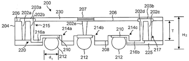
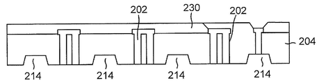
[0025]
도 2는 종래의 패시브-온-패키지(100)에 관하여 논의된 최소 두께(T)를 갖는 기판(204)을 포함하는 예시적인 패시브-온-패키지(200)를 도시한다. 예들 들어, 기판(204)이 유리를 포함하는 경우, 두께(T)는, 예를 들어, 적어도 100 마이크론일 수 있으므로, 기판(204)은 원하는 BLR(board level reliability)을 제공할 만큼 충분히 강인하다. 일반적으로, 최소 두께(T)는 기판(204)의 특성들에 의존한다. 예를 들어, 더 강인한 타입의 유리는 100 마이크론 초과까지 박형화될 수 있다. 반대로, 유리는 두께(T)가 150 마이크론 또는 그 이상이 되도록 덜 강인할 수 있다. 기판(204)이 실리콘과 같은 반도체 기판인 경우 두께(T)에 관한 유사한 제한들이 발생할 것이다. 대안으로, 기판(204)은 유기 기판을 포함할 수 있다. 회로 보드 또는 다른 패키지 기판에 대한 상호접속을 위한 솔더 볼들(212)과 같은 복수의 상호접속부들은 또한 종래의 패시브-온-패키지(100)에 관하여 논의된 동일한 최소 두께(d1)를 가질 수 있다. 솔더 볼(212)을 위한 최소 두께(d1)는 그의 구성에 따라 달라진다. 예를 들면, 솔더 볼들(212)이 무연 솔더를 포함하는 경우, 이들은 보다 취성이고, 따라서, 납을 함유하는 실시예와 비교하여, 보다 두꺼운 최소 두께(d1)를 필요로 할 것이다. 이러한 최소 치수들이 충족됨에도 불구하고, 패시브-온-패키지(200)는 패시브-온-패키지(100)의 높이(H1)에 비해 감소되는 높이(H2)를 갖는데, 기판(204)이 기판(204)의 제 1 면(208)에 형성된 대응하는 블라인드 비아들 또는 리세스들(214) 내에 솔더 볼들(212)을 수용하기 때문이다. 패시브-온-패키지(200)의 높이(H2)는 따라서, 대략 블라인드 비아들 또는 리세스들(214)의 깊이만큼 감소된다.[0025] FIG. 2 illustrates an exemplary passive-on-
[0026]
패시브-온-패키지(200)는 하나 또는 그 초과의 제 1 관통-기판 비아들, 이를 테면, 기판(204)의 제 1 표면(208)부터 기판(208)의 반대쪽 제 2 표면(206)까지 연장되는 제 1 관통-기판들(202a, 202b, 202c, 및 202d)을 포함한다. 먼저, 관통-기판 비아(202a)가 기판(204)의 제 2 표면(206) 상의 납 또는 도체(203a)를 통하여 제 1 관통-기판 비아(202a)에 결합하여, 임베딩된 인덕터(215)를 형성한다. 유사하게, 제 1 관통-기판 비아(202c)는 도체(203b)를 통해 제 1 관통-기판 비아(202d)에 결합하여 임베딩된 인덕터(217)를 형성한다. 각각의 임베딩된 인덕터(215 및 217)는, 기판(204)에 대한 두께(T)가 과도하게 얇지 않기 때문에, 유리하게도 강인한 인덕턴스를 갖는다. 예를 들어, 인덕터(215)가 둘러싸는 전류 루프 면적은 (다른 팩터들 중에서도) 각각의 제 1 관통-기판 비아(202a 및 202b)의 길이의 함수이다. 차례로, 제 1 관통-기판 비아 길이들은 기판(204)에 대한 두께(T)의 함수이다. 패시브-온-패키지(200)에 대한 유리하게 낮은 패키지 높이(H2)를 달성하기 위해서 두께(T)가 과도하게 감소될 필요가 없기 때문에, 제 1 관통-기판 비아들, 이를 테면, 비아들(202a 및 202b)이 인덕터(215)에 대한 향상된 인덕턴스를 제공하기 위해 상대적으로 길 수 있다.The passive-on-
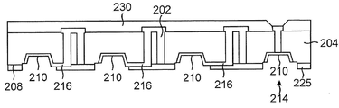
[0027]
인덕터들(215 및 217)에 결합시키는 것은 재배선 층(220)을 통해 발생할 수 있다. 예를 들어, 리세스(214a) 내에 수용되는 솔더 볼(212)이 재배선 층(220)으로부터 형성되는 재배선 층 도체(216a) 및 리세스 패드(210)를 통해 인덕터(215) 내의 제 1 관통-기판 비아(202b)에 결합한다. 다른 솔더 볼이 유사한 재배선 층 도체 및 패드(미도시)를 통해 제 1 관통-기판 비아(202a)에 결합하여 인덕터(215)에 대한 결합을 완료할 수 있다. 임베딩된 인덕터(217)에 관하여 유사한 결합이 제공될 수 있다. 예를 들면, 리세스(214c) 내에 수용되는 솔더 볼(212)은 재배선 층 도체(216b) 및 리세스 패드(210)를 통해 인덕터(217) 내의 제 1 관통-기판 비아(216b)에 결합된다. 일 실시예에서, 재배선 층(220)은, 리세스-수용 상호접속부들 중 특정한 상호접속부를 제 1 관통-기판 비아들 중 대응하는 비아들에 전기적으로 결합시키기 위한 수단을 포함하는 것으로 간주될 수 있다.[0027]
Coupling to
[0028]
제 1 관통-기판 비아들과는 대조적으로, 제 2 관통-기판 비아들은 감소된 길이를 가질 수 있다. 예를 들어, 제 2 관통-기판 비아(202e)는 리세스(214b)로부터 기판(204)의 제 2 표면(206)까지 연장된다. 실질적으로 기판(204)의 두께(T)와 동일한 제 1 관통-기판 비아들에 대한 길이에 비해, 제 2 관통-기판 비아(202e)는 리세스(214b)의 깊이 또는 높이만큼 짧아지는 길이를 갖는다. 이 감소된 길이는, 제 2 관통-기판 비아(202e)의 기판(204)의 표면(206) 상으로 통합되는 캐패시터(207)로의 결합 시 기생 인덕턴스 및 저항을 감소시킨다. 일 실시예에서, 캐패시터(207)는 MIM(metal-insulator-metal) 커패시터를 포함할 수 있다.[0028]
In contrast to the first through-substrate vias, the second through-substrate vias may have a reduced length. For example, a second through-via 202e extends from the
[0029]
리세스들(214)은 또한, 솔더 볼들(212)을 유지하는 데 도움이 되도록 접착제(미도시)를 포함할 수 있다. 제 1 및 제 2 관통-기판 비아들(202)은 전기 결합 기능뿐만 아니라 열 전달 역할 둘 모두를 제공할 수 있다. 제 2 관통-기판 비아들이, 제 1 관통-기판 비아들에 비해 이들의 감소된 길이로 인해 제 2 표면(206)으로부터, 대응하는 리세스들 내에 수용되는 솔더 볼들로의 열 전달에 특히 유용하다. 패시베이션 층 또는 솔더 레지스트 층(230)은 제 2 표면(206)을 커버할 수 있다. 유사하게, 패시베이션 층 또는 솔더 레지스트 층(225)은 기판(204)의 제 1 표면(208)을 커버할 수 있다. 패시베이션 층들(230 및 225)은 매우 다양한 적절한 재료들, 이를 테면, 실리콘 질화물, 폴리아미드(polymide)와 같은 유전성 중합체, 또는 유기 중합체들을 포함할 수 있다. [0029]
The
[0030]
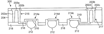
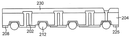
도 3a에 도시된 패시브-온-패키지(300)는 많은 대안적인 실시예들 중 하나를 포함한다. 이 실시예에서, 표면(206)은, 어떠한 관통-기판 비아들에 또는 다른 구조들에 결합하지 않는 솔더 볼(212)을 수용하는 리세스(214d)를 포함한다. 리세스(214d) 내의 솔더 볼(212)은 이와 같이, 전기 기능을 갖는 것과는 대조적으로, 패시브-온-패키지(300)를 대응하는 회로 보드 또는 추가 기판(미도시)에 기계적으로 결합시키는 기능만 한다. 패시브-온-패키지 기판(300) 내의 나머지 엘리먼트들은 패시브-온-패키지(200)에 관하여 논의된 바와 같다.[0030]
The passive-on-
[0031]
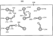
예시적인 패시브-온-패키지에 대한 기판(360)의 표면(208)의 평면도가, 제 1 관통-기판 비아들(202)에 대한 재배선 층 패드들(210) 및 재배선 층 도체들(216)에 대한 레이아웃을 더 잘 도시하기 위해 도 3b에 도시된다. 예시적인 리세스(214f)는, 재배선 층 도체(216)를 통해 제 1 관통 기판 비아(202)에 결합하는 재배선 층 패드(210)를 포함한다. 대조적으로, 리세스(214e)는 어떠한 재배선 층 도체에도 결합되지 않는 재배선 층 패드(210)를 포함한다. 리세스(214e) 내 패드(210)는 대신에 제 2 관통-기판 비아(미도시)에 결합될 수 있다. 대안으로, 리세스(214e)는, 도 3a의 리세스(214d)와 관련하여 논의된 바와 같이 기계 결합의 목적을 가질 뿐일 수 있다.[0031]
A top view of the
[0032]
도 2에 도시된 개시된 기판들, 이를 테면, 기판(204)에 대한 향상된 두께(T)는, 기판 두께가 감소되었을 경우 두께가 감소되지 않았다면 제조 동안 필요로 되었을, 일시적인 캐리어들의 제거를 가능하게 한다. 이외에도, 제 1 관통-기판 비아들(202)에 대한 길이가 증가될 수 있으며, 이는, 임베딩된 인덕터(215 및 217)와 같은 인덕터들에 대해 증가된 인덕턴스와 더 양호한 품질 팩터들에 이르게 한다. 이외에도, 기판(204)을 통한 더 나은 열 흐름은, 기판의 두께(T)에 비해 짧아지는 제 2 관통-기판 비아들, 이를 테면, 제 2 관통-기판 비아(202e)를 이용하여 달성될 수 있다. 이러한 비아(202e)의 동일한 단축은 또한 그의 저항을 감소시키며, 이는, 예를 들어, 캐패시터(207)에 대한 품질 팩터를 통해 구동되는 캐패시터들에 대한 품질 팩터를 증가시킨다. 이러한 제 2 관통-기판 비아들을 통과하는 결과적으로 감소된 신호 경로 길이는 또한 신호 통합의 향상에 유리하다. 이외에도, 리세스들(214)에서 수용되는 솔더 볼들(212)의 부분이 패키지 높이에 기여하지 않기 때문에, 솔더 볼들(212)은, BLR(board level reliability) 및 솔더 볼 크랙킹에 대한 저항을 또한 개선하는 최소 직경을 유지할 수 있다. 블라인드 비아들 또는 리세스들(214)은 또한 접착제의 사용을 수용하며, 이는 BLR을 추가로 개선한다. 마지막으로, 블라인드 비아들 또는 리세스들(214)은, 솔더 볼들(212)이 적은 오차로 대응하는 리세스들(214) 내에 수용될 수 있도록 제조 시 볼 적하 스테이지 동안 스텐실(stencil)로서 역할을 한다. 예시적인 제조 프로세스가 이제 논의될 것이다.[0032]
The improved thicknesses (T) for the disclosed substrates, such as
예시적인 제조 프로세스Exemplary manufacturing process
[0033] 다음의 설명은, 패시브-온-패키지의 패시브 컴포넌트들을 지지하기 위해 사용되는 기판이, 개별 패키지들로 다이싱되기 전에 웨이퍼 (또는 패널)의 부분으로서 프로세싱되는 웨이퍼-레벨-프로세스(WLP) 실시예들에 관한 것이다. 그러나, 본원에 논의되는 프로세스들은 또한, 웨이퍼(또는 패널)를 한 개로 프로세싱하는 것에 비해, 웨이퍼로부터 다이싱되었던 기판들에 개별적으로 적용될 수 있다는 것을 인식할 것이다. 감소된 높이를 달성하기 위해서 WLP 프로세스가 패시브-온-패키지들을 제조하기 위해 사용되는지 여부와 무관하게, 본원에 개시된 감소된 높이의 패시브-온-패키지들은 대응하는 블라인드 비아들 또는 리세스들 내에 솔더 볼들과 같은 상호접속부들을 수용한다.[0033] The following description is based on a wafer-level-process (WLP) embodiment in which the substrate used to support the passive components of the passive-on-package is processed as part of the wafer (or panel) Lt; / RTI > However, it will be appreciated that the processes discussed herein may also be applied separately to the substrates that have been diced from the wafer, as compared to processing the wafer (or panel) in one operation. The passive-on-packages of reduced height disclosed herein, regardless of whether the WLP process is used to fabricate passive-on-packages to achieve reduced heights, Such as balls.
[0034]
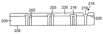
예시적인 제조 프로세스 흐름이 도 4a 내지 도 4e에 도시된다. 도 4a에 도시된 바와 같이, 유리 패널 또는 웨이퍼(또는 반도체 웨이퍼)와 같은 기판(204)은, 기판을 통과하는 비아들(202)을 형성하도록 프로세싱된다. 대안으로, 기판(204)은 라미네이트된 유기 패널을 포함할 수 있다. 관통-기판 비아들을 형성하기 위해서, 기판(204)은, 비아들을 형성하기 위해서 레이저 드릴, 기계 드릴, 또는 에칭 처리될 수 있고, 이 비아들은 이후 구리, 니켈, 또는 다른 적절한 금속들로 전기도금되어 관통-기판 비아들(202)을 형성한다. 대안으로, 무전해 프로세스가 전기도금 대신 사용될 수 있다. 관통-기판 비아 비아들(202)을 형성하기 위해 금속을 증착한 후, 기판(204)에 대한 제 1 표면(208) 및 반대쪽 제 2 표면(206)이 이후 폴리싱될 수 있다. 리세스들이 (보드-대향쪽 표면일 수 있는) 제 1 표면(208) 상에 아직 형성되지 않았기 때문에, 제 1 및 제 2 관통-기판 비아들 사이의 길이 차이가 아직 형성되지 않았다.[0034]
An exemplary manufacturing process flow is shown in Figures 4A-4E. As shown in FIG. 4A, a
[0035]
도 4b에 도시된 바와 같이, 기판(204)의 제 2 표면(206)은, 예를 들어, 대응하는 관통-기판 비아들을 연결하는 도체들(203)을 형성하여 인덕터들을 형성하기 위해서 포토리소그래픽 기술들을 통해, 패터닝된 금속 층, 이를 테면, 구리 또는 니켈 금속 층을 이용하여 프로세싱될 수 있다. 이외에도, 임의의 원하는 캐패시터들(미도시)을 형성하기 위한 표면(206) 상의 MIM 구조 증착이 또한 이 시점에서 수행될 수 있다. 또한, 패시베이션 층(230)이 이 제조 스테이지에서 표면(208) 위에 증착될 수 있다. 예를 들어, 다이로의 열 전달 또는 신호 전도를 위해 특정한 후속 관통-기판 비아들에 대해 컨택트가 필요로 될 경우, 도체들(203)을 형성하는 패터닝된 금속 층은 또한 패드들, 이를 테면, 패드(219)를 형성하기 위해 패터닝될 수 있다. 이러한 실시예에서, 패시베이션 층(230)은, 패드(219)를 노출시키기 위해서 패드 개구들, 이를 테면, 패드 개구(218)를 포함할 수 있다.[0035]
4b, the
[0036]
이후, 도 4c에 도시된 바와 같이, 표면(208)이 에칭되거나 또는 드릴링되어 블라인드 비아들 또는 리세스들(214)을 형성할 수 있다. 리세스들(214)의 에칭과 관련하여, 습식 또는 건식 에칭 기술들이 사용될 수 있다. 대안으로, 반응성 이온 에칭이 리세스들(214)을 에칭하기 위해 사용될 수 있다. 드릴링과 관련하여, 레이저 또는 기계식 드릴링 기술들이 적합하다. 도 4c의 단면도에서, 리세스들(214)이 임의의 관통-기판 비아들(202)과 교차하지 않으므로, 모든 이러한 도시된 비아들은 제 1 표면 비아들이다. 대안으로, 리세스가, 도 2의 리세스(214e)와 관련하여 앞서 설명된 바와 같은 관통-기판 비아와 교차하여, 제 2 관통-기판 비아(202e)(도 2에만 도시됨)를 형성할 수 있다.[0036]
The
[0037]
도 4d에 도시된 바와 같이, 재배선 층 패드들(210) 및 도체들(216)의 이면이 이후, 기판(204)의 표면(208) 상에 증착될 수 있다. 예를 들어, 마스크 층(미도시)이 이후 패드들(210) 및 도체들(216)을 형성하기 위해 구리, 니켈, 또는 다른 적합한 금속들의 도금을 위한 개구부들을 포함하도록 패터닝될 수 있다. 마지막으로, 솔더 볼들(214)은, 도 4f에 도시된 바와 같이, 리세스(214) 안으로 적하되고 리플로우된다. 이후, 기판(204)이 제조 프로세스를 완료하기 위해서 이때에 그의 패널 또는 웨이퍼(미도시)로부터 다이싱될 수 있다. 이제 제조 프로세스를 다음 흐름도에서 요약할 것이다.[0037]
The backside of the
예시적인 제조 프로세스 흐름도Exemplary Manufacturing Process Flow Diagram
[0038]
예시적인 제조 방법에 대한 흐름도가 도 5에 도시된다. 방법은, 기판의 제 1 표면 상에 제 1 리세스를 형성하는 단계(500)를 포함한다. 단계(505)는 기판을 통과하여 연장되는 복수의 제 1 관통-기판 비아들을 형성하는 단계를 포함한다. 도 2의 202d를 통과하는 비아들(202a)은 이러한 제 1 관통-기판 비아들의 예들이다. 단계(510)는 제 1 표면 상에 재배선 층을 형성하는 단계를 포함한다. 마지막으로, 단계(515)는 제 1 리세스 안으로 상호접속부를 결합시키는 단계를 포함하며, 재배선 층을 형성하는 단계는 제 1 관통-기판 비아들 중 대응하는 비아에 제 1 상호접속부를 결합시키는 도체를 형성한다. 예를 들어, 도 2의 재배선 층(220)을 형성하는 것은 도체(216a)를 리세스(214a) 내의 솔더 볼(212) 사이에서 제 1 관통-기판 비아(202b)에 결합시킨다. 이와 관련하여, 일부 리세스는, 이를 테면, 도 3a의 리세스(214d)가 임의의 재배선 층 도체들을 통해 임의의 관통-기판 비아들에 결합하지 않는 솔더 볼(212)을 수용한다는 것을 주목한다. 로우-프로파일 패시브-온-패키지를 유리하게 통합시킬 수 있는 일부 예시적인 전자 시스템들을 이제 논의할 것이다.[0038]
A flow chart for an exemplary manufacturing method is shown in FIG. The method includes forming (500) a first recess on a first surface of a substrate. Step 505 includes forming a plurality of first through-substrate vias extending through the substrate.
예시적이 전자 시스템들Exemplary electronic systems
[0039]
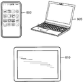
본원에 개시된 패시브-온-패키지가 매우 다양한 전자 시스템들에 포함될 수 있다. 예를 들어, 도 6에 도시된 바와 같이, 휴대 전화(600), 랩탑(605), 및 태블릿 PC(610)는 모두, 본 개시물에 따라 구성되는 로우-프로파일 패시브-온-패키지를 포함할 수 있다. 음악 플레이어, 비디오 플레이어, 통신 디바이스, 및 개인 컴퓨터와 같은 다른 예시적인 전자 시스템들은 또한 본 개시물에 따라 구성되는 패시브-온-패키지들로 구성될 수 있다. [0039]
The passive-on-package described herein can be incorporated into a wide variety of electronic systems. 6,
[0040] 이제 당업자가 인식하는 바와 같이 그리고 머지않아 쓸 수 있는 특정 용도에 의존하여, 본 개시물의 디바이스들의 재료들, 장치, 구성들 및 사용 방법들에 대하여 많은 변경들, 대체들 및 변형들이, 본 발명의 정신 및 범위로 부터 벗어나지 않고 이루어질 수 있다. 이러한 관점에서, 본 개시물의 범위는 본원에 예시되고 설명되는 특정 실시예들의 범위로 제한되지 않아야 하고, 이들은 단지 본 개시물의 일부 예시일 뿐이지만, 더 정확하게는, 이후에 첨부되는 청구항들 및 이들의 기능적 등가물들의 범위와 전적으로 상응되어야 한다.[0040] Many modifications, substitutions, and variations on the materials, apparatus, configurations, and methods of use of the devices of the present disclosure, as well as those skilled in the art will now recognize, and depending upon the particular use in which it may be used, Spirit and scope of the present invention. In view of this disclosure, the scope of the disclosure should not be limited to the specific embodiments illustrated and described herein, and they are merely some examples of the disclosure, but more precisely, Should fully correspond to the range of functional equivalents.
Claims (27)
기판;
상기 기판의 제 1 표면 상의 제 1 리세스;
상기 기판을 통과하여 연장되고 상기 기판의 두께와 실질적으로 동일한 길이를 갖는 복수의 제 1 관통-기판 비아들;
제 1 상호접속부 ―상기 제 1 상호접속부는 상기 제 1 리세스에 의해 수용됨―;
상기 기판의 상기 제 1 표면 상의 제 2 리세스;
상기 제 2 리세스로부터 상기 기판을 통과하여 연장되고 상기 제 2 리세스의 깊이만큼 짧아지는 기판의 두께와 실질적으로 동일한 길이를 갖는 제 2 관통-기판 비아;
상기 기판의 상기 제 1 표면 상의 재배선 층 ―상기 재배선 층은 상기 제 1 관통-기판 비아들 중 대응하는 비아에 상기 제 1 상호접속부를 전기적으로 결합시키도록 구성됨―; 및
상기 기판의 반대쪽 제 2 표면에 인접한 캐패시터를 포함하고,
상기 제 2 관통-기판 비아는 상기 캐패시터에 전기적으로 결합되는, 디바이스.As a device,
Board;
A first recess on a first surface of the substrate;
A plurality of first through-substrate vias extending through the substrate and having a length substantially equal to a thickness of the substrate;
A first interconnect, the first interconnect being received by the first recess;
A second recess on the first surface of the substrate;
A second through-substrate via extending from said second recess through said substrate and having a length substantially equal to a thickness of the substrate being shortened by a depth of said second recess;
A rewiring layer on the first surface of the substrate, the rewiring layer being configured to electrically couple the first interconnect to a corresponding one of the first penetrating-substrate vias; And
A capacitor adjacent the second surface opposite the substrate,
And wherein the second through-substrate via is electrically coupled to the capacitor.
임베딩된 인덕터를 더 포함하고,
상기 임베딩된 인덕터는 상기 제 1 관통-기판 비아들 중 적어도 2개를 포함하는, 디바이스.The method according to claim 1,
Further comprising an embedded inductor,
Wherein the embedded inductor comprises at least two of the first through-substrate vias.
상기 임베딩된 인덕터는 복수의 임베딩된 인덕터들을 포함하는, 디바이스.3. The method of claim 2,
Wherein the embedded inductor comprises a plurality of embedded inductors.
각각의 임베딩된 인덕터는, 상기 기판의 상기 반대쪽 제 2 표면에 인접한 도체를 통해 함께 전기적으로 결합되는 2개의 제 1 관통-기판 비아들을 포함하는, 디바이스.The method of claim 3,
Wherein each of the embedded inductors comprises two first through-substrate vias electrically coupled together through conductors adjacent the second opposing second surface of the substrate.
상기 기판은 유리 기판을 포함하고, 상기 제 1 상호접속부는 솔더 볼을 포함하는, 디바이스.The method according to claim 1,
Wherein the substrate comprises a glass substrate, and wherein the first interconnect comprises a solder ball.
상기 기판은 반도체 기판을 포함하고, 상기 제 1 상호접속부는 금속 기둥(pillar)을 포함하는, 디바이스.The method according to claim 1,
Wherein the substrate comprises a semiconductor substrate, and wherein the first interconnect comprises a metal pillar.
상기 기판은 유기 기판을 포함하고, 상기 제 1 상호접속부는 솔더 볼을 포함하는, 디바이스.The method according to claim 1,
Wherein the substrate comprises an organic substrate, and wherein the first interconnect comprises a solder ball.
상기 기판의 상기 제 1 표면 상의 제 3 리세스; 및
상기 제 3 리세스에 의해 수용되는 제 2 상호접속부를 더 포함하고,
상기 제 1 상호접속부 및 제 2 상호접속부는 대응하는 제 1 솔더 볼 및 제 2 솔더 볼을 포함하고, 상기 제 2 솔더 볼은 상기 디바이스를 회로 보드에 고정시키는 것에 대하여 기계적 기능만을 갖는, 디바이스.The method according to claim 1,
A third recess on the first surface of the substrate; And
Further comprising a second interconnect that is received by the third recess,
Wherein the first interconnect and the second interconnect comprise a corresponding first solder ball and a second solder ball and wherein the second solder ball has only mechanical function for securing the device to the circuit board.
기판의 제 1 표면 상에 제 1 리세스를 형성하는 단계;
상기 기판을 통과하여 연장되고 상기 기판의 두께와 실질적으로 동일한 길이를 갖는 복수의 제 1 관통-기판 비아들을 형성하는 단계;
상기 기판의 상기 제 1 표면 상에 제 2 리세스를 형성하는 단계;
상기 제 2 리세스로부터 상기 기판을 통과하여 연장되고 상기 제 2 리세스의 깊이만큼 짧아진 상기 기판의 두께와 실질적으로 동일한 길이를 갖는 제 2 관통-기판 비아를 형성하는 단계;
상기 기판의 상기 제 1 표면에 인접하게 재배선 층을 형성하는 단계;
상기 제 1 리세스 안으로 제 1 상호접속부를 결합시키는 단계 ―상기 재배선 층을 형성하는 단계는 상기 제 1 상호접속부를 상기 제 1 관통-기판 비아들 중 대응하는 비아에 결합시키는 도체를 형성함―; 및
상기 기판의 반대쪽 제 2 표면에 인접하게 캐패시터를 형성하는 단계를 포함하고,
상기 제 2 관통-기판 비아는 상기 캐패시터에 전기적으로 결합되는, 방법.As a method,
Forming a first recess on a first surface of the substrate;
Forming a plurality of first through-substrate vias extending through the substrate and having a length substantially equal to a thickness of the substrate;
Forming a second recess on the first surface of the substrate;
Forming a second through-via via extending from the second recess through the substrate and having a length substantially equal to a thickness of the substrate shortened by a depth of the second recess;
Forming a rewiring layer adjacent the first surface of the substrate;
Wherein the step of forming the rewiring layer comprises forming a conductor that couples the first interconnect to a corresponding one of the first through-substrate vias, ; And
Forming a capacitor adjacent the second surface opposite the substrate,
And wherein the second through-substrate via is electrically coupled to the capacitor.
상기 재배선 층을 형성하는 단계는 상기 제 1 표면 상에 금속층을 패터닝하는 단계를 포함하는, 방법.10. The method of claim 9,
Wherein the step of forming the rewiring layer comprises patterning a metal layer on the first surface.
상기 금속층을 패터닝하는 단계는 상기 제 1 리세스 내에 패드를 패터닝하는 단계를 더 포함하는, 방법.11. The method of claim 10,
Wherein patterning the metal layer further comprises patterning the pad in the first recess.
상기 금속층을 패터닝하는 단계는 구리 금속 층을 패터닝하는 단계를 포함하는, 방법.12. The method of claim 11,
Wherein patterning the metal layer comprises patterning a copper metal layer.
상기 제 2 리세스를 형성하는 단계는 복수의 제 2 리세스들을 형성하는 단계를 포함하고, 상기 제 2 관통-기판 비아를 형성하는 단계는 상기 복수의 제 2 리세스들에 대응하는 복수의 제 2 관통-기판 비아들을 형성하는 단계를 포함하고, 각각의 제 2 관통-기판 비아는 상기 대응하는 제 2 리세스로부터 상기 기판을 통과하여 연장되는, 방법.10. The method of claim 9,
Wherein forming the second recess comprises forming a plurality of second recesses, wherein forming the second through-via vias includes forming a plurality of second recesses corresponding to the plurality of second recesses, 2 through-substrate vias, each second through-substrate via extending from the corresponding second recess through the substrate.
상기 기판의 상기 제 1 표면 상에 그리고 상기 기판의 상기 반대쪽 제 2 표면 상에 패시베이션 층을 층착하는 단계를 더 포함하는, 방법.10. The method of claim 9,
Further comprising layering a passivation layer on the first surface of the substrate and on the second opposite surface of the substrate.
리세스들을 형성하는 단계는 유리 기판의 제 1 면을 에칭하는 단계를 포함하는, 방법.10. The method of claim 9,
Wherein forming the recesses comprises etching the first side of the glass substrate.
상기 제 1 상호접속부를 상기 제 1 리세스에 결합시키는 단계는 솔더 볼을 상기 제 1 리세스에 적하하는 단계를 포함하는, 방법.10. The method of claim 9,
Wherein coupling the first interconnect to the first recess comprises dipping solder balls into the first recess.
기판;
상기 기판을 통과하여 연장되고 상기 기판의 두께와 실질적으로 동일한 길이를 갖는 복수의 제 1 관통-기판 비아들;
한 쌍의 상기 복수의 제 1 관통-기판 비아들로부터 형성된 임베딩된 인덕터;
상기 기판의 제 1 표면 상의 제 1 리세스;
상기 기판의 상기 제 1 표면 상의 제 2 리세스;
상기 제 2 리세스로부터 상기 기판을 통과하여 연장되고 그리고 상기 제 2 리세스의 깊이만큼 짧아지는 상기 기판의 두께와 실질적으로 동일한 길이를 갖는 제 2 관통-기판 비아;
상기 제 1 리세스에 의해 수용되는 제 1 상호접속부;
상기 제 2 리세스에 의해 수용되는 제 2 상호접속부;
상기 제 1 상호접속부를 상기 임베딩된 인덕터에 전기적으로 결합시키기 위한 수단; 및
상기 기판의 반대쪽 제 2 표면에 인접한 캐패시터를 포함하고,
상기 제 2 관통 기판 비아는 상기 캐패시터를 상기 제 2 상호접속부에 전기적으로 결합시키는, 디바이스.As a device,
Board;
A plurality of first through-substrate vias extending through the substrate and having a length substantially equal to a thickness of the substrate;
An embedded inductor formed from a pair of said plurality of first through-substrate vias;
A first recess on a first surface of the substrate;
A second recess on the first surface of the substrate;
A second through-substrate via extending from said second recess through said substrate and having a length substantially equal to a thickness of said substrate that is shortened by a depth of said second recess;
A first interconnect that is received by the first recess;
A second interconnect that is received by the second recess;
Means for electrically coupling the first interconnect to the embedded inductor; And
A capacitor adjacent the second surface opposite the substrate,
And wherein the second through substrate via electrically couples the capacitor to the second interconnect.
상기 제 1 상호접속부 및 상기 제 2 상호접속부는 솔더 볼들을 포함하는, 디바이스.18. The method of claim 17,
Wherein the first interconnect and the second interconnect comprise solder balls.
상기 기판은 적어도 100 마이크론의 두께를 갖는 유리 기판을 포함하는, 디바이스.18. The method of claim 17,
Wherein the substrate comprises a glass substrate having a thickness of at least 100 microns.
유리 기판은 적어도 150 마이크론의 두께를 갖는, 디바이스.18. The method of claim 17,
Wherein the glass substrate has a thickness of at least 150 microns.
상기 수단은 적어도 하나의 패터닝된 금속 층을 포함하는, 디바이스.18. The method of claim 17,
Wherein the means comprises at least one patterned metal layer.
기판의 반대쪽 제 2 표면으로부터 기판 두께만큼 분리되는 제 1 면을 갖는 기판;
상기 기판의 상기 제 1 면 상의 복수의 리세스들;
상기 복수의 리세스들에 대응하는 복수의 솔더 볼들 ―각각의 솔더 볼은 솔더 볼 직경을 가지며 각각의 리세스는 상기 대응하는 솔더 볼을 수용하여, 상기 패키지에 대한 패키지 높이가 상기 기판 두께 및 상기 솔더 볼 직경의 합보다 작음―;
상기 제 1 면으로부터 연장되고, 상기 기판 두께와 실질적으로 동일한 길이를 각각 갖는 복수의 제 1 관통-기판 비아들
상기 복수의 리세스들 중 하나로부터 상기 기판을 관통하여 연장되고 그리고 제 2 리세스의 깊이만큼 짧아지는 상기 기판 두께와 실질적으로 동일한 길이를 갖는 제 2 관통-기판 비아;
상기 솔더 볼들 중 특정 솔더 볼들을 상기 제 1 관통-기판 비아들 중 대응하는 비아들에 전기적으로 결합시키도록 구성되는 재배선 층; 및
상기 기판의 상기 반대쪽 제 2 면에 인접한 캐패시터를 포함하고,
상기 제 2 관통-기판 비아는 상기 캐패시터에 전기적으로 결합되는, 패키지.As a package,
A substrate having a first side separated by a substrate thickness from an opposite second side of the substrate;
A plurality of recesses on the first surface of the substrate;
A plurality of solder balls corresponding to the plurality of recesses, each solder ball having a solder ball diameter, each recess receiving the corresponding solder ball, wherein a package height for the package is greater than a thickness of the substrate, Less than the sum of the solder ball diameters -;
A plurality of first through-substrate vias extending from the first surface and each having a length substantially equal to the substrate thickness,
A second through-substrate via extending through the substrate from one of the plurality of recesses and having a length substantially equal to the substrate thickness that is reduced by the depth of the second recess;
A rewiring layer configured to electrically couple specific ones of the solder balls to corresponding ones of the first through-via vias; And
And a capacitor adjacent the second opposite side of the substrate,
And wherein the second through-substrate via is electrically coupled to the capacitor.
상기 패키지는 셀폰, 랩탑, 태블릿, 음악 플레이어, 통신 디바이스, 컴퓨터, 및 비디오 플레이어 중 적어도 하나에 포함되는, 패키지.23. The method of claim 22,
Wherein the package is included in at least one of a cell phone, a laptop, a tablet, a music player, a communication device, a computer, and a video player.
상기 기판은 유리 기판인, 패키지.23. The method of claim 22,
Wherein the substrate is a glass substrate.
임베딩된 인덕터를 더 포함하고,
상기 임베딩된 인덕터는 한 쌍의 상기 제 1 관통-기판 비아들을 포함하는, 패키지.23. The method of claim 22,
Further comprising an embedded inductor,
Wherein the embedded inductor comprises a pair of the first through-substrate vias.
상기 기판은 반도체 기판인, 패키지.23. The method of claim 22,
Wherein the substrate is a semiconductor substrate.
상기 기판의 상기 제 1 표면 상의 제 3 리세스; 및
상기 제 3 리세스에 의해 수용되는 제 2 상호접속부를 더 포함하고,
상기 재배선 층은, 상기 제 1 상호접속부를 상기 인덕터를 형성하는 상기 제 1 관통-기판 비아들 중 적어도 2개 중 하나에 전기적으로 결합시키고 그리고 상기 제 2 상호접속부를 상기 인덕터를 형성하는 상기 제 1 관통-기판 비아들 중 적어도 2개 중 다른 하나에 전기적으로 결합시키도록 구성되는, 디바이스.3. The method of claim 2,
A third recess on the first surface of the substrate; And
Further comprising a second interconnect that is received by the third recess,
Wherein the rewiring layer electrically couples the first interconnect to one of the at least two of the first through-substrate vias forming the inductor and the second interconnect to the second interconnect- 1 < / RTI > through-substrate vias.
Applications Claiming Priority (5)
| Application Number | Priority Date | Filing Date | Title |
|---|---|---|---|
| US201461941308P | 2014-02-18 | 2014-02-18 | |
| US61/941,308 | 2014-02-18 | ||
| US14/200,684 US20150237732A1 (en) | 2014-02-18 | 2014-03-07 | Low-profile package with passive device |
| US14/200,684 | 2014-03-07 | ||
| PCT/US2015/014895 WO2015126640A1 (en) | 2014-02-18 | 2015-02-06 | Low-profile package with passive device |
Publications (1)
| Publication Number | Publication Date |
|---|---|
| KR20160123322A true KR20160123322A (en) | 2016-10-25 |
Family
ID=53799402
Family Applications (1)
| Application Number | Title | Priority Date | Filing Date |
|---|---|---|---|
| KR1020167024477A KR20160123322A (en) | 2014-02-18 | 2015-02-06 | Low-Profile Package with Passive Device |
Country Status (6)
| Country | Link |
|---|---|
| US (1) | US20150237732A1 (en) |
| EP (1) | EP3108502A1 (en) |
| JP (1) | JP2017515295A (en) |
| KR (1) | KR20160123322A (en) |
| CN (1) | CN106030782B (en) |
| WO (1) | WO2015126640A1 (en) |
Families Citing this family (12)
| Publication number | Priority date | Publication date | Assignee | Title |
|---|---|---|---|---|
| TWI607539B (en) * | 2015-02-16 | 2017-12-01 | 精材科技股份有限公司 | Chip package and manufacturing method thereof |
| US10321575B2 (en) | 2015-09-01 | 2019-06-11 | Qualcomm Incorporated | Integrated circuit (IC) module comprising an integrated circuit (IC) package and an interposer with embedded passive components |
| US10074625B2 (en) | 2015-09-20 | 2018-09-11 | Qualcomm Incorporated | Wafer level package (WLP) ball support using cavity structure |
| US20170092594A1 (en) * | 2015-09-25 | 2017-03-30 | Qualcomm Incorporated | Low profile package with passive device |
| US10044390B2 (en) | 2016-07-21 | 2018-08-07 | Qualcomm Incorporated | Glass substrate including passive-on-glass device and semiconductor die |
| US20180061775A1 (en) * | 2016-08-31 | 2018-03-01 | Qualcomm Incorporated | LOW PROFILE PASSIVE ON GLASS (PoG) DEVICE COMPRISING A DIE |
| DE102016116499B4 (en) * | 2016-09-02 | 2022-06-15 | Infineon Technologies Ag | Process for forming semiconductor devices and semiconductor devices |
| US10194529B2 (en) * | 2016-09-16 | 2019-01-29 | Qualcomm Incorporated | Partial metal fill for preventing extreme-low-k dielectric delamination |
| US10861840B2 (en) * | 2017-08-30 | 2020-12-08 | Advanced Semiconductor Engineering, Inc. | Integrated passive component and method for manufacturing the same |
| KR102513078B1 (en) * | 2018-10-12 | 2023-03-23 | 삼성전자주식회사 | Semiconductor package |
| CN110312363B (en) * | 2019-06-24 | 2020-10-16 | 维沃移动通信有限公司 | Printed circuit board assembly and terminal |
| CN111834341B (en) * | 2020-06-17 | 2021-09-21 | 珠海越亚半导体股份有限公司 | Capacitor and inductor embedded structure and manufacturing method thereof and substrate |
Family Cites Families (26)
| Publication number | Priority date | Publication date | Assignee | Title |
|---|---|---|---|---|
| US4074342A (en) * | 1974-12-20 | 1978-02-14 | International Business Machines Corporation | Electrical package for lsi devices and assembly process therefor |
| CA2034703A1 (en) * | 1990-01-23 | 1991-07-24 | Masanori Nishiguchi | Substrate for packaging a semiconductor device |
| JP2943788B2 (en) * | 1997-04-10 | 1999-08-30 | 日立エーアイシー株式会社 | Wiring board for mounting electronic components |
| JP2000068399A (en) * | 1998-08-19 | 2000-03-03 | Hitachi Denshi Ltd | Semiconductor device |
| US6569604B1 (en) * | 1999-06-30 | 2003-05-27 | International Business Machines Corporation | Blind via formation in a photoimageable dielectric material |
| JP4513222B2 (en) * | 2001-03-21 | 2010-07-28 | 富士通株式会社 | WIRING BOARD, MANUFACTURING METHOD THEREOF, AND SEMICONDUCTOR DEVICE USING THE SAME |
| US20030205799A1 (en) * | 2002-05-03 | 2003-11-06 | Mohammad Yunus | Method and device for assembly of ball grid array packages |
| US20040036170A1 (en) * | 2002-08-20 | 2004-02-26 | Lee Teck Kheng | Double bumping of flexible substrate for first and second level interconnects |
| JP2004207542A (en) * | 2002-12-26 | 2004-07-22 | Kyocera Corp | Package for storing light emitting element and light emitting device |
| JP4082220B2 (en) * | 2003-01-16 | 2008-04-30 | セイコーエプソン株式会社 | Wiring board, semiconductor module, and method of manufacturing semiconductor module |
| JP3926753B2 (en) * | 2003-03-06 | 2007-06-06 | 富士通株式会社 | Manufacturing method of connector board |
| US7327554B2 (en) * | 2003-03-19 | 2008-02-05 | Ngk Spark Plug Co., Ltd. | Assembly of semiconductor device, interposer and substrate |
| JP2004349457A (en) * | 2003-05-22 | 2004-12-09 | Matsushita Electric Ind Co Ltd | Large-scale integrated circuit (lsi) package |
| US7843302B2 (en) * | 2006-05-08 | 2010-11-30 | Ibiden Co., Ltd. | Inductor and electric power supply using it |
| US8084854B2 (en) * | 2007-12-28 | 2011-12-27 | Micron Technology, Inc. | Pass-through 3D interconnect for microelectronic dies and associated systems and methods |
| US20110050334A1 (en) * | 2009-09-02 | 2011-03-03 | Qualcomm Incorporated | Integrated Voltage Regulator with Embedded Passive Device(s) |
| US20130026609A1 (en) * | 2010-01-18 | 2013-01-31 | Marvell World Trade Ltd. | Package assembly including a semiconductor substrate with stress relief structure |
| US20110186960A1 (en) * | 2010-02-03 | 2011-08-04 | Albert Wu | Techniques and configurations for recessed semiconductor substrates |
| US8558392B2 (en) * | 2010-05-14 | 2013-10-15 | Stats Chippac, Ltd. | Semiconductor device and method of forming interconnect structure and mounting semiconductor die in recessed encapsulant |
| CN103119703B (en) * | 2010-09-23 | 2016-01-20 | 高通Mems科技公司 | Integrated passive device and power amplifier |
| US9579738B2 (en) * | 2011-02-25 | 2017-02-28 | International Business Machines Corporation | Flux composition and techniques for use thereof |
| US9058973B2 (en) * | 2011-04-13 | 2015-06-16 | International Business Machines Corporation | Passive devices fabricated on glass substrates, methods of manufacture and design structures |
| US9105627B2 (en) * | 2011-11-04 | 2015-08-11 | International Business Machines Corporation | Coil inductor for on-chip or on-chip stack |
| CN102723306B (en) * | 2012-06-28 | 2014-10-08 | 中国科学院上海微系统与信息技术研究所 | Microwave multi-chip packaging structure using silicon through hole and manufacture method thereof |
| US10312007B2 (en) * | 2012-12-11 | 2019-06-04 | Intel Corporation | Inductor formed in substrate |
| US9130016B2 (en) * | 2013-04-15 | 2015-09-08 | Schott Corporation | Method of manufacturing through-glass vias |
-
2014
- 2014-03-07 US US14/200,684 patent/US20150237732A1/en not_active Abandoned
-
2015
- 2015-02-06 CN CN201580008888.6A patent/CN106030782B/en active Active
- 2015-02-06 EP EP15706104.5A patent/EP3108502A1/en not_active Withdrawn
- 2015-02-06 JP JP2016552347A patent/JP2017515295A/en active Pending
- 2015-02-06 WO PCT/US2015/014895 patent/WO2015126640A1/en active Application Filing
- 2015-02-06 KR KR1020167024477A patent/KR20160123322A/en not_active Application Discontinuation
Also Published As
| Publication number | Publication date |
|---|---|
| US20150237732A1 (en) | 2015-08-20 |
| EP3108502A1 (en) | 2016-12-28 |
| JP2017515295A (en) | 2017-06-08 |
| WO2015126640A1 (en) | 2015-08-27 |
| CN106030782B (en) | 2020-01-14 |
| CN106030782A (en) | 2016-10-12 |
Similar Documents
| Publication | Publication Date | Title |
|---|---|---|
| KR20160123322A (en) | Low-Profile Package with Passive Device | |
| US8810008B2 (en) | Semiconductor element-embedded substrate, and method of manufacturing the substrate | |
| US9743530B2 (en) | Chip capacitors | |
| CN102820274B (en) | There is stress and reduce 3D integrated micro assembly of interconnection and preparation method thereof | |
| TWI508196B (en) | Method of making cavity substrate with built-in stiffener and cavity | |
| US6908785B2 (en) | Multi-chip package (MCP) with a conductive bar and method for manufacturing the same | |
| TWI689954B (en) | Polymer frame for chip with at least one through hole connected in series with capacitor | |
| KR20160015340A (en) | Bridge interconnection with layered interconnect structures | |
| JP2005327984A (en) | Electronic component and method of manufacturing electronic-component mounting structure | |
| JP2005209689A (en) | Semiconductor device and its manufacturing method | |
| KR20040107442A (en) | Semiconductor device and mounting structure thereof, and manufacturing method thereof | |
| KR20120000690A (en) | Semiconductor device and method of manufacturing the same | |
| KR102194722B1 (en) | Package board, method for manufacturing the same and package on package having the thereof | |
| US20180130745A1 (en) | Package substrate and its fabrication method | |
| JP2019149507A (en) | Semiconductor device and manufacturing method thereof | |
| WO2018182659A1 (en) | A die interconnect substrate, an electrical device and a method for forming a die interconnect substrate | |
| US20230262891A1 (en) | Connection structure embedded substrate and substrate structure including the same | |
| CN114334901A (en) | Semiconductor package structure and manufacturing method thereof | |
| TWI652864B (en) | Insert frame with polymer matrix and manufacturing method thereof | |
| CN111415921B (en) | Antenna packaging structure and manufacturing method thereof | |
| US11948899B2 (en) | Semiconductor substrate structure and manufacturing method thereof | |
| CN108428665B (en) | Integrated packaging process for laminated chip | |
| KR100986175B1 (en) | Semiconductor device and method for manufacturing the same | |
| CN113013112A (en) | Semiconductor structure and manufacturing method thereof | |
| KR20140114932A (en) | Package using a hybrid substrate and manufacturing method thereof |
Legal Events
| Date | Code | Title | Description |
|---|---|---|---|
| WITN | Application deemed withdrawn, e.g. because no request for examination was filed or no examination fee was paid |