JP2019149507A - Semiconductor device and manufacturing method thereof - Google Patents
Semiconductor device and manufacturing method thereof Download PDFInfo
- Publication number
- JP2019149507A JP2019149507A JP2018034557A JP2018034557A JP2019149507A JP 2019149507 A JP2019149507 A JP 2019149507A JP 2018034557 A JP2018034557 A JP 2018034557A JP 2018034557 A JP2018034557 A JP 2018034557A JP 2019149507 A JP2019149507 A JP 2019149507A
- Authority
- JP
- Japan
- Prior art keywords
- layer
- insulating layer
- semiconductor device
- wiring
- electrode layer
- Prior art date
- Legal status (The legal status is an assumption and is not a legal conclusion. Google has not performed a legal analysis and makes no representation as to the accuracy of the status listed.)
- Pending
Links
Images


Classifications
-
- H—ELECTRICITY
- H01—ELECTRIC ELEMENTS
- H01L—SEMICONDUCTOR DEVICES NOT COVERED BY CLASS H10
- H01L21/00—Processes or apparatus adapted for the manufacture or treatment of semiconductor or solid state devices or of parts thereof
- H01L21/02—Manufacture or treatment of semiconductor devices or of parts thereof
- H01L21/04—Manufacture or treatment of semiconductor devices or of parts thereof the devices having at least one potential-jump barrier or surface barrier, e.g. PN junction, depletion layer or carrier concentration layer
- H01L21/48—Manufacture or treatment of parts, e.g. containers, prior to assembly of the devices, using processes not provided for in a single one of the subgroups H01L21/06 - H01L21/326
- H01L21/4814—Conductive parts
- H01L21/4846—Leads on or in insulating or insulated substrates, e.g. metallisation
- H01L21/486—Via connections through the substrate with or without pins
-
- H—ELECTRICITY
- H01—ELECTRIC ELEMENTS
- H01L—SEMICONDUCTOR DEVICES NOT COVERED BY CLASS H10
- H01L21/00—Processes or apparatus adapted for the manufacture or treatment of semiconductor or solid state devices or of parts thereof
- H01L21/02—Manufacture or treatment of semiconductor devices or of parts thereof
- H01L21/04—Manufacture or treatment of semiconductor devices or of parts thereof the devices having at least one potential-jump barrier or surface barrier, e.g. PN junction, depletion layer or carrier concentration layer
- H01L21/50—Assembly of semiconductor devices using processes or apparatus not provided for in a single one of the subgroups H01L21/06 - H01L21/326, e.g. sealing of a cap to a base of a container
- H01L21/56—Encapsulations, e.g. encapsulation layers, coatings
- H01L21/561—Batch processing
-
- H—ELECTRICITY
- H01—ELECTRIC ELEMENTS
- H01L—SEMICONDUCTOR DEVICES NOT COVERED BY CLASS H10
- H01L21/00—Processes or apparatus adapted for the manufacture or treatment of semiconductor or solid state devices or of parts thereof
- H01L21/02—Manufacture or treatment of semiconductor devices or of parts thereof
- H01L21/04—Manufacture or treatment of semiconductor devices or of parts thereof the devices having at least one potential-jump barrier or surface barrier, e.g. PN junction, depletion layer or carrier concentration layer
- H01L21/50—Assembly of semiconductor devices using processes or apparatus not provided for in a single one of the subgroups H01L21/06 - H01L21/326, e.g. sealing of a cap to a base of a container
- H01L21/56—Encapsulations, e.g. encapsulation layers, coatings
- H01L21/565—Moulds
-
- H—ELECTRICITY
- H01—ELECTRIC ELEMENTS
- H01L—SEMICONDUCTOR DEVICES NOT COVERED BY CLASS H10
- H01L21/00—Processes or apparatus adapted for the manufacture or treatment of semiconductor or solid state devices or of parts thereof
- H01L21/02—Manufacture or treatment of semiconductor devices or of parts thereof
- H01L21/04—Manufacture or treatment of semiconductor devices or of parts thereof the devices having at least one potential-jump barrier or surface barrier, e.g. PN junction, depletion layer or carrier concentration layer
- H01L21/50—Assembly of semiconductor devices using processes or apparatus not provided for in a single one of the subgroups H01L21/06 - H01L21/326, e.g. sealing of a cap to a base of a container
- H01L21/56—Encapsulations, e.g. encapsulation layers, coatings
- H01L21/568—Temporary substrate used as encapsulation process aid
-
- H—ELECTRICITY
- H01—ELECTRIC ELEMENTS
- H01L—SEMICONDUCTOR DEVICES NOT COVERED BY CLASS H10
- H01L21/00—Processes or apparatus adapted for the manufacture or treatment of semiconductor or solid state devices or of parts thereof
- H01L21/67—Apparatus specially adapted for handling semiconductor or electric solid state devices during manufacture or treatment thereof; Apparatus specially adapted for handling wafers during manufacture or treatment of semiconductor or electric solid state devices or components ; Apparatus not specifically provided for elsewhere
- H01L21/683—Apparatus specially adapted for handling semiconductor or electric solid state devices during manufacture or treatment thereof; Apparatus specially adapted for handling wafers during manufacture or treatment of semiconductor or electric solid state devices or components ; Apparatus not specifically provided for elsewhere for supporting or gripping
- H01L21/6835—Apparatus specially adapted for handling semiconductor or electric solid state devices during manufacture or treatment thereof; Apparatus specially adapted for handling wafers during manufacture or treatment of semiconductor or electric solid state devices or components ; Apparatus not specifically provided for elsewhere for supporting or gripping using temporarily an auxiliary support
-
- H—ELECTRICITY
- H01—ELECTRIC ELEMENTS
- H01L—SEMICONDUCTOR DEVICES NOT COVERED BY CLASS H10
- H01L23/00—Details of semiconductor or other solid state devices
- H01L23/28—Encapsulations, e.g. encapsulating layers, coatings, e.g. for protection
- H01L23/31—Encapsulations, e.g. encapsulating layers, coatings, e.g. for protection characterised by the arrangement or shape
- H01L23/3107—Encapsulations, e.g. encapsulating layers, coatings, e.g. for protection characterised by the arrangement or shape the device being completely enclosed
- H01L23/3121—Encapsulations, e.g. encapsulating layers, coatings, e.g. for protection characterised by the arrangement or shape the device being completely enclosed a substrate forming part of the encapsulation
- H01L23/3128—Encapsulations, e.g. encapsulating layers, coatings, e.g. for protection characterised by the arrangement or shape the device being completely enclosed a substrate forming part of the encapsulation the substrate having spherical bumps for external connection
-
- H—ELECTRICITY
- H01—ELECTRIC ELEMENTS
- H01L—SEMICONDUCTOR DEVICES NOT COVERED BY CLASS H10
- H01L23/00—Details of semiconductor or other solid state devices
- H01L23/48—Arrangements for conducting electric current to or from the solid state body in operation, e.g. leads, terminal arrangements ; Selection of materials therefor
- H01L23/488—Arrangements for conducting electric current to or from the solid state body in operation, e.g. leads, terminal arrangements ; Selection of materials therefor consisting of soldered or bonded constructions
- H01L23/498—Leads, i.e. metallisations or lead-frames on insulating substrates, e.g. chip carriers
- H01L23/49811—Additional leads joined to the metallisation on the insulating substrate, e.g. pins, bumps, wires, flat leads
-
- H—ELECTRICITY
- H01—ELECTRIC ELEMENTS
- H01L—SEMICONDUCTOR DEVICES NOT COVERED BY CLASS H10
- H01L23/00—Details of semiconductor or other solid state devices
- H01L23/48—Arrangements for conducting electric current to or from the solid state body in operation, e.g. leads, terminal arrangements ; Selection of materials therefor
- H01L23/488—Arrangements for conducting electric current to or from the solid state body in operation, e.g. leads, terminal arrangements ; Selection of materials therefor consisting of soldered or bonded constructions
- H01L23/498—Leads, i.e. metallisations or lead-frames on insulating substrates, e.g. chip carriers
- H01L23/49827—Via connections through the substrates, e.g. pins going through the substrate, coaxial cables
-
- H—ELECTRICITY
- H01—ELECTRIC ELEMENTS
- H01L—SEMICONDUCTOR DEVICES NOT COVERED BY CLASS H10
- H01L23/00—Details of semiconductor or other solid state devices
- H01L23/48—Arrangements for conducting electric current to or from the solid state body in operation, e.g. leads, terminal arrangements ; Selection of materials therefor
- H01L23/488—Arrangements for conducting electric current to or from the solid state body in operation, e.g. leads, terminal arrangements ; Selection of materials therefor consisting of soldered or bonded constructions
- H01L23/498—Leads, i.e. metallisations or lead-frames on insulating substrates, e.g. chip carriers
- H01L23/49838—Geometry or layout
-
- H—ELECTRICITY
- H01—ELECTRIC ELEMENTS
- H01L—SEMICONDUCTOR DEVICES NOT COVERED BY CLASS H10
- H01L23/00—Details of semiconductor or other solid state devices
- H01L23/48—Arrangements for conducting electric current to or from the solid state body in operation, e.g. leads, terminal arrangements ; Selection of materials therefor
- H01L23/488—Arrangements for conducting electric current to or from the solid state body in operation, e.g. leads, terminal arrangements ; Selection of materials therefor consisting of soldered or bonded constructions
- H01L23/498—Leads, i.e. metallisations or lead-frames on insulating substrates, e.g. chip carriers
- H01L23/49866—Leads, i.e. metallisations or lead-frames on insulating substrates, e.g. chip carriers characterised by the materials
-
- H—ELECTRICITY
- H01—ELECTRIC ELEMENTS
- H01L—SEMICONDUCTOR DEVICES NOT COVERED BY CLASS H10
- H01L24/00—Arrangements for connecting or disconnecting semiconductor or solid-state bodies; Methods or apparatus related thereto
- H01L24/01—Means for bonding being attached to, or being formed on, the surface to be connected, e.g. chip-to-package, die-attach, "first-level" interconnects; Manufacturing methods related thereto
- H01L24/10—Bump connectors ; Manufacturing methods related thereto
- H01L24/12—Structure, shape, material or disposition of the bump connectors prior to the connecting process
- H01L24/14—Structure, shape, material or disposition of the bump connectors prior to the connecting process of a plurality of bump connectors
-
- H—ELECTRICITY
- H01—ELECTRIC ELEMENTS
- H01L—SEMICONDUCTOR DEVICES NOT COVERED BY CLASS H10
- H01L24/00—Arrangements for connecting or disconnecting semiconductor or solid-state bodies; Methods or apparatus related thereto
- H01L24/93—Batch processes
- H01L24/95—Batch processes at chip-level, i.e. with connecting carried out on a plurality of singulated devices, i.e. on diced chips
- H01L24/97—Batch processes at chip-level, i.e. with connecting carried out on a plurality of singulated devices, i.e. on diced chips the devices being connected to a common substrate, e.g. interposer, said common substrate being separable into individual assemblies after connecting
-
- H—ELECTRICITY
- H01—ELECTRIC ELEMENTS
- H01L—SEMICONDUCTOR DEVICES NOT COVERED BY CLASS H10
- H01L25/00—Assemblies consisting of a plurality of individual semiconductor or other solid state devices ; Multistep manufacturing processes thereof
- H01L25/03—Assemblies consisting of a plurality of individual semiconductor or other solid state devices ; Multistep manufacturing processes thereof all the devices being of a type provided for in the same subgroup of groups H01L27/00 - H01L33/00, or in a single subclass of H10K, H10N, e.g. assemblies of rectifier diodes
- H01L25/04—Assemblies consisting of a plurality of individual semiconductor or other solid state devices ; Multistep manufacturing processes thereof all the devices being of a type provided for in the same subgroup of groups H01L27/00 - H01L33/00, or in a single subclass of H10K, H10N, e.g. assemblies of rectifier diodes the devices not having separate containers
- H01L25/065—Assemblies consisting of a plurality of individual semiconductor or other solid state devices ; Multistep manufacturing processes thereof all the devices being of a type provided for in the same subgroup of groups H01L27/00 - H01L33/00, or in a single subclass of H10K, H10N, e.g. assemblies of rectifier diodes the devices not having separate containers the devices being of a type provided for in group H01L27/00
- H01L25/0657—Stacked arrangements of devices
-
- H—ELECTRICITY
- H01—ELECTRIC ELEMENTS
- H01L—SEMICONDUCTOR DEVICES NOT COVERED BY CLASS H10
- H01L25/00—Assemblies consisting of a plurality of individual semiconductor or other solid state devices ; Multistep manufacturing processes thereof
- H01L25/50—Multistep manufacturing processes of assemblies consisting of devices, each device being of a type provided for in group H01L27/00 or H01L29/00
-
- H—ELECTRICITY
- H01—ELECTRIC ELEMENTS
- H01L—SEMICONDUCTOR DEVICES NOT COVERED BY CLASS H10
- H01L2221/00—Processes or apparatus adapted for the manufacture or treatment of semiconductor or solid state devices or of parts thereof covered by H01L21/00
- H01L2221/67—Apparatus for handling semiconductor or electric solid state devices during manufacture or treatment thereof; Apparatus for handling wafers during manufacture or treatment of semiconductor or electric solid state devices or components; Apparatus not specifically provided for elsewhere
- H01L2221/683—Apparatus for handling semiconductor or electric solid state devices during manufacture or treatment thereof; Apparatus for handling wafers during manufacture or treatment of semiconductor or electric solid state devices or components; Apparatus not specifically provided for elsewhere for supporting or gripping
- H01L2221/68304—Apparatus for handling semiconductor or electric solid state devices during manufacture or treatment thereof; Apparatus for handling wafers during manufacture or treatment of semiconductor or electric solid state devices or components; Apparatus not specifically provided for elsewhere for supporting or gripping using temporarily an auxiliary support
- H01L2221/68345—Apparatus for handling semiconductor or electric solid state devices during manufacture or treatment thereof; Apparatus for handling wafers during manufacture or treatment of semiconductor or electric solid state devices or components; Apparatus not specifically provided for elsewhere for supporting or gripping using temporarily an auxiliary support used as a support during the manufacture of self supporting substrates
-
- H—ELECTRICITY
- H01—ELECTRIC ELEMENTS
- H01L—SEMICONDUCTOR DEVICES NOT COVERED BY CLASS H10
- H01L2224/00—Indexing scheme for arrangements for connecting or disconnecting semiconductor or solid-state bodies and methods related thereto as covered by H01L24/00
- H01L2224/01—Means for bonding being attached to, or being formed on, the surface to be connected, e.g. chip-to-package, die-attach, "first-level" interconnects; Manufacturing methods related thereto
- H01L2224/10—Bump connectors; Manufacturing methods related thereto
- H01L2224/15—Structure, shape, material or disposition of the bump connectors after the connecting process
- H01L2224/16—Structure, shape, material or disposition of the bump connectors after the connecting process of an individual bump connector
- H01L2224/161—Disposition
- H01L2224/16135—Disposition the bump connector connecting between different semiconductor or solid-state bodies, i.e. chip-to-chip
- H01L2224/16145—Disposition the bump connector connecting between different semiconductor or solid-state bodies, i.e. chip-to-chip the bodies being stacked
-
- H—ELECTRICITY
- H01—ELECTRIC ELEMENTS
- H01L—SEMICONDUCTOR DEVICES NOT COVERED BY CLASS H10
- H01L2224/00—Indexing scheme for arrangements for connecting or disconnecting semiconductor or solid-state bodies and methods related thereto as covered by H01L24/00
- H01L2224/01—Means for bonding being attached to, or being formed on, the surface to be connected, e.g. chip-to-package, die-attach, "first-level" interconnects; Manufacturing methods related thereto
- H01L2224/10—Bump connectors; Manufacturing methods related thereto
- H01L2224/15—Structure, shape, material or disposition of the bump connectors after the connecting process
- H01L2224/16—Structure, shape, material or disposition of the bump connectors after the connecting process of an individual bump connector
- H01L2224/161—Disposition
- H01L2224/16151—Disposition the bump connector connecting between a semiconductor or solid-state body and an item not being a semiconductor or solid-state body, e.g. chip-to-substrate, chip-to-passive
- H01L2224/16221—Disposition the bump connector connecting between a semiconductor or solid-state body and an item not being a semiconductor or solid-state body, e.g. chip-to-substrate, chip-to-passive the body and the item being stacked
- H01L2224/16225—Disposition the bump connector connecting between a semiconductor or solid-state body and an item not being a semiconductor or solid-state body, e.g. chip-to-substrate, chip-to-passive the body and the item being stacked the item being non-metallic, e.g. insulating substrate with or without metallisation
- H01L2224/16235—Disposition the bump connector connecting between a semiconductor or solid-state body and an item not being a semiconductor or solid-state body, e.g. chip-to-substrate, chip-to-passive the body and the item being stacked the item being non-metallic, e.g. insulating substrate with or without metallisation the bump connector connecting to a via metallisation of the item
-
- H—ELECTRICITY
- H01—ELECTRIC ELEMENTS
- H01L—SEMICONDUCTOR DEVICES NOT COVERED BY CLASS H10
- H01L2224/00—Indexing scheme for arrangements for connecting or disconnecting semiconductor or solid-state bodies and methods related thereto as covered by H01L24/00
- H01L2224/01—Means for bonding being attached to, or being formed on, the surface to be connected, e.g. chip-to-package, die-attach, "first-level" interconnects; Manufacturing methods related thereto
- H01L2224/26—Layer connectors, e.g. plate connectors, solder or adhesive layers; Manufacturing methods related thereto
- H01L2224/28—Structure, shape, material or disposition of the layer connectors prior to the connecting process
- H01L2224/29—Structure, shape, material or disposition of the layer connectors prior to the connecting process of an individual layer connector
- H01L2224/29001—Core members of the layer connector
- H01L2224/29099—Material
- H01L2224/2919—Material with a principal constituent of the material being a polymer, e.g. polyester, phenolic based polymer, epoxy
-
- H—ELECTRICITY
- H01—ELECTRIC ELEMENTS
- H01L—SEMICONDUCTOR DEVICES NOT COVERED BY CLASS H10
- H01L2224/00—Indexing scheme for arrangements for connecting or disconnecting semiconductor or solid-state bodies and methods related thereto as covered by H01L24/00
- H01L2224/01—Means for bonding being attached to, or being formed on, the surface to be connected, e.g. chip-to-package, die-attach, "first-level" interconnects; Manufacturing methods related thereto
- H01L2224/26—Layer connectors, e.g. plate connectors, solder or adhesive layers; Manufacturing methods related thereto
- H01L2224/31—Structure, shape, material or disposition of the layer connectors after the connecting process
- H01L2224/32—Structure, shape, material or disposition of the layer connectors after the connecting process of an individual layer connector
- H01L2224/321—Disposition
- H01L2224/32151—Disposition the layer connector connecting between a semiconductor or solid-state body and an item not being a semiconductor or solid-state body, e.g. chip-to-substrate, chip-to-passive
- H01L2224/32221—Disposition the layer connector connecting between a semiconductor or solid-state body and an item not being a semiconductor or solid-state body, e.g. chip-to-substrate, chip-to-passive the body and the item being stacked
- H01L2224/32225—Disposition the layer connector connecting between a semiconductor or solid-state body and an item not being a semiconductor or solid-state body, e.g. chip-to-substrate, chip-to-passive the body and the item being stacked the item being non-metallic, e.g. insulating substrate with or without metallisation
-
- H—ELECTRICITY
- H01—ELECTRIC ELEMENTS
- H01L—SEMICONDUCTOR DEVICES NOT COVERED BY CLASS H10
- H01L2224/00—Indexing scheme for arrangements for connecting or disconnecting semiconductor or solid-state bodies and methods related thereto as covered by H01L24/00
- H01L2224/73—Means for bonding being of different types provided for in two or more of groups H01L2224/10, H01L2224/18, H01L2224/26, H01L2224/34, H01L2224/42, H01L2224/50, H01L2224/63, H01L2224/71
- H01L2224/732—Location after the connecting process
- H01L2224/73201—Location after the connecting process on the same surface
- H01L2224/73203—Bump and layer connectors
- H01L2224/73204—Bump and layer connectors the bump connector being embedded into the layer connector
-
- H—ELECTRICITY
- H01—ELECTRIC ELEMENTS
- H01L—SEMICONDUCTOR DEVICES NOT COVERED BY CLASS H10
- H01L2224/00—Indexing scheme for arrangements for connecting or disconnecting semiconductor or solid-state bodies and methods related thereto as covered by H01L24/00
- H01L2224/80—Methods for connecting semiconductor or other solid state bodies using means for bonding being attached to, or being formed on, the surface to be connected
- H01L2224/81—Methods for connecting semiconductor or other solid state bodies using means for bonding being attached to, or being formed on, the surface to be connected using a bump connector
- H01L2224/81001—Methods for connecting semiconductor or other solid state bodies using means for bonding being attached to, or being formed on, the surface to be connected using a bump connector involving a temporary auxiliary member not forming part of the bonding apparatus
-
- H—ELECTRICITY
- H01—ELECTRIC ELEMENTS
- H01L—SEMICONDUCTOR DEVICES NOT COVERED BY CLASS H10
- H01L2224/00—Indexing scheme for arrangements for connecting or disconnecting semiconductor or solid-state bodies and methods related thereto as covered by H01L24/00
- H01L2224/91—Methods for connecting semiconductor or solid state bodies including different methods provided for in two or more of groups H01L2224/80 - H01L2224/90
- H01L2224/92—Specific sequence of method steps
- H01L2224/921—Connecting a surface with connectors of different types
- H01L2224/9212—Sequential connecting processes
- H01L2224/92122—Sequential connecting processes the first connecting process involving a bump connector
- H01L2224/92125—Sequential connecting processes the first connecting process involving a bump connector the second connecting process involving a layer connector
-
- H—ELECTRICITY
- H01—ELECTRIC ELEMENTS
- H01L—SEMICONDUCTOR DEVICES NOT COVERED BY CLASS H10
- H01L2225/00—Details relating to assemblies covered by the group H01L25/00 but not provided for in its subgroups
- H01L2225/03—All the devices being of a type provided for in the same subgroup of groups H01L27/00 - H01L33/648 and H10K99/00
- H01L2225/04—All the devices being of a type provided for in the same subgroup of groups H01L27/00 - H01L33/648 and H10K99/00 the devices not having separate containers
- H01L2225/065—All the devices being of a type provided for in the same subgroup of groups H01L27/00 - H01L33/648 and H10K99/00 the devices not having separate containers the devices being of a type provided for in group H01L27/00
- H01L2225/06503—Stacked arrangements of devices
- H01L2225/06513—Bump or bump-like direct electrical connections between devices, e.g. flip-chip connection, solder bumps
-
- H—ELECTRICITY
- H01—ELECTRIC ELEMENTS
- H01L—SEMICONDUCTOR DEVICES NOT COVERED BY CLASS H10
- H01L2225/00—Details relating to assemblies covered by the group H01L25/00 but not provided for in its subgroups
- H01L2225/03—All the devices being of a type provided for in the same subgroup of groups H01L27/00 - H01L33/648 and H10K99/00
- H01L2225/04—All the devices being of a type provided for in the same subgroup of groups H01L27/00 - H01L33/648 and H10K99/00 the devices not having separate containers
- H01L2225/065—All the devices being of a type provided for in the same subgroup of groups H01L27/00 - H01L33/648 and H10K99/00 the devices not having separate containers the devices being of a type provided for in group H01L27/00
- H01L2225/06503—Stacked arrangements of devices
- H01L2225/06517—Bump or bump-like direct electrical connections from device to substrate
-
- H—ELECTRICITY
- H01—ELECTRIC ELEMENTS
- H01L—SEMICONDUCTOR DEVICES NOT COVERED BY CLASS H10
- H01L2225/00—Details relating to assemblies covered by the group H01L25/00 but not provided for in its subgroups
- H01L2225/03—All the devices being of a type provided for in the same subgroup of groups H01L27/00 - H01L33/648 and H10K99/00
- H01L2225/04—All the devices being of a type provided for in the same subgroup of groups H01L27/00 - H01L33/648 and H10K99/00 the devices not having separate containers
- H01L2225/065—All the devices being of a type provided for in the same subgroup of groups H01L27/00 - H01L33/648 and H10K99/00 the devices not having separate containers the devices being of a type provided for in group H01L27/00
- H01L2225/06503—Stacked arrangements of devices
- H01L2225/06548—Conductive via connections through the substrate, container, or encapsulation
-
- H—ELECTRICITY
- H01—ELECTRIC ELEMENTS
- H01L—SEMICONDUCTOR DEVICES NOT COVERED BY CLASS H10
- H01L2225/00—Details relating to assemblies covered by the group H01L25/00 but not provided for in its subgroups
- H01L2225/03—All the devices being of a type provided for in the same subgroup of groups H01L27/00 - H01L33/648 and H10K99/00
- H01L2225/04—All the devices being of a type provided for in the same subgroup of groups H01L27/00 - H01L33/648 and H10K99/00 the devices not having separate containers
- H01L2225/065—All the devices being of a type provided for in the same subgroup of groups H01L27/00 - H01L33/648 and H10K99/00 the devices not having separate containers the devices being of a type provided for in group H01L27/00
- H01L2225/06503—Stacked arrangements of devices
- H01L2225/06555—Geometry of the stack, e.g. form of the devices, geometry to facilitate stacking
- H01L2225/06565—Geometry of the stack, e.g. form of the devices, geometry to facilitate stacking the devices having the same size and there being no auxiliary carrier between the devices
-
- H—ELECTRICITY
- H01—ELECTRIC ELEMENTS
- H01L—SEMICONDUCTOR DEVICES NOT COVERED BY CLASS H10
- H01L2225/00—Details relating to assemblies covered by the group H01L25/00 but not provided for in its subgroups
- H01L2225/03—All the devices being of a type provided for in the same subgroup of groups H01L27/00 - H01L33/648 and H10K99/00
- H01L2225/04—All the devices being of a type provided for in the same subgroup of groups H01L27/00 - H01L33/648 and H10K99/00 the devices not having separate containers
- H01L2225/065—All the devices being of a type provided for in the same subgroup of groups H01L27/00 - H01L33/648 and H10K99/00 the devices not having separate containers the devices being of a type provided for in group H01L27/00
- H01L2225/06503—Stacked arrangements of devices
- H01L2225/06582—Housing for the assembly, e.g. chip scale package [CSP]
- H01L2225/06586—Housing with external bump or bump-like connectors
-
- H—ELECTRICITY
- H01—ELECTRIC ELEMENTS
- H01L—SEMICONDUCTOR DEVICES NOT COVERED BY CLASS H10
- H01L23/00—Details of semiconductor or other solid state devices
- H01L23/48—Arrangements for conducting electric current to or from the solid state body in operation, e.g. leads, terminal arrangements ; Selection of materials therefor
- H01L23/488—Arrangements for conducting electric current to or from the solid state body in operation, e.g. leads, terminal arrangements ; Selection of materials therefor consisting of soldered or bonded constructions
- H01L23/498—Leads, i.e. metallisations or lead-frames on insulating substrates, e.g. chip carriers
- H01L23/49811—Additional leads joined to the metallisation on the insulating substrate, e.g. pins, bumps, wires, flat leads
- H01L23/49816—Spherical bumps on the substrate for external connection, e.g. ball grid arrays [BGA]
-
- H—ELECTRICITY
- H01—ELECTRIC ELEMENTS
- H01L—SEMICONDUCTOR DEVICES NOT COVERED BY CLASS H10
- H01L23/00—Details of semiconductor or other solid state devices
- H01L23/48—Arrangements for conducting electric current to or from the solid state body in operation, e.g. leads, terminal arrangements ; Selection of materials therefor
- H01L23/488—Arrangements for conducting electric current to or from the solid state body in operation, e.g. leads, terminal arrangements ; Selection of materials therefor consisting of soldered or bonded constructions
- H01L23/498—Leads, i.e. metallisations or lead-frames on insulating substrates, e.g. chip carriers
- H01L23/49822—Multilayer substrates
-
- H—ELECTRICITY
- H01—ELECTRIC ELEMENTS
- H01L—SEMICONDUCTOR DEVICES NOT COVERED BY CLASS H10
- H01L24/00—Arrangements for connecting or disconnecting semiconductor or solid-state bodies; Methods or apparatus related thereto
- H01L24/01—Means for bonding being attached to, or being formed on, the surface to be connected, e.g. chip-to-package, die-attach, "first-level" interconnects; Manufacturing methods related thereto
- H01L24/10—Bump connectors ; Manufacturing methods related thereto
- H01L24/15—Structure, shape, material or disposition of the bump connectors after the connecting process
- H01L24/16—Structure, shape, material or disposition of the bump connectors after the connecting process of an individual bump connector
-
- H—ELECTRICITY
- H01—ELECTRIC ELEMENTS
- H01L—SEMICONDUCTOR DEVICES NOT COVERED BY CLASS H10
- H01L24/00—Arrangements for connecting or disconnecting semiconductor or solid-state bodies; Methods or apparatus related thereto
- H01L24/01—Means for bonding being attached to, or being formed on, the surface to be connected, e.g. chip-to-package, die-attach, "first-level" interconnects; Manufacturing methods related thereto
- H01L24/26—Layer connectors, e.g. plate connectors, solder or adhesive layers; Manufacturing methods related thereto
- H01L24/28—Structure, shape, material or disposition of the layer connectors prior to the connecting process
- H01L24/29—Structure, shape, material or disposition of the layer connectors prior to the connecting process of an individual layer connector
-
- H—ELECTRICITY
- H01—ELECTRIC ELEMENTS
- H01L—SEMICONDUCTOR DEVICES NOT COVERED BY CLASS H10
- H01L24/00—Arrangements for connecting or disconnecting semiconductor or solid-state bodies; Methods or apparatus related thereto
- H01L24/01—Means for bonding being attached to, or being formed on, the surface to be connected, e.g. chip-to-package, die-attach, "first-level" interconnects; Manufacturing methods related thereto
- H01L24/26—Layer connectors, e.g. plate connectors, solder or adhesive layers; Manufacturing methods related thereto
- H01L24/31—Structure, shape, material or disposition of the layer connectors after the connecting process
- H01L24/32—Structure, shape, material or disposition of the layer connectors after the connecting process of an individual layer connector
-
- H—ELECTRICITY
- H01—ELECTRIC ELEMENTS
- H01L—SEMICONDUCTOR DEVICES NOT COVERED BY CLASS H10
- H01L24/00—Arrangements for connecting or disconnecting semiconductor or solid-state bodies; Methods or apparatus related thereto
- H01L24/73—Means for bonding being of different types provided for in two or more of groups H01L24/10, H01L24/18, H01L24/26, H01L24/34, H01L24/42, H01L24/50, H01L24/63, H01L24/71
-
- H—ELECTRICITY
- H01—ELECTRIC ELEMENTS
- H01L—SEMICONDUCTOR DEVICES NOT COVERED BY CLASS H10
- H01L24/00—Arrangements for connecting or disconnecting semiconductor or solid-state bodies; Methods or apparatus related thereto
- H01L24/80—Methods for connecting semiconductor or other solid state bodies using means for bonding being attached to, or being formed on, the surface to be connected
- H01L24/81—Methods for connecting semiconductor or other solid state bodies using means for bonding being attached to, or being formed on, the surface to be connected using a bump connector
-
- H—ELECTRICITY
- H01—ELECTRIC ELEMENTS
- H01L—SEMICONDUCTOR DEVICES NOT COVERED BY CLASS H10
- H01L24/00—Arrangements for connecting or disconnecting semiconductor or solid-state bodies; Methods or apparatus related thereto
- H01L24/91—Methods for connecting semiconductor or solid state bodies including different methods provided for in two or more of groups H01L24/80 - H01L24/90
- H01L24/92—Specific sequence of method steps
-
- H—ELECTRICITY
- H01—ELECTRIC ELEMENTS
- H01L—SEMICONDUCTOR DEVICES NOT COVERED BY CLASS H10
- H01L2924/00—Indexing scheme for arrangements or methods for connecting or disconnecting semiconductor or solid-state bodies as covered by H01L24/00
- H01L2924/0001—Technical content checked by a classifier
- H01L2924/00014—Technical content checked by a classifier the subject-matter covered by the group, the symbol of which is combined with the symbol of this group, being disclosed without further technical details
-
- H—ELECTRICITY
- H01—ELECTRIC ELEMENTS
- H01L—SEMICONDUCTOR DEVICES NOT COVERED BY CLASS H10
- H01L2924/00—Indexing scheme for arrangements or methods for connecting or disconnecting semiconductor or solid-state bodies as covered by H01L24/00
- H01L2924/15—Details of package parts other than the semiconductor or other solid state devices to be connected
- H01L2924/151—Die mounting substrate
- H01L2924/153—Connection portion
- H01L2924/1531—Connection portion the connection portion being formed only on the surface of the substrate opposite to the die mounting surface
- H01L2924/15311—Connection portion the connection portion being formed only on the surface of the substrate opposite to the die mounting surface being a ball array, e.g. BGA
-
- H—ELECTRICITY
- H01—ELECTRIC ELEMENTS
- H01L—SEMICONDUCTOR DEVICES NOT COVERED BY CLASS H10
- H01L2924/00—Indexing scheme for arrangements or methods for connecting or disconnecting semiconductor or solid-state bodies as covered by H01L24/00
- H01L2924/15—Details of package parts other than the semiconductor or other solid state devices to be connected
- H01L2924/151—Die mounting substrate
- H01L2924/153—Connection portion
- H01L2924/1532—Connection portion the connection portion being formed on the die mounting surface of the substrate
- H01L2924/15321—Connection portion the connection portion being formed on the die mounting surface of the substrate being a ball array, e.g. BGA
Abstract
Description
実施形態は、半導体装置及びその製造方法に関する。 Embodiments described herein relate generally to a semiconductor device and a manufacturing method thereof.
従来より、プリント基板上にメモリチップを複数枚積層し、樹脂でモールドした半導体装置が製造されている。プリント基板の下面にはバンプが接合されており、このバンプを介して、半導体装置が電子機器等に実装される。一方、近年、半導体装置の低背化が要求されているため、プリント基板の替わりに再配線層を用いる技術が提案されている。再配線層は支持基板上に半導体プロセスによって形成され、再配線層上にチップが積層された後、支持基板が除去される。再配線層の下面上には電極層が設けられ、この電極層にバンプが接合される。しかしながら、支持基板が除去された後の再配線層には反りが生じやすく、電極層を精度よく形成することが困難である。 Conventionally, a semiconductor device in which a plurality of memory chips are stacked on a printed circuit board and molded with a resin has been manufactured. Bumps are bonded to the lower surface of the printed circuit board, and the semiconductor device is mounted on an electronic device or the like via the bumps. On the other hand, in recent years, since a reduction in the height of a semiconductor device has been demanded, a technique using a rewiring layer instead of a printed circuit board has been proposed. The rewiring layer is formed on the support substrate by a semiconductor process. After the chips are stacked on the rewiring layer, the support substrate is removed. An electrode layer is provided on the lower surface of the rewiring layer, and bumps are bonded to the electrode layer. However, warpage tends to occur in the rewiring layer after the support substrate is removed, and it is difficult to accurately form the electrode layer.
実施形態の目的は、電極層の位置精度が高い半導体装置及びその製造方法を提供することである。 An object of the embodiment is to provide a semiconductor device having a high positional accuracy of an electrode layer and a manufacturing method thereof.
実施形態に係る半導体装置は、再配線層と、前記再配線層の第1面上に設けられた複数のバンプと、前記再配線層の第2面上に積層された複数のチップと、前記第2面上に設けられ、前記複数のチップを覆う樹脂部材と、を備える。前記再配線層は、絶縁層と、前記絶縁層内に設けられた配線と、前記絶縁層内に設けられ、前記配線に接続された第1ビアと、前記絶縁層内に設けられ、前記第1ビアの材料とは異なる金属材料によって形成され、前記第1面において露出し、前記第1ビア及び前記バンプに接続された電極層と、前記絶縁層内に設けられ、前記配線及び前記複数のチップに接続された第2ビアと、を有する。前記電極層と前記第2面との距離は、前記第1面と前記第2面との距離よりも短い。 The semiconductor device according to the embodiment includes a rewiring layer, a plurality of bumps provided on the first surface of the rewiring layer, a plurality of chips stacked on the second surface of the rewiring layer, A resin member provided on the second surface and covering the plurality of chips. The redistribution layer includes an insulating layer, a wiring provided in the insulating layer, a first via provided in the insulating layer and connected to the wiring, and provided in the insulating layer. An electrode layer formed of a metal material different from the material of one via, exposed on the first surface, connected to the first via and the bump, and provided in the insulating layer, the wiring and the plurality of the plurality of vias A second via connected to the chip. The distance between the electrode layer and the second surface is shorter than the distance between the first surface and the second surface.
実施形態に係る半導体装置の製造方法は、支持基板上に、絶縁層、前記絶縁層内に設けられ、前記絶縁層の下面に露出した複数の第1ビア、前記絶縁層内に設けられ、前記複数の第1ビアに接続された複数の配線、前記配線に接続され、前記絶縁層の上面において露出した複数の第2ビアを形成する工程と、前記絶縁層上に複数のチップを積層すると共に、前記複数のチップを前記第2ビアに接続する工程と、前記絶縁層上に、前記複数のチップを覆う樹脂部材を形成する工程と、前記支持基板を除去する工程と、前記第1ビアの露出面をエッチングすることにより、前記絶縁層の下面に凹部を形成する工程と、前記凹部内に、前記第1ビアの材料とは異なる金属材料からなる電極層を形成する工程と、前記電極層にバンプを接合する工程と、を備える。 A method for manufacturing a semiconductor device according to an embodiment includes: a support substrate; an insulating layer; a plurality of first vias exposed in a lower surface of the insulating layer; provided in the insulating layer; Forming a plurality of wirings connected to a plurality of first vias, a plurality of second vias connected to the wirings and exposed on an upper surface of the insulating layer, and laminating a plurality of chips on the insulating layer; Connecting the plurality of chips to the second via; forming a resin member covering the plurality of chips on the insulating layer; removing the support substrate; and Etching the exposed surface to form a recess in the lower surface of the insulating layer; forming an electrode layer made of a metal material different from the material of the first via in the recess; and the electrode layer The process of bonding bumps to Equipped with a.
以下、実施形態について説明する。
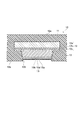
図1は、本実施形態に係る半導体装置を示す断面図である。
図2は、本実施形態に係る半導体装置の再配線層の一部を示す一部拡大断面図である。
Hereinafter, embodiments will be described.
FIG. 1 is a cross-sectional view showing the semiconductor device according to the present embodiment.
FIG. 2 is a partially enlarged sectional view showing a part of the rewiring layer of the semiconductor device according to the present embodiment.
図1に示すように、本実施形態に係る半導体装置1においては、再配線層10が設けられている。再配線層10においては、母材として、例えば有機材料からなる絶縁層11が設けられている。また、再配線層10においては、絶縁層11内に、複数の配線12、複数のビア13、複数のビア14及び複数の電極層15が設けられている。
As shown in FIG. 1, in the
配線12は、例えば金属材料からなり、絶縁層11内に埋め込まれている。ビア13は、例えば銅(Cu)等の金属材料からなり、絶縁層11内に配置されており、配線12に接続されている。以下、本明細書においては、配線12からビア13に向かう方向を「下」といい、その反対方向を「上」という。すなわち、ビア13は配線12よりも下方に配置されている。ビア14は、金属材料、例えば貴金属、例えば、ニッケル(Ni)層、パラジウム(Pd)層及び金(Au)層の積層体からなり、絶縁層11内において、配線12よりも上方に配置されており、配線12に接続されている。ビア14は、再配線層10の上面10aにおいて露出している。
The
電極層15は、絶縁層11内において、ビア13の下面上に配置されており、ビア13に接続されている。電極層15は、再配線層10の下面10bにおいて露出している。電極層15は、ビア13の材料とは異なる金属材料からなり、例えば貴金属を含む。電極層15の厚さは、例えば、数μm(ミクロン)である。
The
また、半導体装置1においては、再配線層10上に複数の半導体チップ20が設けられており、上下方向に沿って積層されている。半導体チップ20は、例えば、3次元NAND型のメモリチップである。再配線層10のビア14と最下段の半導体チップ20とは、マイクロバンプ21により接合されている。また、隣り合う半導体チップ20同士は、マイクロバンプ22により接合されている。なお、本明細書において「接合されている」とは、機械的に連結されていると共に電気的に接続されている状態をいう。再配線層10の上面10a上には、樹脂部材24が設けられている。樹脂部材24は樹脂材料からなり、積層された半導体チップ20、マイクロバンプ21及び22を覆っている。
In the
半導体装置1において、再配線層10の下面10b上には、バンプ26が設けられている。バンプ26は例えば半田からなり、その直径はマイクロバンプ21及び22の直径よりも大きく、例えば数百μmである。バンプ26は電極層15の下面15a(図2参照)に接合されている。
In the
また、再配線層10の下面10b上には、制御用チップ27が搭載されている。制御用チップ27は、マイクロバンプ28を介して、再配線層10の電極層15に接合されている。すなわち、複数の電極層15のうちの一部はバンプ26に接合されており、他の一部はマイクロバンプ28に接合されている。また、再配線層10と制御用チップ27との間には、マイクロバンプ28を覆う樹脂部材29が設けられている。
A
半導体装置1においては、各半導体チップ20の電極(図示せず)が、マイクロバンプ22及び21、ビア14、配線12、ビア13、電極層15及びバンプ26を介して、外部に接続される。そして、制御用チップ27は、例えば、複数の半導体チップ20と外部との間の信号のやりとりを制御するインターフェイスとして機能すると共に、これらの半導体チップ20の動作を制御するコントローラーとして機能する。
In the
図2に示すように、配線12においては、例えば銅からなる本体部12aが設けられており、本体部12aの下面上に銅層12b及びチタン層12cが設けられている。一方、電極層15及びビア13からなる積層体の形状は、逆四角錐台形状である。すなわち、電極層15に近いほど、幅が狭くなっている。電極層15においては、ビア13側から順に、ニッケル層15b及び金属間化合物層15cが積層されている。ニッケル層15bはビア13に接し、金属間化合物層15cはバンプ26に接している。金属間化合物層15cは、例えば、銅、錫(Sn)及びニッケル(Ni)を主成分とする金属間化合物からなり、パラジウム(Pd)及び金(Au)等の貴金属を含んでいてもよい。
As shown in FIG. 2, in the
電極層15と再配線層10の上面10aとの距離L1は、再配線層10の厚さ、すなわち、再配線層10の下面10bと上面10aとの距離L2よりも短い。すなわち、L1<L2である。また、電極層15の下面15a、すなわち、バンプ26側の表面は、再配線層10の下面10bに対して凹んでいる。なお、電極層15の下面15aは、再配線層10の下面10bと同一面を構成していてもよい。換言すれば、電極層15の下面15aと再配線層10の上面10aとの距離L3は、上述の距離L2以下である。すなわち、L3≦L2である。
The distance L1 between the
次に、本実施形態に係る半導体装置の製造方法について説明する。
図3(a)〜(d)、図4(a)〜(c)、図5(a)〜(c)、図6(a)〜(c)、図7(a)及び(b)は、本実施形態に係る半導体装置の製造方法を示す断面図である。
図8は、本実施形態に係る半導体装置の製造方法を示す一部拡大断面図である。
Next, a method for manufacturing the semiconductor device according to the present embodiment will be described.
3 (a)-(d), 4 (a)-(c), 5 (a)-(c), 6 (a)-(c), 7 (a) and 7 (b) FIG. 5 is a cross-sectional view showing the method for manufacturing the semiconductor device according to the embodiment.
FIG. 8 is a partially enlarged cross-sectional view illustrating the method for manufacturing the semiconductor device according to the present embodiment.
先ず、図3(a)に示すように、支持基板100を用意する。支持基板100は、例えば、シリコンウェーハ又はガラス基板である。次に、支持基板100の上面上に剥離層101を形成する。剥離層101は、例えば、特定の薬液に溶解可能な有機材料、光照射によって分解反応を生じる有機材料、又は、一定以上の応力印加で剥離を生じる有機材料若しくは無機材料からなる。次に、剥離層101上にチタン(Ti)層102を形成し、その上に銅層103を形成する。チタン層102は支持基板100との密着性が高い。チタン層102及び銅層103により、シード層104が構成される。
First, as shown in FIG. 3A, a
次に、図3(b)に示すように、シード層104上に、例えば有機材料からなる絶縁層11aを形成する。次に、例えばリソグラフィ法又はレーザー照射により、絶縁層11aにビアホール11bを形成する。ビアホール11bの底面には、シード層104が露出する。
Next, as illustrated in FIG. 3B, an insulating
次に、図3(c)に示すように、シード層104を介して電解めっきを行い、ビアホール11b内に金属材料、例えば、銅を埋め込み、ビア13を形成する。このとき、銅層103は導電性が高いため、後述するレジストパターン105が広範囲に形成された場合に、電解めっきの厚さを均一化しやすい。
Next, as shown in FIG. 3C, electrolytic plating is performed through the
次に、図3(d)に示すように、絶縁層11a上にチタン層12c及び銅層12bを形成する。次に、銅層12b上にレジストパターン105を形成する。レジストパターン105には、リソグラフィ法により、開口部105aを形成する。開口部105aの底面には、銅層12bが露出する。次に、チタン層12c及び銅層12bをシード層として電解めっきを行い、開口部105a内に銅を埋め込み、本体部12aを形成する。次に、レジストパターン105を除去する。次に、エッチングを行い、銅層12b及びチタン層12cにおける本体部12aによって覆われていない部分を除去する。これにより、銅層12b及びチタン層12cが、上方から見て本体部12aと同じ形状にパターニングされる。本体部12a、並びに、パターニングされた銅層12b及びチタン層12cにより、配線12が形成される。配線12はビア13に接続される。
Next, as shown in FIG. 3D, a
次に、図4(a)に示すように、絶縁層11a及び配線12上に、例えば有機材料からなる絶縁層11cを形成する。絶縁層11a及び絶縁層11cにより、絶縁層11が形成される。次に、例えばリソグラフィ法又はレーザー照射により、絶縁層11cにビアホール11dを形成する。ビアホール11dの底面には、配線12が露出する。
Next, as illustrated in FIG. 4A, an insulating
次に、図4(b)に示すように、無電解めっき法により、配線12の露出面上に、貴金属を含む金属材料、例えば、ニッケル層、パラジウム層及び金層をこの順に形成する。これにより、ビアホール11d内にビア14が形成される。ビア14は、配線12に接続されると共に、絶縁層11aの上面において露出する。
Next, as shown in FIG. 4B, a metal material containing a noble metal, for example, a nickel layer, a palladium layer, and a gold layer is formed in this order on the exposed surface of the
次に、図4(c)に示すように、ビア14上にマイクロバンプ21を介して半導体チップ20を接合する。次に、この半導体チップ20上に、複数の半導体チップ20をマイクロバンプ22を介して積層する。これにより、絶縁層11上に、複数の半導体チップ20が積層される。複数の半導体チップ20の電極(図示せず)は、マイクロバンプ22及び21を介して、ビア14に接続される。なお、予めマイクロバンプ22を介して相互に接合させた複数の半導体チップ20からなる積層体を、マイクロバンプ21を介してビア14に接合してもよい。
Next, as shown in FIG. 4C, the
次に、図5(a)に示すように、絶縁層11上に、複数の半導体チップ20からなる積層体を覆うように樹脂材料を成形封止し、例えば200℃以下の温度で熱硬化させることにより、樹脂部材24を形成する。
Next, as shown in FIG. 5A, a resin material is molded and sealed on the insulating
次に、図5(b)に示すように、例えば薬液を用いて溶解させることにより、若しくは、光照射により剥離層を分解することにより、剥離層101を除去する。又は、剥離層101の密着力を上回る力で支持基板100を剥離層101から引き剥がす。これにより、支持基板100が除去されて、シード層104が露出する。
Next, as shown in FIG. 5B, the
次に、図5(c)に示すように、シード層104上に剥離層101の残渣(図示せず)が残留していれば、これを除去する。次に、例えばウェットエッチング法により、シード層104を除去する。これにより、絶縁層11及びビア13が露出する。
Next, as shown in FIG. 5C, if a residue (not shown) of the
次に、図6(a)に示すように、例えばウェットエッチング法により、ビア13の露出面をエッチングする。これにより、ビア13の一部が除去され、絶縁層11の下面に凹部106が形成される。凹部106の底面にはビア13の残部が露出する。凹部106の深さは、例えば数μmとする。なお、ビア13の材料を銅とした場合には、銅のエッチング液による処理条件を制御することで、銅層103の全面除去とビア13の一部除去を1回のウェットエッチング処理で実施可能である。
Next, as shown in FIG. 6A, the exposed surface of the via 13 is etched by, for example, a wet etching method. As a result, a part of the via 13 is removed, and a
次に、図6(b)及び図8に示すように、例えば無電解めっき法により、ビア13の露出面に、ビア13の材料とは異なる金属材料、例えば貴金属を含む金属材料、例えば、ニッケル層15b、パラジウム層15d及び金層15eをこの順に形成する。これにより、凹部106内に電極層15が形成される。このとき、電極層15の厚さがビア13の除去厚、すなわち、凹部106の深さを超えないように、電極材料の成長条件、例えば温度や処理時間を制御する。絶縁層11、配線12、ビア13、ビア14及び電極層15により、再配線層10が形成される。電極層15の下面15aは、再配線層10の下面10bに対して凹んでいるか、同一面である。
Next, as shown in FIGS. 6B and 8, a metal material different from the material of the via 13, for example, a metal material containing noble metal, for example, nickel, on the exposed surface of the via 13, for example, by electroless plating. The
次に、図6(c)に示すように、一部の電極層15に、マイクロバンプ28を介して、制御用チップ27を接合する。次に、再配線層10と制御用チップ27との間に、マイクロバンプ28を覆うように、樹脂部材29を形成する。
Next, as shown in FIG. 6C, the
次に、図7(a)に示すように、マイクロバンプ28が接合されていない電極層15に、例えば半田からなるバンプ26を接合する。このとき、図8及び図2に示すように、バンプ26が接合された電極層15においては、金層15e及びパラジウム層15dがバンプ26内に拡散して消失する。一方、ニッケル層15bとバンプ26との間には、銅、錫及びニッケルを主成分とする金属間化合物層15cが形成される。
Next, as shown in FIG. 7A, a
次に、図7(b)に示すように、ダイシングを行い、再配線層10及び樹脂部材24を切断する。これにより、複数の半導体装置1が製造される。
Next, as shown in FIG. 7B, dicing is performed to cut the
次に、本実施形態の効果について説明する。
本実施形態においては、図3(a)〜図5(a)に示す工程において、支持基板100上に絶縁層11、半導体チップ20からなる積層体、樹脂部材24等からなる構造体を形成した後、図5(b)に示す工程において、支持基板100を除去している。また、図5(c)〜図7(a)に示す工程において、電極層15及びバンプ26を形成している。これにより、再配線層10を介して半導体チップ20をバンプ26に接続することができる。この結果、プリント基板を用いる場合と比較して、半導体装置1の低背化を図ることができる。
Next, the effect of this embodiment will be described.
In the present embodiment, in the steps shown in FIGS. 3A to 5A, a structure made of the insulating
また、図5(b)に示す工程において支持基板100を除去すると、主として半導体チップ20において発生する応力、及び、樹脂部材24を熱硬化させたときの応力により、絶縁層11、半導体チップ20からなる積層体、樹脂部材24等からなる構造体に反りが発生する場合がある。反りが発生すると、ビア13の位置が設計位置からずれてしまう。しかしながら、本実施形態においては、図6(a)に示す工程において、ビア13をエッチングすることにより凹部106を形成し、図6(b)に示す工程において、凹部106内に無電解めっき法により、電極層15を形成している。このように、本実施形態においては、ビア13の位置がずれた場合でも、電極層15を自己整合的に形成できるため、電極層15の位置精度が高い。また、電極層15が凹部106内に形成されるため、電極層15の形成に伴って電極層15同士が近づくことがなく、電極層15間の短絡を抑制できる。
5B, when the
これに対して、仮に、例えばリソグラフィ法及びRIE(Reactive Ion Etching:反応性イオンエッチング)法等により、ビア13とは独立に電極層15を形成しようとすると、構造体の反りによってビア13の位置がずれた場合には、電極層15とビア13との位置合わせが困難になる。また、仮に、凹部106を形成せずに電極層15を形成すると、電極層15の成長に伴って電極層15が水平方向にも拡がるため、電極層15同士が近づき、短絡する可能性がある。電極層15同士の短絡を確実に防止するためには、設計段階において、電極層15間の距離を十分に長くしておく必要があり、半導体装置1の小型化が阻害されてしまう。
On the other hand, if the
以上説明した実施形態によれば、電極層の位置精度が高い半導体装置及びその製造方法を実現することができる。 According to the embodiment described above, it is possible to realize a semiconductor device having a high positional accuracy of the electrode layer and a manufacturing method thereof.
以上、本発明のいくつかの実施形態を説明したが、これらの実施形態は、例として提示したものであり、発明の範囲を限定することは意図していない。これら新規な実施形態は、その他の様々な形態で実施されることが可能であり、発明の要旨を逸脱しない範囲で、種々の省略、置き換え、変更を行うことができる。これら実施形態やその変形は、発明の範囲や要旨に含まれるとともに、特許請求の範囲に記載された発明及びその等価物の範囲に含まれる。 As mentioned above, although some embodiment of this invention was described, these embodiment is shown as an example and is not intending limiting the range of invention. These novel embodiments can be implemented in various other forms, and various omissions, replacements, and changes can be made without departing from the scope of the invention. These embodiments and modifications thereof are included in the scope and gist of the invention, and are included in the scope of the invention described in the claims and the equivalents thereof.
1:半導体装置
10:再配線層
10a:上面
10b:下面
11:絶縁層
11a:絶縁層
11b:ビアホール
11c:絶縁層
11d:ビアホール
12:配線
12a:本体部
12b:銅層
12c:チタン層
13:ビア
14:ビア
15:電極層
15a:下面
15b:ニッケル層
15c:金属間化合物層
15d:パラジウム層
15e:金層
20:半導体チップ
21、22:マイクロバンプ
24:樹脂部材
26:バンプ
27:制御用チップ
28:マイクロバンプ
29:樹脂部材
100:支持基板
101:剥離層
102:チタン層
103:銅層
104:シード層
105:レジストパターン
105a:開口部
106:凹部
L1、L2、L3:距離
1: Semiconductor device 10:
Claims (6)
前記再配線層の第1面上に設けられた複数のバンプと、
前記再配線層の第2面上に積層された複数のチップと、
前記第2面上に設けられ、前記複数のチップを覆う樹脂部材と、
を備え、
前記再配線層は、
絶縁層と、
前記絶縁層内に設けられた配線と、
前記絶縁層内に設けられ、前記配線に接続された第1ビアと、
前記絶縁層内に設けられ、前記第1ビアの材料とは異なる金属材料によって形成され、前記第1面において露出し、前記第1ビア及び前記バンプに接続された電極層と、
前記絶縁層内に設けられ、前記配線及び前記複数のチップに接続された第2ビアと、
を有し、
前記電極層と前記第2面との距離は、前記第1面と前記第2面との距離よりも短い半導体装置。 A rewiring layer;
A plurality of bumps provided on the first surface of the redistribution layer;
A plurality of chips stacked on the second surface of the redistribution layer;
A resin member provided on the second surface and covering the plurality of chips;
With
The rewiring layer is
An insulating layer;
Wiring provided in the insulating layer;
A first via provided in the insulating layer and connected to the wiring;
An electrode layer provided in the insulating layer, formed of a metal material different from the material of the first via, exposed on the first surface, and connected to the first via and the bump;
A second via provided in the insulating layer and connected to the wiring and the plurality of chips;
Have
A distance between the electrode layer and the second surface is a semiconductor device shorter than a distance between the first surface and the second surface.
前記絶縁層上に複数のチップを積層すると共に、前記複数のチップを前記第2ビアに接続する工程と、
前記絶縁層上に、前記複数のチップを覆う樹脂部材を形成する工程と、
前記支持基板を除去する工程と、
前記第1ビアの露出面をエッチングすることにより、前記絶縁層の下面に凹部を形成する工程と、
前記凹部内に、前記第1ビアの材料とは異なる金属材料からなる電極層を形成する工程と、
前記電極層にバンプを接合する工程と、
を備えた半導体装置の製造方法。 On the support substrate, an insulating layer, a plurality of first vias provided in the insulating layer and exposed on a lower surface of the insulating layer, a plurality of first vias provided in the insulating layer and connected to the plurality of first vias Forming a plurality of second vias that are connected to the wiring and exposed on the upper surface of the insulating layer;
Stacking a plurality of chips on the insulating layer and connecting the plurality of chips to the second via;
Forming a resin member covering the plurality of chips on the insulating layer;
Removing the support substrate;
Etching the exposed surface of the first via to form a recess in the lower surface of the insulating layer;
Forming an electrode layer made of a metal material different from the material of the first via in the recess;
Bonding bumps to the electrode layer;
A method for manufacturing a semiconductor device comprising:
Priority Applications (4)
| Application Number | Priority Date | Filing Date | Title |
|---|---|---|---|
| JP2018034557A JP2019149507A (en) | 2018-02-28 | 2018-02-28 | Semiconductor device and manufacturing method thereof |
| TW107122932A TWI721286B (en) | 2018-02-28 | 2018-07-03 | Semiconductor device and manufacturing method thereof |
| CN201810832374.8A CN110211943A (en) | 2018-02-28 | 2018-07-26 | Semiconductor device and its manufacturing method |
| US16/058,161 US10658338B2 (en) | 2018-02-28 | 2018-08-08 | Semiconductor device including a re-interconnection layer and method for manufacturing same |
Applications Claiming Priority (1)
| Application Number | Priority Date | Filing Date | Title |
|---|---|---|---|
| JP2018034557A JP2019149507A (en) | 2018-02-28 | 2018-02-28 | Semiconductor device and manufacturing method thereof |
Publications (1)
| Publication Number | Publication Date |
|---|---|
| JP2019149507A true JP2019149507A (en) | 2019-09-05 |
Family
ID=67686099
Family Applications (1)
| Application Number | Title | Priority Date | Filing Date |
|---|---|---|---|
| JP2018034557A Pending JP2019149507A (en) | 2018-02-28 | 2018-02-28 | Semiconductor device and manufacturing method thereof |
Country Status (4)
| Country | Link |
|---|---|
| US (1) | US10658338B2 (en) |
| JP (1) | JP2019149507A (en) |
| CN (1) | CN110211943A (en) |
| TW (1) | TWI721286B (en) |
Cited By (1)
| Publication number | Priority date | Publication date | Assignee | Title |
|---|---|---|---|---|
| US11270934B2 (en) | 2018-03-13 | 2022-03-08 | Kabushiki Kaisha Toshiba | Semiconductor device and method for manufacturing same |
Families Citing this family (3)
| Publication number | Priority date | Publication date | Assignee | Title |
|---|---|---|---|---|
| US10950531B2 (en) | 2019-05-30 | 2021-03-16 | Advanced Semiconductor Engineering, Inc. | Semiconductor device package and method of manufacturing the same |
| KR20210084736A (en) * | 2019-12-27 | 2021-07-08 | 삼성전자주식회사 | Semiconductor package |
| JP2022020377A (en) * | 2020-07-20 | 2022-02-01 | キオクシア株式会社 | Semiconductor device and manufacturing method of semiconductor device |
Family Cites Families (14)
| Publication number | Priority date | Publication date | Assignee | Title |
|---|---|---|---|---|
| US20070126085A1 (en) | 2005-12-02 | 2007-06-07 | Nec Electronics Corporation | Semiconductor device and method of manufacturing the same |
| JP2007180529A (en) | 2005-12-02 | 2007-07-12 | Nec Electronics Corp | Semiconductor device and method of manufacturing the same |
| JP5032187B2 (en) * | 2007-04-17 | 2012-09-26 | 新光電気工業株式会社 | Wiring substrate manufacturing method, semiconductor device manufacturing method, and wiring substrate |
| US8039303B2 (en) * | 2008-06-11 | 2011-10-18 | Stats Chippac, Ltd. | Method of forming stress relief layer between die and interconnect structure |
| US8799845B2 (en) * | 2010-02-16 | 2014-08-05 | Deca Technologies Inc. | Adaptive patterning for panelized packaging |
| US8259464B2 (en) * | 2010-06-24 | 2012-09-04 | Maxim Integrated Products, Inc. | Wafer level package (WLP) device having bump assemblies including a barrier metal |
| US10204879B2 (en) * | 2011-01-21 | 2019-02-12 | STATS ChipPAC Pte. Ltd. | Semiconductor device and method of forming wafer-level interconnect structures with advanced dielectric characteristics |
| US8754514B2 (en) * | 2011-08-10 | 2014-06-17 | Taiwan Semiconductor Manufacturing Company, Ltd. | Multi-chip wafer level package |
| JP5942823B2 (en) | 2012-12-03 | 2016-06-29 | 富士通株式会社 | Electronic component device manufacturing method, electronic component device, and electronic device |
| JP2016062995A (en) | 2014-09-16 | 2016-04-25 | 株式会社東芝 | Semiconductor device and method of manufacturing semiconductor device |
| JP2016127239A (en) | 2015-01-08 | 2016-07-11 | マイクロン テクノロジー, インク. | Semiconductor device manufacturing method |
| US9659907B2 (en) * | 2015-04-07 | 2017-05-23 | Apple Inc. | Double side mounting memory integration in thin low warpage fanout package |
| US10797038B2 (en) * | 2016-02-25 | 2020-10-06 | Taiwan Semiconductor Manufacturing Company, Ltd. | Semiconductor package and rework process for the same |
| US9659911B1 (en) * | 2016-04-20 | 2017-05-23 | Powertech Technology Inc. | Package structure and manufacturing method thereof |
-
2018
- 2018-02-28 JP JP2018034557A patent/JP2019149507A/en active Pending
- 2018-07-03 TW TW107122932A patent/TWI721286B/en active
- 2018-07-26 CN CN201810832374.8A patent/CN110211943A/en active Pending
- 2018-08-08 US US16/058,161 patent/US10658338B2/en active Active
Cited By (1)
| Publication number | Priority date | Publication date | Assignee | Title |
|---|---|---|---|---|
| US11270934B2 (en) | 2018-03-13 | 2022-03-08 | Kabushiki Kaisha Toshiba | Semiconductor device and method for manufacturing same |
Also Published As
| Publication number | Publication date |
|---|---|
| US10658338B2 (en) | 2020-05-19 |
| TWI721286B (en) | 2021-03-11 |
| US20190267350A1 (en) | 2019-08-29 |
| TW201937734A (en) | 2019-09-16 |
| CN110211943A (en) | 2019-09-06 |
Similar Documents
| Publication | Publication Date | Title |
|---|---|---|
| TWI683378B (en) | Semicondcutor package and manufacturing method thereof | |
| JP5222459B2 (en) | Semiconductor chip manufacturing method, multichip package | |
| JP4343044B2 (en) | Interposer, manufacturing method thereof, and semiconductor device | |
| JP5808586B2 (en) | Manufacturing method of interposer | |
| US20200370184A1 (en) | Fabrication method of substrate having electrical interconnection structures | |
| US9711403B2 (en) | Method for forming chip package | |
| US20090283872A1 (en) | Package structure of three-dimensional stacking dice and method for manufacturing the same | |
| JP2005327984A (en) | Electronic component and method of manufacturing electronic-component mounting structure | |
| US10580739B2 (en) | Package substrate and associated fabrication method with varying depths for circuit device terminals | |
| JP2019149507A (en) | Semiconductor device and manufacturing method thereof | |
| JP2007180529A (en) | Semiconductor device and method of manufacturing the same | |
| TW202032679A (en) | Package structure and methods of forming the same | |
| KR101708535B1 (en) | Integrated circuit apparatus and method for manufacturing the same | |
| JP5026025B2 (en) | Semiconductor device | |
| CN110943067B (en) | Semiconductor device and method for manufacturing the same | |
| JP2019161003A (en) | Semiconductor device and manufacturing method thereof | |
| CN109326574B (en) | Substrate structure, semiconductor package including the same, and method of manufacturing the same | |
| US8232639B2 (en) | Semiconductor-device mounted board and method of manufacturing the same | |
| JP2006041512A (en) | Method of manufacturing integrated-circuit chip for multi-chip package, and wafer and chip formed by the method thereof | |
| US8258009B2 (en) | Circuit substrate and manufacturing method thereof and package structure and manufacturing method thereof | |
| US11282775B1 (en) | Chip package assembly with stress decoupled interconnect layer | |
| KR20190091095A (en) | Semiconductor package and method of manufacturinng the same | |
| JP2011238742A (en) | Method for manufacturing a wiring substrate and the wiring substrate | |
| TWI765455B (en) | Semiconductor packages and method of manufacturing the same | |
| KR101101432B1 (en) | Fabrication method of semiconductor device and semiconductor device using the same |
Legal Events
| Date | Code | Title | Description |
|---|---|---|---|
| A711 | Notification of change in applicant |
Free format text: JAPANESE INTERMEDIATE CODE: A712 Effective date: 20180905 |