KR20160117260A - Light Irradiation Module - Google Patents
Light Irradiation Module Download PDFInfo
- Publication number
- KR20160117260A KR20160117260A KR1020160037006A KR20160037006A KR20160117260A KR 20160117260 A KR20160117260 A KR 20160117260A KR 1020160037006 A KR1020160037006 A KR 1020160037006A KR 20160037006 A KR20160037006 A KR 20160037006A KR 20160117260 A KR20160117260 A KR 20160117260A
- Authority
- KR
- South Korea
- Prior art keywords
- metal base
- substrate
- light irradiation
- led chips
- irradiation module
- Prior art date
Links
Images


Classifications
-
- H—ELECTRICITY
- H01—ELECTRIC ELEMENTS
- H01L—SEMICONDUCTOR DEVICES NOT COVERED BY CLASS H10
- H01L27/00—Devices consisting of a plurality of semiconductor or other solid-state components formed in or on a common substrate
- H01L27/02—Devices consisting of a plurality of semiconductor or other solid-state components formed in or on a common substrate including semiconductor components specially adapted for rectifying, oscillating, amplifying or switching and having at least one potential-jump barrier or surface barrier; including integrated passive circuit elements with at least one potential-jump barrier or surface barrier
- H01L27/12—Devices consisting of a plurality of semiconductor or other solid-state components formed in or on a common substrate including semiconductor components specially adapted for rectifying, oscillating, amplifying or switching and having at least one potential-jump barrier or surface barrier; including integrated passive circuit elements with at least one potential-jump barrier or surface barrier the substrate being other than a semiconductor body, e.g. an insulating body
-
- H—ELECTRICITY
- H01—ELECTRIC ELEMENTS
- H01L—SEMICONDUCTOR DEVICES NOT COVERED BY CLASS H10
- H01L33/00—Semiconductor devices with at least one potential-jump barrier or surface barrier specially adapted for light emission; Processes or apparatus specially adapted for the manufacture or treatment thereof or of parts thereof; Details thereof
-
- H—ELECTRICITY
- H01—ELECTRIC ELEMENTS
- H01L—SEMICONDUCTOR DEVICES NOT COVERED BY CLASS H10
- H01L25/00—Assemblies consisting of a plurality of individual semiconductor or other solid state devices ; Multistep manufacturing processes thereof
- H01L25/03—Assemblies consisting of a plurality of individual semiconductor or other solid state devices ; Multistep manufacturing processes thereof all the devices being of a type provided for in the same subgroup of groups H01L27/00 - H01L33/00, or in a single subclass of H10K, H10N, e.g. assemblies of rectifier diodes
- H01L25/04—Assemblies consisting of a plurality of individual semiconductor or other solid state devices ; Multistep manufacturing processes thereof all the devices being of a type provided for in the same subgroup of groups H01L27/00 - H01L33/00, or in a single subclass of H10K, H10N, e.g. assemblies of rectifier diodes the devices not having separate containers
- H01L25/075—Assemblies consisting of a plurality of individual semiconductor or other solid state devices ; Multistep manufacturing processes thereof all the devices being of a type provided for in the same subgroup of groups H01L27/00 - H01L33/00, or in a single subclass of H10K, H10N, e.g. assemblies of rectifier diodes the devices not having separate containers the devices being of a type provided for in group H01L33/00
- H01L25/0753—Assemblies consisting of a plurality of individual semiconductor or other solid state devices ; Multistep manufacturing processes thereof all the devices being of a type provided for in the same subgroup of groups H01L27/00 - H01L33/00, or in a single subclass of H10K, H10N, e.g. assemblies of rectifier diodes the devices not having separate containers the devices being of a type provided for in group H01L33/00 the devices being arranged next to each other
-
- H—ELECTRICITY
- H01—ELECTRIC ELEMENTS
- H01L—SEMICONDUCTOR DEVICES NOT COVERED BY CLASS H10
- H01L27/00—Devices consisting of a plurality of semiconductor or other solid-state components formed in or on a common substrate
- H01L27/15—Devices consisting of a plurality of semiconductor or other solid-state components formed in or on a common substrate including semiconductor components with at least one potential-jump barrier or surface barrier specially adapted for light emission
- H01L27/153—Devices consisting of a plurality of semiconductor or other solid-state components formed in or on a common substrate including semiconductor components with at least one potential-jump barrier or surface barrier specially adapted for light emission in a repetitive configuration, e.g. LED bars
- H01L27/156—Devices consisting of a plurality of semiconductor or other solid-state components formed in or on a common substrate including semiconductor components with at least one potential-jump barrier or surface barrier specially adapted for light emission in a repetitive configuration, e.g. LED bars two-dimensional arrays
-
- H—ELECTRICITY
- H01—ELECTRIC ELEMENTS
- H01L—SEMICONDUCTOR DEVICES NOT COVERED BY CLASS H10
- H01L33/00—Semiconductor devices with at least one potential-jump barrier or surface barrier specially adapted for light emission; Processes or apparatus specially adapted for the manufacture or treatment thereof or of parts thereof; Details thereof
- H01L33/02—Semiconductor devices with at least one potential-jump barrier or surface barrier specially adapted for light emission; Processes or apparatus specially adapted for the manufacture or treatment thereof or of parts thereof; Details thereof characterised by the semiconductor bodies
-
- H—ELECTRICITY
- H01—ELECTRIC ELEMENTS
- H01L—SEMICONDUCTOR DEVICES NOT COVERED BY CLASS H10
- H01L33/00—Semiconductor devices with at least one potential-jump barrier or surface barrier specially adapted for light emission; Processes or apparatus specially adapted for the manufacture or treatment thereof or of parts thereof; Details thereof
- H01L33/48—Semiconductor devices with at least one potential-jump barrier or surface barrier specially adapted for light emission; Processes or apparatus specially adapted for the manufacture or treatment thereof or of parts thereof; Details thereof characterised by the semiconductor body packages
- H01L33/62—Arrangements for conducting electric current to or from the semiconductor body, e.g. lead-frames, wire-bonds or solder balls
-
- H—ELECTRICITY
- H01—ELECTRIC ELEMENTS
- H01L—SEMICONDUCTOR DEVICES NOT COVERED BY CLASS H10
- H01L33/00—Semiconductor devices with at least one potential-jump barrier or surface barrier specially adapted for light emission; Processes or apparatus specially adapted for the manufacture or treatment thereof or of parts thereof; Details thereof
- H01L33/48—Semiconductor devices with at least one potential-jump barrier or surface barrier specially adapted for light emission; Processes or apparatus specially adapted for the manufacture or treatment thereof or of parts thereof; Details thereof characterised by the semiconductor body packages
- H01L33/64—Heat extraction or cooling elements
-
- H—ELECTRICITY
- H01—ELECTRIC ELEMENTS
- H01L—SEMICONDUCTOR DEVICES NOT COVERED BY CLASS H10
- H01L2224/00—Indexing scheme for arrangements for connecting or disconnecting semiconductor or solid-state bodies and methods related thereto as covered by H01L24/00
- H01L2224/01—Means for bonding being attached to, or being formed on, the surface to be connected, e.g. chip-to-package, die-attach, "first-level" interconnects; Manufacturing methods related thereto
- H01L2224/42—Wire connectors; Manufacturing methods related thereto
- H01L2224/47—Structure, shape, material or disposition of the wire connectors after the connecting process
- H01L2224/48—Structure, shape, material or disposition of the wire connectors after the connecting process of an individual wire connector
- H01L2224/4805—Shape
- H01L2224/4809—Loop shape
- H01L2224/48091—Arched
-
- H—ELECTRICITY
- H01—ELECTRIC ELEMENTS
- H01L—SEMICONDUCTOR DEVICES NOT COVERED BY CLASS H10
- H01L2224/00—Indexing scheme for arrangements for connecting or disconnecting semiconductor or solid-state bodies and methods related thereto as covered by H01L24/00
- H01L2224/01—Means for bonding being attached to, or being formed on, the surface to be connected, e.g. chip-to-package, die-attach, "first-level" interconnects; Manufacturing methods related thereto
- H01L2224/42—Wire connectors; Manufacturing methods related thereto
- H01L2224/47—Structure, shape, material or disposition of the wire connectors after the connecting process
- H01L2224/49—Structure, shape, material or disposition of the wire connectors after the connecting process of a plurality of wire connectors
- H01L2224/491—Disposition
- H01L2224/4911—Disposition the connectors being bonded to at least one common bonding area, e.g. daisy chain
- H01L2224/49111—Disposition the connectors being bonded to at least one common bonding area, e.g. daisy chain the connectors connecting two common bonding areas, e.g. Litz or braid wires
-
- H—ELECTRICITY
- H01—ELECTRIC ELEMENTS
- H01L—SEMICONDUCTOR DEVICES NOT COVERED BY CLASS H10
- H01L2224/00—Indexing scheme for arrangements for connecting or disconnecting semiconductor or solid-state bodies and methods related thereto as covered by H01L24/00
- H01L2224/01—Means for bonding being attached to, or being formed on, the surface to be connected, e.g. chip-to-package, die-attach, "first-level" interconnects; Manufacturing methods related thereto
- H01L2224/42—Wire connectors; Manufacturing methods related thereto
- H01L2224/47—Structure, shape, material or disposition of the wire connectors after the connecting process
- H01L2224/49—Structure, shape, material or disposition of the wire connectors after the connecting process of a plurality of wire connectors
- H01L2224/491—Disposition
- H01L2224/4912—Layout
- H01L2224/49175—Parallel arrangements
-
- H—ELECTRICITY
- H01—ELECTRIC ELEMENTS
- H01L—SEMICONDUCTOR DEVICES NOT COVERED BY CLASS H10
- H01L2924/00—Indexing scheme for arrangements or methods for connecting or disconnecting semiconductor or solid-state bodies as covered by H01L24/00
- H01L2924/10—Details of semiconductor or other solid state devices to be connected
- H01L2924/11—Device type
- H01L2924/12—Passive devices, e.g. 2 terminal devices
- H01L2924/1204—Optical Diode
- H01L2924/12041—LED
-
- H—ELECTRICITY
- H01—ELECTRIC ELEMENTS
- H01L—SEMICONDUCTOR DEVICES NOT COVERED BY CLASS H10
- H01L2924/00—Indexing scheme for arrangements or methods for connecting or disconnecting semiconductor or solid-state bodies as covered by H01L24/00
- H01L2924/19—Details of hybrid assemblies other than the semiconductor or other solid state devices to be connected
- H01L2924/191—Disposition
- H01L2924/19101—Disposition of discrete passive components
- H01L2924/19107—Disposition of discrete passive components off-chip wires
Abstract
Description
본 발명은, 예를 들면, 자외선 조사장치 등에 탑재되는 광 조사 모듈에 관한 것으로서, 특히, LED(Light Emitting Diode) 등의 발광 소자를 이용한 광 조사 모듈에 관한 것이다.BACKGROUND OF THE INVENTION 1. Field of the Invention The present invention relates to a light irradiation module mounted on, for example, an ultraviolet irradiation device, and more particularly to a light irradiation module using a light emitting device such as an LED (Light Emitting Diode).
종래, FPD(Flat Panel Display) 주위의 접착제로서 이용되는 자외선 경화 수지나, 오프셋 매엽 인쇄용 잉크로서 이용되는 자외선 경화형 잉크를 경화시키기 위해, 자외광 조사장치가 이용되고 있다.BACKGROUND ART [0002] Conventionally, an ultraviolet light irradiation apparatus has been used to cure an ultraviolet curable resin used as an adhesive around an FPD (Flat Panel Display) or an ultraviolet curable ink used as an offset sheet laminating ink.
자외광 조사장치로서는, 종래, 고압 수은 램프나 수은 크세논 램프 등을 광원으로 하는 램프형 조사장치가 알려져 있지만, 최근, 소비 전력의 삭감, 장수명화, 장치 사이즈의 컴팩트화에 대한 요청으로 인해, 종래의 방전 램프 대신에, 자외 LED(Light Emitting Diode)를 광원으로서 이용한 자외광 조사장치가 개발되고 있다(예를 들면, 특허문헌 1).As a ultraviolet irradiator, a lamp-type irradiator having a high-pressure mercury lamp or a mercury xenon lamp as a light source has been conventionally known. However, recently, due to demands for reduction in power consumption, longevity, An ultraviolet light irradiating device using an ultraviolet LED (Light Emitting Diode) as a light source has been developed (for example, Patent Document 1).
특허문헌 1에 기재된 자외광 조사장치는, 기판(기체), 및 기판 상에 2차원으로 배치된 다수의 자외 LED를 구비하고 있으며, 이에 의해 강한 조사 강도의 자외광을 얻고 있다.The ultraviolet light irradiation apparatus described in Patent Document 1 has a substrate (base) and a plurality of ultraviolet LEDs arranged two-dimensionally on the substrate, thereby obtaining ultraviolet light of strong irradiation intensity.
특허문헌 1의 구성과 같이, 광원으로서 자외 LED를 이용하는 경우, 투입한 전력의 대부분이 열이 된다는 점에서, 자외 LED 자신이 발열하는 열에 의해, 발광 효율과 수명이 저하되는 문제가 발생한다. 또한, 이러한 문제는, 특허문헌 1의 구성과 같이, 기판 상에 다수의 자외 LED가 탑재된 장치의 경우, 열원이 되는 자외 LED가 증가한다는 점에서 한층 더 심각해진다. 이로 인해, 자외 LED를 광원으로서 이용하는 광 조사장치에 있어서는, 일반적으로, 기판의 뒷면측에 히트 싱크 등의 냉각 구조를 설치하여, 자외 LED의 발열을 억제하는 구성을 채용하고 있다.In the case of using the ultraviolet LED as the light source as in the case of Patent Document 1, there is a problem that the light efficiency and life are lowered due to the heat generated by the ultraviolet LED itself because most of the input power is heat. Such a problem becomes even more serious in the case of an apparatus in which a large number of ultraviolet LEDs are mounted on a substrate as in the case of Patent Document 1, in that ultraviolet LEDs as heat sources are increased. For this reason, in a light irradiation apparatus using an ultraviolet LED as a light source, generally, a cooling structure such as a heat sink is provided on the back side of the substrate to suppress the heat generation of the ultraviolet LED.
그러나, 특허문헌 1과 같이, 절연층으로 이루어진 기판 상에 자외 LED를 배치하는 경우, 기판의 열 저항이 크고, 자외 LED를 충분히 냉각하기 위해서는, 냉각 능력이 높은 대형 냉각 구조가 필요해져, 장치 자체가 대형화되는 문제가 있었다.However, in the case of disposing the ultraviolet LED on the substrate made of the insulating layer as in Patent Document 1, the substrate has a large thermal resistance, and in order to sufficiently cool the ultraviolet LED, a large cooling structure with high cooling capability is required, There has been a problem in that the size is increased.
본 발명은, 이러한 사정을 감안하여 이루어진 것으로서, 그 목적으로 하는 바는, 기판의 열 저항을 낮추고, 비교적 소형의 냉각 구조를 채용 가능한 광 조사 모듈을 제공하는 것이다.SUMMARY OF THE INVENTION The present invention has been made in view of such circumstances, and an object of the present invention is to provide a light irradiation module capable of lowering thermal resistance of a substrate and employing a relatively small cooling structure.
상기 목적을 달성하기 위해, 본 발명의 광 조사 모듈은, 기판과, 기판의 표면에 재치(載置)되어, 기판의 표면에 직교하는 방향으로 자외광을 출사하는 복수의 LED(Light Emitting Diode) 칩, 및 기판의 뒷면에 밀착 배치되어, LED 칩에 있어서 발생하는 열을 외부에 방열하는 방열부재를 구비하는 광 조사 모듈로서, 기판은, 표면에 복수의 LED 칩이 재치(載置)되고, LED 칩의 뒷면에 형성된 제1 전극과 전기적으로 접속되어, 제1 전극에 전력을 공급하는 판 형상의 메탈 베이스, 및 메탈 베이스의 뒷면측에 밀착 설치된 절연부를 가지고, 메탈 베이스 상에는, 각 LED 칩의 표면에 형성된 제2 전극과 전기적으로 접속되어, 제2 전극에 전력을 공급하는 배선 기판이 배치되고,In order to achieve the above object, a light irradiation module of the present invention comprises a substrate, a plurality of LEDs (Light Emitting Diodes) mounted on the surface of the substrate and emitting ultraviolet light in a direction perpendicular to the surface of the substrate, And a heat dissipating member disposed in close contact with a rear surface of the substrate to dissipate heat generated in the LED chip to the outside, wherein the substrate has a plurality of LED chips mounted on a surface thereof, Shaped metal base electrically connected to the first electrode formed on the rear surface of the LED chip to supply electric power to the first electrode and an insulating portion closely attached to the rear surface side of the metal base, A wiring board electrically connected to the second electrode formed on the surface and supplying power to the second electrode is disposed,
상기 메탈 베이스의 두께는 1.0∼2.0mm이며, 절연부의 두께가, 메탈 베이스의 두께보다 얇은 것을 특징으로 한다.The thickness of the metal base is 1.0 to 2.0 mm, and the thickness of the insulating portion is thinner than the thickness of the metal base.
이러한 구성에 의하면, LED 칩의 바로 아래에, 열 저항이 낮은 메탈 베이스가 배치되어 있기 때문에, LED 칩의 냉각 능력이 높아지므로, 비교적 소형의 방열부재를 채용하는 것이 가능해진다.According to such a configuration, since the metal base having a low thermal resistance is disposed immediately below the LED chip, the cooling ability of the LED chip is increased, so that it is possible to employ a relatively small heat radiation member.
또한, 절연부의 두께가, 100∼600μm인 것이 바람직하다.The thickness of the insulating portion is preferably 100 to 600 mu m.
또한, 복수의 LED 칩이, 병렬 접속되어 있는 것이 바람직하다.It is also preferable that a plurality of LED chips are connected in parallel.
또한, 기판은, 평면에서 보았을 때 직사각형이며, 복수의 LED 칩이, 기판의 평행한 2변을 따라 일렬로 나란히 배치되도록 구성할 수 있다. 또한, 이 경우, 복수의 광 조사 모듈을 복수의 LED 칩의 배열 방향으로 연결 가능하도록 구성되어 있는 것이 바람직하다. 또한, 이 경우, 메탈 베이스는, 복수의 LED 칩의 배열 방향의 일단부에 있어서, 표면이 노출되는 노출부를 가지고, 복수의 광 조사 모듈을 연결했을 때, 인접하는 한쪽의 광 조사 모듈의 배선 기판과 다른 광 조사 모듈의 노출부가 근접 배치되고, 배선 기판과 노출부가 전기적으로 접속되어 있는 것이 바람직하다.In addition, the substrate is rectangular in plan view, and a plurality of LED chips can be arranged in a line along two parallel sides of the substrate. In this case, it is preferable that the plurality of light irradiation modules are connectable in the arrangement direction of the plurality of LED chips. In this case, the metal base has an exposed portion exposed at one end of the array direction of the plurality of LED chips, and when the plurality of light irradiation modules are connected, And the exposed portion of the other light irradiation module are disposed close to each other, and the wiring substrate and the exposed portion are electrically connected.
또한, 기판은, 평면에서 보았을 때 직사각형이며, 복수의 LED 칩이, 기판 상에 2차원 매트릭스 형태로 배치되도록 구성할 수 있다. 또한, 이 경우, 배선 기판이, 각 LED 칩의 주위를 둘러싸도록 배치되어 있는 것이 바람직하다. 또한, 이 경우, 복수의 광 조사 모듈을 복수의 LED 칩의 한쪽의 배열 방향으로 연결 가능하도록 구성할 수 있다. 또한, 이 경우, 메탈 베이스는, 복수의 LED 칩의 한쪽의 배열 방향의 일단부에 있어서, 표면이 노출되는 노출부를 가지고, 복수의 광 조사 모듈을 연결했을 때, 인접하는 한쪽의 광 조사 모듈의 배선 기판과 다른 광 조사 모듈의 노출부가 근접 배치되고, 배선 기판과 노출부가 전기적으로 접속되어 있는 것이 바람직하다.In addition, the substrate is rectangular in plan view, and a plurality of LED chips may be arranged on the substrate in a two-dimensional matrix form. In this case, it is preferable that the wiring board is arranged so as to surround the periphery of each LED chip. Further, in this case, a plurality of light irradiation modules can be configured to be connectable in the arrangement direction of one of the plurality of LED chips. In this case, the metal base has an exposed portion exposed at one end of one of the plurality of LED chips in the arrangement direction, and when the plurality of light irradiation modules are connected, It is preferable that the exposed portion of the wiring board and the other light irradiation module are disposed close to each other and the wiring board and the exposed portion are electrically connected.
또한, 기판은, 평면에서 보았을 때 직사각형이며, 복수의 LED 칩이, 기판의 평행한 2변을 따라 N열(N은 1 이상의 정수)로 나란히 배치되고, 메탈 베이스는, 복수의 LED 칩의 배열 방향과 직교하는 방향으로 복수로 분할되어 있으며, 배선 기판은, 분할된 각 메탈 베이스 상에 재치(載置)되어 있는 각 LED 칩을 1그룹으로 하여, 그룹마다 제2 전극을 전기적으로 접속하고, 인접하는 한쪽의 메탈 베이스 상의 배선 기판과 다른 메탈 베이스가 전기적으로 접속되어 있는 것이 바람직하다. 또한, 이 경우, 분할된 각 메탈 베이스간에 절연부재를 구비하는 것이 바람직하다.Further, the substrate is rectangular in plan view, and a plurality of LED chips are arranged in parallel in N rows (N is an integer of 1 or more) along the two parallel sides of the substrate, and the metal base is arranged in an array of a plurality of LED chips And the wiring board is formed by arranging the LED chips mounted on the divided metal bases as one group and electrically connecting the second electrodes to each group, It is preferable that the wiring substrate on one adjacent metal base and the other metal base are electrically connected to each other. In this case, it is preferable to provide an insulating member between each of the divided metal bases.
이상과 같이, 본 발명에 의하면, 기판의 열 저항이 낮아지기 때문에, 비교적 소형의 냉각 구조를 채용 가능한 광 조사 모듈이 실현된다.As described above, according to the present invention, since the thermal resistance of the substrate is lowered, a light irradiation module capable of employing a relatively small cooling structure is realized.
도 1은 본 발명의 제1 실시형태에 따른 광 조사 모듈의 개략적인 구성을 설명하는 도면이다.
도 2는 본 발명의 제1 실시형태에 따른 광 조사 모듈을 2개 연결한 구성을 나타낸 도면이다.
도 3은 본 발명의 제2 실시형태에 따른 광 조사 모듈의 개략적인 구성을 설명하는 도면이다.
도 4는 본 발명의 제2 실시형태에 따른 광 조사 모듈을 2개 연결한 구성을 나타낸 도면이다.
도 5는 본 발명의 제3 실시형태에 따른 광 조사 모듈의 개략적인 구성을 설명하는 도면이다.
도 6은 본 발명의 제3 실시형태에 따른 광 조사 모듈의 메탈 베이스의 제조 방법을 설명하는 도면이다.1 is a view for explaining a schematic configuration of a light irradiation module according to a first embodiment of the present invention.
2 is a view showing a configuration in which two light irradiation modules according to the first embodiment of the present invention are connected.
3 is a view for explaining a schematic configuration of a light irradiation module according to a second embodiment of the present invention.
4 is a view showing a configuration in which two light irradiation modules according to a second embodiment of the present invention are connected.
5 is a view for explaining a schematic configuration of a light irradiation module according to a third embodiment of the present invention.
6 is a view for explaining a method of manufacturing a metal base of a light irradiation module according to a third embodiment of the present invention.
이하, 본 발명의 실시형태에 대해 도면을 참조하여 상세하게 설명한다. 한편, 도면 중 동일 또는 상당 부분에는 동일한 부호를 붙여 반복되는 설명은 생략한다.BEST MODE FOR CARRYING OUT THE INVENTION Hereinafter, embodiments of the present invention will be described in detail with reference to the drawings. In the drawings, the same or similar parts are denoted by the same reference numerals, and repetitive description will be omitted.
(제1 실시형태)(First Embodiment)
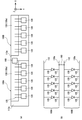
도 1은 본 발명의 제1 실시형태에 따른 광 조사 모듈(100)의 개략적인 구성을 설명하는 도면이다. 도 1(a)는 광 조사 모듈(100)의 평면도이며, 도 1(b)는 광 조사 모듈(100)의 측면도이며, 도 1(c)는 광 조사 모듈(100)의 등가 회로도이다. 본 실시형태의 광 조사 모듈(100)은, 자외광 조사장치 등에 탑재되어 자외광을 발하는 장치이다.1 is a view for explaining a schematic configuration of a
도 1에 도시한 바와 같이, 본 실시형태의 광 조사 모듈(100)은, 기판(110)과, 기판(110)의 표면에 재치(載置)된 복수(도 1에 있어서는 5개)의 LED 칩(120)과, 기판(110)의 표면에 LED 칩(120)을 따라 배치된 배선 기판(130), 및 기판(110)의 뒷면에 배치된 히트 싱크(150)를 구비하고 있다. 한편, 본 명세서에 있어서는, 광 조사 모듈(100)로부터 출사되는 자외광의 진행 방향을 Z축 방향이라 하고, LED 칩(120)의 배열 방향을 X축 방향이라 하고, X축 방향 및 Z축 방향과 직교하는 방향을 Y축 방향이라고 정의하여 설명한다.1, the
기판(110)은, 박판 형상의 메탈 베이스(112)와, 절연부(114)에 의해 구성된 2층 구조의 기판이다. 메탈 베이스(112)는, 도전성을 가지는 금속 재료(예를 들면, 구리, 알루미늄)로 이루어진 박판 형상(예를 들면, 두께 1.0∼2.0mm)의 부재이며, 표면에는 5개의 LED 칩(120)이 X축 방향을 따라 재치(載置)되어 있다. 본 실시형태의 메탈 베이스(112)는, 도시하지 않은 LED 구동회로와 전기적으로 접속되어 있어, LED 구동회로로부터 공급되는 전력을 LED 칩(120)의 애노드 단자(도시하지 않음)에 공급하는 기능을 가지고 있다.The
절연부(114)는, 절연성을 가지는 기재(예를 들면, 세라믹(질화 알루미늄, 알루미나, 질화 규소, 탄화 규소 등))로 이루어진 박판 형상의 부재이며, 메탈 베이스(112)의 뒷면측에 밀착된 상태에서, 접착 등에 의해 고정되어 있다. 상세한 것은 후술하지만, 본 실시형태의 절연부(114)는, 메탈 베이스(112)의 두께보다 얇게(예를 들면, 두께 100∼600μm) 구성되어 있다. 한편, 다른 실시형태로서는, 절연부(114)는, 메탈 베이스(112)의 뒷면에 도막을 형성하는 것에 의해 구성할 수도 있다.The insulating portion 114 is a thin plate-like member made of a substrate having an insulating property (for example, ceramic (aluminum nitride, alumina, silicon nitride, silicon carbide or the like) In the state of being fixed by adhesion or the like. The insulating section 114 of the present embodiment is configured to be thinner than the thickness of the metal base 112 (for example, 100 to 600 m in thickness), although the details will be described later. On the other hand, as another embodiment, the insulating portion 114 may be formed by forming a coating film on the back surface of the
도 1에 도시한 바와 같이, 본 실시형태에 있어서는, 5개의 LED 칩(120)이, Z축 방향으로 광축을 맞추고, X축 방향을 따라 근접 배치되어 있다. LED 칩(120)은, 예를 들면, 1.0mm(X축 방향길이) × 1.0mm(Y축 방향길이)의 평면에서 보았을 때 직사각형의 외형을 가지고(도 1(a)), 상면(즉, 출사면(120a))에 캐소드 단자(도시하지 않음)를 구비하고, 하면에 애노드 단자(도시하지 않음)를 구비하고 있다. 그리고, 애노드 단자와 캐소드 단자간에 전류가 인가되면, 발광층(도시하지 않음)에 있어서 자외광(예를 들면, 파장 385nm의 광)이 발생하고, 출사면(120a)으로부터 출사된다. 본 실시형태에 있어서는, LED 칩(120)은, 하면(즉, 애노드 단자)을 메탈 베이스(112)를 향하게 하여, 메탈 베이스(112) 상에 탑재되고, 다이 접착제(도시하지 않음)에 의해 메탈 베이스(112)에 접합되어 있다. 다이 접착제는, LED 칩(120)과 메탈 베이스(112)를 기계적 및 전기적으로 접합하기 위한 부재이며, 예를 들면, 도전성을 가지는 은(Ag) 페이스트가 이용되고 있다.As shown in Fig. 1, in the present embodiment, five
배선 기판(130)은, 표면에 배선 패턴(130a)이 형성된, 절연성을 가지는 기재(예를 들면, 글래스 에폭시 수지, 페이퍼 에폭시 수지, 세라믹스 등)로 이루어진 박판 형상의 부재이다. 배선 패턴(130a)은, 각 LED 칩(120)의 캐소드 단자에 전력을 공급하기 위한 공통의 메탈 패턴이며, 각 LED 칩(120)의 캐소드 단자와 한 쌍의 본딩 와이어(125)를 통해 접속되어 있다. 또한, 본 실시형태의 배선 기판(130)은, 도시하지 않은 LED 구동회로와 전기적으로 접속되어 있어, LED 구동회로로부터 공급되는 전력을 LED 칩(120)의 캐소드 단자에 공급하는 기능을 가지고 있다.The
히트 싱크(150)는, 복수의 방열 핀(150a)을 구비한 금속(예를 들면, 구리, 알루미늄)제의 방열부재이며, 예를 들면, 방열 그리스에 의해 절연부(114)의 뒷면에 밀착 고정되어 있다. 이처럼, 기판(110)의 뒷면에 히트 싱크(150)를 설치함으로써, 각 LED 칩(120)에 있어서 발생하는 열을 효율적으로 공기 중에 방열할 수 있다.The
전술한 바와 같이, 본 실시형태의 5개의 LED 칩(120)은, 애노드 단자가 메탈 베이스(112)에 접합되고, 캐소드 단자가 배선 패턴(130a)에 접속되어 있다. 따라서, 도 1(c)에 도시한 바와 같이, 5개의 LED 칩(120)은 병렬 접속되게 된다. LED 구동회로로부터 메탈 베이스(112) 및 배선 패턴(130a)에 전력이 공급되면, 5개의 LED 칩(120)이 발광하고, 광 조사 모듈(100)로부터는 X축 방향을 따라 연장되는 자외광이 출사된다.As described above, in the five
각 LED 칩(120)이 발광하면, 각 LED 칩(120)이 발열하는 문제가 있다. 이러한 발열 문제는, 본 실시형태와 같이 자외광을 발광하는 LED 칩(120)을 이용하는 경우, 공급하는 전력(예를 들면, 2.5W)의 약 2/3가 열로 전환된다는 점에서 특히 현저해진다고 할 수 있다.When each
그리하여, 이 점에 대해, 본원 발명자는 예의 검토를 실시했다. 그 결과, 종래, 글래스 에폭시 기판 등의 절연성 기판 상에 배치되어 있던 LED 칩을, 열 전도성이 좋은 금속제 기판 상에 직접 배치하고, 금속제 기판의 뒷면측에 절연층을 설치하는 구성으로 하면, LED 칩(120)의 열을 효율적으로 전도시킬 수 있지 않을까 하는 착상을 얻었다. 그리고, 본원 발명자는, 한층 더 예의 검토를 거듭하여, 금속제 기판의 두께 및 절연층의 두께를 최적화함으로써, 효율적인 냉각을 실시할 수 있다라는 의견에 도달했다.Thus, the present inventor has conducted intensive studies on this point. As a result, if the LED chip disposed on the insulating substrate such as the glass epoxy substrate is disposed directly on the metal substrate having good thermal conductivity and the insulating layer is provided on the rear surface side of the metal substrate, The heat of the
이하, 본원 발명자가 실시한 시뮬레이션을 설명하고, 금속제 기판(즉, 메탈 베이스(112))의 두께 및 절연층(즉, 절연부(114))의 두께의 조건에 관해 설명한다.The simulation performed by the present inventor will be described below and the conditions of the thickness of the metal substrate (that is, the metal base 112) and the thickness of the insulating layer (that is, the insulating portion 114) will be described.
표 1은, 상기한 본 실시형태의 광 조사 모듈(100)에 있어서, 메탈 베이스(112)와 절연부(114)의 두께를 변경하여, LED 칩(120)의 동작 온도를 시뮬레이션한 결과를 나타낸 표이다. 또한, 표 2는, 본 실시형태의 광 조사 모듈(100)에 대한 비교예를 나타낸 것으로서, LED 칩을 절연성 기판 상에 배치한 종래 구성에 있어서(즉, 본 실시형태의 메탈 베이스(112)와 절연부(114)의 배치를 반전시킨 구성에 있어서), 절연성 기판과 그 뒷면에 배치한 메탈 베이스의 두께를 변경하여, LED 칩의 동작 온도를 시뮬레이션한 결과를 나타낸 표이다.Table 1 shows the result of simulating the operating temperature of the
한편, 시뮬레이션 조건은 이하와 같다.The simulation conditions are as follows.
(1)LED: 1mm각(1) LED: 1mm square
(2)메탈 베이스 재질: 구리(2) Metal base material: Copper
(3)절연부(절연성 기판): 10W/mK품(3) Insulation part (Insulation board): 10W / mK Width
(4)투입 전력: 2.5W(4) Input power: 2.5W
(5)방열 그리스: 10W/mK품, 0.05mm 두께(5) Thermal grease: 10W / mK, 0.05mm thick
(6)히트 싱크: 알루미늄제 25mm각 핀형 히트 싱크(높이 25mm)(6) Heatsink: Aluminum 25mm each pin type heat sink (25mm in height)
(7)냉각 방식: 자연 공냉(LED 아래방향)(7) Cooling system: Natural air cooling (LED downward direction)
(8)외기온: 25℃(8) Outside temperature: 25 ℃
표 1과 표 2를 비교하면 알 수 있듯이, 메탈 베이스 및 절연부(절연성 기판)의 두께가 각각 동일하더라도, LED 칩(120)의 바로 아래에 메탈 베이스(112)를 배치하는 구성 (즉, 본 실시형태의 광 조사 모듈(100)의 구성)으로 하는 것이, LED 칩의 바로 아래에 절연부(절연성 기판)을 배치하는 구성(즉, 종래 구성)에 비해, LED 칩(120)의 동작 온도를 8∼9℃ 정도 낮출 수 있다는 것을 알 수 있다. 이것은, LED 칩(120)의 바로 아래에 배치되는 구성의 재료로부터 기인하며, 메탈 베이스(112)의 열 저항 쪽이, 절연부(절연성 기판)의 열 저항에 비교해서 작다 라는 것에 의한 것으로 짐작된다.As can be seen from the comparison between Table 1 and Table 2, even if the thicknesses of the metal base and the insulating portion (insulating substrate) are the same, the structure in which the
또한, 표 1로부터, 메탈 베이스(112)를 1.0mm에서 2.0mm까지 두껍게 하면, LED 칩(120)의 동작 온도를 0.6∼0.7℃ 정도 낮출 수 있다는 것을 알 수 있다. 또한, 절연부(114)를 600μm부터 100μm까지 얇게 하면, LED 칩(120)의 동작 온도를 1.3∼1.5℃ 정도 낮출 수 있다는 것을 알 수 있다. 그러나, 메탈 베이스(112)의 두께 조정 및 절연부(114)의 두께 조정에 의한 LED 칩(120)의 동작 온도의 저하량은, 메탈 베이스(112)와 절연부(114)의 배치 변경에 의한 효과와 비교해서 현격히 적다. 이러한 것으로부터, LED 칩(120)의 바로 아래에 메탈 베이스(112)를 배치하면, LED 칩(120)의 열이 메탈 베이스(112)내에서 순간적으로 확산되어 있는 것으로 추찰된다.It can be seen from Table 1 that the operating temperature of the
이상의 시뮬레이션 결과로부터, 본 실시형태에 있어서는, LED 칩(120)의 바로 아래에 메탈 베이스(112)를 배치하고, 그 두께를 1.0∼2.0mm의 범위로 설정하고 있다. 또한, LED 칩(120)의 바로 아래에 메탈 베이스(112)를 배치하면, LED 칩(120)에 대한 급전(給電) 필요성으로 인해, 메탈 베이스(112)에 대해 전력을 공급할 필요가 생긴다. 이를 위해, 본 실시형태에 있어서는, 메탈 베이스(112)로부터 각 LED 칩(120)으로의 전력 공급을 안정적이면서 확실히 실시하기 위해, 메탈 베이스(112)와 히트 싱크(150) 사이에 절연부(114)를 설치하고 있다. 한편, 절연부(114)의 두께에 대해서는, 본원 발명자의 다른 시뮬레이션에 의해, 메탈 베이스(112)의 두께보다 얇으면 충분히 효과가 있다는 것을 알 수 있으며, 바람직하게는 100∼600μm이다.From the above simulation results, in the present embodiment, the
또한, 본 실시형태의 광 조사 모듈(100)에 있어서는, X축 방향을 따라 복수의 광 조사 모듈(100)을 연결 가능하도록 구성되어 있다. 그리고, 본 실시형태의 광 조사 모듈(100)에는, 5개의 LED 칩(120)의 애노드 단자와 접합된 메탈 베이스(112)가, LED 칩(120)의 출사면(120a)와 같은 쪽에 노출되어 있기 때문에, 이것을 이용하여, 연결된 복수의 광 조사 모듈(100)을 전기적으로 접속하는 것이 가능하도록 되어 있다. 구체적으로는, 도 1에 도시한 바와 같이, 배선 기판(130)의 X축 방향의 길이가, 기판(110)의 X축 방향의 길이보다 짧으며, 배선 기판(130)의 외측(도 1(a), (b)에 있어서 좌측)의 메탈 베이스(112) 상에, 접합부(112a)(노출부)가 형성되어 있어, 이에 의해 연결된 복수의 광 조사 모듈(100)을 전기적으로 접속할 수 있도록 되어 있다.Further, in the
도 2는 2개의 광 조사 모듈(100A, 100B)을 연결한 구성을 나타낸 도면이다. 도 2(a)는 연결된 광 조사 모듈(100A, 100B)의 평면도이며, 도 2(c)는 연결된 광 조사 모듈(100A, 100B)의 등가 회로도이다. 한편, 도 2에 있어서는, 설명 편의상, 좌측의 광 조사 모듈(100)에 대해 「100A」의 부호를 붙이고, 우측의 광 조사 모듈(100)에 대해 「100B」의 부호를 붙였지만, 광 조사 모듈(100A) 및 광 조사 모듈(100B)의 구성은, 상술한 본 실시형태의 광 조사 모듈(100)과 완전히 동일하다.2 is a view showing a configuration in which two
도 2에 도시한 바와 같이, 광 조사 모듈(100A)과 광 조사 모듈(100B)은, X축 방향으로 연속하도록 밀착 배치되고, 도시하지 않은 지지부재로 연결하여 지지되어 있다. 그리고, 광 조사 모듈(100A)과 광 조사 모듈(100B)이 연결되었을 때, 광 조사 모듈(100A)의 배선 패턴(130a)과 광 조사 모듈(100B)의 접합부(112a)가 근접 배치되고, 이음매 부분에 접합부재(160)를 배치함으로써, 양자가 전기적으로 접속된다. 접합부재(160)는, 도전성을 가지는 금속(예를 들면, 구리, 알루미늄 등)으로 이루어진 가늘고 긴 부재이며, 일단부가 광 조사 모듈(100A)의 배선 패턴(130a)과 솔더링 등에 의해 접속되고, 타단부가 광 조사 모듈(100B)의 메탈 베이스(112)와 솔더링 등에 의해 접속되어 있다. 따라서, 도 2(c)에 도시한 바와 같이, 광 조사 모듈(100A)과 광 조사 모듈(100B)은, 접합부재(160)에 의해, 전기적으로는 직렬로 접속된다. 이처럼, 복수의 광 조사 모듈(100)을 직렬로 접속하면, 높은 LED 구동 전압이 필요해지지만, 소비 전류가 상승하는 일은 없다.As shown in Fig. 2, the
이처럼, 본 실시형태의 광 조사 모듈(100)은, X축 방향을 따라 용이하게 연결할 수 있도록 되어 있으며, 이에 의해, 원하는 라인 길이의 자외광을 용이하게 얻을 수 있도록 되어 있다. 한편, 본 실시형태에 있어서는, 광 조사 모듈(100)의 X축 방향 일단부측((도 1(a), (b)에 있어서 좌측)에 접합부(112a)를 설치하는 구성으로 했지만, Y축 방향 일단부측에 접합부(112a)를 설치할 수도 있으며, 이 경우, 광 조사 모듈(100)을 Y축 방향을 따라 연결하는 것이 가능해진다.As described above, the
이상이 본 발명의 실시형태의 설명이지만, 본 발명은, 상기 실시형태의 구성에 한정되지 않으며, 그 기술적 사상의 범위 내에서 여러 가지 변형이 가능하다.Although the embodiments of the present invention are described above, the present invention is not limited to the configurations of the above embodiments, and various modifications are possible within the scope of the technical idea.
예를 들면, 본 실시형태에 있어서는, 광 조사 모듈(100)이 5개의 LED 칩(120)을 구비하는 것으로 했지만, LED 칩(120)의 개수에 제한은 없으며, 광 조사 모듈(100)은, 적어도 2개의 LED 칩(120)을 구비하고 있으면 된다.For example, in the present embodiment, the
또한, 본 실시형태의 LED 칩(120)은, 자외광을 발하는 것으로서 설명했지만, 이러한 구성에 한정되지 않으며, 예를 들면, LED 칩(120)은, 가시영역 또는 적외영역의 광을 발하는 것일 수도 있다.Although the
(제2 실시형태)(Second Embodiment)
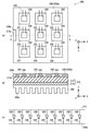
도 3은 본 발명의 제2 실시형태에 따른 광 조사 모듈(200)의 개략적인 구성을 설명하는 도면이다. 도 3(a)는 광 조사 모듈(200)의 평면도이며, 도 3(b)는 도 3(a)의 A-A 단면도이며, 도 3(c)는 광 조사 모듈(200)의 등가 회로도이다. 본 실시형태의 광 조사 모듈(200)은, LED 칩(220)이 기판(210) 상에 3개(X축 방향) × 3개(Y축 방향)의 형태로 2차원 매트릭스 형태로 배치되어 있다는 점에서, 제1 실시형태의 광 조사 모듈(100)과 상이하다.3 is a view for explaining a schematic configuration of the
도 3에 도시한 바와 같이, 본 실시형태의 광 조사 모듈(200)은, 기판(210)과, 기판(210)의 표면에 재치(載置)된 복수(도 2에 있어서는 9개)의 LED 칩(220)과, 기판(210)의 표면에 LED 칩(220)을 둘러싸도록 배치된 배선 기판(230), 및 기판(210)의 뒷면에 배치된 히트 싱크(250)를 구비하고 있다.3, the
기판(210)은, 제1 실시형태의 기판(110)과 동일한 기판이며, 박판 형상의 메탈 베이스(212)와, 절연부(214)에 의해 구성된 2층 구조의 기판이다. 메탈 베이스(212)의 표면에는 9개의 LED 칩(220)이, 3개(X축 방향) × 3개(Y축 방향)의 형태로 2차원 매트릭스 형태로 배치되어 있다.The
절연부(214)는, 제1 실시형태의 절연부(114)와 동일한 부재이며, 메탈 베이스(212)의 뒷면측에 밀착된 상태에서, 접착 등에 의해 고정되어 있다.The insulating
LED 칩(220)은, 제1 실시형태의 LED 칩(120)과 동일한 소자이며, 하면(즉, 애노드 단자)이 메탈 베이스(212)의 표면을 향하도록, 메탈 베이스(212) 상에 재치(載置)되고, 다이 접착제(도시하지 않음)에 의해 메탈 베이스(212)에 접합되어 있다.The
배선 기판(230)은, 절연성을 가지는 기재(예를 들면, 글래스 에폭시 수지, 페이퍼 에폭시 수지, 세라믹스 등)로 이루어진 박판 형상의 부재이다. 본 실시형태의 배선 기판(230)은, 9개의 LED 칩(220)을 각각 수용하는 9개의 개구부(231∼239)를 구비하고 있다. 배선 기판(230)은, 배선 기판(230)의 표면 전체를 덮도록 형성된 배선 패턴(230a)을 구비하고 있다. 배선 패턴(230a)은, 각 LED 칩(220)의 캐소드 단자에 전력을 공급하기 위한 공통의 메탈 패턴이며, 각 LED 칩(220)의 캐소드 단자와 한 쌍의 본딩 와이어(225)를 통해 접속되어 있다.The
히트 싱크(250)는, 복수의 방열 핀(250a)을 구비한, 제1 실시형태의 히트 싱크(150)와 동일한 부재이다.The
본 실시형태의 9개의 LED 칩(220)은, 애노드 단자가 메탈 베이스(212)에 접합되고, 캐소드 단자가 배선 패턴(230a)에 접속되어 있다. 따라서, 도 3(c)에 도시한 바와 같이, 9개의 LED 칩(120)은 병렬 접속되게 된다. 따라서, 도시하지 않은 LED 구동회로로부터 메탈 베이스(212) 및 배선 패턴(230a)에 전력이 공급되면, 9개의 LED 칩(220)이 발광하고, 광 조사 모듈(200)로부터는 X축 방향 및 Y축 방향을 따라 확산되는 자외광이 출사된다.In the nine
또한, 본 실시형태의 광 조사 모듈(200)에 있어서는, 배선 기판(230)의 일부에 절결부(230b)가 형성되어 있어, 메탈 베이스(212)의 일부가 LED 칩(120)의 출사면(120a)과 같은 측에 노출되고, 접합부(212a)(노출부)가 형성되어 있다. 이로 인해, 본 실시형태의 광 조사 모듈(200)에 있어서도, 본 실시형태의 광 조사 모듈(100)과 마찬가지로 복수의 광 조사 모듈(200)을 X축 방향으로 연결할 수 있다.In the
도 4는 2개의 광 조사 모듈(200A, 200B)을 연결한 구성을 나타낸 도면이다. 도 4(a)는 연결된 광 조사 모듈(200A, 200B)의 평면도이며, 도 4(c)는 연결된 광 조사 모듈(200A, 200B)의 등가 회로도이다. 한편, 도 4에 있어서는, 설명 편의상, 좌측의 광 조사 모듈(200)에 대해 「200A」의 부호를 붙이고, 우측의 광 조사 모듈(200)에 대해 「200B」의 부호를 붙였지만, 광 조사 모듈(200A) 및 광 조사 모듈(200B)의 구성은, 상술한 본 실시형태의 광 조사 모듈(200)과 완전히 동일하다.FIG. 4 is a view showing a configuration in which two
도 4에 도시한 바와 같이, 광 조사 모듈(200A)과 광 조사 모듈(200B)은, X축 방향으로 연속하도록 밀착 배치되고, 도시하지 않은 지지부재로 연결하여 지지되어 있다. 그리고, 광 조사 모듈(200A)과 광 조사 모듈(200B)이 연결되었을 때, 광 조사 모듈(200A)의 배선 패턴(230a)과 광 조사 모듈(200B)의 접합부(212a)가 근접 배치되고, 이음매 부분에 접합부재(260)를 배치함으로써, 양자가 전기적으로 접속된다. 접합부재(260)는, 제1 실시형태의 접합부재(160)와 동일하며, 일단부가 광 조사 모듈(200A)의 배선 패턴(230a)과 솔더링 등에 의해 접속되고, 타단부가 광 조사 모듈(200B)의 메탈 베이스(212)와 솔더링 등에 의해 접속되어 있다. 따라서, 도 4(b)에 도시한 바와 같이, 광 조사 모듈(200A)과 광 조사 모듈(200B)은, 접합부재(260)에 의해, 전기적으로는 직렬로 접속된다. 이처럼, 복수의 광 조사 모듈(200)을 직렬로 접속하면, 높은 LED 구동 전압이 필요해지지만, 소비 전류가 상승하는 일은 없다.As shown in Fig. 4, the
이처럼, 본 실시형태의 광 조사 모듈(200)도, 제1 실시형태의 광 조사 모듈(100)과 마찬가지로, X축 방향을 따라 용이하게 연결할 수 있도록 되어 있으며, 이에 의해, 원하는 라인 길이의 자외광을 용이하게 얻을 수 있도록 되어 있다. 한편, 본 실시형태에 있어서는, 광 조사 모듈(200)의 1변에 접합부재(260)를 설치하는 구성으로 했지만, X축 방향 및 Y축 방향에 따른 4변에 각각 접속부(230b)를 설치함으로써, 양방향으로 광 조사 모듈(200)을 연결하는 것이 가능해진다.Like the
(제3 실시형태)(Third Embodiment)
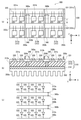
도 5는 본 발명의 제3 실시형태에 따른 광 조사 모듈(300)의 개략적인 구성을 설명하는 도면이다. 도 5(a)는 광 조사 모듈(300)의 평면도이며, 도 5(b)는 도 5(a)의 B-B 단면도이며, 도 5(c)는 광 조사 모듈(300)의 등가 회로도이다. 본 실시형태의 광 조사 모듈(300)은, 메탈 베이스(312)가 X축 방향을 따라 3개의 메탈 베이스(312a, 312b, 312c)로 분할되어 있다는 점에서, 제1 실시형태의 광 조사 모듈(100) 및 제2 실시형태의 광 조사 모듈(200)과 상이하다.5 is a view for explaining a schematic configuration of the
도 5에 도시한 바와 같이, 본 실시형태의 광 조사 모듈(300)은, 기판(310)과, 기판(310)의 표면에 재치(載置)된 복수(도 5에 있어서는 12개)의 LED 칩(320)과, 기판(310)의 표면에 LED 칩(320)을 따라 배치된 2장의 배선 기판(330), 및 기판(310)의 뒷면에 배치된 히트 싱크(350)를 구비하고 있다.5, the
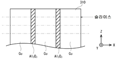
기판(310)은, 박판 형상의 메탈 베이스(312)와, 절연부(314)에 의해 구성된 2층 구조의 기판이다. 본 실시형태의 메탈 베이스(312)는, 절연부재(340)을 개재시켜, 3개의 메탈 베이스(312a, 312b, 312c)로 분할되어 있다. 절연부재(340)는, 예를 들면, 알루미나(Al2O3)이다. 이러한 구성의 메탈 베이스(312)는, 예를 들면, 도 6에 도시한 바와 같이, 3장의 동판(도 6중, 「Cu」로 나타낸 부재)과, 2장의 알루미나 기재(도 6중, 「Al2O3로 나타낸 부재)를 X축 방향으로 교대로 적층하여 접착하고, 적층방향(X축 방향)과 평행한 방향으로 슬라이스함으로써 얻어진다.The
절연부(314)는, 제1 실시형태의 절연부(114)와 동일한 부재이며, 메탈 베이스(312)의 뒷면측에 밀착된 상태에서, 접착 등에 의해 고정되어 있다.The insulating
LED 칩(320)은, 제1 실시형태의 LED 칩(120)과 동일한 소자이며, 하면(즉, 애노드 단자)이 메탈 베이스(312)의 표면을 향하도록, 메탈 베이스(312) 상에 재치(載置)되고, 다이 접착제(도시하지 않음)에 의해 메탈 베이스(312)에 접합되어 있다. 한편, 도 5(a)에 도시한 바와 같이, 본 실시형태의 LED 칩(320)은, 절연부재(340)와 배선 기판(330)으로 구획된 6개의 직사각형 영역의 각각에 2개씩 배치되어 있다.The
배선 기판(330)은, 절연성을 가지는 기재(예를 들면, 글래스 에폭시 수지, 페이퍼 에폭시 수지, 세라믹스 등)로 이루어진 박판 형상의 부재이다. 본 실시형태의 배선 기판(330)은, 도 5(a) 중, 상측의 6개의 LED 칩(320)과 접속되는 배선 기판(331), 및 하측의 6개의 LED 칩(320)과 접속되는 배선 기판(332)으로 구성되어 있다. 배선 기판(331)의 표면에는, 메탈 베이스(312a)에 배치된 2개의 LED 칩(320)의 캐소드 단자와 본딩 와이어(325)를 통해 접속되는 배선 패턴(331a)과, 메탈 베이스(312b)에 배치된 2개의 LED 칩(320)의 캐소드 단자와 본딩 와이어(325)를 통해 접속되는 배선 패턴(33lb), 및 메탈 베이스(312c)에 배치된 2개의 LED 칩(320)의 캐소드 단자와 본딩 와이어(325)를 통해 접속되는 배선 패턴(331c)이 형성되어 있다. 또한, 배선 기판(332)의 표면에는, 메탈 베이스(312a)에 배치된 2개의 LED 칩(320)의 캐소드 단자와 본딩 와이어(325)를 통해 접속되는 배선 패턴(332a)과, 메탈 베이스(312b)에 배치된 2개의 LED 칩(320)의 캐소드 단자와 본딩 와이어(325)를 통해 접속되는 배선 패턴(332b), 및 메탈 베이스(312c)에 배치된 2개의 LED 칩(320)의 캐소드 단자와 본딩 와이어(325)를 통해 접속되는 배선 패턴(332c)이 형성되어 있다.The
또한, 도 5(a), (b)에 도시한 바와 같이, 본 실시형태의 광 조사 모듈(300)은, 배선 기판(331), 및 배선 기판(332)을 걸쳐서 배치된 버스바(350a, 350b, 350c)를 구비하고 있다. 버스바(350a)는, 배선 패턴(331a)과 배선 패턴(332a)을 전기적으로 접속하는 부재이다. 버스바(350a)에 의해, 배선 패턴(331a)과 배선 패턴(332a)이 전기적으로 접속됨으로써, 메탈 베이스(312a) 상에 배치된 4개의 LED 칩(320)의 캐소드 단자가 전기적으로 접속된다. 버스바(350b)는, 배선 패턴(33lb)과 배선 패턴(332b)을 전기적으로 접속하는 부재이다. 버스바(350b)에 의해, 배선 패턴(33lb)과 배선 패턴(332b)이 전기적으로 접속됨으로써, 메탈 베이스(312b) 상에 배치된 4개의 LED 칩(320)의 캐소드 단자가 전기적으로 접속된다. 버스바(350c)는, 배선 패턴(331c)과 배선 패턴(332c)을 전기적으로 접속하는 부재이다. 버스바(350c)에 의해, 배선 패턴(331c)과 배선 패턴(332c)이 전기적으로 접속됨으로써, 메탈 베이스(312c) 상에 배치된 4개의 LED 칩(320)의 캐소드 단자가 전기적으로 접속된다.5A and 5B, the
또한, 본 실시형태의 버스바(350a)는, 와이어(360a)에 의해, 메탈 베이스(312b)에 접속되어 있다. 또한, 본 실시형태의 버스바(350b)는, 와이어(360b)에 의해, 메탈 베이스(312c)에 접속되어 있다.The
이처럼, 본 실시형태의 12개의 LED 칩(320)은, 3개의 메탈 베이스(312a, 312b, 312c)에 의해, X축 방향으로 3개의 그룹으로 나뉘어져 있다. 그리고, 메탈 베이스(312a) 상의 4개의 LED 칩(320)의 캐소드 단자가 배선 패턴(331a), 배선 패턴(332a) 및 버스바(350a)에 의해 접속되기 때문에, 이들 4개의 LED 칩(320)은 병렬로 접속된다(도 5(c)). 또한, 메탈 베이스(312b) 상의 4개의 LED 칩(320)의 캐소드 단자가 배선 패턴(33lb), 배선 패턴(332b) 및 버스바(350b)에 의해 접속되기 때문에, 이들 4개의 LED 칩(320)은 병렬로 접속된다(도 5(c)). 또한, 메탈 베이스(312c) 상의 4개의 LED 칩(320)의 캐소드 단자가 배선 패턴(331c), 배선 패턴(332c) 및 버스바(350c)에 의해 접속되기 때문에, 이들 4개의 LED 칩(320)은 병렬로 접속된다(도 5(c)). 또한, 와이어(360a)에 의해, 버스바(350a)와 메탈 베이스(312b)가 접속되고, 와이어(360b)에 의해, 버스바(350b)와 메탈 베이스(312c)가 접속되기 때문에, 각 메탈 베이스(312a, 312b, 312c)의 4개의 LED 칩(320)은, 도 5(c)에 도시한 바와 같이 직렬 접속이 된다.As described above, the twelve
이처럼, 본 실시형태에 있어서는, 메탈 베이스(312)를 X축 방향으로 분할함으로써, 병렬 접속되는 LED 칩(320)을 그룹화하고, 그룹화한 각 LED 칩(320)을 직렬로 접속하고 있다. 도 6에 도시한 바와 같이, 메탈 베이스(312)의 분할수는 동판과, 알루미나 기재의 적층 매수로 결정되기 때문에, 적층 매수를 조정함으로써, 1장의 기판(310) 상에서, 직렬 접속되는 LED 칩(320)의 단수를 자유롭게 설정할 수 있다. 즉, 본 실시형태의 구성에 의하면, 제1 실시형태의 광 조사 모듈(100)이나 제2 실시형태의 광 조사 모듈(200)과 같이, 복수의 광 조사 모듈을 연결하지 않고, LED 칩(320)을 직렬로 접속하는 것이 가능해진다.As described above, in this embodiment, the
한편, 본 실시형태에 있어서는, 12개의 LED 칩(320)이, Y축 방향을 따라 2열로 나뉘어져 배치되어 있지만, 이러한 구성에 한정되지 않으며, 복수의 LED 칩(320)이, N열(N은 1 이상의 정수)로 나란히 배치되어 있을 수도 있다.In the present embodiment, the twelve
또한, 이번에 개시된 실시형태는, 모든 점에서 예시에 불과하며, 제한적인 것은 아니다. 본 발명의 범위는, 상기한 설명이 아니라, 특허 청구 범위에 의해 나타내어지며, 특허 청구 범위와 균등한 의미 및 범위 내에서의 모든 변경이 포함된다.Moreover, the embodiments disclosed herein are by way of example only in all respects, and are not restrictive. The scope of the present invention is defined by the appended claims rather than by the foregoing description, and includes all changes within the meaning and scope equivalent to the claims.
100, 200, 300: 광 조사 모듈
110, 210, 310: 기판
112, 212, 312, 312a, 312b, 312c: 메탈 베이스
112a, 212a: 접합부
114, 214, 314: 절연부
120, 220, 320: LED 칩
120a: 출사면
125, 225, 325: 본딩 와이어
130, 230, 330, 331, 332: 배선 기판
130a, 230a: 배선 패턴
150, 250: 히트 싱크
150a, 250a: 방열 핀
160: 접합부재
231, 232, 233, 234, 235, 236, 237, 238, 239: 개구부
350a, 350b: 버스바
360a, 360b: 와이어100, 200, 300: light irradiation module
110, 210 and 310:
112, 212, 312, 312a, 312b, 312c: metal base
112a, 212a:
114, 214, 314:
120, 220, 320: LED chip
120a: exit surface
125, 225, 325: bonding wire
130, 230, 330, 331, 332:
130a, 230a: wiring pattern
150, 250: Heat sink
150a, 250a:
160:
231, 232, 233, 234, 235, 236, 237, 238, 239:
350a, 350b: bus bar
360a, 360b: wire
Claims (12)
상기 기판은,
표면에 상기 복수의 LED 칩이 재치(載置)되고, 상기LED 칩의 뒷면에 형성된 제1 전극과 전기적으로 접속되어, 상기 제1 전극에 전력을 공급하는 판 형상의 메탈 베이스, 및
상기 메탈 베이스의 뒷면측에 밀착 설치된 절연부,
를 가지고,
상기 메탈 베이스 상에는, 상기 각 LED 칩의 표면에 형성된 제2 전극과 전기적으로 접속되어, 상기 제2 전극에 전력을 공급하는 배선 기판이 배치되고,
상기 메탈 베이스의 두께는 1.0∼2.0mm이며,
상기 절연부의 두께가, 상기 메탈 베이스의 두께보다 얇은 것을 특징으로 하는 광 조사 모듈.
A plurality of LEDs (Light Emitting Diode) chips mounted on a surface of the substrate and emitting ultraviolet light in a direction orthogonal to the surface of the substrate, A light irradiation module comprising a heat dissipating member for dissipating heat generated in an LED chip to the outside,
Wherein:
A plate-shaped metal base on which the plurality of LED chips are mounted, a plate-shaped metal base electrically connected to a first electrode formed on a rear surface of the LED chip and supplying power to the first electrode,
An insulating portion provided closely to a rear surface side of the metal base,
Lt; / RTI &
A wiring board electrically connected to a second electrode formed on a surface of each of the LED chips and supplying power to the second electrode is disposed on the metal base,
The thickness of the metal base is 1.0 to 2.0 mm,
And the thickness of the insulating portion is thinner than the thickness of the metal base.
상기 절연부의 두께가 100∼600μm인 것을 특징으로 하는 광 조사 모듈.
The method according to claim 1,
Wherein the thickness of the insulating portion is 100 to 600 占 퐉.
상기 복수의 LED 칩이 병렬 접속되어 있는 것을 특징으로 하는 광 조사 모듈.
3. The method according to claim 1 or 2,
And the plurality of LED chips are connected in parallel.
상기 기판은, 평면에서 보았을 때 직사각형이며,
상기 복수의 LED 칩이, 상기 기판의 평행한 2변을 따라 일렬로 나란히 배치되어 있는 것을 특징으로 하는 광 조사 모듈.
4. The method according to any one of claims 1 to 3,
Wherein the substrate is rectangular when viewed in plan,
Wherein the plurality of LED chips are arranged in a line along two parallel sides of the substrate.
복수의 광 조사 모듈을 상기 복수의 LED 칩의 배열 방향으로 연결 가능하도록 구성 되어 있는 것을 특징으로 하는 광 조사 모듈.
5. The method of claim 4,
And the plurality of light irradiation modules are connectable in the arrangement direction of the plurality of LED chips.
상기 메탈 베이스는, 상기 복수의 LED 칩의 배열 방향의 일단부에 있어서, 표면이 노출되는 노출부를 가지고,
복수의 광 조사 모듈을 연결했을 때, 인접하는 한쪽의 광 조사 모듈의 배선 기판과 다른 광 조사 모듈의 노출부가 근접 배치되고, 상기 배선 기판과 상기 노출부가 전기적으로 접속되어 있는 것을 특징으로 하는 광 조사 모듈.
6. The method of claim 5,
Wherein the metal base has an exposed portion at one end of the array direction of the plurality of LED chips,
Wherein when the plurality of light irradiation modules are connected, the wiring substrate of the adjacent one of the light irradiation modules and the exposed portion of the other light irradiation module are arranged close to each other, and the wiring substrate and the exposed portion are electrically connected. module.
상기 기판은, 평면에서 보았을 때 직사각형이며,
상기 복수의 LED 칩이, 상기 기판 상에 2차원 매트릭스 형태로 배치되어 있는 것을 특징으로 하는 광 조사 모듈.
4. The method according to any one of claims 1 to 3,
Wherein the substrate is rectangular when viewed in plan,
Wherein the plurality of LED chips are arranged in a two-dimensional matrix on the substrate.
상기 배선 기판이, 상기 각 LED 칩의 주위를 둘러싸도록 배치되어 있는 것을 특징으로 하는 광 조사 모듈.
8. The method of claim 7,
Wherein the wiring board is arranged so as to surround the periphery of each of the LED chips.
복수의 광 조사 모듈을 상기 복수의 LED 칩의 한쪽의 배열 방향으로 연결 가능하도록 구성되어 있는 것을 특징으로 하는 광 조사 모듈.
9. The method of claim 8,
And the plurality of light irradiation modules are connectable in an arrangement direction of one of the plurality of LED chips.
상기 메탈 베이스는, 상기 복수의 LED 칩의 한쪽의 배열 방향의 일단부에 있어서, 표면이 노출되는 노출부를 가지고,
복수의 광 조사 모듈을 연결했을 때, 인접하는 한쪽의 광 조사 모듈의 배선 기판과 다른 광 조사 모듈의 노출부가 근접 배치되고, 상기 배선 기판과 상기 노출부가 전기적으로 접속되어 있는 것을 특징으로 하는 광 조사 모듈.
10. The method of claim 9,
Wherein the metal base has an exposed portion exposed at one end of one end of the array direction of the plurality of LED chips,
Wherein when the plurality of light irradiation modules are connected, the wiring substrate of the adjacent one of the light irradiation modules and the exposed portion of the other light irradiation module are arranged close to each other, and the wiring substrate and the exposed portion are electrically connected. module.
상기 기판은, 평면에서 보았을 때 직사각형이며,
상기 복수의 LED 칩이, 상기 기판의 평행한 2변을 따라 N열(N은 1 이상의 정수)로 나란히 배치되고,
상기 메탈 베이스는, 상기 복수의 LED 칩의 배열 방향과 직교하는 방향으로 복수로 분할되어 있으며,
상기 배선 기판은, 분할된 각 메탈 베이스 상에 재치(載置)되어 있는 상기 각 LED 칩을 1그룹으로 하여, 그룹마다 상기 제2 전극을 전기적으로 접속하고,
인접하는 한쪽의 메탈 베이스 상의 배선 기판과 다른 메탈 베이스가 전기적으로 접속되어 있는 것을 특징으로 하는 광 조사 모듈.
4. The method according to any one of claims 1 to 3,
Wherein the substrate is rectangular when viewed in plan,
Wherein the plurality of LED chips are arranged in parallel in N rows (N is an integer of 1 or more) side by side along two parallel sides of the substrate,
Wherein the metal base is divided into a plurality of portions in a direction orthogonal to an arrangement direction of the plurality of LED chips,
Wherein the wiring board comprises a plurality of LED chips mounted on each of the divided metal bases as a group and electrically connecting the second electrodes for each group,
Wherein the wiring substrate on one adjacent metal base and another metal base are electrically connected to each other.
상기 분할된 각 메탈 베이스간에 절연부재를 구비하는 것을 특징으로 하는 광 조사 모듈.
12. The method of claim 11,
And an insulating member between each of the divided metal bases.
Applications Claiming Priority (2)
| Application Number | Priority Date | Filing Date | Title |
|---|---|---|---|
| JP2015074298A JP2016195177A (en) | 2015-03-31 | 2015-03-31 | Light irradiation module |
| JPJP-P-2015-074298 | 2015-03-31 |
Publications (1)
| Publication Number | Publication Date |
|---|---|
| KR20160117260A true KR20160117260A (en) | 2016-10-10 |
Family
ID=57081398
Family Applications (1)
| Application Number | Title | Priority Date | Filing Date |
|---|---|---|---|
| KR1020160037006A KR20160117260A (en) | 2015-03-31 | 2016-03-28 | Light Irradiation Module |
Country Status (4)
| Country | Link |
|---|---|
| JP (1) | JP2016195177A (en) |
| KR (1) | KR20160117260A (en) |
| CN (1) | CN106024803A (en) |
| TW (1) | TW201636535A (en) |
Cited By (1)
| Publication number | Priority date | Publication date | Assignee | Title |
|---|---|---|---|---|
| KR20220033222A (en) * | 2020-09-09 | 2022-03-16 | (주)진영에이치앤에스 | A UVC LED Assembly |
Families Citing this family (1)
| Publication number | Priority date | Publication date | Assignee | Title |
|---|---|---|---|---|
| KR102650608B1 (en) * | 2020-12-18 | 2024-03-25 | 세메스 주식회사 | Light processing member, substrate processing apparatus including the same and substrate processing method |
Citations (1)
| Publication number | Priority date | Publication date | Assignee | Title |
|---|---|---|---|---|
| JP5582967B2 (en) | 2010-10-27 | 2014-09-03 | 京セラ株式会社 | Light irradiation apparatus, light irradiation module, and printing apparatus |
Family Cites Families (13)
| Publication number | Priority date | Publication date | Assignee | Title |
|---|---|---|---|---|
| JPS62196878A (en) * | 1986-02-25 | 1987-08-31 | Koito Mfg Co Ltd | Illumination system |
| JPS62229987A (en) * | 1986-03-31 | 1987-10-08 | Koito Mfg Co Ltd | Illuminator |
| JPH11298048A (en) * | 1998-04-15 | 1999-10-29 | Matsushita Electric Works Ltd | Led mounting board |
| JP4432275B2 (en) * | 2000-07-13 | 2010-03-17 | パナソニック電工株式会社 | Light source device |
| JP2007180320A (en) * | 2005-12-28 | 2007-07-12 | Matsushita Electric Ind Co Ltd | Light-emitting module and manufacturing method thereof |
| CN101076223A (en) * | 2006-09-26 | 2007-11-21 | 蔡勇 | Metal circuit board of aluminum baseplate magnetic-controlled sputtering-jetted and LED illuminating device |
| US20080099772A1 (en) * | 2006-10-30 | 2008-05-01 | Geoffrey Wen-Tai Shuy | Light emitting diode matrix |
| JP5330889B2 (en) * | 2009-04-14 | 2013-10-30 | 電気化学工業株式会社 | LED module for lighting |
| JP5526876B2 (en) * | 2010-03-09 | 2014-06-18 | 東京エレクトロン株式会社 | Heating device and annealing device |
| JP2012033742A (en) * | 2010-07-30 | 2012-02-16 | Nk Works Kk | Light irradiation device and printer using light-emitting diode |
| JP2015038902A (en) * | 2010-10-28 | 2015-02-26 | 国立大学法人九州工業大学 | Led module device and manufacturing method of the same |
| JP2013089769A (en) * | 2011-10-18 | 2013-05-13 | Koito Mfg Co Ltd | Light emitting module |
| JP2013239673A (en) * | 2012-05-17 | 2013-11-28 | Stanley Electric Co Ltd | Light emitting device and lamp for vehicle |
-
2015
- 2015-03-31 JP JP2015074298A patent/JP2016195177A/en active Pending
-
2016
- 2016-03-25 CN CN201610180618.XA patent/CN106024803A/en active Pending
- 2016-03-25 TW TW105109593A patent/TW201636535A/en unknown
- 2016-03-28 KR KR1020160037006A patent/KR20160117260A/en unknown
Patent Citations (1)
| Publication number | Priority date | Publication date | Assignee | Title |
|---|---|---|---|---|
| JP5582967B2 (en) | 2010-10-27 | 2014-09-03 | 京セラ株式会社 | Light irradiation apparatus, light irradiation module, and printing apparatus |
Cited By (1)
| Publication number | Priority date | Publication date | Assignee | Title |
|---|---|---|---|---|
| KR20220033222A (en) * | 2020-09-09 | 2022-03-16 | (주)진영에이치앤에스 | A UVC LED Assembly |
Also Published As
| Publication number | Publication date |
|---|---|
| TW201636535A (en) | 2016-10-16 |
| JP2016195177A (en) | 2016-11-17 |
| CN106024803A (en) | 2016-10-12 |
Similar Documents
| Publication | Publication Date | Title |
|---|---|---|
| US7439549B2 (en) | LED module | |
| US9434151B2 (en) | LED unit | |
| JP4241658B2 (en) | Light emitting diode light source unit and light emitting diode light source formed using the same | |
| US8622578B2 (en) | Flexible LED array | |
| EP1895602B1 (en) | Illumination apparatus having a plurality of semiconductor light-emitting devices | |
| EP2565951B1 (en) | Light emitting unit and illuminating apparatus | |
| US7897980B2 (en) | Expandable LED array interconnect | |
| US8847251B2 (en) | Substrate, light-emitting device, and lighting apparatus having a largest gap between two lines at light-emitting element mounting position | |
| KR102204216B1 (en) | Supports and lighting devices for light-emitting elements | |
| JP2005158957A (en) | Light emitting device | |
| TWI436509B (en) | Led module | |
| KR20160117260A (en) | Light Irradiation Module | |
| WO2020121961A1 (en) | Circuit board and vehicle light | |
| US7868347B2 (en) | Metal core multi-LED SMD package and method of producing the same | |
| JP7007569B2 (en) | Luminescent device | |
| JP2022031370A (en) | Light-emitting device and light-emitting module | |
| JP4862808B2 (en) | Light emitting device | |
| KR20180073288A (en) | Printed circuit board for light emitting diode arrangement with enhanced heat releasing efficiency | |
| KR20130007473A (en) | Led pcb substrate, pcb, led unit, lighting and its manufacture | |
| KR20180073292A (en) | Printed circuit board for light emitting diode arrangement with enhanced heat releasing efficiency | |
| KR200456702Y1 (en) | LED mount structure for the shear plane of PWB or material of radiant heat. | |
| JP2023008051A (en) | Ultraviolet irradiation device and exposure device | |
| JP2016066693A (en) | Light-emitting module |