KR20140135184A - 배면측-조명 센서들을 제조하기 위한 방법 - Google Patents
배면측-조명 센서들을 제조하기 위한 방법 Download PDFInfo
- Publication number
- KR20140135184A KR20140135184A KR1020147025054A KR20147025054A KR20140135184A KR 20140135184 A KR20140135184 A KR 20140135184A KR 1020147025054 A KR1020147025054 A KR 1020147025054A KR 20147025054 A KR20147025054 A KR 20147025054A KR 20140135184 A KR20140135184 A KR 20140135184A
- Authority
- KR
- South Korea
- Prior art keywords
- backside
- semiconductor
- thin plate
- light sensor
- thickness
- Prior art date
- Legal status (The legal status is an assumption and is not a legal conclusion. Google has not performed a legal analysis and makes no representation as to the accuracy of the status listed.)
- Withdrawn
Links
- 238000000034 method Methods 0.000 title claims abstract description 52
- 239000004065 semiconductor Substances 0.000 claims abstract description 104
- 238000004519 manufacturing process Methods 0.000 claims abstract description 37
- 238000005286 illumination Methods 0.000 claims abstract description 11
- 239000011888 foil Substances 0.000 claims description 20
- 150000002500 ions Chemical class 0.000 claims description 18
- 239000010409 thin film Substances 0.000 claims description 17
- 239000000758 substrate Substances 0.000 claims description 16
- 238000001465 metallisation Methods 0.000 claims description 11
- 229910021417 amorphous silicon Inorganic materials 0.000 claims description 5
- 239000007943 implant Substances 0.000 claims description 4
- 238000004140 cleaning Methods 0.000 claims description 2
- 230000000295 complement effect Effects 0.000 claims description 2
- 238000000151 deposition Methods 0.000 claims description 2
- 229910044991 metal oxide Inorganic materials 0.000 claims description 2
- 150000004706 metal oxides Chemical class 0.000 claims description 2
- 238000002161 passivation Methods 0.000 claims description 2
- 230000008878 coupling Effects 0.000 claims 4
- 238000010168 coupling process Methods 0.000 claims 4
- 238000005859 coupling reaction Methods 0.000 claims 4
- 238000002347 injection Methods 0.000 claims 1
- 239000007924 injection Substances 0.000 claims 1
- 235000012431 wafers Nutrition 0.000 description 27
- XUIMIQQOPSSXEZ-UHFFFAOYSA-N Silicon Chemical compound [Si] XUIMIQQOPSSXEZ-UHFFFAOYSA-N 0.000 description 12
- 229910052710 silicon Inorganic materials 0.000 description 12
- 239000010703 silicon Substances 0.000 description 12
- 239000002019 doping agent Substances 0.000 description 10
- 239000000463 material Substances 0.000 description 9
- 239000011521 glass Substances 0.000 description 8
- ZOXJGFHDIHLPTG-UHFFFAOYSA-N Boron Chemical compound [B] ZOXJGFHDIHLPTG-UHFFFAOYSA-N 0.000 description 4
- KRHYYFGTRYWZRS-UHFFFAOYSA-N Fluorane Chemical compound F KRHYYFGTRYWZRS-UHFFFAOYSA-N 0.000 description 4
- 229910052796 boron Inorganic materials 0.000 description 4
- 238000009792 diffusion process Methods 0.000 description 4
- 238000005530 etching Methods 0.000 description 4
- 239000007789 gas Substances 0.000 description 4
- 229910052751 metal Inorganic materials 0.000 description 4
- 239000002184 metal Substances 0.000 description 4
- 229910021421 monocrystalline silicon Inorganic materials 0.000 description 4
- 239000005360 phosphosilicate glass Substances 0.000 description 4
- 238000000576 coating method Methods 0.000 description 3
- 238000000227 grinding Methods 0.000 description 3
- 229910052738 indium Inorganic materials 0.000 description 3
- APFVFJFRJDLVQX-UHFFFAOYSA-N indium atom Chemical compound [In] APFVFJFRJDLVQX-UHFFFAOYSA-N 0.000 description 3
- RYGMFSIKBFXOCR-UHFFFAOYSA-N Copper Chemical compound [Cu] RYGMFSIKBFXOCR-UHFFFAOYSA-N 0.000 description 2
- ATJFFYVFTNAWJD-UHFFFAOYSA-N Tin Chemical compound [Sn] ATJFFYVFTNAWJD-UHFFFAOYSA-N 0.000 description 2
- 238000000137 annealing Methods 0.000 description 2
- 125000004429 atom Chemical group 0.000 description 2
- 238000003776 cleavage reaction Methods 0.000 description 2
- 238000007906 compression Methods 0.000 description 2
- 238000011109 contamination Methods 0.000 description 2
- 229910052802 copper Inorganic materials 0.000 description 2
- 239000010949 copper Substances 0.000 description 2
- 230000007547 defect Effects 0.000 description 2
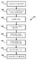
- 238000010586 diagram Methods 0.000 description 2
- 230000005684 electric field Effects 0.000 description 2
- 229910052734 helium Inorganic materials 0.000 description 2
- 239000001307 helium Substances 0.000 description 2
- 239000001257 hydrogen Substances 0.000 description 2
- 229910052739 hydrogen Inorganic materials 0.000 description 2
- 238000012986 modification Methods 0.000 description 2
- 230000004048 modification Effects 0.000 description 2
- QPJSUIGXIBEQAC-UHFFFAOYSA-N n-(2,4-dichloro-5-propan-2-yloxyphenyl)acetamide Chemical compound CC(C)OC1=CC(NC(C)=O)=C(Cl)C=C1Cl QPJSUIGXIBEQAC-UHFFFAOYSA-N 0.000 description 2
- RLOWWWKZYUNIDI-UHFFFAOYSA-N phosphinic chloride Chemical compound ClP=O RLOWWWKZYUNIDI-UHFFFAOYSA-N 0.000 description 2
- 238000005498 polishing Methods 0.000 description 2
- 238000000926 separation method Methods 0.000 description 2
- 239000000126 substance Substances 0.000 description 2
- 229910052718 tin Inorganic materials 0.000 description 2
- 229910001218 Gallium arsenide Inorganic materials 0.000 description 1
- UFHFLCQGNIYNRP-UHFFFAOYSA-N Hydrogen Chemical compound [H][H] UFHFLCQGNIYNRP-UHFFFAOYSA-N 0.000 description 1
- 241000446313 Lamella Species 0.000 description 1
- OAICVXFJPJFONN-UHFFFAOYSA-N Phosphorus Chemical compound [P] OAICVXFJPJFONN-UHFFFAOYSA-N 0.000 description 1
- 229910000577 Silicon-germanium Inorganic materials 0.000 description 1
- RTAQQCXQSZGOHL-UHFFFAOYSA-N Titanium Chemical compound [Ti] RTAQQCXQSZGOHL-UHFFFAOYSA-N 0.000 description 1
- LEVVHYCKPQWKOP-UHFFFAOYSA-N [Si].[Ge] Chemical compound [Si].[Ge] LEVVHYCKPQWKOP-UHFFFAOYSA-N 0.000 description 1
- 238000001505 atmospheric-pressure chemical vapour deposition Methods 0.000 description 1
- 238000006243 chemical reaction Methods 0.000 description 1
- 150000001875 compounds Chemical class 0.000 description 1
- 239000004020 conductor Substances 0.000 description 1
- HVMJUDPAXRRVQO-UHFFFAOYSA-N copper indium Chemical compound [Cu].[In] HVMJUDPAXRRVQO-UHFFFAOYSA-N 0.000 description 1
- KUNSUQLRTQLHQQ-UHFFFAOYSA-N copper tin Chemical compound [Cu].[Sn] KUNSUQLRTQLHQQ-UHFFFAOYSA-N 0.000 description 1
- 239000013078 crystal Substances 0.000 description 1
- 238000005520 cutting process Methods 0.000 description 1
- 230000032798 delamination Effects 0.000 description 1
- 230000008021 deposition Effects 0.000 description 1
- ALKZAGKDWUSJED-UHFFFAOYSA-N dinuclear copper ion Chemical compound [Cu].[Cu] ALKZAGKDWUSJED-UHFFFAOYSA-N 0.000 description 1
- 238000004299 exfoliation Methods 0.000 description 1
- 229910052732 germanium Inorganic materials 0.000 description 1
- GNPVGFCGXDBREM-UHFFFAOYSA-N germanium atom Chemical compound [Ge] GNPVGFCGXDBREM-UHFFFAOYSA-N 0.000 description 1
- SWQJXJOGLNCZEY-UHFFFAOYSA-N helium atom Chemical class [He] SWQJXJOGLNCZEY-UHFFFAOYSA-N 0.000 description 1
- -1 helium ions Chemical class 0.000 description 1
- 125000004435 hydrogen atom Chemical class [H]* 0.000 description 1
- 238000002513 implantation Methods 0.000 description 1
- RHZWSUVWRRXEJF-UHFFFAOYSA-N indium tin Chemical compound [In].[Sn] RHZWSUVWRRXEJF-UHFFFAOYSA-N 0.000 description 1
- 230000003993 interaction Effects 0.000 description 1
- 238000005468 ion implantation Methods 0.000 description 1
- 239000007788 liquid Substances 0.000 description 1
- 230000035515 penetration Effects 0.000 description 1
- 229910052698 phosphorus Inorganic materials 0.000 description 1
- 239000011574 phosphorus Substances 0.000 description 1
- 238000005240 physical vapour deposition Methods 0.000 description 1
- 238000009832 plasma treatment Methods 0.000 description 1
- 238000000623 plasma-assisted chemical vapour deposition Methods 0.000 description 1
- 238000002360 preparation method Methods 0.000 description 1
- 230000007017 scission Effects 0.000 description 1
- 238000007650 screen-printing Methods 0.000 description 1
- 229910000679 solder Inorganic materials 0.000 description 1
- 239000007787 solid Substances 0.000 description 1
- 241000894007 species Species 0.000 description 1
- 238000004544 sputter deposition Methods 0.000 description 1
- 239000010936 titanium Substances 0.000 description 1
- 229910052719 titanium Inorganic materials 0.000 description 1
- MAKDTFFYCIMFQP-UHFFFAOYSA-N titanium tungsten Chemical compound [Ti].[W] MAKDTFFYCIMFQP-UHFFFAOYSA-N 0.000 description 1
- 239000002699 waste material Substances 0.000 description 1
Images


Classifications
-
- H—ELECTRICITY
- H01—ELECTRIC ELEMENTS
- H01L—SEMICONDUCTOR DEVICES NOT COVERED BY CLASS H10
- H01L21/00—Processes or apparatus adapted for the manufacture or treatment of semiconductor or solid state devices or of parts thereof
- H01L21/67—Apparatus specially adapted for handling semiconductor or electric solid state devices during manufacture or treatment thereof; Apparatus specially adapted for handling wafers during manufacture or treatment of semiconductor or electric solid state devices or components ; Apparatus not specifically provided for elsewhere
- H01L21/683—Apparatus specially adapted for handling semiconductor or electric solid state devices during manufacture or treatment thereof; Apparatus specially adapted for handling wafers during manufacture or treatment of semiconductor or electric solid state devices or components ; Apparatus not specifically provided for elsewhere for supporting or gripping
- H01L21/6835—Apparatus specially adapted for handling semiconductor or electric solid state devices during manufacture or treatment thereof; Apparatus specially adapted for handling wafers during manufacture or treatment of semiconductor or electric solid state devices or components ; Apparatus not specifically provided for elsewhere for supporting or gripping using temporarily an auxiliary support
-
- H—ELECTRICITY
- H10—SEMICONDUCTOR DEVICES; ELECTRIC SOLID-STATE DEVICES NOT OTHERWISE PROVIDED FOR
- H10F—INORGANIC SEMICONDUCTOR DEVICES SENSITIVE TO INFRARED RADIATION, LIGHT, ELECTROMAGNETIC RADIATION OF SHORTER WAVELENGTH OR CORPUSCULAR RADIATION
- H10F30/00—Individual radiation-sensitive semiconductor devices in which radiation controls the flow of current through the devices, e.g. photodetectors
- H10F30/20—Individual radiation-sensitive semiconductor devices in which radiation controls the flow of current through the devices, e.g. photodetectors the devices having potential barriers, e.g. phototransistors
- H10F30/21—Individual radiation-sensitive semiconductor devices in which radiation controls the flow of current through the devices, e.g. photodetectors the devices having potential barriers, e.g. phototransistors the devices being sensitive to infrared, visible or ultraviolet radiation
- H10F30/22—Individual radiation-sensitive semiconductor devices in which radiation controls the flow of current through the devices, e.g. photodetectors the devices having potential barriers, e.g. phototransistors the devices being sensitive to infrared, visible or ultraviolet radiation the devices having only one potential barrier, e.g. photodiodes
- H10F30/221—Individual radiation-sensitive semiconductor devices in which radiation controls the flow of current through the devices, e.g. photodetectors the devices having potential barriers, e.g. phototransistors the devices being sensitive to infrared, visible or ultraviolet radiation the devices having only one potential barrier, e.g. photodiodes the potential barrier being a PN homojunction
-
- H—ELECTRICITY
- H10—SEMICONDUCTOR DEVICES; ELECTRIC SOLID-STATE DEVICES NOT OTHERWISE PROVIDED FOR
- H10F—INORGANIC SEMICONDUCTOR DEVICES SENSITIVE TO INFRARED RADIATION, LIGHT, ELECTROMAGNETIC RADIATION OF SHORTER WAVELENGTH OR CORPUSCULAR RADIATION
- H10F39/00—Integrated devices, or assemblies of multiple devices, comprising at least one element covered by group H10F30/00, e.g. radiation detectors comprising photodiode arrays
- H10F39/011—Manufacture or treatment of image sensors covered by group H10F39/12
- H10F39/026—Wafer-level processing
-
- H—ELECTRICITY
- H10—SEMICONDUCTOR DEVICES; ELECTRIC SOLID-STATE DEVICES NOT OTHERWISE PROVIDED FOR
- H10F—INORGANIC SEMICONDUCTOR DEVICES SENSITIVE TO INFRARED RADIATION, LIGHT, ELECTROMAGNETIC RADIATION OF SHORTER WAVELENGTH OR CORPUSCULAR RADIATION
- H10F39/00—Integrated devices, or assemblies of multiple devices, comprising at least one element covered by group H10F30/00, e.g. radiation detectors comprising photodiode arrays
- H10F39/10—Integrated devices
- H10F39/12—Image sensors
- H10F39/199—Back-illuminated image sensors
-
- H—ELECTRICITY
- H10—SEMICONDUCTOR DEVICES; ELECTRIC SOLID-STATE DEVICES NOT OTHERWISE PROVIDED FOR
- H10F—INORGANIC SEMICONDUCTOR DEVICES SENSITIVE TO INFRARED RADIATION, LIGHT, ELECTROMAGNETIC RADIATION OF SHORTER WAVELENGTH OR CORPUSCULAR RADIATION
- H10F71/00—Manufacture or treatment of devices covered by this subclass
- H10F71/139—Manufacture or treatment of devices covered by this subclass using temporary substrates
- H10F71/1395—Manufacture or treatment of devices covered by this subclass using temporary substrates for thin-film devices
-
- Y—GENERAL TAGGING OF NEW TECHNOLOGICAL DEVELOPMENTS; GENERAL TAGGING OF CROSS-SECTIONAL TECHNOLOGIES SPANNING OVER SEVERAL SECTIONS OF THE IPC; TECHNICAL SUBJECTS COVERED BY FORMER USPC CROSS-REFERENCE ART COLLECTIONS [XRACs] AND DIGESTS
- Y02—TECHNOLOGIES OR APPLICATIONS FOR MITIGATION OR ADAPTATION AGAINST CLIMATE CHANGE
- Y02E—REDUCTION OF GREENHOUSE GAS [GHG] EMISSIONS, RELATED TO ENERGY GENERATION, TRANSMISSION OR DISTRIBUTION
- Y02E10/00—Energy generation through renewable energy sources
- Y02E10/50—Photovoltaic [PV] energy
Landscapes
- Engineering & Computer Science (AREA)
- Physics & Mathematics (AREA)
- Condensed Matter Physics & Semiconductors (AREA)
- General Physics & Mathematics (AREA)
- Manufacturing & Machinery (AREA)
- Computer Hardware Design (AREA)
- Microelectronics & Electronic Packaging (AREA)
- Power Engineering (AREA)
- Solid State Image Pick-Up Elements (AREA)
- Transforming Light Signals Into Electric Signals (AREA)
Applications Claiming Priority (5)
| Application Number | Priority Date | Filing Date | Title |
|---|---|---|---|
| US201261596694P | 2012-02-08 | 2012-02-08 | |
| US61/596,694 | 2012-02-08 | ||
| US13/425,877 US8871608B2 (en) | 2012-02-08 | 2012-03-21 | Method for fabricating backside-illuminated sensors |
| US13/425,877 | 2012-03-21 | ||
| PCT/US2013/024684 WO2013119513A1 (en) | 2012-02-08 | 2013-02-05 | Method for fabricating backside-illuminated sensors |
Publications (1)
| Publication Number | Publication Date |
|---|---|
| KR20140135184A true KR20140135184A (ko) | 2014-11-25 |
Family
ID=48903240
Family Applications (1)
| Application Number | Title | Priority Date | Filing Date |
|---|---|---|---|
| KR1020147025054A Withdrawn KR20140135184A (ko) | 2012-02-08 | 2013-02-05 | 배면측-조명 센서들을 제조하기 위한 방법 |
Country Status (5)
| Country | Link |
|---|---|
| US (1) | US8871608B2 (enExample) |
| EP (1) | EP2812920A4 (enExample) |
| JP (1) | JP2015508233A (enExample) |
| KR (1) | KR20140135184A (enExample) |
| WO (1) | WO2013119513A1 (enExample) |
Families Citing this family (2)
| Publication number | Priority date | Publication date | Assignee | Title |
|---|---|---|---|---|
| FR3009428B1 (fr) * | 2013-08-05 | 2015-08-07 | Commissariat Energie Atomique | Procede de fabrication d'une structure semi-conductrice avec collage temporaire via des couches metalliques |
| JP7364343B2 (ja) * | 2019-02-26 | 2023-10-18 | 浜松ホトニクス株式会社 | 光検出装置の製造方法、及び光検出装置 |
Family Cites Families (25)
| Publication number | Priority date | Publication date | Assignee | Title |
|---|---|---|---|---|
| US4162505A (en) | 1978-04-24 | 1979-07-24 | Rca Corporation | Inverted amorphous silicon solar cell utilizing cermet layers |
| FR2681472B1 (fr) | 1991-09-18 | 1993-10-29 | Commissariat Energie Atomique | Procede de fabrication de films minces de materiau semiconducteur. |
| US6048411A (en) | 1997-05-12 | 2000-04-11 | Silicon Genesis Corporation | Silicon-on-silicon hybrid wafer assembly |
| JP4450126B2 (ja) | 2000-01-21 | 2010-04-14 | 日新電機株式会社 | シリコン系結晶薄膜の形成方法 |
| JP4220819B2 (ja) * | 2003-03-27 | 2009-02-04 | 浜松ホトニクス株式会社 | 放射線検出器 |
| US7339110B1 (en) | 2003-04-10 | 2008-03-04 | Sunpower Corporation | Solar cell and method of manufacture |
| US7425460B2 (en) | 2004-09-17 | 2008-09-16 | California Institute Of Technology | Method for implementation of back-illuminated CMOS or CCD imagers |
| US7468485B1 (en) | 2005-08-11 | 2008-12-23 | Sunpower Corporation | Back side contact solar cell with doped polysilicon regions |
| CN102420271B (zh) | 2005-12-21 | 2016-07-06 | 太阳能公司 | 背面触点太阳能电池及制造方法 |
| US20070169808A1 (en) | 2006-01-26 | 2007-07-26 | Kherani Nazir P | Solar cell |
| US20070277874A1 (en) | 2006-05-31 | 2007-12-06 | David Francis Dawson-Elli | Thin film photovoltaic structure |
| US7928317B2 (en) | 2006-06-05 | 2011-04-19 | Translucent, Inc. | Thin film solar cell |
| US20080070340A1 (en) | 2006-09-14 | 2008-03-20 | Nicholas Francis Borrelli | Image sensor using thin-film SOI |
| US7781715B2 (en) * | 2006-09-20 | 2010-08-24 | Fujifilm Corporation | Backside illuminated imaging device, semiconductor substrate, imaging apparatus and method for manufacturing backside illuminated imaging device |
| US20080092944A1 (en) | 2006-10-16 | 2008-04-24 | Leonid Rubin | Semiconductor structure and process for forming ohmic connections to a semiconductor structure |
| JP5166745B2 (ja) | 2007-03-07 | 2013-03-21 | 信越化学工業株式会社 | 単結晶シリコン太陽電池の製造方法 |
| US8481845B2 (en) * | 2008-02-05 | 2013-07-09 | Gtat Corporation | Method to form a photovoltaic cell comprising a thin lamina |
| JP2009206356A (ja) * | 2008-02-28 | 2009-09-10 | Toshiba Corp | 固体撮像装置およびその製造方法 |
| EP2281307A4 (en) | 2008-05-28 | 2011-06-29 | Sarnoff Corp | REAR-LIGHTED ILLUMINATOR WITH ULTRA-THIN SILICIUM ON INSULATOR SUBSTRATES |
| US8338209B2 (en) | 2008-08-10 | 2012-12-25 | Twin Creeks Technologies, Inc. | Photovoltaic cell comprising a thin lamina having a rear junction and method of making |
| JP4799594B2 (ja) * | 2008-08-19 | 2011-10-26 | 株式会社東芝 | 固体撮像装置およびその製造方法 |
| US20100139755A1 (en) | 2008-12-09 | 2010-06-10 | Twin Creeks Technologies, Inc. | Front connected photovoltaic assembly and associated methods |
| JP5356872B2 (ja) * | 2009-03-18 | 2013-12-04 | パナソニック株式会社 | 個体撮像装置の製造方法 |
| US7964431B2 (en) | 2009-03-19 | 2011-06-21 | Twin Creeks Technologies, Inc. | Method to make electrical contact to a bonded face of a photovoltaic cell |
| JP5482025B2 (ja) * | 2009-08-28 | 2014-04-23 | ソニー株式会社 | 固体撮像装置とその製造方法、及び電子機器 |
-
2012
- 2012-03-21 US US13/425,877 patent/US8871608B2/en not_active Expired - Fee Related
-
2013
- 2013-02-05 WO PCT/US2013/024684 patent/WO2013119513A1/en not_active Ceased
- 2013-02-05 KR KR1020147025054A patent/KR20140135184A/ko not_active Withdrawn
- 2013-02-05 EP EP13746571.2A patent/EP2812920A4/en not_active Withdrawn
- 2013-02-05 JP JP2014556595A patent/JP2015508233A/ja active Pending
Also Published As
| Publication number | Publication date |
|---|---|
| JP2015508233A (ja) | 2015-03-16 |
| US8871608B2 (en) | 2014-10-28 |
| EP2812920A1 (en) | 2014-12-17 |
| EP2812920A4 (en) | 2015-10-07 |
| WO2013119513A1 (en) | 2013-08-15 |
| US20130203205A1 (en) | 2013-08-08 |
Similar Documents
| Publication | Publication Date | Title |
|---|---|---|
| KR101503675B1 (ko) | 광기전력 장치 및 그 제조 방법 | |
| KR101362688B1 (ko) | 광전 변환 장치 및 그 제조 방법 | |
| EP2209140B1 (en) | Method for manufacturing solid-state image device | |
| JP2010503991A (ja) | 薄膜soiを用いるイメージセンサ | |
| JP2017504950A (ja) | イオン注入を使用した太陽電池エミッタ領域製造 | |
| US8101451B1 (en) | Method to form a device including an annealed lamina and having amorphous silicon on opposing faces | |
| AU2014236652A1 (en) | Methods for improving solar cell lifetime and efficiency | |
| US8518724B2 (en) | Method to form a device by constructing a support element on a thin semiconductor lamina | |
| KR101160116B1 (ko) | 후면 접합 태양전지의 제조방법 | |
| US8871608B2 (en) | Method for fabricating backside-illuminated sensors | |
| US8921686B2 (en) | Back-contact photovoltaic cell comprising a thin lamina having a superstrate receiver element | |
| US7985613B2 (en) | Method for manufacturing back side illumination image sensor | |
| KR101161807B1 (ko) | 플라즈마 도핑과 확산을 이용한 후면접합 태양전지의 제조방법 및 그 태양전지 | |
| US8747598B2 (en) | Method of forming a permanently supported lamina | |
| CN114597226B (zh) | 一种基于锗p-i-n光电二极管的图像传感器的制造方法 | |
| CN114709233B (zh) | 一种将锗p-i-n光电二极管集成到图像传感器结构中的方法 | |
| CN217158210U (zh) | 一种基于锗p-i-n光电二极管制造的图像传感器 | |
| CN217158193U (zh) | 一种图像传感器 | |
| CN217158211U (zh) | 一种基于锗p-i-n光电二极管的图像传感器 | |
| CN217158212U (zh) | 一种基于锗p-i-n光电二极管的图像传感器 | |
| TW201340301A (zh) | 用於製造背側發光感測器之方法 | |
| US20230299225A1 (en) | Geiger-Mode Avalanche Photodiode Arrays Fabricated on Silicon-on-Insulator Substrates | |
| US10910508B1 (en) | Method of fabricating photosensitive devices with reduced process-temperature budget | |
| WO2012092145A2 (en) | A method to form a device by constructing a support element on a thin semiconductor lamina |
Legal Events
| Date | Code | Title | Description |
|---|---|---|---|
| PA0105 | International application |
Patent event date: 20140905 Patent event code: PA01051R01D Comment text: International Patent Application |
|
| PG1501 | Laying open of application | ||
| PC1203 | Withdrawal of no request for examination | ||
| WITN | Application deemed withdrawn, e.g. because no request for examination was filed or no examination fee was paid |