KR20140135184A - Method for fabricating backside-illuminated sensors - Google Patents
Method for fabricating backside-illuminated sensors Download PDFInfo
- Publication number
- KR20140135184A KR20140135184A KR1020147025054A KR20147025054A KR20140135184A KR 20140135184 A KR20140135184 A KR 20140135184A KR 1020147025054 A KR1020147025054 A KR 1020147025054A KR 20147025054 A KR20147025054 A KR 20147025054A KR 20140135184 A KR20140135184 A KR 20140135184A
- Authority
- KR
- South Korea
- Prior art keywords
- backside
- semiconductor
- thin plate
- light sensor
- thickness
- Prior art date
Links
- 238000000034 method Methods 0.000 title claims abstract description 52
- 239000004065 semiconductor Substances 0.000 claims abstract description 104
- 238000004519 manufacturing process Methods 0.000 claims abstract description 37
- 238000005286 illumination Methods 0.000 claims abstract description 11
- 239000011888 foil Substances 0.000 claims description 20
- 150000002500 ions Chemical class 0.000 claims description 18
- 239000010409 thin film Substances 0.000 claims description 17
- 239000000758 substrate Substances 0.000 claims description 16
- 238000001465 metallisation Methods 0.000 claims description 11
- 229910021417 amorphous silicon Inorganic materials 0.000 claims description 5
- 239000007943 implant Substances 0.000 claims description 4
- 238000004140 cleaning Methods 0.000 claims description 2
- 230000000295 complement effect Effects 0.000 claims description 2
- 238000000151 deposition Methods 0.000 claims description 2
- 229910044991 metal oxide Inorganic materials 0.000 claims description 2
- 150000004706 metal oxides Chemical class 0.000 claims description 2
- 238000002161 passivation Methods 0.000 claims description 2
- 230000008878 coupling Effects 0.000 claims 4
- 238000010168 coupling process Methods 0.000 claims 4
- 238000005859 coupling reaction Methods 0.000 claims 4
- 238000002347 injection Methods 0.000 claims 1
- 239000007924 injection Substances 0.000 claims 1
- 235000012431 wafers Nutrition 0.000 description 27
- XUIMIQQOPSSXEZ-UHFFFAOYSA-N Silicon Chemical compound [Si] XUIMIQQOPSSXEZ-UHFFFAOYSA-N 0.000 description 12
- 229910052710 silicon Inorganic materials 0.000 description 12
- 239000010703 silicon Substances 0.000 description 12
- 239000002019 doping agent Substances 0.000 description 10
- 239000000463 material Substances 0.000 description 9
- 239000011521 glass Substances 0.000 description 8
- ZOXJGFHDIHLPTG-UHFFFAOYSA-N Boron Chemical compound [B] ZOXJGFHDIHLPTG-UHFFFAOYSA-N 0.000 description 4
- KRHYYFGTRYWZRS-UHFFFAOYSA-N Fluorane Chemical compound F KRHYYFGTRYWZRS-UHFFFAOYSA-N 0.000 description 4
- 229910052796 boron Inorganic materials 0.000 description 4
- 238000009792 diffusion process Methods 0.000 description 4
- 238000005530 etching Methods 0.000 description 4
- 239000007789 gas Substances 0.000 description 4
- 229910052751 metal Inorganic materials 0.000 description 4
- 239000002184 metal Substances 0.000 description 4
- 229910021421 monocrystalline silicon Inorganic materials 0.000 description 4
- 239000005360 phosphosilicate glass Substances 0.000 description 4
- 238000000576 coating method Methods 0.000 description 3
- 238000000227 grinding Methods 0.000 description 3
- 229910052738 indium Inorganic materials 0.000 description 3
- APFVFJFRJDLVQX-UHFFFAOYSA-N indium atom Chemical compound [In] APFVFJFRJDLVQX-UHFFFAOYSA-N 0.000 description 3
- RYGMFSIKBFXOCR-UHFFFAOYSA-N Copper Chemical compound [Cu] RYGMFSIKBFXOCR-UHFFFAOYSA-N 0.000 description 2
- ATJFFYVFTNAWJD-UHFFFAOYSA-N Tin Chemical compound [Sn] ATJFFYVFTNAWJD-UHFFFAOYSA-N 0.000 description 2
- 238000000137 annealing Methods 0.000 description 2
- 125000004429 atom Chemical group 0.000 description 2
- 238000003776 cleavage reaction Methods 0.000 description 2
- 238000007906 compression Methods 0.000 description 2
- 238000011109 contamination Methods 0.000 description 2
- 229910052802 copper Inorganic materials 0.000 description 2
- 239000010949 copper Substances 0.000 description 2
- 230000007547 defect Effects 0.000 description 2
- 238000010586 diagram Methods 0.000 description 2
- 230000005684 electric field Effects 0.000 description 2
- 229910052734 helium Inorganic materials 0.000 description 2
- 239000001307 helium Substances 0.000 description 2
- 239000001257 hydrogen Substances 0.000 description 2
- 229910052739 hydrogen Inorganic materials 0.000 description 2
- 238000012986 modification Methods 0.000 description 2
- 230000004048 modification Effects 0.000 description 2
- QPJSUIGXIBEQAC-UHFFFAOYSA-N n-(2,4-dichloro-5-propan-2-yloxyphenyl)acetamide Chemical compound CC(C)OC1=CC(NC(C)=O)=C(Cl)C=C1Cl QPJSUIGXIBEQAC-UHFFFAOYSA-N 0.000 description 2
- RLOWWWKZYUNIDI-UHFFFAOYSA-N phosphinic chloride Chemical compound ClP=O RLOWWWKZYUNIDI-UHFFFAOYSA-N 0.000 description 2
- 238000005498 polishing Methods 0.000 description 2
- 238000000926 separation method Methods 0.000 description 2
- 239000000126 substance Substances 0.000 description 2
- 229910052718 tin Inorganic materials 0.000 description 2
- 229910001218 Gallium arsenide Inorganic materials 0.000 description 1
- UFHFLCQGNIYNRP-UHFFFAOYSA-N Hydrogen Chemical compound [H][H] UFHFLCQGNIYNRP-UHFFFAOYSA-N 0.000 description 1
- 241000446313 Lamella Species 0.000 description 1
- OAICVXFJPJFONN-UHFFFAOYSA-N Phosphorus Chemical compound [P] OAICVXFJPJFONN-UHFFFAOYSA-N 0.000 description 1
- 229910000577 Silicon-germanium Inorganic materials 0.000 description 1
- RTAQQCXQSZGOHL-UHFFFAOYSA-N Titanium Chemical compound [Ti] RTAQQCXQSZGOHL-UHFFFAOYSA-N 0.000 description 1
- LEVVHYCKPQWKOP-UHFFFAOYSA-N [Si].[Ge] Chemical compound [Si].[Ge] LEVVHYCKPQWKOP-UHFFFAOYSA-N 0.000 description 1
- 238000001505 atmospheric-pressure chemical vapour deposition Methods 0.000 description 1
- 238000006243 chemical reaction Methods 0.000 description 1
- 150000001875 compounds Chemical class 0.000 description 1
- 239000004020 conductor Substances 0.000 description 1
- HVMJUDPAXRRVQO-UHFFFAOYSA-N copper indium Chemical compound [Cu].[In] HVMJUDPAXRRVQO-UHFFFAOYSA-N 0.000 description 1
- KUNSUQLRTQLHQQ-UHFFFAOYSA-N copper tin Chemical compound [Cu].[Sn] KUNSUQLRTQLHQQ-UHFFFAOYSA-N 0.000 description 1
- 239000013078 crystal Substances 0.000 description 1
- 238000005520 cutting process Methods 0.000 description 1
- 230000032798 delamination Effects 0.000 description 1
- 230000008021 deposition Effects 0.000 description 1
- ALKZAGKDWUSJED-UHFFFAOYSA-N dinuclear copper ion Chemical compound [Cu].[Cu] ALKZAGKDWUSJED-UHFFFAOYSA-N 0.000 description 1
- 238000004299 exfoliation Methods 0.000 description 1
- 229910052732 germanium Inorganic materials 0.000 description 1
- GNPVGFCGXDBREM-UHFFFAOYSA-N germanium atom Chemical compound [Ge] GNPVGFCGXDBREM-UHFFFAOYSA-N 0.000 description 1
- SWQJXJOGLNCZEY-UHFFFAOYSA-N helium atom Chemical class [He] SWQJXJOGLNCZEY-UHFFFAOYSA-N 0.000 description 1
- -1 helium ions Chemical class 0.000 description 1
- 125000004435 hydrogen atom Chemical class [H]* 0.000 description 1
- 238000002513 implantation Methods 0.000 description 1
- RHZWSUVWRRXEJF-UHFFFAOYSA-N indium tin Chemical compound [In].[Sn] RHZWSUVWRRXEJF-UHFFFAOYSA-N 0.000 description 1
- 230000003993 interaction Effects 0.000 description 1
- 238000005468 ion implantation Methods 0.000 description 1
- 239000007788 liquid Substances 0.000 description 1
- 230000035515 penetration Effects 0.000 description 1
- 229910052698 phosphorus Inorganic materials 0.000 description 1
- 239000011574 phosphorus Substances 0.000 description 1
- 238000005240 physical vapour deposition Methods 0.000 description 1
- 238000009832 plasma treatment Methods 0.000 description 1
- 238000000623 plasma-assisted chemical vapour deposition Methods 0.000 description 1
- 238000002360 preparation method Methods 0.000 description 1
- 230000007017 scission Effects 0.000 description 1
- 238000007650 screen-printing Methods 0.000 description 1
- 229910000679 solder Inorganic materials 0.000 description 1
- 239000007787 solid Substances 0.000 description 1
- 241000894007 species Species 0.000 description 1
- 238000004544 sputter deposition Methods 0.000 description 1
- 239000010936 titanium Substances 0.000 description 1
- 229910052719 titanium Inorganic materials 0.000 description 1
- MAKDTFFYCIMFQP-UHFFFAOYSA-N titanium tungsten Chemical compound [Ti].[W] MAKDTFFYCIMFQP-UHFFFAOYSA-N 0.000 description 1
- 239000002699 waste material Substances 0.000 description 1
Images


Classifications
-
- H—ELECTRICITY
- H01—ELECTRIC ELEMENTS
- H01L—SEMICONDUCTOR DEVICES NOT COVERED BY CLASS H10
- H01L27/00—Devices consisting of a plurality of semiconductor or other solid-state components formed in or on a common substrate
- H01L27/14—Devices consisting of a plurality of semiconductor or other solid-state components formed in or on a common substrate including semiconductor components sensitive to infrared radiation, light, electromagnetic radiation of shorter wavelength or corpuscular radiation and specially adapted either for the conversion of the energy of such radiation into electrical energy or for the control of electrical energy by such radiation
- H01L27/144—Devices controlled by radiation
- H01L27/146—Imager structures
- H01L27/14601—Structural or functional details thereof
- H01L27/14632—Wafer-level processed structures
-
- H—ELECTRICITY
- H01—ELECTRIC ELEMENTS
- H01L—SEMICONDUCTOR DEVICES NOT COVERED BY CLASS H10
- H01L21/00—Processes or apparatus adapted for the manufacture or treatment of semiconductor or solid state devices or of parts thereof
- H01L21/67—Apparatus specially adapted for handling semiconductor or electric solid state devices during manufacture or treatment thereof; Apparatus specially adapted for handling wafers during manufacture or treatment of semiconductor or electric solid state devices or components ; Apparatus not specifically provided for elsewhere
- H01L21/683—Apparatus specially adapted for handling semiconductor or electric solid state devices during manufacture or treatment thereof; Apparatus specially adapted for handling wafers during manufacture or treatment of semiconductor or electric solid state devices or components ; Apparatus not specifically provided for elsewhere for supporting or gripping
- H01L21/6835—Apparatus specially adapted for handling semiconductor or electric solid state devices during manufacture or treatment thereof; Apparatus specially adapted for handling wafers during manufacture or treatment of semiconductor or electric solid state devices or components ; Apparatus not specifically provided for elsewhere for supporting or gripping using temporarily an auxiliary support
-
- H—ELECTRICITY
- H01—ELECTRIC ELEMENTS
- H01L—SEMICONDUCTOR DEVICES NOT COVERED BY CLASS H10
- H01L27/00—Devices consisting of a plurality of semiconductor or other solid-state components formed in or on a common substrate
- H01L27/14—Devices consisting of a plurality of semiconductor or other solid-state components formed in or on a common substrate including semiconductor components sensitive to infrared radiation, light, electromagnetic radiation of shorter wavelength or corpuscular radiation and specially adapted either for the conversion of the energy of such radiation into electrical energy or for the control of electrical energy by such radiation
- H01L27/144—Devices controlled by radiation
- H01L27/146—Imager structures
- H01L27/14601—Structural or functional details thereof
- H01L27/1464—Back illuminated imager structures
-
- H—ELECTRICITY
- H01—ELECTRIC ELEMENTS
- H01L—SEMICONDUCTOR DEVICES NOT COVERED BY CLASS H10
- H01L27/00—Devices consisting of a plurality of semiconductor or other solid-state components formed in or on a common substrate
- H01L27/14—Devices consisting of a plurality of semiconductor or other solid-state components formed in or on a common substrate including semiconductor components sensitive to infrared radiation, light, electromagnetic radiation of shorter wavelength or corpuscular radiation and specially adapted either for the conversion of the energy of such radiation into electrical energy or for the control of electrical energy by such radiation
- H01L27/144—Devices controlled by radiation
- H01L27/146—Imager structures
- H01L27/14683—Processes or apparatus peculiar to the manufacture or treatment of these devices or parts thereof
- H01L27/14687—Wafer level processing
-
- H—ELECTRICITY
- H01—ELECTRIC ELEMENTS
- H01L—SEMICONDUCTOR DEVICES NOT COVERED BY CLASS H10
- H01L31/00—Semiconductor devices sensitive to infrared radiation, light, electromagnetic radiation of shorter wavelength or corpuscular radiation and specially adapted either for the conversion of the energy of such radiation into electrical energy or for the control of electrical energy by such radiation; Processes or apparatus specially adapted for the manufacture or treatment thereof or of parts thereof; Details thereof
- H01L31/08—Semiconductor devices sensitive to infrared radiation, light, electromagnetic radiation of shorter wavelength or corpuscular radiation and specially adapted either for the conversion of the energy of such radiation into electrical energy or for the control of electrical energy by such radiation; Processes or apparatus specially adapted for the manufacture or treatment thereof or of parts thereof; Details thereof in which radiation controls flow of current through the device, e.g. photoresistors
- H01L31/10—Semiconductor devices sensitive to infrared radiation, light, electromagnetic radiation of shorter wavelength or corpuscular radiation and specially adapted either for the conversion of the energy of such radiation into electrical energy or for the control of electrical energy by such radiation; Processes or apparatus specially adapted for the manufacture or treatment thereof or of parts thereof; Details thereof in which radiation controls flow of current through the device, e.g. photoresistors characterised by potential barriers, e.g. phototransistors
- H01L31/101—Devices sensitive to infrared, visible or ultraviolet radiation
- H01L31/102—Devices sensitive to infrared, visible or ultraviolet radiation characterised by only one potential barrier
- H01L31/103—Devices sensitive to infrared, visible or ultraviolet radiation characterised by only one potential barrier the potential barrier being of the PN homojunction type
-
- H—ELECTRICITY
- H01—ELECTRIC ELEMENTS
- H01L—SEMICONDUCTOR DEVICES NOT COVERED BY CLASS H10
- H01L31/00—Semiconductor devices sensitive to infrared radiation, light, electromagnetic radiation of shorter wavelength or corpuscular radiation and specially adapted either for the conversion of the energy of such radiation into electrical energy or for the control of electrical energy by such radiation; Processes or apparatus specially adapted for the manufacture or treatment thereof or of parts thereof; Details thereof
- H01L31/18—Processes or apparatus specially adapted for the manufacture or treatment of these devices or of parts thereof
- H01L31/1892—Processes or apparatus specially adapted for the manufacture or treatment of these devices or of parts thereof methods involving the use of temporary, removable substrates
- H01L31/1896—Processes or apparatus specially adapted for the manufacture or treatment of these devices or of parts thereof methods involving the use of temporary, removable substrates for thin-film semiconductors
-
- Y—GENERAL TAGGING OF NEW TECHNOLOGICAL DEVELOPMENTS; GENERAL TAGGING OF CROSS-SECTIONAL TECHNOLOGIES SPANNING OVER SEVERAL SECTIONS OF THE IPC; TECHNICAL SUBJECTS COVERED BY FORMER USPC CROSS-REFERENCE ART COLLECTIONS [XRACs] AND DIGESTS
- Y02—TECHNOLOGIES OR APPLICATIONS FOR MITIGATION OR ADAPTATION AGAINST CLIMATE CHANGE
- Y02E—REDUCTION OF GREENHOUSE GAS [GHG] EMISSIONS, RELATED TO ENERGY GENERATION, TRANSMISSION OR DISTRIBUTION
- Y02E10/00—Energy generation through renewable energy sources
- Y02E10/50—Photovoltaic [PV] energy
Landscapes
- Engineering & Computer Science (AREA)
- Physics & Mathematics (AREA)
- Power Engineering (AREA)
- Condensed Matter Physics & Semiconductors (AREA)
- General Physics & Mathematics (AREA)
- Computer Hardware Design (AREA)
- Microelectronics & Electronic Packaging (AREA)
- Electromagnetism (AREA)
- Manufacturing & Machinery (AREA)
- Solid State Image Pick-Up Elements (AREA)
- Transforming Light Signals Into Electric Signals (AREA)
Abstract
배면측-조명 센서를 제조하기 위한 방법은 제 1 전도성을 갖는 박막 반도체 박판을 제공하는 것 및 박판의 전면 표면에 그리고 박판 내에 제 2 전도성을 갖는 도핑된 영역을 형성하는 것을 포함한다. 박판은 프리-스탠딩 박판으로서 제공될 수 있거나 박판이 클리빙되는 반도체 도너 바디로서 제공될 수 있다. 전기적 연결은 도핑된 영역에 대해 형성된다. 임시 캐리어가 반도체의 배면 표면에 접촉되고 추후 제거된다. 배면측-조명 센서는 반도체 박판의 두께가 실질적으로 제조 프로세스 동안 변경되지 않은 채로 유지되는 반도체 박판으로부터 제조된다. A method for fabricating a back side-illumination sensor includes providing a thin semiconductor thin plate having a first conductivity and forming a doped region having a second conductivity on the front surface of the thin plate and in the thin plate. The thin plate may be provided as a pre-standing thin plate, or may be provided as a semiconductor donor body in which the thin plate is cleaved. Electrical connections are made to the doped regions. A temporary carrier contacts the backside surface of the semiconductor and is subsequently removed. The backside-light sensor is fabricated from a semiconductor laminate in which the thickness of the semiconductor laminate remains substantially unchanged during the manufacturing process.
Description
관련 출원들Related Applications
[001] 본 출원은 2012년 3월 21일 출원되고 발명의 명칭이 "Method for Fabricating Backside-Illuminated Sensors"인 미국 출원 번호 제13/425,877호를 우선권으로 주장하고; 2012년 2월 8일 출원되고 발명의 명칭이 "Method for Fabricating Backside-Illuminated Sensors"인 미국 가출원 번호 제61/596,694호를 우선권으로 주장하며, 그에 의해 이들 두 출원들은 모든 목적을 위해 인용에 의해 포함된다. 본 출원은 2012년 3월 21일 출원되고 발명의 명칭이 "Back-Contact Photovoltaic Cell Comprising A Thin Lamina Having A Superstate Receiver Element"인 미국 특허 출원 번호 제13/425,870호에 또한 관련되며, 그에 의해 상기 출원은 모든 목적들을 위해 인용에 의해 포함된다.
This application claims priority from U.S. Serial No. 13 / 425,877, filed March 21, 2012, entitled " Method for Fabricating Backside-Illuminated Sensors "; 61 / 596,694, filed February 8, 2012, entitled " Method for Fabricating Backside-Illuminated Sensors, " which is hereby incorporated by reference for all purposes. do. This application is also related to U.S. Patent Application Serial No. 13 / 425,870, filed on March 21, 2012, entitled " Back-Contact Photovoltaic Cell Comprising A Thin Lamina Having A Superstate Receiver Element, " Are included by reference for all purposes.
[002] 이미지 센서들은 광을 수신하고, 수신된 광의 양에 기초하여 에너지를 전기 신호들로 변환한다. 이미지 센서들은 일반적으로 전기 신호들을 프로세싱하기 위해 통합된 칩과 같은 전기 회로 및 실리콘 광-감지 층을 포함한다. 분해능(resolution)을 개선하기 위해 칩 상에 픽셀 밀도를 증가시키는 것이 바람직하다. 그러나 픽셀 밀도를 증가시키는 것은 크로스토크 및 더 밀집된 회로 배선과 같은 이슈들을 생성한다. [002] Image sensors receive light and convert energy into electrical signals based on the amount of light received. Image sensors generally include an integrated circuit-like chip and a silicon light-sensing layer for processing electrical signals. It is desirable to increase the pixel density on the chip to improve the resolution. However, increasing the pixel density creates issues such as crosstalk and more dense circuit wiring.
[003] 전면측-조명(FSI) 센서들에서, 광은 금속 상호연결들이 놓이는 칩의 "전면(front)"에 진입한다. 배선의 양의 증가는 보다 많은 쉐도우잉(shadowing) 및 이에 따른 실리콘 광-감지 층에 도달하는 광의 더 적은 효율을 야기한다. 배면측-조명(BSI) 센서들에서, 광은 칩의 실리콘 측에 진입하고, 그에 따라 금속 상호연결 층들의 관통을 요구하지 않는다. 따라서, BSI 센서들은 진보된 이미지 센싱 기술에 대해 바람직하다. 그러나 BSI 센서들은 광이 관통하여 광활성 층에 도달하기 위해 더 얇은 실리콘을 요구하며, 그에 따라 FSI 센서들만큼 제조하는데 있어 비용-효율적인 것은 아니다. BSI 센서들은 또한 칩에 걸친 두께의 정밀한 균일도를 요구하는데, 이는 달성하기 어려울 수 있다. [003] In front side-illuminated (FSI) sensors, the light enters the "front" of the chip where the metal interconnects lie. An increase in the amount of wiring causes more shadowing and hence less efficiency of light reaching the silicon photo-sensing layer. In backside-illuminated (BSI) sensors, light enters the silicon side of the chip, and thus does not require penetration of metal interconnect layers. Thus, BSI sensors are desirable for advanced image sensing techniques. However, BSI sensors require thinner silicon to penetrate the light to reach the photoactive layer, and thus are not cost-effective to fabricate as FSI sensors. BSI sensors also require precise uniformity of thickness across the chip, which can be difficult to achieve.
[004] 얇은 반도체 웨이퍼들을 제조하기 위한 하나의 접근법은 실리콘의 층들이 벌크 실리콘 기판 상에서 성장되는 에피택셜 실리콘을 활용한다. 실리콘 기판은 통상적으로 1.5 미크론 미만의 매우 얇은 시트이다. 다른 접근법은 더 두꺼운 실리콘 웨이퍼를 이용하고 회로 및 상호연결 층들이 형성된 이후 이를 원하는 두께로 그린딩(grinding)한다. 그린딩을 이용하여 두께 면에서 필수적인 정밀한 균일도를 달성하는 것이 어렵기 때문에 BSI 프로세싱은 종종 웨이퍼 레벨 그린딩 및 다이 레벨 폴리싱 둘 다를 요구한다. 이는 쓰루풋 이슈들을 생성하고, 비용을 증가시키며 오염을 야기할 수 있다. BSI 센서들을 제조하는데 있어서의 다른 팩터들은, 물질들 및 제조 단계들의 시퀀스, 및 제조 동안 박막들을 핸들링하는 능력에 크게 영향을 주는, 다양한 제조 스테이지들에서의 프로세싱 온도의 차이를 포함한다.
[004] One approach to fabricating thin semiconductor wafers utilizes epitaxial silicon in which layers of silicon are grown on bulk silicon substrates. The silicon substrate is a very thin sheet, typically less than 1.5 microns. Another approach is to use a thicker silicon wafer and grind it to the desired thickness after the circuit and interconnect layers are formed. BSI processing often requires both wafer level grinding and die level polishing because it is difficult to achieve the precise uniformity required in thickness using gridding. This can create throughput issues, increase costs, and cause contamination. Other factors in the fabrication of BSI sensors include differences in processing temperatures at various fabrication stages, which greatly impact the sequence of materials and fabrication steps, and the ability to handle thin films during fabrication.
[005] 배면측-조명 센서를 제조하기 위한 방법은 제 1 전도성을 갖는 박막 반도체 박판을 제공하는 것 및 박판의 전면 표면에 그리고 박판 내에 제 2 전도성을 갖는 도핑된 영역을 형성하는 것을 포함한다. 도핑된 영역에 대한 전기적 연결이 형성된다. 임시 캐리어가 반도체의 배면 표면에 접촉되고 추후 제거된다. 배면측-조명 센서는 제공된 반도체 박판의 두께가 제조 프로세스 동안 실질적으로 변경되지 않은 채로 유지되는 반도체 박판으로부터 제조된다. [005] A method for fabricating a backside-illuminated sensor includes providing a thin film semiconductor thin film having a first conductivity and forming a doped region having a second conductivity on the front surface of the thin film and in the thin film. An electrical connection to the doped region is formed. A temporary carrier contacts the backside surface of the semiconductor and is subsequently removed. The backside-light sensor is fabricated from a semiconductor thin plate in which the thickness of the provided semiconductor thin plate remains substantially unchanged during the manufacturing process.
[006] 다른 실시예들에서, 배면측-조명 센서를 제조하기 위한 방법은 제 1 전도성을 갖는 반도체 도너 바디를 제공하는 단계를 포함한다. 제 2 전도성의 도핑된 영역은 도너 바디 내에 그리고 도너 바디의 제 1 표면에 형성된다. 이온들이 클리브 플래인을 정의하기 위해 제 1 표면에 주입되고, 반도체 박판이 도너 바디로부터 클리빙된다. 도핑된 영역이 박판에 포함되고, 도핑된 영역에 대한 전기적 연결이 형성된다. 임시 캐리어가 반도체의 배면 표면에 접촉되고 추후 제거된다. 배면측-조명 센서는 제공된 반도체 박판의 두께가 제조 동안 실질적으로 변경되지 않은 채로 유지되는 반도체 박판으로부터 제조된다. [006] In other embodiments, a method for fabricating a backside-illuminated sensor includes providing a semiconductor donor body having a first conductivity. A second conductive doped region is formed in the donor body and on the first surface of the donor body. Ions are injected into the first surface to define the cleavage plane, and the thin semiconductor strip is cleared from the donor body. A doped region is included in the lamina and an electrical connection to the doped region is formed. A temporary carrier contacts the backside surface of the semiconductor and is subsequently removed. The backside-light sensor is fabricated from a semiconductor thin plate in which the thickness of the provided semiconductor thin plate remains substantially unchanged during manufacture.
[007] 본 명세서에서 설명되는 본 발명의 양상들 및 실시예들 각각은 단독으로 또는 다른 것과 결합하여 이용될 수 있다. 양상들 및 실시예들은 첨부된 도면들을 참조하여 이제 설명될 것이다.
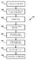
[0077] Each of the aspects and embodiments of the present invention described herein can be used alone or in combination with another. Aspects and embodiments will now be described with reference to the accompanying drawings.
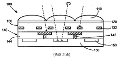
도 1은 종래의 전면측-조명 센서의 단면도를 도시한다.
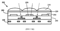
도 2는 종래의 배면측-조명 센서의 단면도를 도시한다.
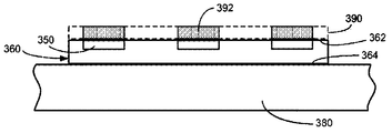
도 3a 내지 도 3c는 다양한 제조 스테이지들에서, 배면측-조명 센서의 실시예의 단면도들이다.
도 4는 본 발명의 예시적인 방법의 흐름도이다.
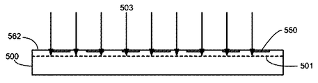
도 5a 내지 도 5c는 다양한 제조 스테이지들에서 배면측-조명 센서의 다른 실시예의 예시적인 단면도들을 도시한다.
도 6은 본 발명의 다른 예시적인 방법의 흐름도이다. Figure 1 shows a cross-sectional view of a conventional front side-illuminated sensor.
2 shows a cross-sectional view of a conventional backside-illuminated sensor.
Figures 3A-3C are cross-sectional views of embodiments of a back side-illumination sensor in various manufacturing stages.
4 is a flow diagram of an exemplary method of the present invention.
Figures 5A-5C illustrate exemplary cross-sectional views of another embodiment of a back side-illumination sensor in various fabrication stages.
6 is a flow chart of another exemplary method of the present invention.
[0014] 배면측-조명 센서는 마무리된 센서 디바이스에 대한 원하는 두께와 실질적으로 등가의 두께를 갖는 박판(lamina)을 이용하여 제조된다. 몇몇 실시예들에서, 박판은 도핑된 영역들이 박판의 전면 표면에 그리고 그 내에 형성되는 프리-스탠딩(free-standing) 박판으로서 제공될 수 있다. 다른 실시예들에서, 도핑된 영역들은 반도체 도너 바디의 제 1 표면에 형성되고, 박판은 도너 바디로부터 클리빙(cleaved)되며, 여기서 도핑된 영역들은 박판의 전면 표면에 그리고 그 내부에 있다. 본 명세서에서 개시되는 방법들은 쓰루풋을 개선하고 제조 비용을 감소시키는 것을 가능케 한다. [0014] The back side-illumination sensor is fabricated using a lamina having a thickness substantially equivalent to the desired thickness for the finished sensor device. In some embodiments, the foil may be provided as a free-standing foil in which doped regions are formed in and on the front surface of the foil. In other embodiments, doped regions are formed on the first surface of the semiconductor donor body, and the thin plate is cleaved from the donor body, wherein the doped regions are on and within the front surface of the foil. The methods disclosed herein enable improved throughput and reduced manufacturing costs.
[0015] 도 1은 렌즈들(110), 컬러 필터(120), 집적 회로(130), 금속 상호연결 층(140), 도핑된 영역(150) 및 반도체 기판(160)을 포함하는 종래의 FSI 센서(100)의 단순화된 도면을 도시한다. 반도체 기판(160)은 제 1 전도성을 가지며 예를 들어, 실리콘일 수 있다. 도핑된 영역들(150)은 반도체 기판(160)과 상이한 전도성으로 도핑된다. 예를 들어, 반도체 기판(160)은 p-타입 전도체일 수 있는 반면에, 도핑된 영역들은 n-타입일 수 있다. 고갈 지역은 p-n 접합에 형성되어 전계를 생성한다. 도핑된 영역들(150) 및 반도체 기판(160) 간의 p-n 접합은 광다이오드를 형성한다. 화살표들(170)에 의해 표시되는 입사 광자들은 전자들이 원자가 대역으로부터 전도 대역이 되게 하여, 자유 전자-홀 쌍들을 생성할 것이다. p-n 접합의 전계 내에서, 전자들은 다이오드의 n 영역 쪽으로 이동하는 경향이 있는 반면에, 홀들은 p 영역 쪽으로 이동하여 결과적으로 광전류라 불리는 전류를 발생시킨다. 통상적으로, 하나의 영역의 도펀트 농도는 다른 영역의 도펀트 농도보다 높을 것이어서, 접합은 n-/p+ 접합 또는 p-/n+ 접합 중 어느 하나가 될 것이다. 1 illustrates a conventional FSI
[0016] 도 1의 FSI 센서(100)에서, 금속 상호연결 층(140)은 배선 또는 상호연결들(142) 및 유전체(144)를 포함할 수 있다. 유사하게, 집적 회로(130)는 또한 배선(132)을 포함한다. 광(170)은 FSI 센서(100)의 "전면측"에 진입하며, 여기서 몇몇 광선들이 배선(132) 및 배선(142)에 의해 차단되거나 반사된다, 도핑된 영역들(150)에 도달하는 광 에너지는 이어서 집적 회로(130)에 의해 프로세싱되는 전기 신호들로 변환된다. [0016] In the
[0017] 도 2는 종래의 BSI 센서(200)의 단순화된 도면이다. BSI 센서는 본질적으로 인버팅된 FSI이어서, 광은 반도체 기판을 통해 배면측에 진입한다. 도 2에서, 화살표(270)에 의해 표시되는 입사광은 렌즈(210)에 진입하고, 커러 필터(220)를 관통하고 이어서 반도체 기판(260)을 통해 다이오드 영역(250)으로 진행하여, 금속 상호연결 층(240) 및 집적 회로(230)의 배선에 의해 방해받지 않는다. 따라서, 광자들을 캡처하는 효율이 FSI 센서들에 비해 BSI 센서들의 경우 크게 증가된다. 그러나 광이 도핑된 영역들(250)에 도달하도록 허용하기에 충분히 얇은 반도체 기판(260)을 제조하는 것은, 기판(260)이 또한 두께 면에서 높은 정밀한 균일도 및 프로세싱 동안 박막 반도체에 대한 손상의 방지를 요구하기 때문에 매우 어렵게 될 수 있다. 그린딩은 통상적으로 실리콘 웨이퍼를 박화(thin)하는데 이용되지만, 웨이퍼 레벨 그린딩은 공통적으로 웨이퍼에 걸친 두께의 변동을 초래한다. 그러므로 부가적인 다이 레벨 폴리싱이 종종 수행된다. 다수의 물질 제거 단계들에 대한 요구는 더 낮은 쓰루풋, 더 높은 비용, 표면 오염의 증가된 위험 및 증가된 핸들링으로 인한 반도체 기판에 대한 손상의 가능성과 같은 다양한 이슈들을 생성한다. [0017] FIG. 2 is a simplified diagram of a
[0018] 도 3a 내지 도 3c는 마무리된 센서 어셈블리에 대해 요구되는 원하는 두께와 실질적으로 등가의 두께를 이미 갖는 박막 반도체 박판을 활용하여 BSI 센서가 제조되는 본 개시의 실시예의 단면도들을 도시한다. 박판은 1 내지 20미크론(㎛) 또는 1 내지 10㎛ 두께와 같이 50㎛ 두께 미만일 수 있다. 제공된 박판의 두께는 예를 들어, BSI 센서의 제조를 위한 프로세싱 단계들 동안 그의 초기 제공된 두께의 적어도 80% 내에서 실질적으로 변경되지 않은 채로 유지된다. [0018] Figures 3A-3C illustrate cross-sectional views of embodiments of the present disclosure in which a BSI sensor is fabricated utilizing a thin film semiconductor laminate already having a thickness that is substantially equivalent to the desired thickness desired for a finished sensor assembly. The thin plate may be less than 50 microns thick, such as 1 to 20 microns (mu m) or 1 to 10 microns thick. The thickness of the provided lamina remains substantially unchanged within at least 80% of its initially provided thickness during processing steps, for example, for the manufacture of a BSI sensor.
[0019] 도 3a에서, 박막 반도체 박판(360)이 제공되며, 여기서 반도체 박판(360)은 전면 표면(362), 배면 표면(364) 및 제 1 전도성을 갖는다. 박판(360)은 전면 표면(362) 및 배면 표면(364) 간에 측정된 두께를 갖는다. 반도체 박판(360)은 박막의 핸들링을 돕기 위해 배면 표면(364)에서 임시 지지부(380)에 의해 접촉될 수 있다. 임시 지지부(380)는 진공, 정전기 또는 화학력과 같이 임의의 타입의 분리 가능한 힘 또는 접착에 의해 박판(360)에 접촉될 수 있다. 몇몇 실시예들에서, 반도체 박판(360)은 도핑된 n-타입 또는 p-타입 단결정질 실리콘일 수 있다. 도핑 농도는 예를 들어, 약 1x10¹⁵ 내지 약 1x10¹⁸ 도펀트 atoms/cm3 또는 예를 들어, 약 1x10¹⁷ 도펀트 atoms/cm3일 수 있다. 하나 이상의 도핑된 영역들(350)이 전면 표면(362)에서 반도체 박판(360) 내에 형성되며, 여기서 도핑된 영역들(350)은 반도체의 전도성과 상이한 전도성을 갖는다. 본 발명의 일 양상은 50㎛ 두께 미만과 같이 임의의 두께의 임의의 박판 상에 형성될 수 있다는 것이다. 본 발명의 다른 양상은 박리 프로세스에 의해 생성될 수 있는 박판의 결함이 도핑된 다이오드 영역들의 제조 이전에 수선(repair)될 수 있다는 것이다. [0019] In FIG. 3A, a thin film semiconductor
[0020] 도 3a의 도핑된 영역들(350)은 확산 도핑을 포함해서 당 분야에 알려진 방법들에 의해 형성될 수 있다. 예를 들어, 도 3a에서 도시된 바와 같이, 도핑된 유리층(390)이 대기압 PCVD(atmospheric pressure chemical vapor deposition)와 같은 임의의 방법에 의해 전면 표면(362) 상에 형성될 수 있다. p-타입 도펀트에 대해, 도핑된 유리층(390)은 예를 들어, 붕소로 도핑된 BSC(horosilicaie glass)일 수 있다. 소스 가스는 붕소 예를 들어, BBr3, B2H6, 또는 BCl3를 제공할 임의의 적합한 가스일 수 있다. n-타입 도펀트에 대해, POCl3와 같은 적절한 가스가 전면 표면(362) 상에 약 30분 동안 약 880℃에서 유동되어, PSG(phosphosiiicate glass)를 형성할 수 있다. 다른 실시예들에서, 도펀트-제공 물질은 전면 표면(362) 상에서 회전(spun)되고 베이크(bake)될 수 있다. 또 다른 실시예들에서, 도핑된 유리는 BN과 같은 고체 소스 상에 O2를 유동시킴으로써 열적으로 성장될 수 있다. 도핑된 유리층(390)은 예를 들어, 약 500 내지 약 1500 옹스트롬, 예를 들어, 약 1000 옹스트롬의 두께를 가질 수 있다. 다음으로, 도핑된 유리(390)는 예를 들어, 스크린 프린팅 에천트 페이스트(screen printing etchant paste)에 의해 선택된 영역들에서 제거되어, 도핑된 영역들(350)이 형성되는 유리 영역들(392)(음영진 영역들로 도시됨)을 남긴다. 대안적으로, 도핑된 영역들(350)은 n-타입 도펀트를 포함하는 비정질 실리콘의 증착에 의해 전면 표면(362) 상에 형성될 수 있다. 몇몇 실시예들에서, 비정질 실리콘의 고유(도핑되지 않은)층은 도핑된 비정질 실리콘층과 전면 표면(362) 간에 개재될 수 있다. [0020] The doped
[0021] 도핑된 영역(350)을 형성하기 위한 대안적인 프로세스에서, Si3N4(도시되지 않음)가 전면 표면(362) 상에 증착될 수 있다. 스크린 프린트 에천트 페이스트는 도핑된 영역들(350)이 형성되지 않는 전면 표면(362) 상의 임의의 위치들을 마스킹하도록 Si3N4를 에칭하기 위해 적용된다. 대안적으로, 종래의 포토리소그라피 기법들이 이들 마스킹된 영역들을 정의하는데 이용될 수 있다. 인(예를 들어, POCl3)의 소스를 이용하는 확산 도핑이 n-타입 도핑된 영역들을 형성하도록 수행되어, 붕소-함유 대기(예를 들어, BBr3)가 노출된 영역들에서 p-타입 영역들을 형성하도록 이용된다. 임의의 잔여 Si3N4는 HF(hydrofluoric acid)와 같이 알려진 방법들을 이용하여 그 시간에 에칭될 수 있다. 얇은 산화물 층이 웨이퍼 상에서 성장될 수 있다. [0021] In an alternative process for forming the doped
[0022] 예를 들어, 약 850 내지 약 1000℃의 어닐링이 약 30분 내지 약 90분 동안 노(furnace)에서 수행되고, 전면 표면(362)에서 유리 영역(392)으로부터 반도체 박판(360)으로 도펀트들을 확산한다. 확산은 도핑된 P-타입(예를 들어, BSG로부터) 또는 n-타입(예를 들어, PSG로부터) 영역들(350) 중 어느 하나를 형성한다. 다음으로, 종래의 습식 에칭, 예를 들어, HF 딥(dip)은 전면 표면(362)에서 노출된 도핑된 영역들(350)을 남기도록 BSG 또는 PSG를 제거한다. 붕소 및 인은 각각 가장 흔히 이용되는 p-타입 및 n-타입 도펀트들이지만, 다른 도펀트들이 이용될 수 있다. For example, an anneal at about 850 to about 1000 ° C is performed in a furnace for about 30 minutes to about 90 minutes, and from the
[0023] 도핑된 영역들(350)이 박막 반도체 박판(360)에 형성된 이후, 전기 연결들이 도 3b에서 도시된 바와 같이 형성될 수 있다. 몇몇 실시예들에서, 전기 연결은 금속화층(340)에서 하나 이상의 서브-층들을 포함할 수 있다. 금속화층(340)은 예를 들어, 물리적 기상 증착을 이용한 스퍼터 증착에 의해 형성될 수 있다. 금속화층들(340)은 예를 들어, 티타늄, 티타늄-텅스텐, 또는 구리를 포함할 수 있다. 당 분야에 알려진 포토리소그라피 방법들이 도 3c에서 도시된 바와 같이 도핑된 영역들(350)로의 전기 연결들(342)을 형성하기 위해 금속화층들(340)에서 원하는 배선 패턴들을 마스킹 및 에칭하는데 이용될 수 있다. 후속 제조 단계들은 이어서 박막 반도체 박판(360)으로부터 배면측-조명 센서를 제조하기 위해 실행될 수 있다. 예를 들어, 구리-주석, 구리-인듐 또는 인듐-주석 범프들(344)은 집적 회로(330)의 본딩을 용이하게 하기 위해 금속화층들(340) 상에 전기도금될 수 있다. 이 본딩은 구리 및 주석 또는 인듐 및 인듐 또는 인듐 및 주석을 이용하여, 집적 회로와 박판 간의 전기 연결들을 발생시킬 수 있는 임의의 알려진 방법, 예를 들어, 구리-구리 열-압축 본딩, 또는 고체-액체 인터-확산 본딩을 이용하여 달성될 수 있다. 몇몇 실시예들에서, 집적 회로(330)는 CMOS(complementary metal-oxide semiconductor)일 수 있다. After the doped
[0024] 원하는 컴포넌트들이 박막 반도체(360)의 전면 표면(362) 상에 구성된 이후, 임시 지지부(380)가 박판(360)의 배면 표면(364)으로부터 제거된다. 완성된 BSI 센서는 예를 들어, 코팅들, 컬러 필터들 및 마이크로-렌즈들을 배면 표면(364)에 부가함으로써 제조될 수 있다(예를 들어, 도 2). 도 3a 내지 도 3c의 실시예들에서 알 수 있는 바와 같이, 초기 제공된 박막 반도체 박판(360)의 두께는 배면측 조명 센서의 제조 동안 실질적으로 변경되지 않은 채로 유지되며, 이에 따라 그린딩에 의해 생성되는 이슈를 감소시킨다. [0024] After the desired components are configured on the
[0025] 도 4의 흐름도(400)는 도 3a 내지 도 3c의 실시예들을 예시한다. 흐름도(400)의 예시적인 방법은 단계(410)에서 박막 반도체 박판을 제공하는 것으로 시작한다. 단계(420)에서, 임시 캐리어 또는 지지부가 프로세싱 동안 취약한 박판의 핸들링을 지원하기 위해 박판의 배면 표면에 대해 접촉될 수 있다. 하나 이상의 도핑된 영역들은 단계(430)에서 박판의 전면 표면에 형성되며, 여기서 도핑된 영역들이 박막 반도체의 전도성과 반대의 전도성을 갖는다. 단계(440)에서, 하나 이상의 전기 연결들이 도핑된 영역에 대해 형성된다. 전기 연결들은 예를 들어, 금속화층들, 솔더 범프들 및 열-압축 인터페이스들을 포함할 수 있다. 임시 캐리어가 단계(450)에서 제거되며, 그 이후 마무리된 배면측-조명 센서는 원할 때 박판의 배면 표면 상에서 임의의 부가적인 제조 단계들을 수행함으로써 단계(460)에서 제조될 수 있다. 이들 마무리하는 단계들은 예를 들어, 코팅들, 컬러 필터들 및 마이크로-렌즈들을 부가하는 것을 포함할 수 있다. 코팅들은 박판의 배면 표면을 패시배이팅(passivate)하는 층들을 포함할 수 있다. 이들 패시배이션 층들은 450℃ 미만의 온도에서 플라즈마-강화된 화학 기상 증착에 의해 증착되는 수소화된 비정질 실리콘의 10Å 내지 300Å 층을 포함할 수 있다. 마무리하는 단계들은 클리빙 주입 프로세스(cleaving implant process) 동안 초래되는 손상을 제거하기 위해 박판의 배면 표면으로부터 일부 물질을 에칭하는 것을 또한 포함할 수 있다. [0025] The
[0026] 본 개시의 다른 실시예는 도 5a 내지 도 5c에서 도시된다. 이 실시예에서, 도 5a의 도핑된 영역들(550)은 반도체 도너 바디(500)에 형성되고, 이어서 박판이 반도체 도너 바디(500)로부터 클리빙되며, 여기서 박판은 도핑된 영역들(550)을 포함한다. 도너 바디(500)는 임의의 실제 두께 예를 들어, 약 200 내지 약 1000 미크론 두께의 단결정질 실리콘 웨이퍼와 같은 적절한 반도체 물질이다. 대안적인 실시예들에서, 도너 웨이퍼는 더 두꺼울 수 있고; 최대 두께는 웨이퍼 핸들링의 실용성들(practicalities)에 의해서만 제한된다. 대안적으로, GaAs, InP 등과 같이 게르마늄, 실리콘 게르마늄, 또는 III-V 또는 II-VI 반도체 화합물들을 포함하는 다른 반도체 물질의 웨이퍼들 또는 잉곳(ingot)들이 이용될 수 있다. [0026] Another embodiment of the present disclosure is illustrated in Figures 5A-5C. In this embodiment, the doped
[0027] 단결정질 실리콘을 형성하는 프로세스는 일반적으로 원형 웨이퍼를 발생시키지만, 도너 바디는 다른 형상들을 또한 가질 수 있다. 실린더형 단결정질 잉곳들은 종종 웨이퍼들을 절단하기 이전에 8각 단면으로 머시닝된다. 다결정질 웨이퍼들은 종종 직사각형이다. 직사각형 웨이퍼들은 원형 또는 6각형 웨이퍼들과 달리, 이들이 그들 간에 최소의 미사용 갭들을 갖도록 에지-대-에지로 정렬될 수 있다는 이점을 갖는다. 웨이퍼의 직경 또는 폭은 임의의 표준 또는 관습적인 크기일 수 있다. 단순함을 위해, 본 개시는 반도체 도너 바디로서 단결정질 실리콘 웨이퍼의 이용을 설명하지만, 다른 타입들 및 물질들의 도너 바디들이 이용될 수 있다는 것이 이해될 것이다. [0027] The process of forming monocrystalline silicon generally produces a circular wafer, but the donor body may also have other shapes. Cylindrical single crystal ingots are often machined to octagonal cross-sections prior to cutting the wafers. Polycrystalline wafers are often rectangular. Rectangular wafers, unlike circular or hexagonal wafers, have the advantage that they can be aligned edge-to-edge with minimal unused gaps between them. The diameter or width of the wafer may be any standard or customary size. For simplicity, the present disclosure describes the use of monocrystalline silicon wafers as semiconductor donor bodies, but it will be understood that donor bodies of other types and materials may be used.
[0028] 도핑된 영역들(550)을 포함하는 박판의 박리는 이온 유도 클리비지 반응(ion induced cleavage reaction)을 포함하는 임의의 조치에 의해 발생할 수 있다. Sivaram 등에 의해 2008년 2월 5일 출원되고, 본 발명의 양수인에 의해 소유되며, 그에 의해 인용에 의해 포함되는, 발명의 명칭이 "Method to Form a Photovoltaic Cell Comprising a Thin Lamina"인 미국 특허 출원 번호 제12/026530호는 가스 이온들 예를 들어, 수소 및/또는 헬륨 이온들의 하나 이상의 종들로 주입되는 (도핑 영역들(550) 없는) 반도체 도너 웨이퍼를 설명한다. 주입된 이온들은 반도체 도너 웨이퍼(500) 내에서 도 5a의 클리브 플래인(501)과 같은 클리브 플래인을 정의한다. 본 개시에서 도너 바디로서 또한 지칭되는 반도체 도너 웨이퍼(500)는 추후에-박리되는 박판의 전면 표면(562)이 되는 제 1 표면(562)을 갖는다. 가스 이온들은 클리브 플래인(501)을 생성하도록 제 1 표면(562)을 통해 (화살표(503)에 의해 표시된 바와 같이) 주입된다. 이 수소 또는 헬륨 주입의 비용은 Parrill 등에 의해 2008년 5월 16일 출원되고, 발명의 명칭이 "Ion Implanter for Photovoltaic Cell Fabrication"이며, 본 발명의 양수인에 의해 소유되고 그에 의해 인용에 의해 포함되는, 미국 특허 출원 번호 제12/122108호에서 설명된 방법들에 의해 감소될 수 있다. 제 1 표면(562)으로부터 측정된 바와 같은 클리브 플래인(501)의 전체 깊이는 주입 에너지를 포함하는 몇 개의 팩터들에 의해 결정된다. 클리브 플래인(501)의 깊이는 제 1 표면(562)으로부터 약 0.2 내지 약 100㎛, 예를 들어, 약 0.5 내지 약 20㎛; 또는 약 0.5 내지 약 50㎛, 예를 들어, 약 1 내지 약 25㎛, 또는 약 8 미크론 내지 약 20㎛일 수 있다. 클리브 플레인(501)의 깊이는 클리빙된 박판의 두께를 결정할 것이다. 바람직하게는, 클리빙된 박판의 두께는 완성된 BSI 센서에서 반도체 기판의 원하는 두께와 실질적으로 등가가 되도록 선택된다. 따라서 본 발명의 실시예들에 따라 BSI에 대한 반도체 기판은 유리하게는 두께면에서 매우 정밀한 균일도를 갖고 특히 원하는 두께를 갖도록 생성될 수 있다.[0028] The delamination of the thin plate including the doped
[0029] 도 5b에서 도시된 바와 같이, 어닐링 반응은 박판(560)이 클리브 플레인(501)에서 도너 웨이퍼(500)로부터 클리빙하게 하며, 여기서 클리브 플래인(501)은 박판(560)의 배면 표면(564)을 생성한다. 반도체 도너 바디(500)의 제 1 표면(562)은 박판(560)의 전면 표면(562)이 된다. 도너 웨이퍼(500)는 제 1 표면(562)에서 반도체 도너 바디(500)로부터 박판(560)을 리프트하는데 이용될 수 있는 임시 지지부 엘리먼트(585)에 부착된다. 5B, the annealing reaction causes the
[0030] Sivaram 등의 실시예들에 따라, 반도체 박판(560)은 약 0.2 내지 약 100㎛ 두께, 예를 들어, 약 0.2 내지 약 50㎛, 예를 들어, 약 1 내지 약 25㎛ 두께, 몇몇 실시예들에서, 약 5 내지 약 20㎛ 두께일 수 있지만, 지명된 범위 내의 임의의 두께도 가능하다. Sivaram 등의 방법들을 이용하면, 광전지 셀들은 불필요하게 두꺼운 셀의 제조에 의해 또는 과도한 커프 손실(excessive kerf loss)을 통해 실리콘을 낭비함 없이, 슬라이싱된 웨이퍼로부터 형성되는 것보단 오히려 얇은 반도체 박판으로 형성되고, 이에 따라 비용을 감소시킨다. 동일한 도너 웨이퍼는 비용을 추가로 감소시키도록 다수의 박판을 형성하기 위해 재사용될 수 있고, 몇몇 다른 이용을 위해 다수의 박판의 박리 이후에 재판매될 수 있다. According to embodiments such as Sivaram, the semiconductor
[0031] 그렇지만, Sivaram 등의 방법들에서, 웨이퍼는 얇은 박판에 대한 기계적 지지부를 제공하기 위해 프로세스에서 앞서 임시 또는 영구 지지부 엘리먼트에 접촉되어야 한다. 통상적으로, 이러한 방식으로 형성된 박판은 지지부 엘리먼트를 제거하기 위해 분리 단계에 참여하거나 임의의 결과적인 디바이스에 지지부 엘리먼트를 통합해야 한다. 본 개시의 몇몇 실시예들에서, 얇은 프리-스탠딩 박판이 형성되고 지지부 엘리먼트에 대한 영구적 본딩 또는 접착 없이 그리고 박판으로부터 디바이스를 제조하기 이전의 분리 또는 세척 단계들을 요구함 없이 도너 바디로부터 분리될 수 있어서, 박판의 전면 또는 배면 표면에 대한 임의의 수의 프로세싱 단계들을 유익하게 제공한다. 도너 바디(500)의 제 1 표면(박리된 박판의 전면 표면일 것임)은 지지부 엘리먼트(585)에 인접하게 배치되고, 표면이 프로세싱 단계들로 처리되기 이전에 또는 이후에 도너 바디의 제 1 표면으로부터 박판을 박리하는 어닐링 단계가 수행될 수 있다. 클리빙된 플래인은 박판의 배면 표면을 생성하고, 재차 다시 한번, 임의의 수의 프로세싱 단계들이 이어서 박리된 박판의 어느 한 측 상에서 발생할 수 있다. 이들 프로세스들은 Kell 등에 의해, 2011년 12월 20일 출원되고, 그에 의해 인용에 의해 포함되는, 발명의 명칭이 "A Method and Apparatus for Forming a Thin Lamina"인 미국 특허 출원 번호 제13/331,909호에서 설명된 바와 같이 박판 상에 본딩된 지지부 엘리먼트 없이 발생할 수 있다. [0031] However, in the methods of Sivaram et al., The wafer must contact the temporary or permanent support element in advance in the process to provide a mechanical support for the thin lamina. Typically, the sheet formed in this manner must either participate in the separation step or incorporate the support element into any resulting device to remove the support element. In some embodiments of the present disclosure, a thin pre-standing thin sheet can be formed and detached from the donor body without requiring permanent bonding or adhesion to the support element and requiring separation or cleaning steps prior to manufacturing the device from the sheet, Advantageously provides any number of processing steps for the front or back surface of the foil. The first surface of the donor body 500 (which will be the front surface of the stripped lamina) is disposed adjacent to the
[0032] 도 5c로 넘어가서, 박리 이전에, 본 발명의 반도체 도너 바디(500)의 제 2 표면(502)은 서셉터 어셈블리와 같은 임시 지지부 엘리먼트(586)에 분리 가능하게 접촉될 수 있다. 도너 바디(500)와 지지부 엘리먼트(586) 간의 접촉은 진공, 정전기 또는 화학력과 같이 임의의 타입의 분리 가능한 힘 또는 접착을 포함할 수 있다. 몇몇 실시예들에서, 박판의 박리 동안 도너 바디(500)와 서셉터(586) 간의 상호작용 힘은 단지 서셉터(586) 상의 도너 바디(500)의 무게이다. 박리 장비가 도 5b에서 도시된 것으로부터 수직으로 인버팅되는 구성을 갖는 다른 실시예들에서, 상호작용 힘은 단지 도너 바디 상의 서셉터 어셈블리(586)의 무게이다. 도너 바디(500)와 서셉터 어셈블리(586)의 접촉에 이어, 열 또는 다른 힘이 클리브 플래인(501)에서 도너 바디(500)로부터 박판(560)을 클리빙하도록 도너 바디(500)에 인가될 수 있다. 박리 조건들은 영구적으로 부착되는 지지부 엘리먼트 없이, 박리되는 박판에서 물리적 결함들을 최소화하기 위해 도너 바디로부터 박판을 클리빙하도록 최적화될 수 있다. 박리는 예를 들어, 약 350 내지 약 650℃의 온도들에서 수행될 수 있다. 일반적으로 박리는 더 높은 온도에서 더 빨리 진행된다. [0032] Turning to FIG. 5C, prior to stripping, the
[0033] 클리브 플래인(501)에서 도너 웨이퍼(500)로부터 박판(560)을 클리빙하는데 있어서, 박판(560)의 전면 표면(562)에 대향하는 배면 표면(564)은 도 5c에서 도시된 바와 같이 생성된다. 도핑된 영역들(550)은 박판(560) 내에 그리고 전면 표면(562)에 위치된다. 박판(560)은 이온 주입에 의해 야기되는 임의의 손상을 제거하기 위해 어닐링될 수 있다. 프리-스탠딩 박판(560)은 임시 지지부 엘리먼트에 전면 표면(562) 또는 배면 표면(564) 중 어느 하나에서 임시로 접촉될 수 있다. 예를 들어, 도 5c의 지지부 엘리먼트(580)는 추가의 제조 단계들 동안 배면 표면(564)에 다시 접촉하고, 위의 도 3b 내지 도 3c에 관해 설명된 바와 같이 박판(560)을 배면측-조명 센서로 제조하기 위해 추후에 제거된다. In cleaving the
[0034] 이온들을 주입하고, 반도체 도너 바디를 클리빙하고 도핑된 영역들을 형성하는 단계들은 450℃ 초과와 같은 높은 온도들에서 발생한다는 것에 주의한다. BSI 센서를 제조하는 앞선 스테이지들에서 이런 높은 온도 단계들을 수행하는 것은 유리하게는 보다 열적으로 약한 물질들이 배면측-조명 센서를 제조하는 추후의 단계들에서 이용되도록 허용한다. 본 발명의 몇몇 실시예들에서, 완성된 BSI 센서의 제조 동안, 이온들을 주입하고, 반도체 도너 바디를 클리빙하고 도핑된 영역을 형성하는 단계들만이 약 450℃ 초과의 프로세싱 온도들을 갖는다. 다른 실시예들에서, 도핑 영역을 형성하는 것은 이온들을 주입하는 단계 이전에 발생한다. It should be noted that steps of implanting ions, cleaving the semiconductor donor body and forming doped regions occur at high temperatures, such as above 450 ° C. Performing these high temperature steps in the previous stages of manufacturing the BSI sensor advantageously allows the more thermally weak materials to be used in later steps to fabricate the back side-illumination sensor. In some embodiments of the invention, during fabrication of the completed BSI sensor, only the steps of implanting ions, cleaving the semiconductor donor body and forming the doped region have processing temperatures above about 450 [deg.] C. In other embodiments, forming the doped region occurs prior to implanting the ions.
[0035] 도 6의 흐름도(600)는 도 5a 내지 도 5c의 방법들의 예시적인 실시예를 예시한다. 단계(610)에서, 반도체 도너 바디가 제공된다. 마무리된 BSI 센서 어셈블리의 광다이오드로서 역할하게 되는 하나 이상의 도핑된 영역들이 단계(620)에서 도너 바디에 형성된다. 도핑된 영역들은 도너 바디의 제 1 표면에 형성되고 도너 바디의 전도성과 상이한 전도성을 가진다. 이온들이 단계(630)에서 클리브 플래인을 형성하도록 반도체 도너 바디 내로 주입되고 이어서 반도체 박판이 단계(640)에서 도너 바디로부터 클리빙된다. 반도체 바디의 제 1 표면은 박판의 제 1 표면으로서 역할하고, 클리브 플래인은 박판의 배면 표면을 생성한다. 또한, 도핑된 영역들은 박리된 박판의 전면 표면에 포함된다. 단계(650)에서, 임시 캐리어 또는 지지부는 반도체 박판의 배면 표면에 접촉된다. 위에서 설명된 금속화층들과 같은 전기 연결들이 단계(660)에서 박판의 전면측 상의 도핑된 영역들에 커플링된다. 임시 캐리어가 단계(670)에서 제거된다. 마무리된 배면측-조명 센서는 도 4의 단계(460)에 관해 설명된 것들과 같이 박판의 배면 표면 상에 요구되는 임의의 부가적인 제조 단계들을 수행함으로써 단계(680)에서 제조될 수 있다. [0035] The
[0036] 위에서 논의된 바와 같이, 본 발명의 실시예들은 BSI 센서에 대한 원하는 두께를 달성하기 위해 추가의 박화를 요구하지 않는 박판을 제공하고, 이에 따라 비용을 감소시키고 제조성을 개선하는 방법을 제공한다. 제공된 박판의 두게는 실질적으로 변경되지 않은 채로 유지되는데, 이를 테면, 예를 들어, 에칭 - 박판의 프로세싱 및 배면측-조명 센서의 제조 동안 - 의 결과로서 기껏해야 그의 초기 두께의 20까지 변형된다. 방법들의 실시예들은 또한 제조 프로세스에서 앞서 다이오드 영역들을 도핑- 통상적으로 높은 온도를 요구하는 프로세스들 -하는 것을 포함하며, 결과적으로 후속 제조 단계들에서 더 낮은 온도 물질들 및 프로세스들의 이용을 허용한다. [0036] As discussed above, embodiments of the present invention provide a thin sheet that does not require additional thinning to achieve the desired thickness for the BSI sensor, thereby providing a method of reducing cost and improving fabrication do. The thickness of the provided sheet remains substantially unchanged, for example, up to 20 of its initial thickness at most as a result of, for example, the processing of the etch-sheet and the fabrication of the backside-light sensor. Embodiments of the methods also include doping the diode regions in advance in the fabrication process-typically processes that require high temperatures, resulting in the use of lower temperature materials and processes in subsequent fabrication steps.
[0037] 부가적인 단계들이 본 발명의 범위로부터 벗어남 없이 본 개시에서 설명되는 흐름도에 포함될 수 있다는 것이 주의된다. 예를 들어, 몇몇 실시예들에서, 임시 지지부는 전면 표면에 또한 접촉될 수 있다. 유사하게, 전면 및 배면 표면들 중 어느 하나 또는 둘 다에 접촉하는 임시 지지부들은 마무리된 BSI 센서 어셈블리의 제조에 수반되는 다양한 단계들을 통해 박판을 전달하는데 이용될 수 있다. 다른 실시예들에서, 에칭 또는 다른 표면 준비 프로세스들이 수행될 수 있다. 에칭 단계는 박판의 배면 표면에서 손상을 제거하도록 역할할 수 있다. 이 에칭 단계는 예를 들어, 습식 또는 플라즈마 처리에 의해 수행될 수 있다. 플라즈마 처리는 예를 들어, SF6 대기에서 발생할 수 있다. 에칭된 양은 총 박판 두께의 20% 미만일 수 있다. [0037] It is noted that additional steps may be included in the flowcharts described in this disclosure without departing from the scope of the present invention. For example, in some embodiments, the temporary support may also contact the front surface. Similarly, temporary supports that contact either or both of the front and back surfaces can be used to deliver the sheet through various steps involved in the fabrication of the finished BSI sensor assembly. In other embodiments, etching or other surface preparation processes may be performed. The etching step may serve to remove damage from the back surface of the foil. This etching step can be performed, for example, by wet or plasma treatment. Plasma processing can occur, for example, in an SF 6 atmosphere. The etched amount may be less than 20% of the total sheet thickness.
[0038] 본 명세서가 본 발명의 특정한 실시예들에 관해 상세히 설명하였지만, 당업자들은, 위의 내용을 이해하면, 이들 실시예들에 대한 변경들, 그의 변동물들, 및 그의 등가물들을 쉽게 생각해낼 수 있다는 것이 인지될 것이다. 본 발명에 대한 이들 및 다른 변형들 및 변동물들은, 특히 첨부된 청구항들에서 제시되는 본 발명의 사상 및 범위로부터 벗어남 없이 당업자들에 의해 실시될 수 있다. 또한, 당업자들은 위의 설명은 단지 예이며 본 발명을 제한하는 것으로 의도되지 않는다는 것을 인지할 것이다.
[0038] While the specification has been described in some detail with reference to specific embodiments thereof, those skilled in the art will readily appreciate that many modifications may be made to adapt a particular embodiment without departing from the spirit and scope of the invention. ≪ / RTI > These and other modifications and variations of the present invention may be practiced by those skilled in the art without departing from the spirit and scope of the invention, which is set forth with particularity in the appended claims. In addition, those skilled in the art will recognize that the above description is merely an example and is not intended to limit the invention.
Claims (22)
전면 표면, 배면 표면 및 상기 전면 표면과 상기 배면 표면 간의 두께를 갖는 박막 반도체 박판(thin film semiconductor lamina)을 제공하는 단계 - 상기 반도체 박판은 제 1 전도성을 가짐 - ;
상기 박판의 전면 표면에서 상기 반도체 박판 내에 도핑된 영역을 형성하는 단계 - 상기 도핑된 영역은 제 2 전도성을 가짐 -;
상기 반도체 박판의 배면 표면에 임시 캐리어를 접촉시키는 단계;
상기 반도체 박판의 전면측에 상기 도핑된 영역에 대한 전기적 연결을 형성하는 단계;
상기 배면 표면으로부터 상기 임시 캐리어를 제거하는 단계; 및
상기 반도체 박판으로부터 배면측-조명 센서를 제조하는 단계
를 포함하고,
상기 반도체 박판의 두께는 상기 배면측 조명 센서의 제조 동안 실질적으로 변경되지 않은 채로 유지되는,
배면측-조명 센서를 제조하는 방법.A method of manufacturing a backside-illuminated sensor,
Providing a thin film semiconductor lamina having a front surface, a back surface, and a thickness between the front surface and the back surface, the thin semiconductor lamina having a first conductivity;
Forming a doped region in the semiconductor thin plate at a front surface of the thin plate, the doped region having a second conductivity;
Contacting a temporary carrier to the back surface of the semiconductor thin plate;
Forming an electrical connection to the doped region on the front side of the semiconductor thin plate;
Removing the temporary carrier from the backside surface; And
A step of manufacturing a back side-illumination sensor from the semiconductor thin plate
Lt; / RTI >
Wherein the thickness of the semiconductor thin plate remains substantially unchanged during manufacture of the back side illumination sensor,
Backside-light sensor.
제 1 표면을 갖는 반도체 도너 바디(semiconductor donor body)를 제공하는 단계 - 상기 반도체 도너 바디는 제 1 전도성을 가짐 - ;
클리브 플래인(cleave plane)을 정의하도록 상기 반도체 도너 바디의 제 1 표면에 이온들을 주입하는 단계;
상기 클리브 플래인에서 상기 반도체 도너 바디를 클리빙(cleaving)하는 단계
를 더 포함하고,
상기 클리브 플래인은 상기 반도체 박판의 배면 표면을 형성하고,
상기 반도체 도너 바디의 제 1 표면은 상기 반도체 박판의 전면 표면을 형성하는,
배면측-조명 센서를 제조하는 방법.The method according to claim 1,
Providing a semiconductor donor body having a first surface, the semiconductor donor body having a first conductivity;
Implanting ions into a first surface of the semiconductor donor body to define a cleave plane;
And clearing the semiconductor donor body at the clean plane
Further comprising:
Wherein the clearance plane forms the back surface of the semiconductor thin plate,
Wherein a first surface of the semiconductor donor body forms a front surface of the semiconductor thin plate,
Backside-light sensor.
상기 이온들을 주입하는 단계, 상기 반도체 도너 바디를 클리빙하는 단계, 및 상기 도핑 영역을 형성하는 단계들만이 약 450℃ 초과의 프로세싱 온도들을 갖는,
배면측-조명 센서를 제조하는 방법.3. The method of claim 2,
Implanting the ions, clearing the semiconductor donor body, and forming only the doped region having processing temperatures greater than about < RTI ID = 0.0 > 450 C, < / RTI &
Backside-light sensor.
상기 도핑된 영역을 형성하는 단계는,
상기 이온들을 주입하는 단계 이전에 발생하는,
배면측-조명 센서를 제조하는 방법.3. The method of claim 2,
Wherein forming the doped region comprises:
Which occurs prior to implanting the ions,
Backside-light sensor.
상기 이온들을 주입하는 단계는,
주입 에너지를 포함하고,
상기 주입 에너지는 상기 클리브 플래인의 깊이를 결정하며, 상기 깊이는 상기 반도체 도너 바디의 제 1 표면으로부터 측정되고,
상기 깊이는 상기 반도체 박판의 두께와 실질적으로 등가가 되도록 선택되는,
배면측-조명 센서를 제조하는 방법.3. The method of claim 2,
The step of implanting ions comprises:
Including injection energy,
Wherein the implant energy determines the depth of the cleave plane, the depth being measured from a first surface of the semiconductor donor body,
The depth being selected to be substantially equal to the thickness of the semiconductor thin plate,
Backside-light sensor.
상기 전기적 연결을 형성하는 단계는,
상기 반도체 박판의 전면측에 금속화층을 도포(apply)하는 단계; 및
집적 회로를 상기 금속화층에 커플링하는 단계를 포함하는,
배면측-조명 센서를 제조하는 방법.The method according to claim 1,
Wherein forming the electrical connection comprises:
Applying a metalization layer on the front side of the semiconductor thin plate; And
And coupling the integrated circuit to the metallization layer.
Backside-light sensor.
상기 집적 회로는,
CMOS(complementary metal-oxide semiconductor)인,
배면측-조명 센서를 제조하는 방법.The method according to claim 6,
The integrated circuit comprising:
A complementary metal-oxide semiconductor (CMOS)
Backside-light sensor.
상기 반도체 박판의 배면 표면에 컬러 필터를 커플링하는 단계
를 더 포함하는,
배면측-조명 센서를 제조하는 방법.The method according to claim 1,
Coupling the color filter to the back surface of the semiconductor thin plate;
≪ / RTI >
Backside-light sensor.
상기 박막 반도체 박판의 두께는 약 25 미크론 미만인,
배면측-조명 센서를 제조하는 방법.The method according to claim 1,
Wherein the thin film semiconductor thin plate has a thickness of less than about 25 microns,
Backside-light sensor.
상기 박막 반도체 박판의 두께는 약 1 내지 약 50 미크론인,
배면측-조명 센서를 제조하는 방법.The method according to claim 1,
Wherein the thin film semiconductor thin plate has a thickness of about 1 to about 50 microns,
Backside-light sensor.
상기 반도체 박판의 두께는,
상기 배면측-조명 센서의 제조 동안 그의 초기에 제공된 두께의 20% 편차 내에서 유지되는,
배면측-조명 센서를 제조하는 방법.The method according to claim 1,
The thickness of the semiconductor thin plate is,
Is maintained within a 20% deviation of the thickness initially provided during the manufacture of the backside-illuminated sensor,
Backside-light sensor.
제 1 표면 및 제 1 전도성을 갖는 반도체 도너 바디를 제공하는 단계;
상기 제 1 표면에서 상기 반도체 도너 바디 내에 도핑된 영역을 형성하는 단계 - 상기 도핑된 영역은 제 2 전도성을 가짐 - ;
클리브 플래인(cleave plane)을 정의하도록 상기 반도체 도너 바디의 제 1 표면으로 이온들을 주입하는 단계;
상기 클리브 플래인에서 상기 반도체 도너 바디로부터 반도체 박판을 클리빙하는 단계 - 상기 클리브 플래인은 상기 반도체 박판의 배면 표면을 형성하고, 상기 반도체 도너 바디의 제 1 표면은 상기 반도체 박판의 전면 표면이고, 상기 전면 표면은 상기 도핑된 영역을 포함함 -;
상기 반도체 박판의 배면 표면에 임시 캐리어를 접촉시키는 단계;
상기 반도체 박판의 전면측 상의 상기 도핑된 영역에 대한 전기적 연결을 형성하는 단계;
상기 배면 표면으로부터 상기 임시 캐리어를 제거하는 단계; 및
상기 반도체 박판으로부터 배면측-조명 센서를 제조하는 단계
를 포함하고,
상기 반도체 박판의 전면측과 배면 표면 간의 두께는 상기 배면측-조명 센서의 제조 동안 실질적으로 변경되지 않은 채로 유지되는,
배면측-조명 센서를 제조하는 방법.A method of manufacturing a backside-illuminated sensor,
Providing a semiconductor donor body having a first surface and a first conductivity;
Forming a doped region within the semiconductor donor body at the first surface, the doped region having a second conductivity;
Implanting ions into a first surface of the semiconductor donor body to define a cleave plane;
Wherein the clean surface forms the back surface of the semiconductor thin plate, the first surface of the semiconductor donor body is the front surface of the semiconductor thin plate, The front surface including the doped region;
Contacting a temporary carrier to the back surface of the semiconductor thin plate;
Forming an electrical connection to the doped region on the front side of the semiconductor thin plate;
Removing the temporary carrier from the backside surface; And
A step of manufacturing a back side-illumination sensor from the semiconductor thin plate
Lt; / RTI >
Wherein the thickness between the front side and the backside surface of the semiconductor thin plate remains substantially unchanged during manufacture of the backside-
Backside-light sensor.
상기 전기적 연결을 형성하는 단계는,
상기 반도체 박판의 전면측에 금속화층을 도포하는 단계; 및
상기 금속화층에 집적 회로를 커플링하는 단계를 포함하는,
배면측-조명 센서를 제조하는 방법.13. The method of claim 12,
Wherein forming the electrical connection comprises:
Applying a metallization layer to a front side of the thin semiconductor plate; And
And coupling the integrated circuit to the metallization layer.
Backside-light sensor.
상기 반도체 박판의 배면 표면에 컬러 필터를 커플링하는 단계
를 더 포함하는,
배면측-조명 센서를 제조하는 방법.13. The method of claim 12,
Coupling the color filter to the back surface of the semiconductor thin plate;
≪ / RTI >
Backside-light sensor.
상기 도핑된 영역들을 형성하는 단계는,
이온들을 주입하는 단계 이전에 발생하는,
배면측-조명 센서를 제조하는 방법.13. The method of claim 12,
Wherein forming the doped regions comprises:
Lt; RTI ID = 0.0 > ions, < / RTI >
Backside-light sensor.
상기 박막 반도체 박판의 두께는 약 1 미크론 내지 약 50 미크론인,
배면측-조명 센서를 제조하는 방법.13. The method of claim 12,
Wherein the thickness of the thin film semiconductor thin plate is from about 1 micron to about 50 microns,
Backside-light sensor.
상기 반도체 박판의 두께는 상기 배면측-조명 센서의 제조 동안 그의 초기에 제공되는 두께의 20% 편차 이내에서 유지되는,
배면측-조명 센서를 제조하는 방법.13. The method of claim 12,
Wherein the thickness of the semiconductor thin plate is maintained within a 20% deviation of its initial thickness during the manufacture of the back side-illuminated sensor,
Backside-light sensor.
상기 이온들을 주입하는 단계는 주입 에너지를 포함하고,
상기 주입 에너지는 상기 클리브 플래인의 깊이를 결정하고, 상기 깊이는 상기 반도체 도너 바디의 제 1 표면으로부터 측정되는,
배면측-조명 센서를 제조하는 방법.13. The method of claim 12,
Wherein implanting the ions comprises implanted energy,
Wherein the implant energy determines the depth of the cleave plane, and wherein the depth is measured from a first surface of the semiconductor donor body,
Backside-light sensor.
클리빙된 반도체 박판의 두께는 제조된 배면측-조명 센서의 반도체 기판의 원하는 최종 두께와 실질적으로 등가인,
배면측-조명 센서를 제조하는 방법.13. The method of claim 12,
Wherein the thickness of the cleaved semiconductor foil is substantially equivalent to a desired final thickness of the semiconductor substrate of the backside-
Backside-light sensor.
상기 도핑된 영역들을 형성하는 단계, 이온들을 주입하는 단계 및 상기 반도체 도너 바디를 클리빙하는 단계들만이 약 450℃ 초과의 프로세싱 온도들을 갖는,
배면측-조명 센서를 제조하는 방법.13. The method of claim 12,
Forming the doped regions, implanting ions, and cleaning the semiconductor donor body only have processing temperatures greater than about < RTI ID = 0.0 > 450 C, <
Backside-light sensor.
상기 박판으로부터 배면측-조명 센서를 제조하는 단계는,
상기 박판의 배면 표면을 패시배이팅하기 위한 층을 증착하는 단계를 포함하는,
배면측-조명 센서를 제조하는 방법.13. The method of claim 12,
Wherein the step of fabricating the back side-illumination sensor from the thin plate comprises:
And depositing a layer for passbathing the backside surface of the lamina.
Backside-light sensor.
상기 패시배이팅 층은,
수소화된 비정질 실리콘을 포함하는,
배면측-조명 센서를 제조하는 방법.22. The method of claim 21,
The passivation layer may be formed by,
Comprising hydrogenated amorphous silicon,
Backside-light sensor.
Applications Claiming Priority (5)
| Application Number | Priority Date | Filing Date | Title |
|---|---|---|---|
| US201261596694P | 2012-02-08 | 2012-02-08 | |
| US61/596,694 | 2012-02-08 | ||
| US13/425,877 | 2012-03-21 | ||
| US13/425,877 US8871608B2 (en) | 2012-02-08 | 2012-03-21 | Method for fabricating backside-illuminated sensors |
| PCT/US2013/024684 WO2013119513A1 (en) | 2012-02-08 | 2013-02-05 | Method for fabricating backside-illuminated sensors |
Publications (1)
| Publication Number | Publication Date |
|---|---|
| KR20140135184A true KR20140135184A (en) | 2014-11-25 |
Family
ID=48903240
Family Applications (1)
| Application Number | Title | Priority Date | Filing Date |
|---|---|---|---|
| KR1020147025054A KR20140135184A (en) | 2012-02-08 | 2013-02-05 | Method for fabricating backside-illuminated sensors |
Country Status (5)
| Country | Link |
|---|---|
| US (1) | US8871608B2 (en) |
| EP (1) | EP2812920A4 (en) |
| JP (1) | JP2015508233A (en) |
| KR (1) | KR20140135184A (en) |
| WO (1) | WO2013119513A1 (en) |
Families Citing this family (2)
| Publication number | Priority date | Publication date | Assignee | Title |
|---|---|---|---|---|
| FR3009428B1 (en) * | 2013-08-05 | 2015-08-07 | Commissariat Energie Atomique | METHOD FOR MANUFACTURING SEMICONDUCTOR STRUCTURE WITH TEMPORARY COLLAGE VIA METAL LAYERS |
| JP7364343B2 (en) * | 2019-02-26 | 2023-10-18 | 浜松ホトニクス株式会社 | Method for manufacturing a photodetection device and photodetection device |
Family Cites Families (25)
| Publication number | Priority date | Publication date | Assignee | Title |
|---|---|---|---|---|
| US4162505A (en) | 1978-04-24 | 1979-07-24 | Rca Corporation | Inverted amorphous silicon solar cell utilizing cermet layers |
| FR2681472B1 (en) | 1991-09-18 | 1993-10-29 | Commissariat Energie Atomique | PROCESS FOR PRODUCING THIN FILMS OF SEMICONDUCTOR MATERIAL. |
| US6013563A (en) | 1997-05-12 | 2000-01-11 | Silicon Genesis Corporation | Controlled cleaning process |
| JP4450126B2 (en) | 2000-01-21 | 2010-04-14 | 日新電機株式会社 | Method for forming silicon crystal thin film |
| JP4220819B2 (en) * | 2003-03-27 | 2009-02-04 | 浜松ホトニクス株式会社 | Radiation detector |
| US7339110B1 (en) | 2003-04-10 | 2008-03-04 | Sunpower Corporation | Solar cell and method of manufacture |
| US7425460B2 (en) | 2004-09-17 | 2008-09-16 | California Institute Of Technology | Method for implementation of back-illuminated CMOS or CCD imagers |
| US7468485B1 (en) | 2005-08-11 | 2008-12-23 | Sunpower Corporation | Back side contact solar cell with doped polysilicon regions |
| WO2007081510A2 (en) | 2005-12-21 | 2007-07-19 | Sunpower Corporation | Back side contact solar cell structures and fabrication processes |
| US20070169808A1 (en) | 2006-01-26 | 2007-07-26 | Kherani Nazir P | Solar cell |
| US20070277874A1 (en) | 2006-05-31 | 2007-12-06 | David Francis Dawson-Elli | Thin film photovoltaic structure |
| US7928317B2 (en) | 2006-06-05 | 2011-04-19 | Translucent, Inc. | Thin film solar cell |
| US20080070340A1 (en) * | 2006-09-14 | 2008-03-20 | Nicholas Francis Borrelli | Image sensor using thin-film SOI |
| US7781715B2 (en) * | 2006-09-20 | 2010-08-24 | Fujifilm Corporation | Backside illuminated imaging device, semiconductor substrate, imaging apparatus and method for manufacturing backside illuminated imaging device |
| US20080092944A1 (en) | 2006-10-16 | 2008-04-24 | Leonid Rubin | Semiconductor structure and process for forming ohmic connections to a semiconductor structure |
| JP5166745B2 (en) | 2007-03-07 | 2013-03-21 | 信越化学工業株式会社 | Method for producing single crystal silicon solar cell |
| US8481845B2 (en) | 2008-02-05 | 2013-07-09 | Gtat Corporation | Method to form a photovoltaic cell comprising a thin lamina |
| JP2009206356A (en) * | 2008-02-28 | 2009-09-10 | Toshiba Corp | Solid-state imaging device and manufacturing method thereof |
| JP2011522421A (en) * | 2008-05-28 | 2011-07-28 | サーノフ コーポレーション | Back-illuminated imaging device using ultra-thin silicon-on-insulator substrate |
| US8338209B2 (en) | 2008-08-10 | 2012-12-25 | Twin Creeks Technologies, Inc. | Photovoltaic cell comprising a thin lamina having a rear junction and method of making |
| JP4799594B2 (en) * | 2008-08-19 | 2011-10-26 | 株式会社東芝 | Solid-state imaging device and manufacturing method thereof |
| US20100139755A1 (en) | 2008-12-09 | 2010-06-10 | Twin Creeks Technologies, Inc. | Front connected photovoltaic assembly and associated methods |
| JP5356872B2 (en) * | 2009-03-18 | 2013-12-04 | パナソニック株式会社 | Manufacturing method of individual imaging device |
| US7964431B2 (en) | 2009-03-19 | 2011-06-21 | Twin Creeks Technologies, Inc. | Method to make electrical contact to a bonded face of a photovoltaic cell |
| JP5482025B2 (en) * | 2009-08-28 | 2014-04-23 | ソニー株式会社 | SOLID-STATE IMAGING DEVICE, ITS MANUFACTURING METHOD, AND ELECTRONIC DEVICE |
-
2012
- 2012-03-21 US US13/425,877 patent/US8871608B2/en not_active Expired - Fee Related
-
2013
- 2013-02-05 JP JP2014556595A patent/JP2015508233A/en active Pending
- 2013-02-05 KR KR1020147025054A patent/KR20140135184A/en not_active Application Discontinuation
- 2013-02-05 WO PCT/US2013/024684 patent/WO2013119513A1/en active Application Filing
- 2013-02-05 EP EP13746571.2A patent/EP2812920A4/en not_active Withdrawn
Also Published As
| Publication number | Publication date |
|---|---|
| JP2015508233A (en) | 2015-03-16 |
| WO2013119513A1 (en) | 2013-08-15 |
| US20130203205A1 (en) | 2013-08-08 |
| US8871608B2 (en) | 2014-10-28 |
| EP2812920A4 (en) | 2015-10-07 |
| EP2812920A1 (en) | 2014-12-17 |
Similar Documents
| Publication | Publication Date | Title |
|---|---|---|
| KR101503675B1 (en) | Photovoltaic device and method for manufacturing the same | |
| KR101362688B1 (en) | Photovoltaic device and method for manufacturing the same | |
| EP2209140B1 (en) | Method for manufacturing solid-state image device | |
| JP2010503991A (en) | Image sensor using thin film SOI | |
| JP2017504950A (en) | Solar cell emitter region fabrication using ion implantation. | |
| US8518724B2 (en) | Method to form a device by constructing a support element on a thin semiconductor lamina | |
| AU2014236652A1 (en) | Methods for improving solar cell lifetime and efficiency | |
| US8101451B1 (en) | Method to form a device including an annealed lamina and having amorphous silicon on opposing faces | |
| JP2010186900A (en) | Solar cell and method of manufacturing the same | |
| KR101160116B1 (en) | Method of manufacturing Back junction solar cell | |
| US8921686B2 (en) | Back-contact photovoltaic cell comprising a thin lamina having a superstrate receiver element | |
| US8871608B2 (en) | Method for fabricating backside-illuminated sensors | |
| US7985613B2 (en) | Method for manufacturing back side illumination image sensor | |
| KR101161807B1 (en) | Method of manufacturing Back junction solar cell by using plasma doping and diffusion and the solar cell | |
| US8747598B2 (en) | Method of forming a permanently supported lamina | |
| CN217158210U (en) | Image sensor manufactured based on germanium p-i-n photodiode | |
| CN217158193U (en) | Image sensor | |
| CN217158211U (en) | Image sensor based on germanium p-i-n photodiode | |
| CN217158212U (en) | Image sensor based on germanium p-i-n photodiode | |
| CN114597226B (en) | Manufacturing method of image sensor based on germanium p-i-n photodiode | |
| TW201340301A (en) | Method for fabricating backside-illuminated sensors | |
| US10910508B1 (en) | Method of fabricating photosensitive devices with reduced process-temperature budget | |
| US20230299225A1 (en) | Geiger-Mode Avalanche Photodiode Arrays Fabricated on Silicon-on-Insulator Substrates | |
| JP2005159168A (en) | Photoelectric converter and its manufacturing method | |
| CN114709233A (en) | Method for integrating germanium p-i-n photodiode into image sensor structure |
Legal Events
| Date | Code | Title | Description |
|---|---|---|---|
| WITN | Application deemed withdrawn, e.g. because no request for examination was filed or no examination fee was paid |