KR20140112029A - Ceramic copper circuit board and semiconductor device employing same - Google Patents
Ceramic copper circuit board and semiconductor device employing same Download PDFInfo
- Publication number
- KR20140112029A KR20140112029A KR1020147019767A KR20147019767A KR20140112029A KR 20140112029 A KR20140112029 A KR 20140112029A KR 1020147019767 A KR1020147019767 A KR 1020147019767A KR 20147019767 A KR20147019767 A KR 20147019767A KR 20140112029 A KR20140112029 A KR 20140112029A
- Authority
- KR
- South Korea
- Prior art keywords
- copper
- ceramic
- circuit board
- substrate
- copper circuit
- Prior art date
Links
- 239000010949 copper Substances 0.000 title claims abstract description 261
- 229910052802 copper Inorganic materials 0.000 title claims abstract description 259
- RYGMFSIKBFXOCR-UHFFFAOYSA-N Copper Chemical compound [Cu] RYGMFSIKBFXOCR-UHFFFAOYSA-N 0.000 title claims abstract description 247
- 239000000919 ceramic Substances 0.000 title claims abstract description 145
- 239000004065 semiconductor Substances 0.000 title claims description 39
- 239000000758 substrate Substances 0.000 claims abstract description 123
- 229910052751 metal Inorganic materials 0.000 claims abstract description 50
- 239000002184 metal Substances 0.000 claims abstract description 46
- 229910052581 Si3N4 Inorganic materials 0.000 claims description 16
- HQVNEWCFYHHQES-UHFFFAOYSA-N silicon nitride Chemical compound N12[Si]34N5[Si]62N3[Si]51N64 HQVNEWCFYHHQES-UHFFFAOYSA-N 0.000 claims description 16
- 229910052738 indium Inorganic materials 0.000 claims description 15
- 229910052718 tin Inorganic materials 0.000 claims description 15
- PMHQVHHXPFUNSP-UHFFFAOYSA-M copper(1+);methylsulfanylmethane;bromide Chemical compound Br[Cu].CSC PMHQVHHXPFUNSP-UHFFFAOYSA-M 0.000 claims description 14
- 238000000034 method Methods 0.000 claims description 14
- 229910052799 carbon Inorganic materials 0.000 claims description 13
- TWNQGVIAIRXVLR-UHFFFAOYSA-N oxo(oxoalumanyloxy)alumane Chemical compound O=[Al]O[Al]=O TWNQGVIAIRXVLR-UHFFFAOYSA-N 0.000 claims description 13
- 229910052709 silver Inorganic materials 0.000 claims description 12
- 229910052719 titanium Inorganic materials 0.000 claims description 8
- 229910052782 aluminium Inorganic materials 0.000 claims description 6
- 229910052735 hafnium Inorganic materials 0.000 claims description 6
- 229910052758 niobium Inorganic materials 0.000 claims description 6
- 229910052726 zirconium Inorganic materials 0.000 claims description 6
- 238000012360 testing method Methods 0.000 claims description 5
- 238000005304 joining Methods 0.000 abstract description 3
- 239000010410 layer Substances 0.000 description 28
- 229910000679 solder Inorganic materials 0.000 description 15
- 239000000463 material Substances 0.000 description 13
- 239000010936 titanium Substances 0.000 description 12
- 238000013001 point bending Methods 0.000 description 10
- 230000007547 defect Effects 0.000 description 7
- 238000005530 etching Methods 0.000 description 7
- 238000010438 heat treatment Methods 0.000 description 7
- 230000001965 increasing effect Effects 0.000 description 7
- 230000035882 stress Effects 0.000 description 7
- 238000005219 brazing Methods 0.000 description 6
- 238000006243 chemical reaction Methods 0.000 description 5
- 238000004519 manufacturing process Methods 0.000 description 5
- 239000000203 mixture Substances 0.000 description 5
- 239000010955 niobium Substances 0.000 description 5
- 239000011248 coating agent Substances 0.000 description 4
- 238000000576 coating method Methods 0.000 description 4
- 238000001514 detection method Methods 0.000 description 4
- 230000000694 effects Effects 0.000 description 4
- 230000035515 penetration Effects 0.000 description 3
- OKTJSMMVPCPJKN-UHFFFAOYSA-N Carbon Chemical compound [C] OKTJSMMVPCPJKN-UHFFFAOYSA-N 0.000 description 2
- RTAQQCXQSZGOHL-UHFFFAOYSA-N Titanium Chemical compound [Ti] RTAQQCXQSZGOHL-UHFFFAOYSA-N 0.000 description 2
- 230000000052 comparative effect Effects 0.000 description 2
- 238000005336 cracking Methods 0.000 description 2
- 230000002950 deficient Effects 0.000 description 2
- 230000017525 heat dissipation Effects 0.000 description 2
- 238000009413 insulation Methods 0.000 description 2
- WFKWXMTUELFFGS-UHFFFAOYSA-N tungsten Chemical compound [W] WFKWXMTUELFFGS-UHFFFAOYSA-N 0.000 description 2
- 229910017944 Ag—Cu Inorganic materials 0.000 description 1
- IJGRMHOSHXDMSA-UHFFFAOYSA-N Atomic nitrogen Chemical compound N#N IJGRMHOSHXDMSA-UHFFFAOYSA-N 0.000 description 1
- ZOKXTWBITQBERF-UHFFFAOYSA-N Molybdenum Chemical compound [Mo] ZOKXTWBITQBERF-UHFFFAOYSA-N 0.000 description 1
- ATJFFYVFTNAWJD-UHFFFAOYSA-N Tin Chemical compound [Sn] ATJFFYVFTNAWJD-UHFFFAOYSA-N 0.000 description 1
- 230000004075 alteration Effects 0.000 description 1
- XAGFODPZIPBFFR-UHFFFAOYSA-N aluminium Chemical compound [Al] XAGFODPZIPBFFR-UHFFFAOYSA-N 0.000 description 1
- QVGXLLKOCUKJST-UHFFFAOYSA-N atomic oxygen Chemical compound [O] QVGXLLKOCUKJST-UHFFFAOYSA-N 0.000 description 1
- 230000015572 biosynthetic process Effects 0.000 description 1
- 239000011247 coating layer Substances 0.000 description 1
- 230000007423 decrease Effects 0.000 description 1
- 230000003247 decreasing effect Effects 0.000 description 1
- 238000013461 design Methods 0.000 description 1
- 229910001873 dinitrogen Inorganic materials 0.000 description 1
- 230000002708 enhancing effect Effects 0.000 description 1
- 238000011156 evaluation Methods 0.000 description 1
- VBJZVLUMGGDVMO-UHFFFAOYSA-N hafnium atom Chemical compound [Hf] VBJZVLUMGGDVMO-UHFFFAOYSA-N 0.000 description 1
- APFVFJFRJDLVQX-UHFFFAOYSA-N indium atom Chemical compound [In] APFVFJFRJDLVQX-UHFFFAOYSA-N 0.000 description 1
- 239000011261 inert gas Substances 0.000 description 1
- 230000002401 inhibitory effect Effects 0.000 description 1
- 238000003754 machining Methods 0.000 description 1
- 230000000873 masking effect Effects 0.000 description 1
- 238000012986 modification Methods 0.000 description 1
- 230000004048 modification Effects 0.000 description 1
- 229910052750 molybdenum Inorganic materials 0.000 description 1
- 239000011733 molybdenum Substances 0.000 description 1
- GUCVJGMIXFAOAE-UHFFFAOYSA-N niobium atom Chemical compound [Nb] GUCVJGMIXFAOAE-UHFFFAOYSA-N 0.000 description 1
- 150000004767 nitrides Chemical class 0.000 description 1
- 229910052760 oxygen Inorganic materials 0.000 description 1
- 239000001301 oxygen Substances 0.000 description 1
- 238000000059 patterning Methods 0.000 description 1
- 230000005855 radiation Effects 0.000 description 1
- 230000002829 reductive effect Effects 0.000 description 1
- VSZWPYCFIRKVQL-UHFFFAOYSA-N selanylidenegallium;selenium Chemical compound [Se].[Se]=[Ga].[Se]=[Ga] VSZWPYCFIRKVQL-UHFFFAOYSA-N 0.000 description 1
- 238000004088 simulation Methods 0.000 description 1
- 238000006467 substitution reaction Methods 0.000 description 1
- 230000008646 thermal stress Effects 0.000 description 1
- 229910052721 tungsten Inorganic materials 0.000 description 1
- 239000010937 tungsten Substances 0.000 description 1
Images


Classifications
-
- H—ELECTRICITY
- H05—ELECTRIC TECHNIQUES NOT OTHERWISE PROVIDED FOR
- H05K—PRINTED CIRCUITS; CASINGS OR CONSTRUCTIONAL DETAILS OF ELECTRIC APPARATUS; MANUFACTURE OF ASSEMBLAGES OF ELECTRICAL COMPONENTS
- H05K1/00—Printed circuits
- H05K1/02—Details
- H05K1/09—Use of materials for the conductive, e.g. metallic pattern
-
- C—CHEMISTRY; METALLURGY
- C04—CEMENTS; CONCRETE; ARTIFICIAL STONE; CERAMICS; REFRACTORIES
- C04B—LIME, MAGNESIA; SLAG; CEMENTS; COMPOSITIONS THEREOF, e.g. MORTARS, CONCRETE OR LIKE BUILDING MATERIALS; ARTIFICIAL STONE; CERAMICS; REFRACTORIES; TREATMENT OF NATURAL STONE
- C04B37/00—Joining burned ceramic articles with other burned ceramic articles or other articles by heating
- C04B37/02—Joining burned ceramic articles with other burned ceramic articles or other articles by heating with metallic articles
- C04B37/023—Joining burned ceramic articles with other burned ceramic articles or other articles by heating with metallic articles characterised by the interlayer used
- C04B37/026—Joining burned ceramic articles with other burned ceramic articles or other articles by heating with metallic articles characterised by the interlayer used consisting of metals or metal salts
-
- H—ELECTRICITY
- H01—ELECTRIC ELEMENTS
- H01L—SEMICONDUCTOR DEVICES NOT COVERED BY CLASS H10
- H01L23/00—Details of semiconductor or other solid state devices
- H01L23/34—Arrangements for cooling, heating, ventilating or temperature compensation ; Temperature sensing arrangements
- H01L23/36—Selection of materials, or shaping, to facilitate cooling or heating, e.g. heatsinks
- H01L23/373—Cooling facilitated by selection of materials for the device or materials for thermal expansion adaptation, e.g. carbon
- H01L23/3735—Laminates or multilayers, e.g. direct bond copper ceramic substrates
-
- H—ELECTRICITY
- H01—ELECTRIC ELEMENTS
- H01L—SEMICONDUCTOR DEVICES NOT COVERED BY CLASS H10
- H01L29/00—Semiconductor devices specially adapted for rectifying, amplifying, oscillating or switching and having potential barriers; Capacitors or resistors having potential barriers, e.g. a PN-junction depletion layer or carrier concentration layer; Details of semiconductor bodies or of electrodes thereof ; Multistep manufacturing processes therefor
- H01L29/02—Semiconductor bodies ; Multistep manufacturing processes therefor
- H01L29/12—Semiconductor bodies ; Multistep manufacturing processes therefor characterised by the materials of which they are formed
- H01L29/16—Semiconductor bodies ; Multistep manufacturing processes therefor characterised by the materials of which they are formed including, apart from doping materials or other impurities, only elements of Group IV of the Periodic Table
- H01L29/1608—Silicon carbide
-
- H—ELECTRICITY
- H05—ELECTRIC TECHNIQUES NOT OTHERWISE PROVIDED FOR
- H05K—PRINTED CIRCUITS; CASINGS OR CONSTRUCTIONAL DETAILS OF ELECTRIC APPARATUS; MANUFACTURE OF ASSEMBLAGES OF ELECTRICAL COMPONENTS
- H05K1/00—Printed circuits
- H05K1/02—Details
- H05K1/03—Use of materials for the substrate
- H05K1/0306—Inorganic insulating substrates, e.g. ceramic, glass
-
- H—ELECTRICITY
- H05—ELECTRIC TECHNIQUES NOT OTHERWISE PROVIDED FOR
- H05K—PRINTED CIRCUITS; CASINGS OR CONSTRUCTIONAL DETAILS OF ELECTRIC APPARATUS; MANUFACTURE OF ASSEMBLAGES OF ELECTRICAL COMPONENTS
- H05K3/00—Apparatus or processes for manufacturing printed circuits
- H05K3/38—Improvement of the adhesion between the insulating substrate and the metal
-
- C—CHEMISTRY; METALLURGY
- C04—CEMENTS; CONCRETE; ARTIFICIAL STONE; CERAMICS; REFRACTORIES
- C04B—LIME, MAGNESIA; SLAG; CEMENTS; COMPOSITIONS THEREOF, e.g. MORTARS, CONCRETE OR LIKE BUILDING MATERIALS; ARTIFICIAL STONE; CERAMICS; REFRACTORIES; TREATMENT OF NATURAL STONE
- C04B2235/00—Aspects relating to ceramic starting mixtures or sintered ceramic products
- C04B2235/70—Aspects relating to sintered or melt-casted ceramic products
- C04B2235/96—Properties of ceramic products, e.g. mechanical properties such as strength, toughness, wear resistance
- C04B2235/9607—Thermal properties, e.g. thermal expansion coefficient
-
- C—CHEMISTRY; METALLURGY
- C04—CEMENTS; CONCRETE; ARTIFICIAL STONE; CERAMICS; REFRACTORIES
- C04B—LIME, MAGNESIA; SLAG; CEMENTS; COMPOSITIONS THEREOF, e.g. MORTARS, CONCRETE OR LIKE BUILDING MATERIALS; ARTIFICIAL STONE; CERAMICS; REFRACTORIES; TREATMENT OF NATURAL STONE
- C04B2237/00—Aspects relating to ceramic laminates or to joining of ceramic articles with other articles by heating
- C04B2237/02—Aspects relating to interlayers, e.g. used to join ceramic articles with other articles by heating
- C04B2237/12—Metallic interlayers
- C04B2237/125—Metallic interlayers based on noble metals, e.g. silver
-
- C—CHEMISTRY; METALLURGY
- C04—CEMENTS; CONCRETE; ARTIFICIAL STONE; CERAMICS; REFRACTORIES
- C04B—LIME, MAGNESIA; SLAG; CEMENTS; COMPOSITIONS THEREOF, e.g. MORTARS, CONCRETE OR LIKE BUILDING MATERIALS; ARTIFICIAL STONE; CERAMICS; REFRACTORIES; TREATMENT OF NATURAL STONE
- C04B2237/00—Aspects relating to ceramic laminates or to joining of ceramic articles with other articles by heating
- C04B2237/02—Aspects relating to interlayers, e.g. used to join ceramic articles with other articles by heating
- C04B2237/12—Metallic interlayers
- C04B2237/126—Metallic interlayers wherein the active component for bonding is not the largest fraction of the interlayer
- C04B2237/127—The active component for bonding being a refractory metal
-
- C—CHEMISTRY; METALLURGY
- C04—CEMENTS; CONCRETE; ARTIFICIAL STONE; CERAMICS; REFRACTORIES
- C04B—LIME, MAGNESIA; SLAG; CEMENTS; COMPOSITIONS THEREOF, e.g. MORTARS, CONCRETE OR LIKE BUILDING MATERIALS; ARTIFICIAL STONE; CERAMICS; REFRACTORIES; TREATMENT OF NATURAL STONE
- C04B2237/00—Aspects relating to ceramic laminates or to joining of ceramic articles with other articles by heating
- C04B2237/30—Composition of layers of ceramic laminates or of ceramic or metallic articles to be joined by heating, e.g. Si substrates
- C04B2237/32—Ceramic
- C04B2237/34—Oxidic
- C04B2237/343—Alumina or aluminates
-
- C—CHEMISTRY; METALLURGY
- C04—CEMENTS; CONCRETE; ARTIFICIAL STONE; CERAMICS; REFRACTORIES
- C04B—LIME, MAGNESIA; SLAG; CEMENTS; COMPOSITIONS THEREOF, e.g. MORTARS, CONCRETE OR LIKE BUILDING MATERIALS; ARTIFICIAL STONE; CERAMICS; REFRACTORIES; TREATMENT OF NATURAL STONE
- C04B2237/00—Aspects relating to ceramic laminates or to joining of ceramic articles with other articles by heating
- C04B2237/30—Composition of layers of ceramic laminates or of ceramic or metallic articles to be joined by heating, e.g. Si substrates
- C04B2237/32—Ceramic
- C04B2237/36—Non-oxidic
- C04B2237/366—Aluminium nitride
-
- C—CHEMISTRY; METALLURGY
- C04—CEMENTS; CONCRETE; ARTIFICIAL STONE; CERAMICS; REFRACTORIES
- C04B—LIME, MAGNESIA; SLAG; CEMENTS; COMPOSITIONS THEREOF, e.g. MORTARS, CONCRETE OR LIKE BUILDING MATERIALS; ARTIFICIAL STONE; CERAMICS; REFRACTORIES; TREATMENT OF NATURAL STONE
- C04B2237/00—Aspects relating to ceramic laminates or to joining of ceramic articles with other articles by heating
- C04B2237/30—Composition of layers of ceramic laminates or of ceramic or metallic articles to be joined by heating, e.g. Si substrates
- C04B2237/32—Ceramic
- C04B2237/36—Non-oxidic
- C04B2237/368—Silicon nitride
-
- C—CHEMISTRY; METALLURGY
- C04—CEMENTS; CONCRETE; ARTIFICIAL STONE; CERAMICS; REFRACTORIES
- C04B—LIME, MAGNESIA; SLAG; CEMENTS; COMPOSITIONS THEREOF, e.g. MORTARS, CONCRETE OR LIKE BUILDING MATERIALS; ARTIFICIAL STONE; CERAMICS; REFRACTORIES; TREATMENT OF NATURAL STONE
- C04B2237/00—Aspects relating to ceramic laminates or to joining of ceramic articles with other articles by heating
- C04B2237/30—Composition of layers of ceramic laminates or of ceramic or metallic articles to be joined by heating, e.g. Si substrates
- C04B2237/40—Metallic
- C04B2237/407—Copper
-
- C—CHEMISTRY; METALLURGY
- C04—CEMENTS; CONCRETE; ARTIFICIAL STONE; CERAMICS; REFRACTORIES
- C04B—LIME, MAGNESIA; SLAG; CEMENTS; COMPOSITIONS THEREOF, e.g. MORTARS, CONCRETE OR LIKE BUILDING MATERIALS; ARTIFICIAL STONE; CERAMICS; REFRACTORIES; TREATMENT OF NATURAL STONE
- C04B2237/00—Aspects relating to ceramic laminates or to joining of ceramic articles with other articles by heating
- C04B2237/50—Processing aspects relating to ceramic laminates or to the joining of ceramic articles with other articles by heating
- C04B2237/70—Forming laminates or joined articles comprising layers of a specific, unusual thickness
- C04B2237/704—Forming laminates or joined articles comprising layers of a specific, unusual thickness of one or more of the ceramic layers or articles
-
- C—CHEMISTRY; METALLURGY
- C04—CEMENTS; CONCRETE; ARTIFICIAL STONE; CERAMICS; REFRACTORIES
- C04B—LIME, MAGNESIA; SLAG; CEMENTS; COMPOSITIONS THEREOF, e.g. MORTARS, CONCRETE OR LIKE BUILDING MATERIALS; ARTIFICIAL STONE; CERAMICS; REFRACTORIES; TREATMENT OF NATURAL STONE
- C04B2237/00—Aspects relating to ceramic laminates or to joining of ceramic articles with other articles by heating
- C04B2237/50—Processing aspects relating to ceramic laminates or to the joining of ceramic articles with other articles by heating
- C04B2237/70—Forming laminates or joined articles comprising layers of a specific, unusual thickness
- C04B2237/706—Forming laminates or joined articles comprising layers of a specific, unusual thickness of one or more of the metallic layers or articles
-
- C—CHEMISTRY; METALLURGY
- C04—CEMENTS; CONCRETE; ARTIFICIAL STONE; CERAMICS; REFRACTORIES
- C04B—LIME, MAGNESIA; SLAG; CEMENTS; COMPOSITIONS THEREOF, e.g. MORTARS, CONCRETE OR LIKE BUILDING MATERIALS; ARTIFICIAL STONE; CERAMICS; REFRACTORIES; TREATMENT OF NATURAL STONE
- C04B2237/00—Aspects relating to ceramic laminates or to joining of ceramic articles with other articles by heating
- C04B2237/50—Processing aspects relating to ceramic laminates or to the joining of ceramic articles with other articles by heating
- C04B2237/70—Forming laminates or joined articles comprising layers of a specific, unusual thickness
- C04B2237/708—Forming laminates or joined articles comprising layers of a specific, unusual thickness of one or more of the interlayers
-
- C—CHEMISTRY; METALLURGY
- C04—CEMENTS; CONCRETE; ARTIFICIAL STONE; CERAMICS; REFRACTORIES
- C04B—LIME, MAGNESIA; SLAG; CEMENTS; COMPOSITIONS THEREOF, e.g. MORTARS, CONCRETE OR LIKE BUILDING MATERIALS; ARTIFICIAL STONE; CERAMICS; REFRACTORIES; TREATMENT OF NATURAL STONE
- C04B2237/00—Aspects relating to ceramic laminates or to joining of ceramic articles with other articles by heating
- C04B2237/50—Processing aspects relating to ceramic laminates or to the joining of ceramic articles with other articles by heating
- C04B2237/86—Joining of two substrates at their largest surfaces, one surface being complete joined and covered, the other surface not, e.g. a small plate joined at it's largest surface on top of a larger plate
-
- C—CHEMISTRY; METALLURGY
- C04—CEMENTS; CONCRETE; ARTIFICIAL STONE; CERAMICS; REFRACTORIES
- C04B—LIME, MAGNESIA; SLAG; CEMENTS; COMPOSITIONS THEREOF, e.g. MORTARS, CONCRETE OR LIKE BUILDING MATERIALS; ARTIFICIAL STONE; CERAMICS; REFRACTORIES; TREATMENT OF NATURAL STONE
- C04B2237/00—Aspects relating to ceramic laminates or to joining of ceramic articles with other articles by heating
- C04B2237/50—Processing aspects relating to ceramic laminates or to the joining of ceramic articles with other articles by heating
- C04B2237/88—Joining of two substrates, where a substantial part of the joining material is present outside of the joint, leading to an outside joining of the joint
-
- H—ELECTRICITY
- H01—ELECTRIC ELEMENTS
- H01L—SEMICONDUCTOR DEVICES NOT COVERED BY CLASS H10
- H01L2924/00—Indexing scheme for arrangements or methods for connecting or disconnecting semiconductor or solid-state bodies as covered by H01L24/00
- H01L2924/0001—Technical content checked by a classifier
- H01L2924/0002—Not covered by any one of groups H01L24/00, H01L24/00 and H01L2224/00
-
- H—ELECTRICITY
- H05—ELECTRIC TECHNIQUES NOT OTHERWISE PROVIDED FOR
- H05K—PRINTED CIRCUITS; CASINGS OR CONSTRUCTIONAL DETAILS OF ELECTRIC APPARATUS; MANUFACTURE OF ASSEMBLAGES OF ELECTRICAL COMPONENTS
- H05K2201/00—Indexing scheme relating to printed circuits covered by H05K1/00
- H05K2201/09—Shape and layout
- H05K2201/09145—Edge details
- H05K2201/09154—Bevelled, chamferred or tapered edge
-
- H—ELECTRICITY
- H05—ELECTRIC TECHNIQUES NOT OTHERWISE PROVIDED FOR
- H05K—PRINTED CIRCUITS; CASINGS OR CONSTRUCTIONAL DETAILS OF ELECTRIC APPARATUS; MANUFACTURE OF ASSEMBLAGES OF ELECTRICAL COMPONENTS
- H05K2201/00—Indexing scheme relating to printed circuits covered by H05K1/00
- H05K2201/09—Shape and layout
- H05K2201/09209—Shape and layout details of conductors
- H05K2201/09654—Shape and layout details of conductors covering at least two types of conductors provided for in H05K2201/09218 - H05K2201/095
- H05K2201/098—Special shape of the cross-section of conductors, e.g. very thick plated conductors
-
- H—ELECTRICITY
- H05—ELECTRIC TECHNIQUES NOT OTHERWISE PROVIDED FOR
- H05K—PRINTED CIRCUITS; CASINGS OR CONSTRUCTIONAL DETAILS OF ELECTRIC APPARATUS; MANUFACTURE OF ASSEMBLAGES OF ELECTRICAL COMPONENTS
- H05K2201/00—Indexing scheme relating to printed circuits covered by H05K1/00
- H05K2201/09—Shape and layout
- H05K2201/09818—Shape or layout details not covered by a single group of H05K2201/09009 - H05K2201/09809
- H05K2201/09827—Tapered, e.g. tapered hole, via or groove
-
- H—ELECTRICITY
- H05—ELECTRIC TECHNIQUES NOT OTHERWISE PROVIDED FOR
- H05K—PRINTED CIRCUITS; CASINGS OR CONSTRUCTIONAL DETAILS OF ELECTRIC APPARATUS; MANUFACTURE OF ASSEMBLAGES OF ELECTRICAL COMPONENTS
- H05K2201/00—Indexing scheme relating to printed circuits covered by H05K1/00
- H05K2201/20—Details of printed circuits not provided for in H05K2201/01 - H05K2201/10
- H05K2201/2009—Reinforced areas, e.g. for a specific part of a flexible printed circuit
-
- Y—GENERAL TAGGING OF NEW TECHNOLOGICAL DEVELOPMENTS; GENERAL TAGGING OF CROSS-SECTIONAL TECHNOLOGIES SPANNING OVER SEVERAL SECTIONS OF THE IPC; TECHNICAL SUBJECTS COVERED BY FORMER USPC CROSS-REFERENCE ART COLLECTIONS [XRACs] AND DIGESTS
- Y10—TECHNICAL SUBJECTS COVERED BY FORMER USPC
- Y10T—TECHNICAL SUBJECTS COVERED BY FORMER US CLASSIFICATION
- Y10T428/00—Stock material or miscellaneous articles
- Y10T428/24—Structurally defined web or sheet [e.g., overall dimension, etc.]
- Y10T428/24479—Structurally defined web or sheet [e.g., overall dimension, etc.] including variation in thickness
- Y10T428/24488—Differential nonuniformity at margin
Landscapes
- Engineering & Computer Science (AREA)
- Chemical & Material Sciences (AREA)
- Microelectronics & Electronic Packaging (AREA)
- Ceramic Engineering (AREA)
- Power Engineering (AREA)
- Materials Engineering (AREA)
- Physics & Mathematics (AREA)
- Computer Hardware Design (AREA)
- General Physics & Mathematics (AREA)
- Condensed Matter Physics & Semiconductors (AREA)
- Structural Engineering (AREA)
- Organic Chemistry (AREA)
- Manufacturing & Machinery (AREA)
- Inorganic Chemistry (AREA)
- Structure Of Printed Boards (AREA)
- Ceramic Products (AREA)
- Cooling Or The Like Of Semiconductors Or Solid State Devices (AREA)
- Parts Printed On Printed Circuit Boards (AREA)
- Manufacturing Of Printed Wiring (AREA)
Abstract
본 실시 형태의 세라믹 구리 회로 기판(1)은, 세라믹 기판(2)과, 활성 금속 원소를 포함하는 접합층을 개재하여 세라믹 기판(2)의 양면에 접합된 제1 및 제2 동판을 구비한다. 제1 및 제2 동판의 단부의 단면에 있어서, 동판과 세라믹 기판의 접합 단부로부터 동판의 상면 내측 방향을 향하여 계면과 45°가 되는 방향으로 그은 직선 AB로부터 동판의 외측 방향을 향하여 돌출되어 나오는 단면의 면적 C의, 직선 AB를 빗변으로 하는 직각삼각형에 상당하는 단면의 면적 D에 대한 비율(C/D)이 0.2 이상 0.6 이하의 범위이다. 제1 및 제2 동판의 상면 단부에는 각각 R부가 형성되어 있고, 또한 R부의 제1 및 제2 동판의 상방으로부터 본 길이 F가 100㎛ 이하이다.The ceramic copper circuit board 1 of the present embodiment includes a ceramic substrate 2 and first and second copper plates bonded to both surfaces of the ceramic substrate 2 via a bonding layer containing an active metal element . A cross section of the end portions of the first and second copper plates protruding from the joining end of the copper plate and the ceramic substrate toward the inside of the upper surface of the copper plate from the straight line AB in the direction of 45 degrees to the interface, (C / D) of the area C of the area C to the area D of the cross section corresponding to the right triangle having the hypotenuse AB as the hypotenuse is in the range of 0.2 to 0.6. Each of the upper and lower end portions of the first and second copper plates is provided with an R portion and a length F viewed from above the first and second copper plates of the R portion is 100 mu m or less.
Description
본 발명의 실시 형태는 세라믹 구리 회로 기판과 그것을 사용한 반도체 장치에 관한 것이다.An embodiment of the present invention relates to a ceramic copper circuit board and a semiconductor device using the same.
종래, 파워 모듈용 회로 기판에는 저렴한 산화알루미늄 기판, 고열전도성의 질화알루미늄 기판, 고강도의 질화규소 기판 등의 세라믹 기판과, 열전도율이 큰 동판 등의 금속판을, 몰리브덴(Mo)이나 텅스텐(W)을 사용하는 고융점 금속법, 구리와 산소의 공정 반응을 이용한 DBC(Direct Bonding Copper)법, 티타늄(Ti)과 같은 활성 금속을 사용한 활성 금속 접합법 등으로 접합한 접합 기판이 사용되고 있다. 세라믹 기판에 접합된 금속판을, 예를 들어 에칭으로 패터닝함으로써 회로 기판이 구성된다. 다양한 접합 방법 중에서는 접합 강도를 높일 수 있기 때문에 활성 금속 접합법이 일반적으로 이용되고 있다.Conventionally, a circuit board for a power module includes a ceramic substrate such as an inexpensive aluminum oxide substrate, a high thermal conductivity aluminum nitride substrate, and a high-strength silicon nitride substrate, and a metal plate such as a copper plate having a high thermal conductivity, using molybdenum (Mo) or tungsten (DBC) method using a reaction process of copper and oxygen, an active metal bonding method using an active metal such as titanium (Ti), or the like is used as a bonding substrate. A circuit board is formed by patterning a metal plate bonded to a ceramic substrate, for example, by etching. Among various bonding methods, the active metal bonding method is generally used because the bonding strength can be increased.
세라믹 회로 기판을 사용하여 반도체 장치를 구성하는 경우, 동판 등의 금속판 상에 땜납층을 개재하여 반도체 칩이 탑재된다. 세라믹 회로 기판에의 요구 특성 중 하나로서 열 사이클 시험(Thermal Cycle Test:TCT) 특성을 들 수 있다. TCT는 저온, 실온, 고온의 환경하에 각각 일정 시간 유지하고, 이러한 온도 변화에 대하여 세라믹 회로 기판이 어느 정도의 내구성을 갖고 있는지를 조사하는 시험이다.When a semiconductor device is constituted by using a ceramic circuit board, a semiconductor chip is mounted on a metal plate such as a copper plate with a solder layer interposed therebetween. One of the characteristics required for a ceramic circuit board is the thermal cycle test (TCT) characteristic. TCT is a test that maintains a certain time under low temperature, room temperature, and high temperature conditions, and examines to what extent the ceramic circuit board has durability against such temperature change.
세라믹 회로 기판의 TCT 특성을 향상시키기 위하여, 동판의 단부로부터 땜납재층을 돌출되어 나오게 한 구조가 제안되어 있다. 그러한 구조를 갖는 세라믹 구리 회로 기판에 있어서, -40℃×30분 → 실온×10분 → 125℃×30분 → 실온×10분을 1사이클로 한 TCT를 실시하였을 때, 300사이클 후에 있어서도 세라믹 기판에 균열이 발생하지 않는 것이 보고되어 있다. 그러나, 반도체 칩의 하이파워화에 수반하여, TCT 특성으로서 1000사이클 레벨에서 세라믹 기판에 균열이 발생하지 않는 세라믹 구리 회로 기판이 요구되고 있다.In order to improve the TCT characteristic of the ceramic circuit board, a structure is proposed in which a brazing material layer protrudes from the end of the copper plate. When a ceramic copper circuit board having such a structure was subjected to TCT with one cycle of -40 ° C × 30 minutes → room temperature × 10 minutes → 125 ° C. × 30 minutes → room temperature × 10 minutes, even after 300 cycles, It has been reported that no crack occurs. However, with the increase in the power of the semiconductor chip, a ceramic copper circuit substrate is required which does not generate cracks in the ceramic substrate at the 1000-cycle level as the TCT characteristic.
또한, 세라믹 기판으로서 질화규소 기판을 사용함과 함께, 동판의 단부로부터 돌출되어 나온 땜납재의 조성을 제어함으로써, TCT 특성을 향상시킨 세라믹 구리 회로 기판이 제안되어 있다. 이러한 세라믹 구리 회로 기판에 있어서, -50℃×30분 → 실온×10분 → 155℃×30분 → 실온×10분을 1사이클로 함으로써, 조건을 보다 엄격하게 한 TCT를 실시하였을 때, 5000사이클 레벨에서 세라믹 기판에 균열이 발생하지 않는 것이 보고되어 있다.Further, there has been proposed a ceramic copper circuit board in which the silicon nitride substrate is used as the ceramic substrate and the composition of the solder material protruding from the end of the copper plate is controlled to improve the TCT characteristics. In such a ceramic copper circuit board, when the TCT was performed under a condition that the conditions were made stricter by making one cycle of -50 ° C × 30 minutes → room temperature × 10 minutes → 155 ° C. × 30 minutes → room temperature × 10 minutes, It is reported that cracks do not occur in the ceramic substrate.
그런데, 반도체 칩은 더 하이파워화가 진행되고 있다. 그에 수반하여 Si 소자의 동작 온도는 이제까지 100 내지 130℃ 정도이었던 것에 반하여, 160 내지 190℃ 정도까지 상승할 것이 예측되고 있다. 또한, SiC 소자에서는 동작 온도가 200 내지 250℃까지 고온화가 진행될 것이 예측되고 있다. 이러한 반도체 칩의 하이파워화와 동작 온도의 고온화에 대응시키기 위하여, 세라믹 구리 회로 기판에는 보다 엄격한 조건하에 의한 TCT 특성을 향상시키는 것이 요구되고 있다.However, semiconductor chips are being made more powerful. It has been predicted that the operating temperature of the Si device is up to about 160 to 190 캜, whereas the operating temperature is about 100 to 130 캜. In addition, it is predicted that the SiC device will be operated at a high operating temperature ranging from 200 to 250 캜. In order to cope with the high power of such a semiconductor chip and the increase in the operating temperature, it is required to improve the TCT characteristics under more severe conditions on the ceramic copper circuit board.
상술한 바와 같이, 세라믹 기판으로서 질화규소 기판을 사용함으로써 TCT 특성이 향상된다. 한편, 질화알루미늄 기판이나 산화알루미늄 기판에서는 300 내지 400사이클 정도의 내구성밖에 얻어지지 않는다. 질화규소 기판은 3점 굽힘 강도를 600MPa 이상까지 고강도화할 수 있다. 이러한 질화규소 기판을 사용함으로써 TCT 특성을 향상시킬 수 있는 반면, 질화규소 기판은 일반적으로 질화알루미늄 기판이나 산화알루미늄 기판과 비교하여 고가이기 때문에, 세라믹 구리 회로 기판의 제조 비용이 증가한다. 이로 인해, 질화알루미늄 기판이나 산화알루미늄 기판을 사용한 경우라도, TCT 특성을 향상시키는 것이 가능한 세라믹 구리 회로 기판이 요구되고 있다.As described above, TCT characteristics are improved by using a silicon nitride substrate as a ceramic substrate. On the other hand, in an aluminum nitride substrate or an aluminum oxide substrate, only about 300 to 400 cycles of durability can be obtained. The silicon nitride substrate can have a high three-point bending strength up to 600 MPa or more. TCN characteristics can be improved by using such a silicon nitride substrate, whereas silicon nitride substrates are generally expensive compared with an aluminum nitride substrate or an aluminum oxide substrate, resulting in an increase in manufacturing cost of a ceramic copper circuit substrate. Therefore, even when an aluminum nitride substrate or an aluminum oxide substrate is used, a ceramic copper circuit substrate capable of improving TCT characteristics is desired.
세라믹 구리 회로 기판 상에 반도체 칩을 탑재하는 경우, 일반적으로 본더 마운터 장치가 사용된다. 이러한 장치에 있어서는, 동판의 표면을 화상 인식하여 위치를 검출하고, 위치 검출된 동판에 대하여 반도체 칩을 위치 결정한 후에, 반도체 칩을 동판 상에 탑재한다. 동판의 위치 검출은, CCD 카메라 등의 검출기를 사용하여 동판의 단부 위치를 검출함으로써 실시된다. TCT 특성을 향상시키기 위하여, 동판의 단부로부터 돌출되어 나온 땜납재의 조성을 제어한 경우, 동판의 단부가 완만한 경사면이 된다. 이러한 완만한 경사면에서는 검출기에 의한 동판 단부의 검출 정밀도가 저하되는 등의 문제가 발생한다. 또한, 동판 단부에 완만한 경사면을 형성한 경우, 동판의 면적에 대하여 반도체 칩을 탑재할 수 있는 면적이 작아진다. 이로 인해, 반도체 장치의 설계상의 제약이 커진다.When a semiconductor chip is mounted on a ceramic copper circuit board, a bonder mounter device is generally used. In such an apparatus, the surface of the copper plate is recognized by image recognition, the semiconductor chip is positioned on the copper plate whose position is detected, and then the semiconductor chip is mounted on the copper plate. The position detection of the copper plate is carried out by detecting the end position of the copper plate by using a detector such as a CCD camera. In order to improve the TCT characteristics, when the composition of the solder material protruding from the end of the copper plate is controlled, the end portion of the copper plate becomes a gentle slope. In such a gently inclined surface, there arises a problem that the detection accuracy of the end of the copper plate by the detector is lowered. Further, in the case where a gentle inclined surface is formed on the end portion of the copper plate, the area where the semiconductor chip can be mounted is reduced with respect to the area of the copper plate. As a result, restrictions on the design of the semiconductor device increase.
본 발명이 해결하고자 하는 과제는, TCT 특성을 향상시킨 후에, 동판의 위치 검출 정밀도와 그에 기초하는 반도체 칩의 위치 결정 정밀도를 높이는 것을 가능하게 한 세라믹 구리 회로 기판과 그것을 사용한 반도체 장치를 제공하는 데 있다.SUMMARY OF THE INVENTION A problem to be solved by the present invention is to provide a ceramic copper circuit substrate and a semiconductor device using the ceramic copper circuit substrate capable of enhancing the position detection accuracy of the copper plate and the positioning accuracy of the semiconductor chip based thereon after improving the TCT characteristics have.
본 실시 형태의 세라믹 구리 회로 기판은, 제1 면과 제2 면을 갖는 세라믹 기판과, Ti, Zr, Hf, Al 및 Nb로부터 선택되는 적어도 1종의 활성 금속 원소와 Ag, Cu, Sn, In 및 C로부터 선택되는 적어도 1종의 원소를 포함하는 제1 접합층을 개재하여, 상기 세라믹 기판의 제1 면에 접합된 제1 동판과, Ti, Zr, Hf, Al 및 Nb로부터 선택되는 적어도 1종의 활성 금속 원소와 Ag, Cu, Sn, In 및 C로부터 선택되는 적어도 1종의 원소를 포함하는 제2 접합층을 개재하여, 상기 세라믹 기판의 제2 면에 접합된 제2 동판을 구비한다. 제1 및 제2 동판의 단부의 단면에 있어서, 동판과 세라믹 기판의 접합 단부를 점 A, 점 A로부터 동판의 상면 내측을 향하여 동판과 세라믹 기판의 계면과 45°가 되는 방향으로 그은 직선과 동판 상면이 교차하는 점을 점 B, 점 A와 점 B를 연결하는 직선 AB로부터 동판의 외측 방향을 향하여 돌출되어 나오는 단면의 면적을 면적 C, 직선 AB를 빗변으로 하는 직각삼각형에 상당하는 단면의 면적을 면적 D라고 하였을 때, 제1 및 제2 동판의 단부는 면적 D에 대한 면적 C의 비율(C/D)이 0.2 이상 0.6 이하의 범위인 형상을 갖는다. 또한, 면적 C의 코너부에 상당하는 제1 및 제2 동판의 상면의 단부에는 각각 R부가 형성되어 있고, 또한 R부의 제1 및 제2 동판의 상방으로부터 본 길이 F가 100㎛ 이하이다.The ceramic copper circuit board of the present embodiment comprises a ceramic substrate having a first surface and a second surface, at least one kind of active metal element selected from Ti, Zr, Hf, Al and Nb and at least one kind of element selected from the group consisting of Ag, Cu, Sn, In A first copper plate bonded to a first surface of the ceramic substrate via a first bonding layer comprising at least one element selected from Ti, Zr, Hf, Al and Nb; And a second copper plate bonded to the second surface of the ceramic substrate via a second bonding layer containing an active metal element of the species and at least one element selected from Ag, Cu, Sn, In and C . In the cross section of the end portions of the first and second copper plates, the junction ends of the copper plate and the ceramic substrate are set at point A, from the point A toward the inside of the upper surface of the copper plate, in a direction of 45 degrees to the interface between the copper plate and the ceramic substrate, A point B at which the upper surface intersects is represented by point B, an area of a cross section protruding from the straight line AB connecting the point A and the point B toward the outer direction of the copper plate is represented by an area C, an area of a cross section corresponding to a right triangle (C / D) of the area C to the area D is not less than 0.2 and not more than 0.6, when the first and second copper plates have an area D, respectively. Each of the upper and lower surfaces of the first and second copper plates corresponding to the corner C has an R portion and a length F viewed from above the first and second copper plates of the R portion is 100 mu m or less.
도 1은 본 실시 형태의 세라믹 구리 회로 기판을 도시하는 단면도이다.
도 2는 본 실시 형태의 세라믹 구리 회로 기판에서의 동판의 단부 구조를 도시하는 단면도이다.
도 3은 본 실시 형태의 세라믹 구리 회로 기판에서의 동판의 단부 형상을 설명하기 위한 도면이다.
도 4는 본 실시 형태의 세라믹 구리 회로 기판을 제1 동판측으로부터 본 평면도이다.
도 5는 본 실시 형태의 세라믹 구리 회로 기판을 제2 동판측으로부터 본 이면 도이다.1 is a cross-sectional view showing a ceramic copper circuit board of the present embodiment.
2 is a cross-sectional view showing the end structure of the copper plate in the ceramic copper circuit board of the present embodiment.
3 is a view for explaining an end shape of the copper plate in the ceramic copper circuit board of the present embodiment.
4 is a plan view of the ceramic copper circuit board of the present embodiment viewed from the first copper plate side.
5 is a rear view of the ceramic copper circuit board of the present embodiment viewed from the second copper plate side.
이하, 본 실시 형태의 세라믹 구리 회로 기판과 그것을 사용한 반도체 장치에 대하여, 도면을 참조하여 설명한다. 도 1은 본 실시 형태의 세라믹 구리 회로 기판의 구성을 도시하는 단면도이다. 도 1에 있어서, 도면 부호 1은 세라믹 구리 회로 기판, 2는 세라믹 기판, 3은 구리 회로판(제1 동판), 4는 후면측 동판(제2 동판)이다. 도 1은 구리 회로판(3)으로서 2매의 동판을 세라믹 기판(2)에 접합한 예를 도시하고 있지만, 본 실시 형태의 세라믹 구리 회로 기판의 구성은 이것에 한정되는 것이 아니다. 구리 회로판(3)의 매수는 적절하게 증감시킬 수 있다. 도 1은 세라믹 기판(2)에 1매의 동판을 후면측 동판(5)으로서 접합한 예를 도시하고 있지만, 본 실시 형태의 세라믹 구리 회로 기판의 구성은 이것에 한정되는 것이 아니다. 제2 동판은 실장이나 방열 등에 사용되는 후면측 동판(4)에 한정되지 않고, 구리 회로판이어도 된다.Hereinafter, the ceramic copper circuit board of the present embodiment and a semiconductor device using the same will be described with reference to the drawings. 1 is a cross-sectional view showing a configuration of a ceramic copper circuit board according to the embodiment. 1,
본 실시 형태의 세라믹 구리 회로 기판(1)에 있어서, 세라믹 기판(2)의 제1 면(2a)에는 구리 회로판(제1 동판)(3)이 제1 접합층(5)을 개재하여 접합되어 있다. 세라믹 기판(2)의 제2 면(2b)에는 후면측 동판(제2 동판)(4)이 제2 접합층(6)을 개재하여 접합되어 있다. 제1 및 제2 접합층(5, 6)은 티타늄(Ti), 지르코늄(Zr), 하프늄(Hf), 알루미늄(Al) 및 니오븀(Nb)으로부터 선택되는 적어도 1종의 활성 금속 원소와, 은(Ag), 구리(Cu), 주석(Sn), 인듐(In) 및 탄소(C)로부터 선택되는 적어도 1종의 원소를 포함하고 있다. 본 실시 형태의 세라믹 구리 회로 기판(1)은, 세라믹 기판(2)의 양면(2a, 2b)에 동판(3, 4)을 활성 금속 접합법으로 접합함으로써 구성된 것이다.A copper circuit board (first copper plate) 3 is bonded to the
활성 금속 접합법은, Ti, Zr, Hf, Al 및 Nb로부터 선택되는 적어도 1종의 활성 금속 원소와, Ag, Cu, Sn, In 및 C로부터 선택되는 적어도 1종의 원소를 포함하는 활성 금속 땜납재를 사용하여 세라믹 기판(2)과 동판(3, 4)을 접합하는 방법이다. 활성 금속 땜납재는, 활성 금속 원소, Ag, Cu, Sn, In 및 C의 합계를 100질량%라고 하였을 때, 1 내지 6질량%의 활성 금속 원소, 50 내지 80질량%의 Ag, 15 내지 30질량%의 Cu, 15질량% 이하(0을 포함함)의 Sn, 15질량% 이하(0을 포함함)의 In, 및 2질량% 이하(0을 포함함)의 탄소를 함유하는 것이 바람직하다. 이러한 조성을 갖는 활성 금속 땜납재를 사용함으로써 접합층(5, 6)의 성분을 제어할 수 있다.The active metal bonding method is a method in which an active metal solder material containing at least one kind of active metal element selected from Ti, Zr, Hf, Al and Nb and at least one element selected from Ag, Cu, Sn, In and C Is used to bond the
활성 금속 땜납재는, 또한 활성 금속 원소와, Ag와, Cu와, Sn, In 및 C로부터 선택되는 적어도 1종을 함유하는 것이 바람직하다. Sn, In 및 C로부터 선택되는 적어도 1종의 원소의 함유량은 1 내지 15질량%의 범위로 하는 것이 바람직하다. 활성 금속 원소는, 세라믹 기판(2)과 반응하여 반응상을 형성함으로써, 세라믹 기판(2)과 동판(3, 4)의 접합 강도를 향상시키는 성분이다. 활성 금속 원소로서 Ti를 사용한 경우, 세라믹 기판(2)이 산화알루미늄 기판이라면 Ti 산화물상이 형성된다. 세라믹 기판(2)으로서 질화규소 기판이나 질화알루미늄 기판을 사용한 경우에는, Ti 질화물상이 형성된다. 활성 금속 원소 중, Ti나 Zr은 세라믹 기판(2)과 반응상을 형성하기 쉽기 때문에 바람직하게 사용된다. 특히, Ti를 사용하는 것이 바람직하다.It is preferable that the active metal brazing material further contains at least one selected from an active metal element, Ag, Cu, Sn, In and C. The content of at least one element selected from Sn, In and C is preferably in the range of 1 to 15 mass%. The active metal element reacts with the
Ag와 Cu는 공정을 생성하는 조합이다. Ag와 Cu의 공정이 형성됨으로써, 접합층(5, 6)이 강화된다. 또한, Sn, In 및 C로부터 선택되는 적어도 1종을 함유시킴으로써, 접합층(5, 6)의 열팽창 계수나 유연성을 제어할 수 있다. 세라믹 구리 회로 기판(1)의 TCT를 실시하였을 때, 세라믹 기판(2)에 발생하는 균열은, 세라믹 기판(2)과 동판(3, 4)의 열팽창차에 의한 응력에 기인한다. 열팽창차를 완화하기 위하여, 접합층(5, 6)의 열팽창 계수는 세라믹 기판(2)과 동판(3, 4)의 사이의 값이 되도록 조정하는 것이 바람직하다. Sn, In 및 C는 Ag-Cu 공정의 생성을 저해하지 않고, 열팽창 계수의 조정에 유효한 성분이다. 또한, Sn, In 및 C로부터 선택되는 적어도 1종을 함유시킴으로써, 접합층(5, 6)의 유연성을 높일 수 있다. 접합층(5, 6)의 유연성을 높임으로써, TCT시에 동판(3, 4)이 열팽창하였을 때의 변형 응력을 흡수할 수 있다.Ag and Cu are the combinations that produce the process. By the process of Ag and Cu being formed, the bonding layers 5 and 6 are strengthened. Further, by containing at least one selected from Sn, In and C, the thermal expansion coefficient and flexibility of the bonding layers 5 and 6 can be controlled. The cracks generated in the
본 실시 형태의 세라믹 구리 회로 기판(1)은, 동판(3, 4)의 단부를 단면 관찰하였을 때, 이하에 나타내는 단부 형상을 갖고 있다. 즉, 동판(3, 4)의 단부의 단면에 있어서, 동판과 세라믹 기판의 접합 단부를 점 A, 점 A로부터 동판의 상면 내측을 향하여 동판과 세라믹 기판의 계면과 45°가 되는 방향으로 그은 직선과 동판 상면이 교차하는 점을 점 B, 점 A와 점 B를 연결하는 직선 AB로부터 동판의 외측 방향을 향하여 돌출되어 나오는 단면의 면적을 면적 C, 직선 AB를 빗변으로 하는 직각삼각형에 상당하는 단면의 면적을 면적 D라고 하였을 때, 제1 및 제2 동판(3, 4)은 면적 D에 대한 면적 C의 비율(C/D)이 0.2 이상 0.6 이하의 범위인 단부 형상을 갖는다. 또한, 면적 C의 코너부에 상당하는 제1 및 제2 동판(3, 4)의 상면의 단부에는 각각 R부가 형성되어 있고, 또한 R부의 제1 및 제2 동판(3, 4)의 상방으로부터 본 길이 F가 100㎛ 이하이다.The ceramic
도 2 및 도 3에 본 실시 형태의 세라믹 구리 회로 기판(1)에서의 동판(3, 4)의 단부 형상을 도시한다. 도 2 및 도 3을 참조하여, 점 A, 점 B, 직선 AB, 면적 C, 면적 D, 길이 E 및 길이 F에 대하여 설명한다. 먼저, 임의의 동판의 단부의 단면을 관찰한다. 이 관찰 단면은 동판의 두께 방향의 단면으로 한다. 도 2 및 도 3은 주로 구리 회로판(제1 동판)(3)의 단부를 도시하고 있다. 후면측 동판(제2 동판)(4)의 단부도 구리 회로판(제1 동판)(3)과 마찬가지의 형상을 갖고 있다. 이하에 나타내는 단부 형상은, 구리 회로판(제1 동판)(3) 및 후면측 동판(제2 동판)(4)의 단부 형상을 나타내는 것이다.Figs. 2 and 3 show end shapes of the
도 3에 도시한 바와 같이, 점 A는 동판(3)과 세라믹 기판(2)의 접합 단부이다. 또한, 도 3에서는 접합층(5)의 도시를 생략하고 있다. 점 A로부터 동판(3)의 상면 내측을 향하여 동판(3)과 세라믹 기판(2)의 계면과 45°가 되는 방향으로 직선을 긋고, 이 직선과 동판(3)의 상면이 교차하는 점을 점 B라고 한다. 점 A와 점 B를 연결하는 직선 AB로부터 동판(2)의 외측 방향을 향하여 돌출되어 나오는 단면의 면적을 면적 C, 직선 AB를 빗변으로 하는 직각삼각형에 상당하는 단면의 면적을 면적 D라고 한다. 본 실시 형태에서의 동판(3, 4)은, 면적 D에 대한 면적 C의 비율(C/D)이 0.2 내지 0.6의 범위인 단부 형상을 갖는다.As shown in Fig. 3, the point A is a junction end of the
면적 비율 C/D가 0.2 내지 0.6의 범위일 때, 동판(3, 4)의 단부에는 적절한 경사면이 형성되게 된다. 동판(3, 4)의 단부에 적절한 경사면을 형성함으로써, 세라믹 구리 회로 기판(1)의 TCT시에 동판(3, 4)의 단부에 발생하는 응력(열팽창차에 기인하는 응력)이 완화된다. 따라서, 세라믹 구리 회로 기판(1)의 TCT 특성을 향상시킬 수 있다. 면적 비율(C/D)이 0.2 미만이면, 동판(3, 4)의 반도체 칩의 탑재 면적이 작아진다. 면적 비율(C/D)이 0.6을 초과하면, 열팽창차에 기인하는 응력의 완화 효과를 얻지 못하다. 면적 비율(C/D)은 0.3 내지 0.5의 범위인 것이 보다 바람직하다. 면적 D의 기준으로서 계면에 대하여 45°의 직선을 채용한 이유는, 세라믹 구리 회로 기판의 45°방열 시뮬레이션을 전제로 하기 때문이다.When the area ratio C / D is in the range of 0.2 to 0.6, an appropriate inclined surface is formed at the ends of the
도 2에 도시한 바와 같이, 동판(3, 4)의 상면의 단부에는 각각 R부가 형성되어 있다. 동판(3, 4)의 상면의 단부는 면적 C의 코너부에 상당한다. R부는 동판(3, 4)의 상방으로부터 본 R부의 길이 F가 100㎛ 이하인 형상을 갖는다. 길이 F가 100㎛ 이하라고 하는 것은, 곡률 반경 R이 작은 형상을 R부가 갖는 것을 의미한다. 길이 F가 100㎛ 이하이면, 화상 인식을 적용한 동판(3, 4)의 위치 검출 정밀도가 향상된다. 길이 F가 100㎛를 초과하면, R 형상이 완만하게 되어 화상 인식을 적용하여 동판(3, 4)의 단부를 검출할 때의 정밀도에 변동이 발생한다. 본더 마운터 장치 등에서의 위치 결정은, CCD 카메라 등의 검출기를 사용하여 동판(3, 4)을 화상 인식함으로써 실시된다. 동판(3, 4)의 단부를 정확하게 화상 인식할 수 없으면, 동판(3, 4)의 위치 결정 정밀도가 저하되어, 그에 기초하여 반도체 칩의 탑재 장소의 위치 결정 정밀도가 나빠진다.As shown in Fig. 2, R portions are formed at the end portions of the upper surfaces of the
세라믹 구리 회로 기판(1)에 반도체 칩을 탑재하여 반도체 장치를 제작하는 데 있어서, 반도체 칩의 탑재 위치에 어긋남이 발생하면, 반도체 칩에 대한 전기적인 접속을 정확하게 실시하지 못할 우려가 있다. 또한, 경우에 따라서는 반도체 장치 자체가 불량하게 된다. 반도체 칩의 탑재 공정은, 본더 마운터 장치 등에 의해 기계화되어 있다. 이로 인해, 기계에 의해 반도체 칩의 탑재 위치를 정확하게 인식하지 못하면 불량품이 된다. 상술한 바와 같은 R부를 동판(3, 4)의 상면 단부에 형성함으로써, 화상 인식을 사용하여 동판(3)의 단부를 고정밀도로 검출할 수 있다. 길이 F는 50㎛ 이하인 것이 바람직하다. 단, 길이 F가 지나치게 짧으면 응력 집중이 발생하기 쉬워지기 때문에, 길이 F는 10㎛ 이상인 것이 바람직하고, 또한 20㎛ 이상인 것이 보다 바람직하다.When a semiconductor chip is mounted on the ceramic
도 4는 세라믹 구리 회로 기판(1)을 구리 회로판(3)측으로부터 본 평면도이고, 도 5는 세라믹 구리 회로 기판(1)을 후면측 동판(4)측으로부터 본 이면도이다. 도 4에 도시하는 구리 회로판(3)의 일부에 반도체 칩(도시하지 않음)이 탑재된다. 반도체 칩의 탑재 위치는, 화상 인식에 의해 구리 회로판(3)의 단부를 검출하고, 그로부터의 거리에 기초하여 인식된다. 이로 인해, 구리 회로판(3)의 단부가 화상 인식하기 쉬운 형상인 것이 필요하다. 본 실시 형태에서의 구리 회로판(3)은, 단부가 화상 인식하기 쉬운 형상으로서 길이 F가 100㎛ 이하인 R 형상을 갖고 있다. 또한, 도 4에서는 반도체 칩의 도시를 생략하고 있다. 본 실시 형태의 반도체 장치는, 구리 회로판(3)의 일부에 반도체 칩을 탑재함으로써 구성된다.4 is a plan view of the ceramic
제1 및 제2 접합층(5, 6)에 있어서, 접합층의 10mm2의 형성 면적당 활성 금속 원소의 함유량은 0.5mg 이상 0.8m 이하의 범위인 것이 바람직하다. 전술한 바와 같이, 활성 금속 원소는 세라믹 기판(2)과 반응하여 반응상을 형성한다. 접합층(5, 6)의 10mm2의 형성 면적당 활성 금속 원소의 함유량이 0.5mg(밀리그램) 미만이면, 활성 금속 원소의 양이 부족하여 접합 강도가 저하된다. 한편, 활성 금속 원소의 함유량이 0.8mg을 초과하여도, 그 이상의 효과를 얻지 못할 뿐만 아니라, 세라믹 구리 회로 기판(1)의 제조 비용을 증가시키는 요인이 된다. 접합층(5, 6)의 10mm2의 형성 면적당 활성 금속 원소의 함유량은, 예를 들어 활성 금속 땜납재 중의 활성 금속 원소의 함유량과 활성 금속 땜납재의 도포층의 두께에 의해 조정할 수 있다.In the first and
또한, 접합층(5, 6)은 동판(3, 4)의 단부로부터 돌출되어 나와 있는 것이 바람직하다. 접합층(5, 6)의 동판(3, 4)의 단부로부터 돌출되어 나온 길이 E는 10㎛ 이상 150㎛ 이하의 범위인 것이 바람직하다. 접합층(5, 6)이 돌출되어 나온 길이 E는, 도 2에 도시한 바와 같이 점 A로부터 외측으로 돌출되어 나온 접합층(5, 6)의 폭이다. 돌출되어 나온 길이 E가 10㎛ 이상인 접합층(5, 6)에 따르면, 동판(3, 4)의 단부에 발생하는 응력을 완화할 수 있다. 단, 돌출되어 나온 길이 E가 150㎛를 초과하면, 그 이상의 효과를 얻지 못할 뿐만 아니라, 인접하는 동판과의 사이에서 절연성을 확보할 수 없어, 동판간의 단락의 원인이 될 우려가 있다. 돌출되어 나온 길이 E는 10 내지 100㎛의 범위인 것이 보다 바람직하다. 단, 경우에 따라서는 접합층(5, 6)을 동판(3, 4)의 단부로부터 돌출되어 나오지 않게 하여도 된다.It is preferable that the bonding layers 5 and 6 protrude from the end portions of the
세라믹 기판(2)은, 질화규소 소결체를 포함하는 질화규소 기판, 질화알루미늄 소결체를 포함하는 질화알루미늄 기판, 또는 산화알루미늄 소결체를 포함하는 산화알루미늄 기판인 것이 바람직하다. 질화규소 기판은 소재로서 3점 굽힘 강도가 600MPa 이상과 같은 고강도를 갖고 있다. 질화알루미늄 기판은 열전도율이 170W/mㆍK 이상과 같은 고열전도성을 갖고 있다. 산화알루미늄 기판은 저렴하다. 이들 기판의 우위성에 기초하여, 목적에 따라 세라믹 기판(2)을 선정한다. 질화규소 기판은, 일본 특허 제4346151호 공보에 기재되어 있는 바와 같이, 3점 굽힘 강도가 700MPa 이상이고, 열전도율이 80W/mㆍK 이상인 것이 개발되어 있다. 고강도이며 고열전도성의 질화규소 기판이라면, 방열성을 높인 후에 TCT 특성도 향상시킬 수 있다.The
세라믹 기판(2)의 두께는 0.2 내지 1mm의 범위인 것이 바람직하다. 동판(3, 4)의 두께는 0.1 내지 1mm의 범위인 것이 바람직하다. 세라믹 기판(2)의 두께가 0.2mm 미만이면, 강도가 저하되어 TCT 특성도 저하될 우려가 있다. 세라믹 기판(2)이 얇으면, 절연성을 확보할 수 없어 누설 전류가 발생할 우려도 있다. 세라믹 기판(2)의 두께가 1mm를 초과하면, 열저항체가 되어 방열성이 저하될 우려가 있다. 동판(3, 4)의 두께가 0.1mm 미만이면, 회로로서의 전류 밀도가 저하된다. 동판(3, 4)으로서의 강도도 저하된다. 동판(3, 4)의 두께가 1mm를 초과하면, 전류 밀도는 향상되지만, 열팽창에 의한 변형량이 커지기 때문에 TCT 특성이 저하될 우려가 있다. 동판(3, 4)의 두께는 0.2 내지 0.6mm의 범위인 것이 보다 바람직하다.The thickness of the
본 실시 형태에 따르면, 세라믹 구리 회로 기판(1)의 TCT 특성을 대폭으로 향상시킬 수 있다. TCT는 저온 영역 → 실온 → 고온 영역 → 실온을 1사이클로 하여, 이러한 사이클을 세라믹 구리 회로 기판(1)에 반복하여 가함으로써, 세라믹 기판(2)의 균열이나 동판(3, 4)의 박리 등의 문제가 발생하는 사이클수를 조사하는 내구성 시험이다. 세라믹 구리 회로 기판(1)은 -40℃×30분 → 실온(25℃)×10분 → 175℃×30분 → 실온(25℃)×10분을 1사이클로 하는 TCT에 있어서, 1000사이클 후에도 세라믹 기판(2)에 균열이 발생하지 않는다고 하는 특성을 갖는 것이다. 또한, -50℃×30분 → 실온(25℃)×10분 → 250℃×30분 → 실온(25℃)×10분을 1사이클로 하는 TCT에 있어서도 마찬가지이다.According to the present embodiment, the TCT characteristics of the ceramic
종래의 TCT는, 예를 들어 최대 온도(고온 영역)가 125℃이었거나, 또한 최대 온도(고온 영역)가 150℃이었거나 한다. 그에 반하여, 본 실시 형태의 세라믹 구리 회로 기판(1)은 최대 온도(고온 영역)가 170℃ 이상인 TCT를 1000사이클 실시하였을 때에 있어서도, 세라믹 기판에 균열이 발생하지 않는다고 하는 우수한 특성을 나타내는 것이다. 구체적인 TCT 조건은 상기한 바와 같다. 즉, 저온 영역과 고온 영역의 온도차가 210℃ 이상인 TCT, 나아가 온도차가 300℃인 TCT와 같이 보다 엄격한 조건하에 있어서도, 본 실시 형태의 세라믹 구리 회로 기판(1)은 우수한 특성을 나타낸다.For example, the conventional TCT has a maximum temperature (high temperature region) of 125 占 폚 or a maximum temperature (high temperature region) of 150 占 폚. On the other hand, the ceramic
이러한 세라믹 구리 회로 기판(1)에 따르면, 구리 회로판(3) 상에 반도체 칩을 탑재하여 구성한 반도체 장치의 신뢰성을 대폭 향상시킬 수 있다. 그로 인해, Si 소자의 하이파워화에 의해 동작 온도가 170℃가 되었다고 하여도 세라믹 구리 회로 기판(1)의 신뢰성을 유지할 수 있다. 마찬가지로, SiC 소자와 같이 동작 온도가 200 내지 250℃인 반도체 칩을 탑재하는 경우에 있어서도, 세라믹 구리 회로 기판(1)의 TCT 특성을 유지할 수 있다. 바꾸어 말하면, 세라믹 구리 회로 기판(1)은 동작 온도가 170℃ 이상인 반도체 칩을 탑재하는 회로 기판으로서 유효한 것이다.According to such a ceramic
이어서, 세라믹 구리 회로 기판(1)의 제조 방법에 대하여 설명한다. 본 실시 형태의 세라믹 구리 회로 기판(1)은, 전술한 구조를 갖고 있으면 되며, 그 제조 방법은 특별히 한정되는 것이 아니다. 본 실시 형태의 세라믹 구리 회로 기판(1)을 효율적으로 얻기 위한 방법으로서, 이하에 나타낸 바와 같은 제조 방법을 들 수 있다.Next, a method of manufacturing the ceramic
우선, 세라믹 기판(2)을 준비한다. 활성 금속 땜납재 페이스트를 제조한다. 활성 금속 땜납재에서의 활성 금속 원소, Ag, Cu, Sn, In, C의 비율은 전술한 바와 같다. 활성 금속 땜납재 페이스트를 세라믹 기판(2) 상에 도포한다. 활성 금속 땜납재 페이스트의 도포 두께는 10 내지 40㎛의 범위로 하는 것이 바람직하다. 도포 두께가 10㎛ 미만에서는 접합 강도가 저하될 우려가 있다. 접합층(5, 6)의 열응력 완화층으로서의 기능도 저하된다. 도포 두께가 40㎛를 초과하면 그 이상의 효과를 얻지 못할 뿐만 아니라, 세라믹 구리 회로 기판(1)의 제조 비용을 증가시키는 요인이 된다.First, the
이어서, 활성 금속 땜납재 페이스트의 도포 부착 영역 상에 동판(3)을 배치한다. 이때, 세라믹 기판(2)의 이면에도 활성 금속 땜납재 페이스트를 도포하고, 양면에 동판(3, 4)을 배치한다. 동판(3, 4)은 무산소 동판인 것이 바람직하다. 동판(3, 4)은 미리 회로 패턴 형상으로 가공한 것이어도 되고, 세라믹 기판(2)과 동일한 종횡 사이즈의 것이어도 된다. 계속해서, 가열하여 세라믹 기판(2)과 동판(3, 4)을 접합한다. 가열은 진공 중이나 질소 가스 등의 불활성 가스 분위기 중에서 행하는 것이 바람직하다. 가열 조건은 700 내지 900℃×10 내지 120분인 것이 바람직하다. 가열 온도가 700℃ 미만 또는 가열 시간이 10분 미만인 경우, 활성 금속 원소와 세라믹 기판(2)의 반응상이 충분히 형성되지 않아 접합 강도가 저하될 우려가 있다. 가열 온도가 900℃를 초과하거나 또는 가열 시간이 120분을 초과하면, 동판(3, 4)에 열변형이 지나치게 가해져 불량의 발생 원인이 된다.Subsequently, the
동판(3, 4)은, 예를 들어 회로 패턴을 형성하기 위하여 필요에 따라 에칭된다. 동판(3, 4)의 단부 형상은, 미리 목적으로 하는 형상으로 단부를 가공한 동판(3, 4)을 세라믹 기판(2)에 접합함으로써 얻어도 되고, 접합 후에 목적으로 하는 형상이 되도록 동판(3, 4)을 에칭하여 얻어도 된다. 에칭을 적용하는 경우, 동판(3, 4)의 단부 형상은 에칭 조건의 강약 등에 의해 조정할 수 있다. 접합층(5, 6)이 돌출되어 나온 길이 E의 조정에는, 예를 들어 국제 공개 제2011/034075호 공보에 나타내어진 바와 같은 마스킹 등을 사용하는 것이 유효하다.The
<실시예><Examples>
이어서, 구체적인 실시예와 그 평가 결과에 대하여 설명한다.Next, concrete examples and evaluation results thereof will be described.
(실시예 1 내지 11, 비교예 1 내지 9)(Examples 1 to 11 and Comparative Examples 1 to 9)
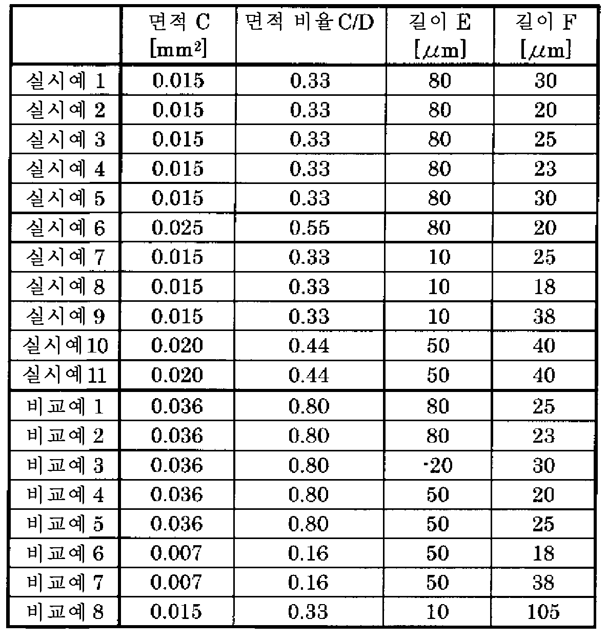
세라믹 기판으로서 판 두께가 0.635mm인 질화규소 기판(열전도율: 90W/mㆍK, 3점 굽힘 강도: 730MPa)과, 판 두께가 0.635mm인 질화알루미늄 기판(열전도율: 180W/mㆍK, 3점 굽힘 강도: 400MPa)과, 판 두께가 0.635mm인 산화알루미늄 기판(열전도율: 15W/mㆍK, 3점 굽힘 강도: 500MPa)을 준비하였다. 세라믹 기판의 형상은 세로 50mm×가로 30mm로 통일하였다.(Thermal conductivity: 90 W / m 占,, 3 point bending strength: 730 MPa) having a thickness of 0.635 mm and an aluminum nitride substrate having a plate thickness of 0.635 mm (thermal conductivity: 180 W / m 占,, three-point bending Strength: 400 MPa) and an aluminum oxide substrate (thermal conductivity: 15 W / m 占,, three-point bending strength: 500 MPa) having a plate thickness of 0.635 mm were prepared. The shape of the ceramic substrate was unified to be 50 mm long × 30 mm wide.
이어서, 표 1에 조성을 나타내는 활성 금속 땜납재를 제조하고, 페이스트화하여 세라믹 기판 상에 도포하였다. 활성 금속 땜납재 페이스트의 도포 두께는 표 1에 나타낸 바와 같다. 계속해서, 판 두께가 0.3mm인 동판(무산소 동판)을 준비하였다. 동판의 형상은 세로 45mm×가로 25mm로 통일하였다. 실시예 1 내지 9에서는 판 두께가 0.3mm인 동판을, 실시예 10 내지 11에서는 판 두께가 0.5mm인 동판을 사용하였다. 인쇄된 활성 금속 땜납재 페이스트 상에 동판을 배치하였다.Subsequently, an active metal solder material having a composition shown in Table 1 was prepared and paste was applied to a ceramic substrate. The coating thickness of the active metal solder paste is as shown in Table 1. Subsequently, a copper plate (oxygen-free copper plate) having a plate thickness of 0.3 mm was prepared. The shape of the copper plate was unified to 45 mm length x 25 mm width. In Examples 1 to 9, a copper plate having a plate thickness of 0.3 mm was used. In Examples 10 to 11, a copper plate having a plate thickness of 0.5 mm was used. A copper plate was placed on the printed active metal solder paste.
동판을 배치한 세라믹 기판을 진공 중에서 800 내지 840℃×20 내지 40분의 조건에서 가열함으로써, 세라믹 기판의 양면에 동판을 접합하였다. FeCl3 에칭액을 사용하여 표면측의 동판을 에칭함으로써, 도 4에 도시하는 2개의 회로 패턴을 형성하였다. 회로 패턴은 세로 20mm×가로 20mm의 패턴을 2mm의 간격을 두고 2개 형성한 구조로 하였다. 또한, 에칭 조건을 여러가지로 바꿈으로써, 동판의 단부를 표 2에 나타내는 조건을 충족하는 형상으로 가공하였다. 표 2에 나타내는 동판의 단부 형상은 구리 회로판 및 후면측 동판의 양쪽에 형성하였다.The ceramic substrate on which the copper plates were placed was heated in vacuum at 800 to 840 占 폚 for 20 to 40 minutes to join the copper plates to both surfaces of the ceramic substrate. FeCl 3 The copper plate on the front surface side was etched using an etching solution to form the two circuit patterns shown in Fig. The circuit pattern has a structure in which two patterns each having a length of 20 mm and a width of 20 mm are formed at intervals of 2 mm. Further, by changing the etching conditions in various ways, the end portions of the copper plate were processed into shapes satisfying the conditions shown in Table 2. [ The end shapes of the copper plates shown in Table 2 were formed on both the copper circuit board and the rear side copper plate.

실시예 1 내지 11 및 비교예 1 내지 8의 세라믹 구리 회로 기판에 대하여, 동판의 접합 강도, 내전압 불량률, TCT 특성, 화상 인식에 의한 위치 결정 정밀도를 조사하였다. 접합 강도는 박리 강도에 의해 측정하였다. 내전압 불량률은, N=20에서 표리 동판간에 10kV×1분간의 전압을 인가하였을 때의 관통 불량의 발생률(%)에 의해 평가하였다. 내전압 불량률은, 그것이 낮을수록 불량이 발생하지 않는 것을 의미한다.The bonding strength, the withstand voltage defect ratio, the TCT characteristics, and the positioning accuracy by image recognition were examined for the ceramic copper circuit boards of Examples 1 to 11 and Comparative Examples 1 to 8. The bonding strength was measured by peeling strength. The withstand voltage defect rate was evaluated by the occurrence rate (%) of the failure of penetration when a voltage of 10 kV x 1 minute was applied between copper plates at N = 20. The withstand voltage defect ratio means that no defects occur as the withstand voltage defect ratio becomes lower.
TCT 특성은, 이하에 나타내는 3가지 조건에 의해 평가하였다. 조건 1은 -40℃×30분 → 실온(25℃)×10분 → 125℃×30분 → 실온(25℃)×10분을 1사이클로 하였다. 조건 2는 -40℃×30분 → 실온(25℃)×10분 → 175℃×30분 → 실온(25℃)×10분을 1사이클로 하였다. 조건 3은 -50℃×30분 → 실온(25℃)×10분 → 250℃×30분 → 실온(25℃)×10분을 1사이클로 하였다. 각각 1000사이클 후의 세라믹 기판의 균열 유무를 건전율 η(%)로 조사하였다. 건전율 η(%)이란, 세라믹 구리 회로 기판의 동판의 접합 단부 주위에 형성되는 균열의 비율을 조사한 것이다. 동판의 접합 단부의 주위 길이를 100%라고 하였을 때, 균열이 발생하지 않은 비율을 측정한다. 건전율 η(%)가 100%라고 하는 것은, 균열이 발생한 것이 없었던 것을 의미한다. 건전율 η(%)가 0%라고 하는 것은, 모든 동판의 접합 단부의 주위 길이에 균열이 발생한 것을 의미한다. TCT는 시료수를 N=20으로 하여, 건전율 η(%)가 가장 큰 시료의 값을 나타낸다.The TCT characteristics were evaluated according to the following three conditions.
화상 인식에 의한 위치 결정 정밀도에 대해서는, 본더 마운터 장치에 의해 목적으로 하는 위치에 반도체 칩을 탑재할 수 있는지의 여부로 조사하였다. 위치 어긋남이 발생하지 않은 것을 「A」, 위치 어긋남이 발생한 것을 「B」로 하였다. 그들 결과를 표 3에 나타낸다.Regarding the positioning accuracy by image recognition, it was examined whether or not a semiconductor chip could be mounted at a desired position by the bonder mounting apparatus. &Quot; A " where no positional deviation occurred, and " B " The results are shown in Table 3.

표 3으로부터 알 수 있는 바와 같이, 실시예의 세라믹 구리 회로 기판은 모두 우수한 TCT 특성을 갖고 있었다. 본더 마운터 장치(CCD 카메라에 의한 화상 인식 타입)에 의한 위치 어긋남도 발생하지 않았다. 또한, 동판의 단부 형상을 개량하였기 때문에, 구리 회로판 상의 반도체 칩의 탑재 면적을 넓게 확보할 수 있다.As can be seen from Table 3, all of the ceramic copper circuit boards of the examples had excellent TCT characteristics. The positional deviation by the bonder mount device (image recognition type by CCD camera) did not occur. Further, since the shape of the end portion of the copper plate is improved, it is possible to secure a large mounting area of the semiconductor chip on the copper circuit board.
(실시예 12 내지 13)(Examples 12 to 13)
실시예 9의 세라믹 구리 회로 기판을 실시예 12, 실시예 9의 세라믹 구리 회로 기판의 동판 두께를 0.5mm로 바꾼 것을 실시예 13으로 하였다. 실시예 12 및 실시예 13의 세라믹 구리 회로 기판에 대하여, 조건 2(1사이클: -40℃×30분 → 실온(25℃)×10분 → 175℃×30분 → 실온(25℃)×10분)에서 TCT를 실시하여, 세라믹 기판에 균열이 발생하는 사이클수를 조사하였다. 그 결과를 표 4에 나타낸다.The ceramic copper circuit board of Example 9 was changed to the copper plate thickness of the ceramic copper circuit board of Example 12 and Example 9 by 0.5 mm. (1 cycle: -40 占 폚 for 30 minutes? Room temperature (25 占 폚) 占 10 minutes? 175 占 폚 占 30 minutes? Room temperature (25 占 폚) 占 10 占 10 minutes for the ceramic copper circuit substrates of Example 12 and Example 13 Minute), TCT was performed to investigate the number of cycles in which cracks occurred in the ceramic substrate. The results are shown in Table 4.

표 4로부터 알 수 있는 바와 같이, 실시예의 세라믹 구리 회로 기판은, 최대 온도가 170℃를 초과하는 TCT에 대해서도 6000사이클 이상의 내구성을 갖고 있다.As can be seen from Table 4, the ceramic copper circuit board of the embodiment has a durability of 6000 cycles or more even for a TCT whose maximum temperature exceeds 170 ° C.
(실시예 14 내지 18)(Examples 14 to 18)
세라믹 기판으로서 이하의 것을 준비하였다. 세라믹 기판(1)은 판 두께가 0.320mm인 질화규소 기판(열전도율: 93W/mㆍK, 3점 굽힘 강도: 700MPa)이다. 세라믹 기판(2)은 판 두께가 0.320mm인 질화규소 기판(열전도율: 100W/mㆍK, 3점 굽힘 강도: 600MPa)이다. 세라믹 기판(3)은 판 두께가 0.635mm인 질화알루미늄 기판(열전도율: 200W/mㆍK, 3점 굽힘 강도: 320MPa)이다. 세라믹 기판(4)은 판 두께가 0.635mm인 산화알루미늄 기판(열전도율: 12W/mㆍK, 3점 굽힘 강도: 400MPa)이다. 또한, 세라믹 기판의 형상은 세로 50mm×가로 30mm로 통일하였다.The following ceramic substrates were prepared. The
이어서, 표 5에 조성을 나타내는 활성 금속 땜납재를 제조하고, 페이스트화하여 세라믹 기판 상에 인쇄하여 도포하였다. 세로 45mm×가로 20mm×두께 0.3mm의 동판을 준비하였다. 활성 금속 땜납재 페이스트의 도포층 상에 동판을 배치하였다. 동판을 배치한 세라믹 기판을 진공 중에서 800 내지 840℃×20 내지 40분의 조건에서 가열함으로써, 세라믹 기판의 양면에 동판을 접합하였다. FeCl3 에칭액을 사용하여 표면측의 동판을 에칭하여, 도 4에 도시하는 2개의 회로 패턴을 형성하였다. 회로 패턴은 세로 20mm×가로 20mm의 패턴을 2mm의 간격을 두고 2개 형성한 구조로 하였다. 계속해서, 에칭 조건을 여러가지로 바꿈으로써, 동판의 단부를 표 6에 나타내는 조건을 충족하는 형상으로 가공하였다. 표 6에 나타내는 동판의 단부 형상은 구리 회로판 및 후면측 동판의 양쪽에 형성하였다.Subsequently, an active metal solder material having a composition shown in Table 5 was prepared and paste was printed and applied onto a ceramic substrate. A copper plate of 45 mm length x 20 mm width x 0.3 mm thickness was prepared. A copper plate was disposed on the application layer of the active metal solder paste. The ceramic substrate on which the copper plates were placed was heated in vacuum at 800 to 840 占 폚 for 20 to 40 minutes to join the copper plates to both surfaces of the ceramic substrate. The copper plate on the front surface side was etched using the FeCl 3 etching solution to form the two circuit patterns shown in Fig. The circuit pattern has a structure in which two patterns each having a length of 20 mm and a width of 20 mm are formed at intervals of 2 mm. Subsequently, by changing the etching conditions in various ways, the ends of the copper plate were processed into a shape satisfying the conditions shown in Table 6. The end portions of the copper plates shown in Table 6 were formed on both the copper circuit board and the rear side copper plate.


실시예 14 내지 18의 세라믹 구리 회로 기판에 대하여, 실시예 1과 마찬가지의 방법에 의해 접합 강도, 내전압 불량률, TCT 특성(조건 1, 조건 2, 조건 3), 위치 결정 정밀도를 측정하였다. 그들 결과를 표 7에 나타낸다. 표 7로부터 알 수 있는 바와 같이, 실시예의 세라믹 구리 회로 기판은 모두 우수한 특성을 갖고 있는 것이 확인되었다.With respect to the ceramic copper circuit boards of Examples 14 to 18, the bonding strength, the withstand voltage defect ratio, the TCT characteristics (

이어서, 조건 2(1사이클: -40℃×30분 → 실온(25℃)×10분 → 175℃×30분 → 실온(25℃)×10분)의 TCT를 실시하여, 세라믹 기판에 균열이 발생하는 사이클수를 조사하였다. 그 결과를 표 8에 나타낸다.Subsequently, TCT was performed under Condition 2 (1 cycle: -40 ° C × 30 minutes → room temperature (25 ° C.) × 10 minutes → 175 ° C. × 30 minutes → room temperature (25 ° C.) × 10 minutes) The number of cycles that occurred was investigated. The results are shown in Table 8.

표 8로부터 알 수 있는 바와 같이, 질화규소 기판을 사용한 실시예 14 내지 16은 모두 5000사이클 이상의 내구성을 갖고 있었다. 질화알루미늄 기판을 사용한 실시예 17과 산화알루미늄 기판을 사용한 실시예 18의 내구성은 1400 내지 1500사이클 정도이며, 실시예 14 내지 16에 비하여 떨어지기는 하지만, 종래의 질화알루미늄 기판이나 산화알루미늄 기판을 사용한 세라믹 구리 회로 기판에 비하여 우수한 TCT 특성을 갖는 것이 확인되었다. 실시예 14 내지 18의 결과로부터, 질화규소 기판을 사용함으로써, 세라믹 구리 회로 기판의 TCT 특성이 한층 더 향상되는 것을 알 수 있다.As can be seen from Table 8, all of Examples 14 to 16 using the silicon nitride substrate had durability over 5000 cycles. The durability of Example 17 using an aluminum nitride substrate and Example 18 using an aluminum oxide substrate is about 1400 to 1500 cycles and is lower than that of Examples 14 to 16. However, the conventional aluminum nitride substrate or ceramic substrate using an aluminum oxide substrate It was confirmed that TCT characteristics are superior to those of copper circuit boards. From the results of Examples 14 to 18, it can be seen that by using a silicon nitride substrate, the TCT characteristics of the ceramic copper circuit board are further improved.
또한, 본 발명의 몇 가지 실시 형태를 설명하였지만, 이들 실시 형태는 예로서 제시한 것이며, 발명의 범위를 한정하는 것은 의도하고 있지 않다. 이들 신규의 실시 형태는 그 밖의 다양한 형태로 실시할 수 있는 것이며, 발명의 요지를 일탈하지 않는 범위에서 다양한 생략, 치환, 변경을 행할 수 있다. 이들 실시 형태나 그 변형은 발명의 범위나 요지에 포함됨과 함께, 특허청구범위에 기재된 발명과 그 균등한 범위에 포함된다.Furthermore, although a few embodiments of the present invention have been described, these embodiments are presented as examples, and are not intended to limit the scope of the invention. These new embodiments can be implemented in various other forms, and various omissions, substitutions, and alterations can be made without departing from the gist of the invention. These embodiments and their modifications are included in the scope and spirit of the invention, and are included in the scope of the invention described in claims and their equivalents.
Claims (12)
Ti, Zr, Hf, Al 및 Nb로부터 선택되는 적어도 1종의 활성 금속 원소와 Ag, Cu, Sn, In 및 C로부터 선택되는 적어도 1종의 원소를 포함하는 제1 접합층을 개재하여, 상기 세라믹 기판의 제1 면에 접합된 제1 동판과,
Ti, Zr, Hf, Al 및 Nb로부터 선택되는 적어도 1종의 활성 금속 원소와 Ag, Cu, Sn, In 및 C로부터 선택되는 적어도 1종의 원소를 포함하는 제2 접합층을 개재하여, 상기 세라믹 기판의 제2 면에 접합된 제2 동판을 구비하며,
상기 제1 및 제2 동판의 단부의 단면에 있어서, 상기 동판과 상기 세라믹 기판의 접합 단부를 점 A, 상기 점 A로부터 상기 동판의 상면 내측을 향하여 상기 동판과 상기 세라믹 기판의 계면과 45°가 되는 방향으로 그은 직선과 상기 동판 상면이 교차하는 점을 점 B, 상기 점 A와 상기 점 B를 연결하는 직선 AB로부터 상기 동판의 외측 방향을 향하여 돌출되어 나오는 단면의 면적을 면적 C, 상기 직선 AB를 빗변으로 하는 직각삼각형에 상당하는 단면의 면적을 면적 D라고 하였을 때, 상기 제1 및 제2 동판의 단부는 상기 면적 D에 대한 상기 면적 C의 비율(C/D)이 0.2 이상 0.6 이하의 범위인 형상을 갖고,
상기 면적 C의 코너부에 상당하는 상기 제1 및 제2 동판의 상기 상면의 단부에는 각각 R부가 형성되어 있고, 또한 상기 R부의 상기 제1 및 제2 동판의 상방으로부터 본 길이 F가 100㎛ 이하인 것을 특징으로 하는 세라믹 구리 회로 기판.A ceramic substrate having a first surface and a second surface,
A first bonding layer containing at least one kind of active metal element selected from Ti, Zr, Hf, Al and Nb and at least one element selected from Ag, Cu, Sn, In and C, A first copper plate bonded to a first surface of the substrate;
And a second bonding layer comprising at least one kind of active metal element selected from Ti, Zr, Hf, Al and Nb and at least one element selected from Ag, Cu, Sn, In and C, And a second copper plate bonded to a second surface of the substrate,
A connecting end of the copper plate and the ceramic substrate is set at point A and a connecting point between the copper plate and the ceramic substrate is formed at an angle of 45 degrees from the point A to the inside of the upper surface of the copper plate, A point B where a straight line connecting the point A and the point B intersects the upper surface of the copper plate is defined as an area C and an area of the cross section protruding from the straight line AB connecting the point A and the point B toward the outward direction of the copper plate, (C / D) of the area C to the area D is not less than 0.2 and not more than 0.6, and the area of the end face of the first and second copper plates is not less than 0.2 Lt; / RTI >
Each of R portions is formed at an end portion of the upper surface of the first and second copper plates corresponding to the corner portion of the area C and the length F viewed from above of the first and second copper plates of the R portion is 100 mu m or less Wherein said ceramic copper circuit board is made of copper.
상기 세라믹 구리 회로 기판의 상기 제1 동판 상에 탑재된 반도체 칩을 구비하는 것을 특징으로 하는 반도체 장치.A ceramic copper circuit substrate according to claim 1;
And a semiconductor chip mounted on the first copper plate of the ceramic copper circuit board.
12. The semiconductor device according to claim 11, wherein the semiconductor chip comprises a SiC element.
Applications Claiming Priority (3)
| Application Number | Priority Date | Filing Date | Title |
|---|---|---|---|
| JPJP-P-2011-278945 | 2011-12-20 | ||
| JP2011278945 | 2011-12-20 | ||
| PCT/JP2012/008178 WO2013094213A1 (en) | 2011-12-20 | 2012-12-20 | Ceramic copper circuit board and semiconductor device employing same |
Publications (2)
| Publication Number | Publication Date |
|---|---|
| KR20140112029A true KR20140112029A (en) | 2014-09-22 |
| KR101659194B1 KR101659194B1 (en) | 2016-09-22 |
Family
ID=48668130
Family Applications (1)
| Application Number | Title | Priority Date | Filing Date |
|---|---|---|---|
| KR1020147019767A KR101659194B1 (en) | 2011-12-20 | 2012-12-20 | Ceramic copper circuit board and semiconductor device employing same |
Country Status (5)
| Country | Link |
|---|---|
| US (1) | US9357643B2 (en) |
| JP (3) | JP5976678B2 (en) |
| KR (1) | KR101659194B1 (en) |
| CN (1) | CN104011852B (en) |
| WO (1) | WO2013094213A1 (en) |
Cited By (2)
| Publication number | Priority date | Publication date | Assignee | Title |
|---|---|---|---|---|
| KR20190119000A (en) * | 2016-08-30 | 2019-10-21 | 주식회사 아모센스 | Ceramic board and manufacturing method thereof |
| US10515868B2 (en) | 2015-09-28 | 2019-12-24 | Kabushiki Kaisha Toshiba | Circuit substrate and semiconductor device |
Families Citing this family (47)
| Publication number | Priority date | Publication date | Assignee | Title |
|---|---|---|---|---|
| JP6056432B2 (en) * | 2012-12-06 | 2017-01-11 | 三菱マテリアル株式会社 | Power module substrate, power module substrate with heat sink, power module, power module substrate manufacturing method |
| CN105452195B (en) * | 2013-09-30 | 2018-01-02 | 三菱综合材料株式会社 | Cu ceramic joined articles, the manufacture method of Cu ceramic joined articles and power module substrate |
| JP6307386B2 (en) * | 2014-08-20 | 2018-04-04 | デンカ株式会社 | Ceramic circuit board |
| CN104409425B (en) * | 2014-11-13 | 2018-03-13 | 河北中瓷电子科技有限公司 | High heat conduction silicon nitride ceramics copper-clad plate and preparation method thereof |
| WO2016125635A1 (en) | 2015-02-02 | 2016-08-11 | 株式会社東芝 | Silicon nitride circuit substrate and electronic component module using same |
| DE102015110607A1 (en) * | 2015-07-01 | 2017-01-05 | Epcos Ag | Method for producing an electrical component |
| CN107851617B (en) * | 2015-07-09 | 2021-04-30 | 株式会社东芝 | Ceramic metal circuit board and semiconductor device using the same |
| US10160690B2 (en) * | 2015-09-28 | 2018-12-25 | Kabushiki Kaisha Toshiba | Silicon nitride circuit board and semiconductor module using the same |
| CN107295755A (en) * | 2016-04-13 | 2017-10-24 | 讯芯电子科技(中山)有限公司 | Cover the manufacture method of copper ceramic substrate |
| CN109155291B (en) * | 2016-05-19 | 2022-05-03 | 三菱综合材料株式会社 | Substrate for power module |
| CN109417854B (en) * | 2016-06-21 | 2021-04-27 | 阿莫善斯有限公司 | Ceramic substrate and method for manufacturing same |
| WO2018021473A1 (en) * | 2016-07-28 | 2018-02-01 | 株式会社 東芝 | Circuit board and semiconductor module |
| CN114478045B (en) * | 2016-07-28 | 2023-08-15 | 株式会社东芝 | Bonded body, circuit board, and semiconductor device |
| US10104759B2 (en) * | 2016-11-29 | 2018-10-16 | Nxp Usa, Inc. | Microelectronic modules with sinter-bonded heat dissipation structures and methods for the fabrication thereof |
| JP6732239B2 (en) * | 2016-12-22 | 2020-07-29 | 株式会社Nsc | POWER MODULE BOARD AND ITS PRODUCTION METHOD |
| JP7204637B2 (en) | 2017-03-23 | 2023-01-16 | 株式会社東芝 | CERAMIC METAL CIRCUIT BOARD AND SEMICONDUCTOR DEVICE USING SAME |
| CN115295523A (en) | 2017-03-30 | 2022-11-04 | 株式会社东芝 | Ceramic copper circuit board and semiconductor device using the same |
| DE102017107116A1 (en) * | 2017-04-03 | 2018-10-04 | Semikron Elektronik Gmbh & Co. Kg | Substrate having a cornered first metal layer region |
| WO2018207396A1 (en) * | 2017-05-11 | 2018-11-15 | 住友電気工業株式会社 | Semiconductor device |
| CN110709369A (en) * | 2017-05-30 | 2020-01-17 | 电化株式会社 | Ceramic circuit board and module using the same |
| JP7369508B2 (en) * | 2017-08-04 | 2023-10-26 | デンカ株式会社 | ceramic circuit board |
| JP7299671B2 (en) * | 2017-08-04 | 2023-06-28 | デンカ株式会社 | ceramic circuit board |
| JP6955943B2 (en) * | 2017-09-26 | 2021-10-27 | 京セラ株式会社 | Wiring boards and electronic devices |
| JP7298988B2 (en) * | 2017-09-28 | 2023-06-27 | デンカ株式会社 | Ceramic circuit board and its manufacturing method |
| JP7299672B2 (en) * | 2017-09-28 | 2023-06-28 | デンカ株式会社 | Ceramic circuit board and its manufacturing method |
| JP7230432B2 (en) * | 2017-11-02 | 2023-03-01 | 三菱マテリアル株式会社 | Joined body and insulating circuit board |
| CN108155103A (en) * | 2017-12-26 | 2018-06-12 | 天津荣事顺发电子有限公司 | A kind of aluminium nitride ceramic copper-clad substrate and preparation method thereof |
| JP6939596B2 (en) * | 2018-01-24 | 2021-09-22 | 三菱マテリアル株式会社 | Manufacturing method of substrate for power module and ceramics-copper joint |
| JP7002993B2 (en) * | 2018-05-10 | 2022-01-20 | 株式会社 日立パワーデバイス | Power semiconductor module |
| EP3796761A4 (en) * | 2018-05-16 | 2022-01-26 | Kabushiki Kaisha Toshiba | Ceramic copper circuit board and method for producing same |
| WO2020044594A1 (en) * | 2018-08-28 | 2020-03-05 | 三菱マテリアル株式会社 | Copper/ceramic bonded body, insulation circuit board, method for producing copper/ceramic bonded body, and method for manufacturing insulation circuit board |
| WO2020067427A1 (en) * | 2018-09-27 | 2020-04-02 | デンカ株式会社 | Bonded substrate, metal circuit board, and circuit board |
| JP7147502B2 (en) | 2018-11-19 | 2022-10-05 | 三菱電機株式会社 | Semiconductor device, power conversion device, and method for manufacturing semiconductor device |
| JP7176397B2 (en) * | 2018-12-21 | 2022-11-22 | 株式会社デンソー | Semiconductor device and its manufacturing method |
| EP3941166A4 (en) * | 2019-03-14 | 2022-11-09 | NGK Insulators, Ltd. | Bonded substrate |
| WO2020208698A1 (en) * | 2019-04-09 | 2020-10-15 | 日本碍子株式会社 | Bonded substrate and method for manufacturing bonded substrate |
| JPWO2020209175A1 (en) * | 2019-04-11 | 2020-10-15 | ||
| EP4006002A4 (en) * | 2019-07-23 | 2023-09-06 | NGK Insulators, Ltd. | Bonded substrate, and method for manufacturing bonded substrate |
| WO2021044854A1 (en) * | 2019-09-02 | 2021-03-11 | 株式会社 東芝 | Joined body, circuit board, and semiconductor device |
| KR20220066051A (en) | 2019-09-20 | 2022-05-23 | 덴카 주식회사 | Circuit board and module having same |
| JPWO2021200866A1 (en) * | 2020-03-30 | 2021-10-07 | ||
| JP7314208B2 (en) | 2020-07-02 | 2023-07-25 | レオン自動機株式会社 | Dispensing device for food materials |
| EP4197990A1 (en) * | 2020-08-12 | 2023-06-21 | Tokuyama Corporation | Laminate for circuit board |
| JPWO2022075409A1 (en) * | 2020-10-07 | 2022-04-14 | ||
| CN116018884A (en) * | 2020-10-20 | 2023-04-25 | 株式会社东芝 | Bonded body, ceramic circuit board using the same, and semiconductor device |
| WO2022138750A1 (en) * | 2020-12-24 | 2022-06-30 | 株式会社 東芝 | Insulation circuit board and semiconductor device using same |
| DE102022113636A1 (en) | 2022-05-31 | 2023-11-30 | Rolls-Royce Deutschland Ltd & Co Kg | Electrical module |
Citations (6)
| Publication number | Priority date | Publication date | Assignee | Title |
|---|---|---|---|---|
| JPH04346151A (en) | 1991-05-24 | 1992-12-02 | Canon Inc | Data processor |
| JPH05304350A (en) * | 1992-04-27 | 1993-11-16 | Mitsubishi Electric Corp | Printed wiring board and its production |
| JPH11340598A (en) | 1998-05-22 | 1999-12-10 | Toshiba Corp | Ceramic circuit board |
| JP2002232090A (en) * | 2001-01-30 | 2002-08-16 | Kyocera Corp | Ceramic circuit board |
| JP2004314161A (en) * | 2003-04-21 | 2004-11-11 | Hitachi Metals Ltd | Brazing material for ceramic substrates, and ceramic circuit board using the same |
| WO2011034075A1 (en) | 2009-09-15 | 2011-03-24 | 株式会社 東芝 | Ceramic circuit board and process for producing same |
Family Cites Families (38)
| Publication number | Priority date | Publication date | Assignee | Title |
|---|---|---|---|---|
| US4657825A (en) * | 1984-12-24 | 1987-04-14 | Ngk Spark Plug Co., Ltd. | Electronic component using a silicon carbide substrate and a method of making it |
| US5098494A (en) * | 1989-05-23 | 1992-03-24 | Mcnc | Bonding of ceramic parts |
| US5328751A (en) * | 1991-07-12 | 1994-07-12 | Kabushiki Kaisha Toshiba | Ceramic circuit board with a curved lead terminal |
| JPH07202063A (en) * | 1993-12-28 | 1995-08-04 | Toshiba Corp | Ceramic circuit board |
| JP4077888B2 (en) * | 1995-07-21 | 2008-04-23 | 株式会社東芝 | Ceramic circuit board |
| JPH104156A (en) * | 1996-06-14 | 1998-01-06 | Mitsubishi Electric Corp | Insulating substrate for semiconductor device and the semiconductor device |
| US6232657B1 (en) * | 1996-08-20 | 2001-05-15 | Kabushiki Kaisha Toshiba | Silicon nitride circuit board and semiconductor module |
| JP3512977B2 (en) * | 1996-08-27 | 2004-03-31 | 同和鉱業株式会社 | High reliability semiconductor substrate |
| KR100371974B1 (en) * | 1997-05-26 | 2003-02-17 | 스미토모덴키고교가부시키가이샤 | Copper circuit junction substrate and method of producing the same |
| JP4346151B2 (en) | 1998-05-12 | 2009-10-21 | 株式会社東芝 | High thermal conductivity sintered silicon nitride, circuit board and integrated circuit using the same |
| JP4334054B2 (en) * | 1999-03-26 | 2009-09-16 | 株式会社東芝 | Ceramic circuit board |
| JP4649027B2 (en) * | 1999-09-28 | 2011-03-09 | 株式会社東芝 | Ceramic circuit board |
| JP5038565B2 (en) * | 2000-09-22 | 2012-10-03 | 株式会社東芝 | Ceramic circuit board and manufacturing method thereof |
| US6613443B2 (en) * | 2000-10-27 | 2003-09-02 | Kabushiki Kaisha Toshiba | Silicon nitride ceramic substrate, silicon nitride ceramic circuit board using the substrate, and method of manufacturing the substrate |
| US6756672B1 (en) * | 2001-02-06 | 2004-06-29 | Advanced Micro Devices, Inc. | Use of sic for preventing copper contamination of low-k dielectric layers |
| US6663787B1 (en) * | 2001-02-06 | 2003-12-16 | Advanced Micro Devices, Inc. | Use of ta/tan for preventing copper contamination of low-k dielectric layers |
| US6677679B1 (en) * | 2001-02-06 | 2004-01-13 | Advanced Micro Devices, Inc. | Use of SiO2/Sin for preventing copper contamination of low-k dielectric layers |
| US6576982B1 (en) * | 2001-02-06 | 2003-06-10 | Advanced Micro Devices, Inc. | Use of sion for preventing copper contamination of dielectric layer |
| US6577009B1 (en) * | 2001-02-06 | 2003-06-10 | Advanced Micro Devices, Inc. | Use of sic for preventing copper contamination of dielectric layer |
| US6689684B1 (en) * | 2001-02-15 | 2004-02-10 | Advanced Micro Devices, Inc. | Cu damascene interconnections using barrier/capping layer |
| US7038320B1 (en) * | 2001-02-20 | 2006-05-02 | Advanced Micro Devices, Inc. | Single damascene integration scheme for preventing copper contamination of dielectric layer |
| US6586842B1 (en) * | 2001-02-28 | 2003-07-01 | Advanced Micro Devices, Inc. | Dual damascene integration scheme for preventing copper contamination of dielectric layer |
| JP4434545B2 (en) * | 2001-03-01 | 2010-03-17 | Dowaホールディングス株式会社 | Insulating substrate for semiconductor mounting and power module |
| DE60226111T2 (en) * | 2001-03-02 | 2009-05-28 | Panasonic Corp., Kadoma | DIELECTRIC FILTER AND ANTENNA VARIETIES |
| US6566242B1 (en) * | 2001-03-23 | 2003-05-20 | International Business Machines Corporation | Dual damascene copper interconnect to a damascene tungsten wiring level |
| JP2004172182A (en) * | 2002-11-18 | 2004-06-17 | Denki Kagaku Kogyo Kk | Circuit board and its manufacturing method |
| US6790758B2 (en) * | 2002-11-25 | 2004-09-14 | Silicon Integrated Systems Corp. | Method for fabricating conductive bumps and substrate with metal bumps for flip chip packaging |
| JP4664816B2 (en) * | 2003-09-25 | 2011-04-06 | 株式会社東芝 | Ceramic circuit board, manufacturing method thereof and power module |
| JP4696532B2 (en) * | 2004-05-20 | 2011-06-08 | 株式会社デンソー | Power composite integrated semiconductor device and manufacturing method thereof |
| JPWO2007105361A1 (en) * | 2006-03-08 | 2009-07-30 | 株式会社東芝 | Electronic component module |
| US8518554B2 (en) * | 2006-07-04 | 2013-08-27 | Kabushiki Kaisha Toshiba | Ceramic metal composite and semiconductor device using the same |
| US20090278233A1 (en) * | 2007-07-26 | 2009-11-12 | Pinnington Thomas Henry | Bonded intermediate substrate and method of making same |
| US9147812B2 (en) * | 2008-06-24 | 2015-09-29 | Cree, Inc. | Methods of assembly for a semiconductor light emitting device package |
| JP5319463B2 (en) * | 2009-09-03 | 2013-10-16 | 株式会社東芝 | Silicon nitride substrate with improved positioning and semiconductor device using the same |
| DE102009045181B4 (en) * | 2009-09-30 | 2020-07-09 | Infineon Technologies Ag | Power semiconductor module |
| JP5133960B2 (en) * | 2009-10-22 | 2013-01-30 | 電気化学工業株式会社 | Circuit board for semiconductor mounting and manufacturing method thereof |
| JP5551920B2 (en) * | 2009-11-24 | 2014-07-16 | イビデン株式会社 | Semiconductor device and manufacturing method thereof |
| JP5266508B2 (en) * | 2011-06-17 | 2013-08-21 | Dowaメタルテック株式会社 | Metal-ceramic bonding substrate |
-
2012
- 2012-12-20 CN CN201280063176.0A patent/CN104011852B/en active Active
- 2012-12-20 JP JP2013550130A patent/JP5976678B2/en active Active
- 2012-12-20 WO PCT/JP2012/008178 patent/WO2013094213A1/en active Application Filing
- 2012-12-20 KR KR1020147019767A patent/KR101659194B1/en active IP Right Grant
-
2014
- 2014-06-16 US US14/305,779 patent/US9357643B2/en active Active
-
2016
- 2016-04-25 JP JP2016086977A patent/JP6125691B2/en active Active
-
2017
- 2017-03-28 JP JP2017062986A patent/JP2017130686A/en active Pending
Patent Citations (6)
| Publication number | Priority date | Publication date | Assignee | Title |
|---|---|---|---|---|
| JPH04346151A (en) | 1991-05-24 | 1992-12-02 | Canon Inc | Data processor |
| JPH05304350A (en) * | 1992-04-27 | 1993-11-16 | Mitsubishi Electric Corp | Printed wiring board and its production |
| JPH11340598A (en) | 1998-05-22 | 1999-12-10 | Toshiba Corp | Ceramic circuit board |
| JP2002232090A (en) * | 2001-01-30 | 2002-08-16 | Kyocera Corp | Ceramic circuit board |
| JP2004314161A (en) * | 2003-04-21 | 2004-11-11 | Hitachi Metals Ltd | Brazing material for ceramic substrates, and ceramic circuit board using the same |
| WO2011034075A1 (en) | 2009-09-15 | 2011-03-24 | 株式会社 東芝 | Ceramic circuit board and process for producing same |
Cited By (3)
| Publication number | Priority date | Publication date | Assignee | Title |
|---|---|---|---|---|
| US10515868B2 (en) | 2015-09-28 | 2019-12-24 | Kabushiki Kaisha Toshiba | Circuit substrate and semiconductor device |
| US10790214B2 (en) | 2015-09-28 | 2020-09-29 | Kabushiki Kaisha Toshiba | Circuit substrate and semiconductor device |
| KR20190119000A (en) * | 2016-08-30 | 2019-10-21 | 주식회사 아모센스 | Ceramic board and manufacturing method thereof |
Also Published As
| Publication number | Publication date |
|---|---|
| JP2017130686A (en) | 2017-07-27 |
| US20140291699A1 (en) | 2014-10-02 |
| KR101659194B1 (en) | 2016-09-22 |
| US9357643B2 (en) | 2016-05-31 |
| CN104011852A (en) | 2014-08-27 |
| JP5976678B2 (en) | 2016-08-24 |
| CN104011852B (en) | 2016-12-21 |
| JPWO2013094213A1 (en) | 2015-04-27 |
| WO2013094213A1 (en) | 2013-06-27 |
| JP6125691B2 (en) | 2017-05-10 |
| JP2016174165A (en) | 2016-09-29 |
Similar Documents
| Publication | Publication Date | Title |
|---|---|---|
| KR101659194B1 (en) | Ceramic copper circuit board and semiconductor device employing same | |
| JP5598522B2 (en) | Circuit board, semiconductor module using the same, and circuit board manufacturing method | |
| CN107004643B (en) | Circuit substrate and electronic device | |
| JP5991103B2 (en) | Power module substrate with heat sink, power module with heat sink, and method for manufacturing power module substrate with heat sink | |
| JP2014060215A (en) | Substrate for power module with heat sink, power module with heat sink and manufacturing method of substrate for power module with heat sink | |
| JP2013211546A (en) | Ceramic-copper assembly and manufacturing method of the same | |
| TW201448056A (en) | Power module | |
| JP2016051778A (en) | Metal-ceramic bonded substrate | |
| EP3761764A1 (en) | Insulating circuit board | |
| KR102479866B1 (en) | Ceramic circuit board and its manufacturing method | |
| JP4360847B2 (en) | Ceramic circuit board, heat dissipation module, and semiconductor device | |
| JP6870767B2 (en) | Copper / ceramic joints and insulated circuit boards | |
| JP6259625B2 (en) | Bonding structure of insulating substrate and cooler, manufacturing method thereof, power semiconductor module, and manufacturing method thereof | |
| JP2023086688A (en) | Copper/ceramic jointed body and insulated circuit board | |
| JP2004055576A (en) | Circuit board and power module using it | |
| JP3779074B2 (en) | Ceramic circuit board and power module using it | |
| JP3794454B2 (en) | Nitride ceramic substrate | |
| KR102409815B1 (en) | Copper/ceramic bonded body, insulated circuit board, and copper/ceramic bonded body manufacturing method, and insulated circuit board manufacturing method | |
| JP2018046106A (en) | Copper/titanium/aluminum conjugate, insulation circuit board, insulation circuit board with heat sink, power module, led module, and electro-thermal module | |
| JP6614256B2 (en) | Insulated circuit board | |
| JP2011067849A (en) | Brazing filler metal, and heat radiation base body joined by using the same | |
| JP2021031315A (en) | Copper/ceramic joint, insulated circuit board, copper/ceramic joint producing method, insulated circuit board producing method | |
| KR102363709B1 (en) | Copper/Titanium/Aluminum bonding body, insulated circuit board, insulated circuit board with heatsink attached, power module, LED module, thermoelectric module | |
| WO2023106226A1 (en) | Copper/ceramic joined body and insulated circuit board | |
| JP2000049425A (en) | Ceramics circuit board, its manufacture and power module using the same |
Legal Events
| Date | Code | Title | Description |
|---|---|---|---|
| A201 | Request for examination | ||
| E902 | Notification of reason for refusal | ||
| AMND | Amendment | ||
| E601 | Decision to refuse application | ||
| AMND | Amendment | ||
| E902 | Notification of reason for refusal | ||
| AMND | Amendment | ||
| X701 | Decision to grant (after re-examination) |