KR20140058557A - Semiconductor package resin composition and usage method thereof - Google Patents
Semiconductor package resin composition and usage method thereof Download PDFInfo
- Publication number
- KR20140058557A KR20140058557A KR1020147003608A KR20147003608A KR20140058557A KR 20140058557 A KR20140058557 A KR 20140058557A KR 1020147003608 A KR1020147003608 A KR 1020147003608A KR 20147003608 A KR20147003608 A KR 20147003608A KR 20140058557 A KR20140058557 A KR 20140058557A
- Authority
- KR
- South Korea
- Prior art keywords
- semiconductor package
- resin composition
- package resin
- substrate
- particles
- Prior art date
Links
Images


Classifications
-
- H—ELECTRICITY
- H01—ELECTRIC ELEMENTS
- H01L—SEMICONDUCTOR DEVICES NOT COVERED BY CLASS H10
- H01L23/00—Details of semiconductor or other solid state devices
- H01L23/28—Encapsulations, e.g. encapsulating layers, coatings, e.g. for protection
- H01L23/29—Encapsulations, e.g. encapsulating layers, coatings, e.g. for protection characterised by the material, e.g. carbon
- H01L23/293—Organic, e.g. plastic
- H01L23/296—Organo-silicon compounds
-
- C—CHEMISTRY; METALLURGY
- C08—ORGANIC MACROMOLECULAR COMPOUNDS; THEIR PREPARATION OR CHEMICAL WORKING-UP; COMPOSITIONS BASED THEREON
- C08L—COMPOSITIONS OF MACROMOLECULAR COMPOUNDS
- C08L63/00—Compositions of epoxy resins; Compositions of derivatives of epoxy resins
-
- C—CHEMISTRY; METALLURGY
- C08—ORGANIC MACROMOLECULAR COMPOUNDS; THEIR PREPARATION OR CHEMICAL WORKING-UP; COMPOSITIONS BASED THEREON
- C08K—Use of inorganic or non-macromolecular organic substances as compounding ingredients
- C08K3/00—Use of inorganic substances as compounding ingredients
- C08K3/34—Silicon-containing compounds
- C08K3/36—Silica
-
- C—CHEMISTRY; METALLURGY
- C08—ORGANIC MACROMOLECULAR COMPOUNDS; THEIR PREPARATION OR CHEMICAL WORKING-UP; COMPOSITIONS BASED THEREON
- C08K—Use of inorganic or non-macromolecular organic substances as compounding ingredients
- C08K9/00—Use of pretreated ingredients
- C08K9/04—Ingredients treated with organic substances
- C08K9/06—Ingredients treated with organic substances with silicon-containing compounds
-
- H—ELECTRICITY
- H01—ELECTRIC ELEMENTS
- H01L—SEMICONDUCTOR DEVICES NOT COVERED BY CLASS H10
- H01L21/00—Processes or apparatus adapted for the manufacture or treatment of semiconductor or solid state devices or of parts thereof
- H01L21/02—Manufacture or treatment of semiconductor devices or of parts thereof
- H01L21/04—Manufacture or treatment of semiconductor devices or of parts thereof the devices having at least one potential-jump barrier or surface barrier, e.g. PN junction, depletion layer or carrier concentration layer
- H01L21/50—Assembly of semiconductor devices using processes or apparatus not provided for in a single one of the subgroups H01L21/06 - H01L21/326, e.g. sealing of a cap to a base of a container
- H01L21/56—Encapsulations, e.g. encapsulation layers, coatings
- H01L21/563—Encapsulation of active face of flip-chip device, e.g. underfilling or underencapsulation of flip-chip, encapsulation preform on chip or mounting substrate
-
- H—ELECTRICITY
- H01—ELECTRIC ELEMENTS
- H01L—SEMICONDUCTOR DEVICES NOT COVERED BY CLASS H10
- H01L23/00—Details of semiconductor or other solid state devices
- H01L23/02—Containers; Seals
- H01L23/10—Containers; Seals characterised by the material or arrangement of seals between parts, e.g. between cap and base of the container or between leads and walls of the container
-
- H—ELECTRICITY
- H01—ELECTRIC ELEMENTS
- H01L—SEMICONDUCTOR DEVICES NOT COVERED BY CLASS H10
- H01L23/00—Details of semiconductor or other solid state devices
- H01L23/28—Encapsulations, e.g. encapsulating layers, coatings, e.g. for protection
- H01L23/29—Encapsulations, e.g. encapsulating layers, coatings, e.g. for protection characterised by the material, e.g. carbon
- H01L23/293—Organic, e.g. plastic
- H01L23/295—Organic, e.g. plastic containing a filler
-
- H—ELECTRICITY
- H01—ELECTRIC ELEMENTS
- H01L—SEMICONDUCTOR DEVICES NOT COVERED BY CLASS H10
- H01L2224/00—Indexing scheme for arrangements for connecting or disconnecting semiconductor or solid-state bodies and methods related thereto as covered by H01L24/00
- H01L2224/01—Means for bonding being attached to, or being formed on, the surface to be connected, e.g. chip-to-package, die-attach, "first-level" interconnects; Manufacturing methods related thereto
- H01L2224/10—Bump connectors; Manufacturing methods related thereto
- H01L2224/15—Structure, shape, material or disposition of the bump connectors after the connecting process
- H01L2224/16—Structure, shape, material or disposition of the bump connectors after the connecting process of an individual bump connector
- H01L2224/161—Disposition
- H01L2224/16151—Disposition the bump connector connecting between a semiconductor or solid-state body and an item not being a semiconductor or solid-state body, e.g. chip-to-substrate, chip-to-passive
- H01L2224/16221—Disposition the bump connector connecting between a semiconductor or solid-state body and an item not being a semiconductor or solid-state body, e.g. chip-to-substrate, chip-to-passive the body and the item being stacked
- H01L2224/16225—Disposition the bump connector connecting between a semiconductor or solid-state body and an item not being a semiconductor or solid-state body, e.g. chip-to-substrate, chip-to-passive the body and the item being stacked the item being non-metallic, e.g. insulating substrate with or without metallisation
-
- H—ELECTRICITY
- H01—ELECTRIC ELEMENTS
- H01L—SEMICONDUCTOR DEVICES NOT COVERED BY CLASS H10
- H01L2224/00—Indexing scheme for arrangements for connecting or disconnecting semiconductor or solid-state bodies and methods related thereto as covered by H01L24/00
- H01L2224/01—Means for bonding being attached to, or being formed on, the surface to be connected, e.g. chip-to-package, die-attach, "first-level" interconnects; Manufacturing methods related thereto
- H01L2224/26—Layer connectors, e.g. plate connectors, solder or adhesive layers; Manufacturing methods related thereto
- H01L2224/31—Structure, shape, material or disposition of the layer connectors after the connecting process
- H01L2224/32—Structure, shape, material or disposition of the layer connectors after the connecting process of an individual layer connector
- H01L2224/321—Disposition
- H01L2224/32135—Disposition the layer connector connecting between different semiconductor or solid-state bodies, i.e. chip-to-chip
- H01L2224/32145—Disposition the layer connector connecting between different semiconductor or solid-state bodies, i.e. chip-to-chip the bodies being stacked
-
- H—ELECTRICITY
- H01—ELECTRIC ELEMENTS
- H01L—SEMICONDUCTOR DEVICES NOT COVERED BY CLASS H10
- H01L2224/00—Indexing scheme for arrangements for connecting or disconnecting semiconductor or solid-state bodies and methods related thereto as covered by H01L24/00
- H01L2224/01—Means for bonding being attached to, or being formed on, the surface to be connected, e.g. chip-to-package, die-attach, "first-level" interconnects; Manufacturing methods related thereto
- H01L2224/26—Layer connectors, e.g. plate connectors, solder or adhesive layers; Manufacturing methods related thereto
- H01L2224/31—Structure, shape, material or disposition of the layer connectors after the connecting process
- H01L2224/32—Structure, shape, material or disposition of the layer connectors after the connecting process of an individual layer connector
- H01L2224/321—Disposition
- H01L2224/32151—Disposition the layer connector connecting between a semiconductor or solid-state body and an item not being a semiconductor or solid-state body, e.g. chip-to-substrate, chip-to-passive
- H01L2224/32221—Disposition the layer connector connecting between a semiconductor or solid-state body and an item not being a semiconductor or solid-state body, e.g. chip-to-substrate, chip-to-passive the body and the item being stacked
- H01L2224/32225—Disposition the layer connector connecting between a semiconductor or solid-state body and an item not being a semiconductor or solid-state body, e.g. chip-to-substrate, chip-to-passive the body and the item being stacked the item being non-metallic, e.g. insulating substrate with or without metallisation
-
- H—ELECTRICITY
- H01—ELECTRIC ELEMENTS
- H01L—SEMICONDUCTOR DEVICES NOT COVERED BY CLASS H10
- H01L2224/00—Indexing scheme for arrangements for connecting or disconnecting semiconductor or solid-state bodies and methods related thereto as covered by H01L24/00
- H01L2224/01—Means for bonding being attached to, or being formed on, the surface to be connected, e.g. chip-to-package, die-attach, "first-level" interconnects; Manufacturing methods related thereto
- H01L2224/42—Wire connectors; Manufacturing methods related thereto
- H01L2224/47—Structure, shape, material or disposition of the wire connectors after the connecting process
- H01L2224/48—Structure, shape, material or disposition of the wire connectors after the connecting process of an individual wire connector
- H01L2224/4805—Shape
- H01L2224/4809—Loop shape
- H01L2224/48091—Arched
-
- H—ELECTRICITY
- H01—ELECTRIC ELEMENTS
- H01L—SEMICONDUCTOR DEVICES NOT COVERED BY CLASS H10
- H01L2224/00—Indexing scheme for arrangements for connecting or disconnecting semiconductor or solid-state bodies and methods related thereto as covered by H01L24/00
- H01L2224/01—Means for bonding being attached to, or being formed on, the surface to be connected, e.g. chip-to-package, die-attach, "first-level" interconnects; Manufacturing methods related thereto
- H01L2224/42—Wire connectors; Manufacturing methods related thereto
- H01L2224/47—Structure, shape, material or disposition of the wire connectors after the connecting process
- H01L2224/48—Structure, shape, material or disposition of the wire connectors after the connecting process of an individual wire connector
- H01L2224/481—Disposition
- H01L2224/48151—Connecting between a semiconductor or solid-state body and an item not being a semiconductor or solid-state body, e.g. chip-to-substrate, chip-to-passive
- H01L2224/48221—Connecting between a semiconductor or solid-state body and an item not being a semiconductor or solid-state body, e.g. chip-to-substrate, chip-to-passive the body and the item being stacked
- H01L2224/48225—Connecting between a semiconductor or solid-state body and an item not being a semiconductor or solid-state body, e.g. chip-to-substrate, chip-to-passive the body and the item being stacked the item being non-metallic, e.g. insulating substrate with or without metallisation
- H01L2224/48227—Connecting between a semiconductor or solid-state body and an item not being a semiconductor or solid-state body, e.g. chip-to-substrate, chip-to-passive the body and the item being stacked the item being non-metallic, e.g. insulating substrate with or without metallisation connecting the wire to a bond pad of the item
-
- H—ELECTRICITY
- H01—ELECTRIC ELEMENTS
- H01L—SEMICONDUCTOR DEVICES NOT COVERED BY CLASS H10
- H01L2224/00—Indexing scheme for arrangements for connecting or disconnecting semiconductor or solid-state bodies and methods related thereto as covered by H01L24/00
- H01L2224/73—Means for bonding being of different types provided for in two or more of groups H01L2224/10, H01L2224/18, H01L2224/26, H01L2224/34, H01L2224/42, H01L2224/50, H01L2224/63, H01L2224/71
- H01L2224/732—Location after the connecting process
- H01L2224/73201—Location after the connecting process on the same surface
- H01L2224/73203—Bump and layer connectors
- H01L2224/73204—Bump and layer connectors the bump connector being embedded into the layer connector
-
- H—ELECTRICITY
- H01—ELECTRIC ELEMENTS
- H01L—SEMICONDUCTOR DEVICES NOT COVERED BY CLASS H10
- H01L2224/00—Indexing scheme for arrangements for connecting or disconnecting semiconductor or solid-state bodies and methods related thereto as covered by H01L24/00
- H01L2224/73—Means for bonding being of different types provided for in two or more of groups H01L2224/10, H01L2224/18, H01L2224/26, H01L2224/34, H01L2224/42, H01L2224/50, H01L2224/63, H01L2224/71
- H01L2224/732—Location after the connecting process
- H01L2224/73251—Location after the connecting process on different surfaces
- H01L2224/73253—Bump and layer connectors
-
- H—ELECTRICITY
- H01—ELECTRIC ELEMENTS
- H01L—SEMICONDUCTOR DEVICES NOT COVERED BY CLASS H10
- H01L2224/00—Indexing scheme for arrangements for connecting or disconnecting semiconductor or solid-state bodies and methods related thereto as covered by H01L24/00
- H01L2224/73—Means for bonding being of different types provided for in two or more of groups H01L2224/10, H01L2224/18, H01L2224/26, H01L2224/34, H01L2224/42, H01L2224/50, H01L2224/63, H01L2224/71
- H01L2224/732—Location after the connecting process
- H01L2224/73251—Location after the connecting process on different surfaces
- H01L2224/73265—Layer and wire connectors
-
- H—ELECTRICITY
- H01—ELECTRIC ELEMENTS
- H01L—SEMICONDUCTOR DEVICES NOT COVERED BY CLASS H10
- H01L2224/00—Indexing scheme for arrangements for connecting or disconnecting semiconductor or solid-state bodies and methods related thereto as covered by H01L24/00
- H01L2224/91—Methods for connecting semiconductor or solid state bodies including different methods provided for in two or more of groups H01L2224/80 - H01L2224/90
- H01L2224/92—Specific sequence of method steps
- H01L2224/921—Connecting a surface with connectors of different types
- H01L2224/9212—Sequential connecting processes
- H01L2224/92122—Sequential connecting processes the first connecting process involving a bump connector
- H01L2224/92125—Sequential connecting processes the first connecting process involving a bump connector the second connecting process involving a layer connector
-
- H—ELECTRICITY
- H01—ELECTRIC ELEMENTS
- H01L—SEMICONDUCTOR DEVICES NOT COVERED BY CLASS H10
- H01L2924/00—Indexing scheme for arrangements or methods for connecting or disconnecting semiconductor or solid-state bodies as covered by H01L24/00
- H01L2924/10—Details of semiconductor or other solid state devices to be connected
- H01L2924/11—Device type
- H01L2924/12—Passive devices, e.g. 2 terminal devices
- H01L2924/1204—Optical Diode
- H01L2924/12044—OLED
-
- H—ELECTRICITY
- H01—ELECTRIC ELEMENTS
- H01L—SEMICONDUCTOR DEVICES NOT COVERED BY CLASS H10
- H01L33/00—Semiconductor devices with at least one potential-jump barrier or surface barrier specially adapted for light emission; Processes or apparatus specially adapted for the manufacture or treatment thereof or of parts thereof; Details thereof
- H01L33/48—Semiconductor devices with at least one potential-jump barrier or surface barrier specially adapted for light emission; Processes or apparatus specially adapted for the manufacture or treatment thereof or of parts thereof; Details thereof characterised by the semiconductor body packages
- H01L33/52—Encapsulations
- H01L33/56—Materials, e.g. epoxy or silicone resin
Abstract
본 발명의 반도체 패키지 수지 조성물은 에폭시 수지, 경화제, 무기 입자, 광중합성 작용기를 함유하는 실란으로 표면 처리된 나노-입자, 및 광중합 개시제를 포함한다.The semiconductor package resin composition of the present invention comprises an epoxy resin, a curing agent, an inorganic particle, a nano-particle surface-treated with a silane containing a photopolymerizable functional group, and a photopolymerization initiator.
Description
관련 출원에 대한 상호 참조Cross-reference to related application
본 출원은 2011년 7월 15일자로 출원된 미국 가출원 제61/508,344호로부터의 우선권을 주장하며, 그 개시는 그의/그들의 전체로서 본 명세서에 참고로 포함된다.This application claims priority from U.S. Provisional Application No. 61 / 508,344, filed July 15, 2011, the disclosure of which is incorporated herein by reference in its entirety.
관용적으로, 다양한 수지가 언더필링제(underfilling agent) 및 오버몰딩제와 같은 밀봉제로서 반도체 패키지에 사용되어 왔다. 언더필링제는 기판과 전자 구성요소(예를 들어, 반도체 칩, 레지스터, 커패시터, 인덕터, 트랜지스터 등) 사이에 배치되어, 기판을 전자 구성요소에 연결한다. 전자 구성요소와 기판은 솔더 범프를 통해 전기적으로 연결된다. 언더필링제는 기판, 솔더 범프, 및 전자 구성요소 사이의 모세관 현상에 의해 충전되므로, 언더필링제는 일반적으로 낮은 점도를 갖는다. 그러나, 구성요소가 확실히 연결됨을 보장하기 위하여, 경화 후에 언더필링제가 모듈(module), 열팽창 계수, 및 유리 전이점(Tg)에 있어서 적절한 범위를 갖는 것이 필수적이다. 문헌[Peng Su et al., Journal of Electronic Materials, Vol. 28, No. 9, 1999, page 1017]에는 적절한 범위가, 예를 들어, 각각 7 내지 20 GPa, 20 내지 40 ppm, 및 60 내지 120℃라고 보고되어 있다.Traditionally, various resins have been used in semiconductor packages as encapsulants, such as underfilling agents and overmoulding agents. An underfilling agent is disposed between the substrate and an electronic component (e.g., a semiconductor chip, a resistor, a capacitor, an inductor, a transistor, etc.) to connect the substrate to the electronic component. The electronic component and the substrate are electrically connected through a solder bump. Underfilling agents generally have low viscosity because they are filled by capillary action between the substrate, solder bumps, and electronic components. However, it is essential that the underfilling agent after curing has an appropriate range in module, thermal expansion coefficient, and glass transition point (Tg) in order to ensure that the components are firmly connected. Peng Su et al., Journal of Electronic Materials , Vol. 28, No. 9, 1999, page 1017], for example, 7 to 20 GPa, 20 to 40 ppm, and 60 to 120 ° C, respectively.
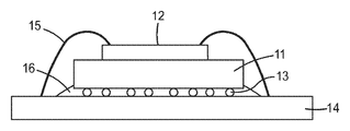
최근에는, 반도체 패키지에 3-차원 통합이 적용되었으며, 여기에서는 반도체 칩이 적층되고 수직 방향으로 배선이 실행된다. 다양한 3 차원 구조를 갖는 반도체 패키지 또한 등장했다. 예를 들어, 도 1에 나타낸 것과 같은 반도체 패키지에서는, 제1 전자 구성요소(11)가 솔더 범프(13)를 통해 기판(14)에 전기적으로 연결되고, 제1 전자 구성요소의 상부에 배치된 제2 전자 구성요소(12)가 본딩 와이어(15)에 의해 기판에 전기적으로 연결된다. 이러한 유형의 반도체 패키지에서는, 본딩 와이어(15)가 기판에 접촉되는 곳까지 언더필링제(16)의 에지가 연장될 경우에 연결 결함과 같은 문제가 발생할 수 있으므로, 언더필링제의 유동성을 조정함으로써 에지의 위치를 정확하게 제어해야 한다.In recent years, three-dimensional integration has been applied to a semiconductor package, in which semiconductor chips are stacked and wiring is performed in a vertical direction. Semiconductor packages with various three-dimensional structures have also appeared. For example, in a semiconductor package such as that shown in FIG. 1, a first
다른 해결책은, 도 2에 나타낸 바와 같이 오버몰딩제를 사용하여 기판을 전자 구성요소에 연결하는 것이다. 도 2의 실시 형태에서는, 솔더 범프(23)를 통해 기판(24) 상에 배치된 전자 구성요소(21)를 오버몰딩제(26)로 덮는다. 본딩 와이어와 같은, 기판 이외의 요소에 오버몰딩제(26)의 에지(261)가 유해 효과를 갖지 않도록 하기 위하여, 에지(261)의 위치를 제어해야 한다.Another solution is to connect the substrate to the electronic component using an overmolding agent as shown in Fig. In the embodiment of FIG. 2, the
또한, 최근에는 반도체 칩 제조 공정의 효율을 증가시키기 위하여, 반도체 칩으로 다이싱하기 전에 반도체 웨이퍼 상에 반도체 패키지 수지 조성물을 직접 코팅하였다. 미국 특허 출원 공개 제US 2006/0194064 A1호에는 웨이퍼를 개별적인 칩으로 다이싱하기 전에 반도체 웨이퍼 상에 직접 코팅하는 경화성 언더필 봉지재 조성물이 기재되어 있다. 이러한 언더필링제를 반도체 웨이퍼 상에 코팅하고, 최종 완전 경화 전에 대략 100℃ 내지 대략 150℃의 온도에서 B-스테이지 고형화(B-stage solidification)를 실행하여, 웨이퍼를 개별적인 칩으로 다이싱하기 위해 평탄하고 비점착성인 고체 코팅을 형성한다. 이어서, 웨이퍼를 개별적인 칩으로 다이싱하고, 언더필링제를 가진 B-스테이지 가공된 칩을 이러한 언더필링제가 기판에 인접하도록 하는 상태로 기판 상에 배치하고, B-스테이지 전환 온도보다 더 높은 제2 온도에서 최종 완전 경화를 실행한다.Recently, in order to increase the efficiency of a semiconductor chip manufacturing process, a semiconductor package resin composition is directly coated on a semiconductor wafer before dicing into a semiconductor chip. U.S. Patent Application Publication No. US 2006/0194064 A1 describes a curable underfill encapsulant composition that is coated directly onto a semiconductor wafer prior to dicing the wafer into individual chips. This underfilling agent is coated on a semiconductor wafer and B-stage solidification is performed at a temperature of about 100 ° C to about 150 ° C prior to final complete curing to flatten the wafer into individual chips To form a non-sticky solid coating. Subsequently, the wafer was diced into individual chips and a B-stage machined chip with an underfilling agent was placed on the substrate with the underfilling agent abutting the substrate and a second temperature higher than the B- The final full cure is performed.
본 발명의 반도체 패키지 수지 조성물의 유익한 제품 속성은, 기판 또는 전자 구성요소 상에 사용되는 경우에 낮은 점도를 달성하기 위한 모듈, 열팽창 계수, 및 유리 전이점(Tg)에 있어서의 적절한 범위; 적용 후에 조성물의 점도(유동성)를 조정하는 능력; 및 완전 경화 후에 기판과 전자 구성요소 사이의, 또는 전자 구성요소들 사이의 연결의 확실성을 보장하는 능력을 포함한다. 또한, 기판 또는 전자 구성요소의 표면 상에 배치된 반도체 패키지의 일부에 그의 유동성을 조정하기 위하여 B-스테이지 전환을 적용하고(즉, 가열하는 경우에 조성물이 용융되지 않고 연화되도록 충분한 경화를 실행함), 다른 부분에는 B-스테이지 전환을 적용하지 않는 경우, 다른 유익한 제품 속성은, 양자 모두의 부분에 가열에 의한 최종 경화를 적용하는 경우에도 양자 모두의 부분이 유사한 모듈, 열팽창 계수, 및 유리 전이점(Tg)을 갖는다는 점을 포함한다.Advantageous product properties of the semiconductor package resin composition of the present invention are the modulus, coefficient of thermal expansion, and appropriate range of glass transition point (Tg) for achieving low viscosity when used on a substrate or electronic component; The ability to adjust the viscosity (flowability) of the composition after application; And the ability to ensure certainty of the connection between the substrate and the electronic component, or between the electronic components, after full curing. In addition, B-stage switching is applied to adjust the fluidity of the substrate or a portion of the semiconductor package disposed on the surface of the electronic component (i. E., Sufficient curing is performed to soften the composition without melting when heated ) And the other part does not have a B-stage transition, the other beneficial product attributes are that both parts of both apply a similar module, thermal expansion coefficient, and glass transition (Tg). ≪ / RTI >
일 태양에서, 본 개시는 반도체 패키지 수지 조성물을 제공하며, 그의 유동성은 광을 이용한 조사를 통한 경화에 의해 조정될 수 있고, 가열에 의한 최종 경화를 실행함으로써 이는 기판과 전자 구성요소 사이의, 또는 전자 구성요소들 사이의 확실한 연결을 보장할 수 있다.In one aspect, the disclosure provides a semiconductor package resin composition, the flowability of which can be adjusted by curing through irradiation with light, and by performing a final cure by heating, Thereby ensuring a reliable connection between the components.
일 실시 형태에서, 본 개시는 에폭시 수지, 경화제, 무기 입자, 및 광중합성 작용기를 함유하는 실란으로 표면 처리된 나노-입자를 함유하는 반도체 패키지 수지 조성물을 포함한다.In one embodiment, the disclosure comprises a semiconductor package resin composition containing an epoxy resin, a curing agent, an inorganic particle, and a nano-particle surface treated with a silane containing a photopolymerizable functional group.
다른 실시 형태에서, 본 개시는 (1) 전자 구성요소 및 기판 중 하나 이상을 제공하는 단계, (2) 제1 반도체 패키지 수지 조성물을 전자 구성요소 및/또는 기판 상에 배치하는 단계(여기서, 반도체 패키지 수지 조성물은 에폭시 수지, 경화제, 무기 입자, 및 광가교성 기를 함유하는 실란으로 표면 처리된 나노-입자를 함유함), (3) B-스테이지 전환 중에 제1 반도체 패키지 수지 조성물의 적어도 일부를 광으로 조사하는 단계, 및 (4) 가열에 의해 제1 반도체 패키지 수지 조성물을 경화시키는 단계를 포함하는, 반도체 패키지의 제조 방법을 제공한다.In another embodiment, the disclosure provides a method comprising: (1) providing at least one of an electronic component and a substrate; (2) disposing a first semiconductor package resin composition on an electronic component and / (3) at least a portion of the first semiconductor package resin composition is exposed to light during the B-stage transition, and the second semiconductor package resin composition comprises at least a portion of the first semiconductor package resin composition during the B- , And (4) curing the first semiconductor package resin composition by heating.
<도 1>
도 1은, 선행 기술 반도체 패키지의 단면도이다.
<도 2>
도 2는, 오버몰딩제를 가진 선행 기술 반도체 패키지의 단면도이다.
<도 3>
도 3은, 본 발명의 실시 형태에 따른 반도체 패키지 제조 방법을 사용하여 제조한 반도체 패키지의 단면도이다.
<도 4a>
도 4a는, 반도체 패키지 수지 조성물이 전자 구성요소 상에 배치되는, 본 발명의 실시 형태에 따른 반도체 패키지 제조 방법의 단계의 개략적 단면도이다.
<도 4b>
도 4b는, 반도체 패키지 수지 조성물의 일부에 광을 이용한 조사를 적용하는, 본 발명의 실시 형태에 따른 반도체 패키지 제조 방법의 단계의 개략적 단면도이다.
<도 4c>
도 4c는, 전자 구성요소가 기판에 접촉 결합되는, 본 발명의 실시 형태에 따른 반도체 패키지 제조 방법의 단계의 개략적 단면도이다.
<도 5a>
도 5a는, 반도체 패키지 수지 조성물이 그 위에 인쇄된 지지체가 범프가 제공된 웨이퍼 상에 적층되는, 본 발명의 실시 형태에 따른 반도체 패키지 제조 방법의 단계의 개략도이다.
<도 5b>
도 5b는, 범프가 제공되고 그 위에 제1 반도체 패키지 수지 조성물이 배치된, 본 발명의 실시 형태에 따른 웨이퍼의 개략도이다.
<도 5c>
도 5c는, 반도체 패키지 수지 조성물의 B-스테이지 전환 후에 웨이퍼가 기판에 접촉 결합되는, 본 발명의 실시 형태에 따른 반도체 패키지 제조 방법의 단계의 개략도이다.
<도 6>
도 6은, 범프가 제공되지 않은 표면 상에 반도체 패키지 수지 조성물이 배치되는, 본 발명의 실시 형태에 따른 전자 구성요소의 도면이다.
<도 7a>
도 7a는, 반도체 패키지 수지 조성물에 광을 이용한 조사에 의한 B-스테이지 전환을 적용하는, 본 발명의 실시 형태에 따른 반도체 패키지 제조 방법의 단계의 개략적 단면도이다.
<도 7b>
도 7b는, 전자 구성요소가 기판에 접촉 결합되는, 본 발명의 실시 형태에 따른 반도체 패키지 제조 방법의 단계의 개략적 단면도이다.
<도 7c>
도 7c는, 본 발명의 실시 형태에 따른 반도체 패키지 제조 방법을 사용하여 제조한 반도체 패키지의 단면도이다.
<도 8a>
도 8a는, 제1 반도체 패키지 수지 조성물이 기판의 표면 상에 배치되는, 본 발명의 실시 형태에 따른 반도체 패키지 제조 방법의 단계의 개략적 단면도이다.
<도 8b>
도 8b는, 제2 반도체 패키지 수지 조성물이 기판의 표면 상에 배치되는, 본 발명의 실시 형태에 따른 반도체 패키지 제조 방법의 단계의 개략적 단면도이다.
<도 8c>
도 8c는, 본 발명의 실시 형태에 따른 반도체 패키지 제조 방법을 사용하여 제조한 반도체 패키지의 단면도이다.
<도 9>
도 9는, 본 발명의 실시 형태에 따른 반도체 패키지 제조 방법을 사용하여 제조한 반도체 패키지의 단면도이다.
<도 10>
도 10은, 본 발명의 실시 형태에 따른 반도체 패키지 수지 조성물의 유동성을 나타내는 그래프이다.
<도 11>
도 11은, 본 발명의 실시 형태에 따른 반도체 패키지 수지 조성물의 광경화성을 나타내는 그래프이다.
<도 12>
도 12는, 본 발명의 실시 형태에 따른 반도체 패키지 제조 방법을 사용하여 제조한 반도체 패키지의 단면을 나타내는 사진이다.
[발명의 상세한 설명]
본 명세서에서 모든 수는 용어 "약"에 의해 수식되는 것으로 간주된다. 종점에 의한 수치 범위의 언급은 그 범위 내에 포함되는 모든 수를 포함한다(예를 들어, 1 내지 5는 1, 1.5, 2, 2.75, 3, 3.80, 4, 및 5를 포함한다). 본 명세서에 언급된 모든 부는 달리 표시되지 않으면 중량 기준이다.
본 발명의 반도체 패키지 수지 조성물에 사용하기에 적합한 에폭시 수지는, 지방족, 지환족, 방향족, 또는 헤테로사이클릭 단량체성, 또는 올리고머성 에폭시 화합물을 포함하나 이로 제한되지 않는다. 일반적으로 이들 재료는, 평균적으로 분자당 하나 이상의 중합성 에폭시 기를 가지며, 분자당 1.5개 이상 또는 2개 이상의 중합성 에폭시 기를 가질 수 있다. 소정의 모드에서는, 분자당 3개 또는 4개의 중합성 에폭시 기를 갖는 다작용성 에폭시 화합물을 사용하는 것이 가능하다. 에폭시 화합물은 순수한 화합물일 수 있거나, 분자당 1개, 2개, 또는 그 이상의 에폭시 기를 함유하는 화합물의 혼합물일 수 있다.
상기 언급된 에폭시 화합물은 임의의 유형의 주쇄를 가질 수 있으며, 치환기를 함유할 수 있다. 적합한 치환기의 예는, 할로겐, 에스테르 기, 에테르, 설포네이트 기, 실록산 기, 니트로 기, 포스페이트 기 등을 포함하나 이로 제한되지 않는다. 에폭시 화합물의 에폭시 당량값은 일반적으로 50 내지 2000의 범위 내에서 변경될 수 있다.
올리고머성 에폭시 화합물의 예는, 말단 에폭시 기를 갖는 선형 올리고머(예를 들어, 폴리옥시알킬렌 글리콜의 다이글리시딜 에테르), 골격형 에폭시 단위를 갖는 올리고머(예를 들어, 폴리부타다이엔 폴리에폭사이드), 또는 펜던트 에폭시 기를 갖는 올리고머(예를 들어, 글리시딜 메타크릴레이트 올리고머 또는 코-올리고머)를 포함하나 이로 제한되지 않는다.
소정의 모드에서는, 하기의 화학식으로 나타내어지는 글리시딜 에테르 단량체를 사용하는 것이 가능하다.

상기 화학식에서, R은 n의 원자가를 갖는 라디칼이고, n은 1 내지 6의 정수이다. R은 방향족 기, 지환족 기, 지방족 기, 또는 그의 조합일 수 있다. 전형적인 에폭시 화합물은, 다가 페놀을 과량의 에피클로로하이드린과 같은 클로로하이드린과 반응시킴으로써 얻어진 다가 페놀의 글리시딜 에테르(예를 들어, 2,2-비스-(2,3-에폭시프로폭시페놀)-프로판)를 포함하나 이로 제한되지 않는다. 특히, 방향족 에폭시 화합물, 지환족 에폭시 화합물, 지방족 에폭시 화합물 등을 사용하는 것이 가능하다.
적합한 방향족 에폭시 화합물은, 비스페놀 A의 다이글리시딜 에테르(비스페놀 A 유형 에폭시 수지), 비스페놀 F의 다이글리시딜 에테르(비스페놀 F 유형 에폭시 수지), 4,4'-다이하이드록시바이페닐의 다이글리시딜 에테르, 이들 다이글리시딜 에테르의 올리고머, 크레졸 노볼락 수지의 폴리글리시딜 에테르(크레졸 노볼락 유형 에폭시 수지), 및 페놀 노볼락 수지의 폴리글리시딜 에테르(페놀 노볼락 유형 에폭시 수지)를 포함하나 이로 제한되지 않는다.
예시적인 지환족 에폭시 화합물은 상기 언급된 방향족 에폭시 화합물을 수소화함으로써 얻어진 화합물, 예를 들어, 수소화 비스페놀 A 유형 에폭시 화합물 및 수소화 비스페놀 F 유형 에폭시 화합물을 포함하나 이로 제한되지 않는다. 또한, 사이클로헥센 옥사이드 기를 함유하는 화합물, 예를 들어, 비닐 사이클로헥센 모노옥사이드, 1,2-에폭시-4-비닐 사이클로헥산, 1,2:8,9-다이에폭시리모넨, 3,4-에폭시사이클로헥센일메틸-3',4'-에폭시사이클로헥센 카르복실레이트, 및 에폭시 사이클로헥산 카르복실레이트, 예를 들어, 3,4-에폭시사이클로헥센일메틸-3,4-에폭시사이클로헥산 카르복실레이트, 3,4-에폭시-2-메틸사이클로헥실메틸-3,4-에폭시-2-메틸사이클로헥산 카르복실레이트, 및 비스(3,4-에폭시-6-메틸사이클로헥실메틸) 아디페이트를 사용하는 것이 가능하다.
적합한 지방족 에폭시 화합물은 지방족 다가 알코올의 글리시딜 에테르 또는 그의 알킬렌 옥사이드 부가물을 포함하나 이로 제한되지 않는다. 예를 들어, 에틸렌 글리콜 다이글리시딜 에테르, 다이(에틸렌 글리콜) 다이글리시딜 에테르, 프로필렌 글리콜 다이글리시딜 에테르, 트라이(프로필렌 글리콜) 다이글리시딜 에테르, 네오펜틸 글리콜 다이글리시딜 에테르, 1,4-부탄 다이올 다이글리시딜 에테르, 1,6-헥산 다이올 다이글리시딜 에테르, 트라이메틸올프로판 트라이글리시딜 에테르, 트라이메틸올프로판 다이글리시딜 에테르, 폴리(에틸렌 글리콜) 다이글리시딜 에테르 등을 그의 예로 들 수 있다.
상기 언급된 에폭시 수지에 부가하여, 할로겐화 에폭시 수지(예를 들어, 브롬화 비스페놀 유형 에폭시 수지) 또는 글리시딜아미노 기를 갖는 에폭시 화합물을 사용하는 것이 가능하다. 글리시딜아미노 기를 갖는 에폭시 화합물은 에피할로하이드린의 작용을 통해 아민을 에폭시화함으로써 얻어진 에폭시 화합물(에폭시 수지)이며, 그의 예는 아미노페놀 유형 에폭시 수지, 트라이글리시딜 아이소시아누레이트, 테트라글리시딜 다이아미노다이페닐메탄, 테트라글리시딜 메타-자일렌다이아민, 및 헥사글리시딜 트라이아미노벤젠을 포함한다.
아미노페놀 유형 에폭시 수지는 당업자에게 공지된 방법을 사용하여 아미노페놀을 에폭시화함으로써 얻어진다. 아미노페놀의 예는, 2-아미노페놀, 3-아미노페놀, 4-아미노페놀, 2-아미노-m-크레졸, 2-아미노-p-크레졸, 3-아미노-o-크레졸, 4-아미노-m-크레졸, 및 6-아미노-m-크레졸과 같은 아미노페놀 및 아미노크레졸을 포함하나 이로 제한되지 않는다.
사용하기에 적합한 다른 에폭시 수지는, 글리시돌의 아크릴산 에스테르(예를 들어, 글리시딜 아크릴레이트 및 글리시딜 메타크릴레이트)와 하나 이상의 공중합성 비닐 화합물과의 공중합체를 포함한다. 이러한 유형의 공중합체는 스티렌-글리시딜 메타크릴레이트 및 메틸 메타크릴레이트-글리시딜 아크릴레이트 공중합체를 포함한다. 또한, 에폭시-작용성 규소를 사용하는 것도 가능하며, 이는 규소 원자가 에폭시알킬 기로 치환된 폴리다이메틸 실록산이다.
상기 언급된 에폭시 수지 중에서, 비스페놀 A 유형 에폭시 수지, 비스페놀 F 유형 에폭시 수지, 또는 아미노페놀 유형 에폭시 수지를 사용하는 것이 반도체 패키지 수지 조성물의 최종 경화 후 특성의 관점에서 바람직하다. 또한, 반도체 패키지 수지 조성물의 점도와 최종 경화 후 특성 사이의 균형을 얻는 관점에서, 비스페놀 A 유형 에폭시 수지 및 비스페놀 F 유형 에폭시 수지 양자 모두 또는 비스페놀 A 유형 에폭시 수지 및 비스페놀 F 유형 에폭시 수지에 아미노페놀 유형 에폭시 수지를 추가로 첨가함으로써 얻어진 3-구성요소 시스템을 사용하는 것이 바람직하다. 구체적으로, 산물 ZX1059(니폰 스틸 케미칼 컴퍼니 리미티드(Nippon Steel Chemical Co., Ltd.)에 의해 제조된 비스페놀 A와 비스페놀 F의 혼합물) 또는 아미노페놀 유형 에폭시 jER(등록상표) 630(미쯔비시 케미칼 코포레이션(Mitsubishi Chemical Corporation)에 의해 제조)을 사용하는 것이 가능하며, 이들 양자 모두는 구매가능하다.
에폭시 수지의 블렌딩 양은 일반적으로 반도체 패키지 수지 조성물의 총량에 대해 50 질량% 이하, 일부 모드에서는 10 내지 40 질량%이다.
본 발명의 반도체 패키지 수지 조성물에 함유된 경화제는, 에폭시 화합물을 열경화시키기 위해 통상적으로 사용되는 경화제일 수 있다. 그의 구체적인 예는, 아미노 화합물, 산 무수물 화합물, 아미드 화합물, 페놀계 화합물, 트라이플루오르화 붕소 착물 화합물, 예를 들어, BF3-모노에탄올아민, 이미다졸, 예를 들어, 2-에틸-4-메틸이미다졸, 하이드라지드, 예를 들어, 아미노다이하이드라지드, 구아니딘, 예를 들어, 테트라메틸구아니딘, 및 다이시안다이아미드를 포함하나 이로 제한되지 않는다. 경화제는 단일 경화제 또는 상이한 경화제의 혼합물일 수 있다. 점도의 관점에서, 산 무수물 화합물이 바람직하다.
비-방향족 산 무수물 화합물을 사용하는 것이 적합하다. 예를 들어, 헥사하이드로프탈산 무수물, 3-메틸헥사하이드로프탈산 무수물, 4-메틸헥사하이드로프탈산 무수물, 1-메틸노르보르난-2,3-다이카르복실산 무수물, 5-메틸노르보르난-2,3-다이카르복실산 무수물, 노르보르난-2,3-다이카르복실산 무수물, 1-메틸나드산 무수물, 5-메틸나드산 무수물, 나드산 무수물, 테트라하이드로프탈산 무수물, 3-메틸테트라하이드로프탈산 무수물, 4-메틸테트라하이드로프탈산 무수물, 도데센일석신산 무수물 등을 사용하는 것이 적합하다.
이들 중에서, 화합물 내에 이중 결합을 갖지 않는 헥사하이드로프탈산 무수물, 3-메틸헥사하이드로프탈산 무수물, 4-메틸헥사하이드로프탈산 무수물, 1-메틸노르보르난-2,3-다이카르복실산 무수물, 5-메틸노르보르난-2,3-다이카르복실산 무수물, 또는 노르보르난-2,3-다이카르복실산 무수물이 특히 적합하다. 4-메틸헥사하이드로프탈산 무수물과 헥사하이드로프탈산 무수물의 혼합물(예를 들어, 뉴 재팬 케미칼 컴퍼니 리미티드(New Japan Chemical Co., Ltd.)에 의해 제조된 릭애시드(Rikacid) MH-700(4-메틸헥사하이드로프탈산 무수물/헥사하이드로프탈산 무수물 비 = 70/30))이 특히 적합하며, 이는 이 혼합물을 함유하는 반도체 패키지 수지 조성물이 낮은 점도를 가지며 거의 결정화되지 않기 때문이다.
예시적인 페놀계 경화제는, 비스페놀 A, 비스페놀 F, 비스페놀 S, 4,4'-바이페닐페놀, 테트라메틸 비스페놀 A, 다이메틸 비스페놀 A, 테트라메틸 비스페놀 F, 다이메틸 비스페놀 F, 테트라메틸 비스페놀 S, 다이메틸 비스페놀 S, 테트라메틸-4,4'-바이페놀, 다이메틸-4,4'-바이페닐페놀, 1-(4-하이드록시페닐)-2-[4-페닐]프로판, 2,2'-메틸렌-비스(4-메틸-6-tert-부틸페놀), 4,4'-부틸리덴-비스(3-메틸-6-tert-부틸페놀), 트리스하이드록시페닐메탄, 레소르시놀, 하이드로퀴논, 피로갈롤, 다이아이소프로필리덴, 테르펜 골격을 갖는 페놀, 플루오렌 골격을 갖는 페놀, 예를 들어,1,1-다이-4-하이드록시페닐플루오렌, 페놀화 폴리부타다이엔, 페놀, 크레졸, 에틸페놀, 부틸페놀, 옥틸페놀, 및 노볼락 수지, 예를 들어, 비스페놀 A, 비스페놀 F, 비스페놀 S, 나프톨, 테르펜 다이페놀 등과 같은 페놀을 원재료로 사용하여 얻어진 노볼락 수지, 자일릴렌 골격을 갖는 페놀 노볼락 수지, 다이사이클로펜타다이엔 골격을 갖는 페놀 노볼락 수지, 바이페닐 골격을 갖는 페놀 노볼락 수지, 플루오렌 골격을 갖는 페놀 노볼락 수지, 및 퓨란 골격을 갖는 페놀 노볼락 수지를 포함하나 이로 제한되지 않는다.
예시적인 아미노계 경화제는, 지방족 아민, 예를 들어, 다이에틸렌트라이아민, 트라이에틸렌테트라민, 또는 테트라에틸렌펜타민, 방향족 아민, 예를 들어, 다이아미노다이페닐메탄, 다이아미노다이페닐설폰, 메타-자일렌다이아민, 및 방향족 아민과 알데히드의 축합 산물, 폴리아미도아민을 포함하나 이로 제한되지 않는다.
얻어지는 경화 산물의 특성의 관점에서, 경화제의 블렌딩 양은 에폭시 수지의 블렌딩 양과 대략 동일하다. 일반적으로, 경화제의 블렌딩 양은 반도체 패키지 수지 조성물의 총 중량에 대해 5 내지 15 질량%이다.
무기 입자는 본 발명의 반도체 패키지 수지 조성물 내에 실질적으로 균질하게 분산된다. 반도체 패키지 수지 조성물에 높은 탄성률 및 낮은 열팽창 계수를 부여하기 위하여 무기 입자를 사용하며, 단일 유형 또는 2가지 이상의 유형의 무기 입자의 조합을 사용하는 것이 가능하다. 일반적으로, 이들 무기 입자는 실리카(용융 실리카, 결정질 실리카), 알루미나, 규산칼슘, 탄산칼슘, 티탄산칼륨, 탄화규소, 질화규소, 질화알루미늄, 질화붕소, 베릴리아, 지르코니아, 지르콘, 포스테라이트, 스테아타이트, 스피넬, 멀라이트, 또는 티타니아와 같은 분말, 또는 이들 분말을 구형화함으로써 얻어진 비드, 유리 섬유 등일 수 있다. 단일 유형 또는 2가지 이상의 유형의 조합의 이들 무기 입자를 사용하는 것이 가능하다.
상기 언급된 무기 입자 중에서, 열팽창 특성의 관점에서는 용융 실리카가 특히 적합하고, 높은 열 전도성을 갖는 관점에서는 결정질 실리카 및 알루미나가 특히 적합하다. 또한, 유기 졸로부터 실리카 입자를 무기 입자로서 제조하는 경우, 그의 입자 크기 분포가 좁으므로, 수지 조성물 내에 입자를 효과적으로 분포시키는 것이 가능하다. 또한, 무기 입자의 1차 입자의 형상이 특히 중요하지는 않으나, 미세한 갭 내로 유동하고 침투하는 것이 가능해지는 관점에서 구형 입자가 바람직하다.
또한, 반도체 패키지 수지 조성물의 유동성의 관점에서, 무기 입자는 작은 평균 입자 직경 및 좁은 입자 크기 분포를 갖는다. 반도체 패키지 수지 조성물을 좁은 갭 내로 밀어넣을 때 무기 입자가 적체되기 쉬우므로, 본 발명에 사용되는 무기 입자의 평균 입자 직경은 10 ㎛ 이하이다. 일 실시 형태에서, 무기 입자의 평균 입자 직경은 특히 5 ㎛ 이하, 더욱 특히 3 ㎛ 이하, 더욱 더 특히 2 ㎛ 이하이다. 그러나, 무기 입자의 평균 입자 직경의 하한은 특히 한정되지 않으나, 유동성의 관점에서, 평균 입자 직경은 실리카 입자의 경우에 0.05 ㎛ 이상이고 알루미나 입자의 경우에 0.1 ㎛ 이상이다. 일 실시 형태에서, 반도체 패키지 수지 조성물 내의 무기 입자의 입자 직경은 "평균 입자 직경 ± (평균 입자 직경 × 0.3)"(예를 들어, 1 ± 0.3 ㎛)의 범위 내에 있다. 무기 입자의 평균 입자 직경 및 입자 크기 분포는 전자 현미경 또는 레이저 산란 장치로 측정할 수 있다. 또한, 수지 조성물 내의 입자의 분산성을 훼손하지 않는 정도까지 무기 입자를 표면 처리할 수 있다.
졸-겔 방법에 의해 제조되고 입자 크기 분포가 좁은 실리카 입자가 무기 입자로서 특히 적합하고, 평균 입자 직경이 0.8 내지 1.8 ㎛인, 졸-겔 방법에 의해 제조되고 입자 크기 분포(평균 입자 직경 ± (평균 입자 직경 × 0.3))가 좁은 용융 실리카가 더욱 더 적합하다. 이러한 무기 입자는, 예를 들어, 실리카 KE-S150 및 KE-S10(니폰 쇼쿠바이 컴퍼니 리미티드(Nippon Shokubai Co., Ltd.)에 의해 졸-겔 방법을 사용하여 제조), 실리카 HPS-1000(토아고세이 컴퍼니 리미티드(Toagosei Co., Ltd.)에 의해 졸-겔 방법을 사용하여 제조), 또는 실리카 SS-07, SS-10, 및 SS-14(토쿠야마 코포레이션(Tokuyama Corporation)에 의해 졸-겔 방법에 의해 제조)로서 구매가능하다.
본 발명의 반도체 패키지 수지 조성물은 광중합성 작용기를 함유하는 실란으로 표면 처리된 나노-입자를 함유한다. 광(예를 들어, 자외선 방사 및/또는 가시광)에 노출시킴으로써, 짧은 기간(수 초 내지 수십 초) 동안의 조사 및 B-스테이지 전환의 실행(즉, 가열하는 경우에 조성물이 용융되지 않고 연화되도록 충분한 경화를 실행함)에 의해 수지 조성물의 유동성을 조정하는 것이 가능하다.
일반적으로, 이들 나노-입자는 실리카(예를 들어, 용융 실리카 또는 결정질 실리카), 알루미나, 규산칼슘, 탄산칼슘, 티탄산칼륨, 탄화규소, 질화규소, 질화알루미늄, 질화붕소, 베릴리아, 지르코니아, 지르콘, 포스테라이트, 스테아타이트, 스피넬, 멀라이트, 또는 티타니아와 같은 분말, 또는 이들 분말을 구형화함으로써 얻어진 비드, 유리 섬유 등일 수 있다. 단일 유형 또는 2가지 이상의 유형의 조합의 이들 무기 입자를 사용하는 것이 가능하다.
나노-입자 중에서, 화학적 안정성의 관점에서는 실리카 입자가 특히 적합하고, 열 전도성의 관점에서는 알루미나가 바람직하다. 또한, 유기 졸로부터 실리카 입자를 나노-입자로서 제조하는 경우, 그의 입자 크기 분포가 좁으므로, 수지 조성물 내에 입자를 효과적으로 분포시키는 것이 가능하다. 또한, 나노-입자의 형상이 특히 중요하지는 않으나, 미세한 갭 내로 유동하고 침투하는 것이 가능해지는 관점에서 구형 입자가 특히 적합하다.
본 발명의 조성물에 사용하기에 적합한 나노-입자의 평균 입자 직경은 1 ㎚ 내지 1 ㎛ 미만의 범위이다. 광중합성 작용기의 반응성을 개선하기 위하여, 바람직하게는, 나노-입자의 평균 입자 직경은 작다. 일반적으로, 나노-입자의 평균 입자 직경은 5 ㎚ 내지 500 ㎚, 특히 10 ㎚ 내지 300 ㎚, 더욱 특히 10 ㎚ 내지 100 ㎚일 수 있다.
광에 의해 중합될 수 있는 작용기는 CH2=CH-C(=O)-O- 기, CH2=CCH3-C(=O)-O- 기, 글리시딜 기, 비닐 기 등을 포함한다.
광중합성 작용기를 함유하는 실란은 3-(트라이메톡시실릴)프로필 메타크릴레이트, 비닐트라이메톡시실란, 비닐트라이에톡시실란, p-스티릴트라이메톡시실란, 또는 (메트)아크릴레이트 실란, 예를 들어, 3-메타크릴옥시프로필 트라이메톡시실란, 3-메타크릴옥시프로필 트라이메톡시실란, 메틸다이메톡시실란, 또는 3-아크릴옥시프로필 트라이메톡시실란일 수 있다. 이들은 화학적 결합(공유 결합 또는 이온 결합)에 의하거나 강한 물리적 결합에 의해 나노-입자의 표면에 결합될 수 있다.
방법
광중합성 작용기를 함유하는 실란으로 표면 처리된 나노-입자는, 예를 들어, 하기의 방법을 사용하여 제조할 수 있다.
광중합성 작용기를 함유하는 실란을 용매에 첨가함으로써 액체를 제조한 후, 이 액체를 콜로이드성 실리카에 교반 하에 첨가한다. 교반 후에, 10 내지 20 시간 동안 승온에서 가열함으로써 표면-개질된 나노-입자를 함유하는 반응 혼합물을 얻는다.
이어서, 반응 혼합물을 주위 온도로 냉각시키고, 회전식 증발기에 의해 혼합물로부터 물을 제거한다. 그 다음에, 용매를 첨가하고 임의의 잔류하는 물을 증발기에 의해 제거한다(이 단계는 수회 반복될 수 있음). 이어서, 반응 혼합물에 용매를 첨가하여 그 안의 고체 함량을 조정한다. 이어서, 1.0 ㎛ 유리 미세섬유 필터를 통해 반응 혼합물 분산액을 여과하여 침강물을 제거하고 광중합성 작용기를 함유하는 실란으로 표면 처리된 나노-입자를 용매 중에 함유하는 분산액을 얻는다.
반도체 패키지 수지 조성물 내의 무기 입자 및 광중합성 작용기를 함유하는 실란으로 표면 처리된 나노-입자의 양은, 얻어진 경화된 물체의 열팽창 계수의 관점에서는 반도체 패키지 수지 조성물의 전체량에 대해 60 질량% 이상이고, 수지 조성물의 점도의 관점에서는 반도체 패키지 수지 조성물의 전체량에 대해 90 질량% 이하이다. 무기 입자의 블렌딩 양이 이 범위 내에 들어오는 경우, 열팽창 계수가 35 ppm 이하인 경화 산물을 얻는 것이 일반적으로 가능하며, 본 발명의 반도체 패키지 수지 조성물을 반도체 패키지 수지 조성물로서 사용하는 것 또한 가능하다.
광중합성 작용기를 함유하는 실란으로 표면 처리된 나노-입자의 양은 나노-입자 및 무기 입자의 총량에 대해 0.1 질량% 이상이고 10 질량% 이하이다. B-스테이지 전환을 실행하는 경우에, 첨가되는 나노-입자의 양은 수지 조성물의 목적하는 점도(유동성)를 얻기 위해 조정한다. 광중합성 작용기를 함유하는 실란으로 표면 처리된 나노-입자의 양이 너무 적다면, 광으로 조사하는 경우에도 수지 조성물의 점도(유동성)를 조정하는 것이 불가능하고, 이 양이 너무 많다면, 완전한 경화가 일어나고, 광으로 조사한 후의 열 경화 중에 경화시의 수축이 일어나며, 경화 산물에 균열이 나타난다.
본 발명의 반도체 패키지 수지 조성물에 광중합 개시제를 첨가하는 것이 특히 적합하다. 광중합 개시제의 예는, 벤조인, 벤조인 메틸 에테르, 벤조인 에틸 에테르, 벤조인 n-프로필 에테르, 벤조인 n-부틸 에테르, 벤질(benzil), 벤조페논, p-메틸벤조페논, 다이아세틸, 에오신, 티오닌, 미힐러 케톤(Michler's ketone), 아세토페논, 2-클로로티오잔톤, 안트라퀴논, 클로로안트라퀴논, 2-메틸안트라퀴논, α-하이드록시아이소부틸페논, p-아이소프로필-α-하이드록시아이소부틸페논, α,α'-다이클로로-4-페녹시아세토페논, 1-하이드록시-1-사이클로헥실아세토페논, 2,2-다이메톡시-2-페닐아세토페논, 메틸벤조인 포르메이트, 2-메틸-1-[4-(메틸티오)페닐]-2-모폴리노프로펜, 다이클로로티오잔톤, 다이아이소프로필티오잔톤, 페닐다이설파이드-2-니트로소플루오렌, 부티로인, 아니소아이소에틸 에테르, 아조비스아이소부티로니트릴, 테트라메틸티우람 다이설파이드 등을 포함하나 이로 제한되지 않는다. 그의 하나 이상의 유형을 사용할 수 있다.
유기 티타늄 화합물을 반도체 패키지 수지 조성물에 첨가할 수 있다. 유기 티타늄 화합물은 화합물 내에 가수분해성 기 또는 소수성 기를 가질 수 있다. 이러한 유기 티타늄 화합물은 일반적으로 티타늄 커플링제로서 공지되어 있다. 유기 티타늄 화합물은 무기 입자의 표면 상의 -OH 기와 반응하며, 예를 들어, 가수분해에 의해 알코올을 제거함으로써 티타늄과 공유 결합을 형성한다. 이론에 구애됨이 없이, 이는 무기 입자의 표면을 유기화하여 에폭시 수지 내의 무기 입자의 양호한 분산성을 유발하는 것으로 생각된다.
유기 화합물 내의 가수분해성 기는, 예를 들어, R1O-, -O-CH2-CH2-O-, 또는 -O-CH2-C(=O)-O- 등일 수 있다. 여기서, R1은 치환되거나 비치환된, 직쇄 또는 분지쇄 알킬 기, 알켄일 기, 아릴 기, 또는 아랄킬 기일 수 있다. 무기 입자와의 반응 후에 R1이 제거되므로(예를 들어, 알코올을 형성함으로써 제거됨), 제거 후에 R1은 다소 더 낮은 비등점을 갖는 기가 되는 것이 바람직하다. 그러므로, 특히 적합한 R1은 몇 개의 탄소 원자를 갖는 기, 특히 1 내지 10개의 탄소 원자(더욱 특히 1 내지 8개의 탄소 원자)를 갖는 치환되거나 비치환된, 직쇄 또는 분지쇄 알킬 기이다.
또한, 유기 티타늄 화합물 내의 소수성 기는 -O-C(=O)-R2, -O-S(=O)2-Ph-R2, -O-P(=O)(-OH)-O-P(=O)-(OR2)2, -O-P(=O)-(OR2)2, HO-P-(OR2)2, -O-(CH2)m-NH-(CH2)n-NH2 등일 수 있다. 여기서, Ph는 페닐 기를 나타내고, m 및 n은 각각 1 내지 10의 정수이며, R2는 치환되거나 비치환된, 직쇄 또는 분지쇄 알킬 기, 알켄일 기, 아릴 기, 또는 아랄킬 기일 수 있다. 무기 입자의 표면을 덮는 효율을 개선하기 위하여, R2는 특히 다수의 탄소 원자를 갖는 기, 더욱 특히 8 내지 30개의 탄소 원자를 갖는 치환되거나 비치환된, 직쇄 또는 분지쇄 알킬 기이다.
이들 중에서, -O-C(=O)-R2, HO-P-(OR2)2, 및 -O-(CH2)m-NH-(CH2)n-NH2가 반도체 패키지 수지 조성물 내의 무기 입자와의 반응성 및 반도체 패키지 수지 조성물의 감소된 점도의 관점에서 특히 적합한 소수성 기이다. 유동성의 관점에서는 -O-C(=O)-R2 또는 HO-P-(OR2)2가 더 적합하고, 티타늄 커플링제의 안정성의 관점에서는 -O-C(=O)-R2가 더 적합하다. 여기서, R2는 8 내지 30개의 탄소 원자, 바람직하게는 10 내지 30개의 탄소 원자를 갖는 치환되거나 비치환된, 직쇄 또는 분지쇄 알킬 기이다.
구체적으로, 티타늄 커플링제는, 예를 들어, 테트라알콕시 티타늄(예를 들어, 테트라에톡시 티타늄, 테트라아이소프로폭시 티타늄, 또는 테트라부톡시 티타늄), 테트라(에틸렌 글리콜) 티타네이트, 다이-n-부틸비스(트라이에탄올아민) 티타네이트, 다이-아이소프로폭시 비스(아세틸 아세토네이트)티타늄, 아이소프로폭시 티타늄 옥타노에이트, 아이소프로필 티타늄 트라이메타크릴레이트, 아이소프로필 티타늄 트라이아크릴레이트, 아이소프로필 트라이아이소스테아로일 티타네이트, 아이소프로필 트라이데실벤젠설포닐 티타네이트, 아이소프로필 트라이(부틸, 메틸피로포스페이트) 티타네이트, 테트라아이소프로필 다이(다이라우릴 포스파이트) 티타네이트, 다이메타크릴옥시아세테이트 티타네이트, 다이아크릴옥시아세테이트 티타네이트, 다이(다이옥틸 포스파이트)에틸렌 티타네이트, 아이소프로폭시 티타늄 트라이(다이옥틸 포스페이트), 아이소프로필 트리스(다이옥틸 피로포스페이트) 티타네이트, 테트라아이소프로필 비스(다이옥틸 포스파이트) 티타네이트, 테트라옥틸 비스(다이-트라이데실 포스파이트) 티타네이트, 테트라(2,2-다이알릴옥시메틸-1-부틸) 비스(다이-트라이데실)포스파이트 티타네이트, 비스(다이옥틸 피로포스페이트)옥시아세테이트 티타네이트, 트리스(다이옥틸 피로포스페이트)에틸렌 티타네이트, 아이소프로필 트라이-n-도데실벤젠설포닐 티타네이트, 아이소프로필 트라이옥타노일 티타네이트, 아이소프로필 다이메타크릴로일 아이소스테아로일 티타네이트, 아이소프로필 아이소스테아로일 다이아크릴릭 티타네이트, 아이소프로필 트라이(다이옥틸 포스페이트) 티타네이트, 아이소프로필 트라이큐밀페닐 티타네이트, 아이소프로필 트라이(N-아미노에틸-아미노에틸) 티타네이트 등일 수 있다.
아지노모토 파인-테크노 컴퍼니 인코포레이티드(Ajinomoto Fine-Techno Co., Inc.)에 의해 판매되는 플레낙트(Plenact)(등록상표) 시리즈의 KRTTS(아이소프로필트라이아이소스테아로일 티타네이트(CH3)2CHOTi[OCO(CH2)14CH(CH3)2]3), KR 46B(테트라옥틸비스(다이-트라이데실포스파이트) 티타네이트), KR 55(테트라(2,2-다이알릴옥시메틸-1-부틸) 비스(다이-트라이데실) 포스파이트 티타네이트), KR 41B(테트라아이소프로필비스(다이옥틸포스파이트) 티타네이트), KR 38S(아이소프로필트리스(다이옥틸피로포스페이트) 티타네이트), KR 138S(비스(다이옥틸피로포스페이트)옥시아세테이트 티타네이트), KR 238S(트리스(다이옥틸피로포스페이트)에틸렌 티타네이트), 338X(아이소프로필다이옥틸피로포스페이트 티타네이트), KR 44(아이소프로필트라이(N-아미노에틸아미노에틸) 티타네이트), KR 9SA(아이소프로필트리스(도데실벤질페닐) 티타네이트) 등을 사용할 수 있다. 플레낙트 KR TTS, KR 46B, 및 KR 9SA 가 적합하고, 플레낙트 KR TTS 및 KR 46B가 더욱 적합하다.
반도체 패키지 수지 조성물의 점도를 감소시키는 관점에서, 유기 티타늄 화합물의 블렌딩 양은 반도체 패키지 수지 조성물의 총량에 대해 1 질량% 이상, 특히 2 질량% 이상, 더욱 특히 2.5 질량% 이상이다. 그러나, 얻어지는 경화 산물의 감소된 유리 전이 온도 및 탄성률의 관점에서, 유기 티타늄 화합물의 블렌딩 양은 반도체 패키지 수지 조성물의 총량에 대해 5 질량% 이하, 특히 4 질량% 이하, 더욱 특히 3 질량% 이하이다.
유기 인산 화합물 중에서, 본 발명의 반도체 패키지 수지 조성물에 사용될 수 있는 인산 에스테르는 인산과 알코올에 탈수축합(dehydrocondensation)을 적용함으로써 얻어지는 에스테르를 포함하나 이로 제한되지 않는다. 상기 언급된 유기 티타늄 화합물에 인산 에스테르를 추가로 첨가함으로써 인산 에스테르는 티타늄과 약한 결합, 예를 들어, 배위 결합을 형성한다. 결과적으로, 유기 티타늄 화합물에 의해 유기화되는 무기 입자의 표면 상의 유기층의 깊이가 증가한다.
구체적으로 인산 에스테르는, 인산(O-P(OH)3) 내의 3개의 수소 원자 중 일부 또는 전부가 유기 기에 의해 대체된 구조를 갖는다. 1개, 2개, 및 3개의 수소 원자가 대체된 화합물은 각각 인산 모노에스테르(P(OZ)3), 인산 다이에스테르(HOP(OZ)2), 및 인산 트라이에스테르((HO)2POZ)로서 공지되어 있다. 여기서, Z는 10 내지 50개의 탄소 원자를 갖는 치환되거나 비치환된 알킬 기, 페닐 기, 폴리에스테르, 또는 폴리카프로락톤 등을 나타낸다. 무기 입자의 표면 상에 형성되는 유기층의 두께를 증가시키는 관점에서, Z는 특히 높은 분자량을 갖는다. 특히 200 내지 20,000의 중량 평균 분자량, 및 더욱 특히 300 내지 10,000의 중량 평균 분자량.
예를 들어, 다이메틸 포스페이트, 다이에틸 포스페이트, 다이프로필 포스페이트, 모노부틸 포스페이트, 다이부틸 포스페이트, 모노-2-에틸헥실 포스페이트, 다이-2-에틸헥실 포스페이트, 모노페닐 포스페이트, 모노-2-에틸헥실 포스파이트, 다이옥틸 포스페이트, 다이페닐 포스페이트 등을 상기 언급된 화합물로서 사용할 수 있다. 적합한 구매가능한 산물은 일본 소재의 BYK 케미칼스(BYK Chemicals)에 의해 제조되는 디스퍼빅(Disperbyk) 111을 포함하나 이로 제한되지 않는다.
상기 언급된 인산 에스테르 중에서, 무기 입자의 분산의 관점에서 인산 다이에스테르가 특히 적합하며, Z가 폴리카프로락톤인 인산 다이에스테르가 더욱 특히 적합하다.
반도체 패키지 수지 조성물의 점도를 감소시키는 관점에서, 인산 에스테르의 블렌딩 양은 반도체 패키지 수지 조성물의 총량에 대해 0.5 질량% 이상, 특히 1 질량% 이상, 더욱 특히 1.2 질량% 이상이다. 그러나, 얻어지는 경화 산물의 전기적 특성(절연 특성)의 감소를 야기할 가능성의 관점에서는, 인산 에스테르의 블렌딩 양은 반도체 패키지 수지 조성물의 총량에 대해 3 질량% 이하, 특히 2 질량% 이하, 더욱 특히 1.8 질량% 이하이다.
상기 언급된 바와 같이, 유기 티타늄 화합물을 인산 에스테르와 조합함으로써, 에폭시 수지 내의 무기 입자의 분산성을 개선하고 얻어지는 반도체 패키지 수지 조성물의 유동성을 개선하는 것이 가능하다. 특히, R3OTi(OCOR4H)3 또는 (R3O)4Ti[HOP(OR4)2](여기서, R3은 3 내지 8개의 탄소 원자를 갖는 직쇄 또는 분지쇄 알킬 기를 나타내고 R4는 10 내지 20개의 탄소 원자를 갖는 직쇄 또는 분지쇄 알킬 기를 나타냄)에 의해 나타내어지는 화학 구조를 갖는 유기 티타늄 화합물과 200 내지 20,000의 중량 평균 분자량을 가지며 HOP(OZ)2(여기서, Z는 10 내지 50개의 탄소 원자를 갖는 치환되거나 비치환된 알킬 기, 페닐 기, 폴리에스테르, 또는 폴리카프로락톤을 나타냄)에 의해 나타내어지는 화학 구조를 갖는 인산 다이에스테르의 조합이 특히 적합하다.
상기 언급된 구성요소에 부가하여, 본 발명의 반도체 패키지 수지 조성물은 반응 촉진제(reaction accelerator) 또한 함유할 수 있다. 여기서, 에폭시 수지와 경화제 사이의 반응을 촉진하기 위해 사용되는 반응 촉진제는 당업자에게 공지된 반응 촉진제, 예를 들어, 사이클로아미딘 화합물, 3차 아민, 4차 암모늄 염, 이미다졸, 루이스산으로서 작용하는 유기 금속 화합물, 인계 화합물, 예를 들어, 유기 포스핀, 예를 들어, 트라이페닐 포스핀, 또는 그의 유도체 또는 테트라페닐 붕소 염일 수 있다. 단일 반응 촉진제 또는 그의 2가지 이상의 유형의 조합을 사용할 수 있다. 또한, 반응 촉진 효과가 달성되는 한, 반응 촉진제의 블렌딩 양은 특히 제한되지 않는다.
또한, 반도체 소자의 내습성 및 고온 노출 특성을 개선하기 위하여, 본 발명의 반도체 패키지 수지 조성물 내에 이온 포획제를 블렌딩하는 것이 가능하다. 이온 포획제는 특히 제한되지 않으며, 당업자에게 공지된 임의의 이온 포획제를 사용하는 것이 가능하다. 특히, 하이드로탈사이트 또는 마그네슘, 알루미늄, 티타늄, 지르코늄, 또는 비스무스와 같은 원소의 함수 옥사이드를 사용하는 것이 가능하다.
추가로, 응력 완화제(stress relaxing agent), 예를 들어, 실리콘 고무 분말, 염료, 착색제, 예를 들어, 카본 블랙, 평활제, 소포제, 및 다른 무기 충전제(예를 들어, 난연 효과를 갖는 무기 충전제, 예를 들어, 수산화알루미늄, 수산화마그네슘, 규산아연, 또는 몰리브덴산아연) 등을 본 발명의 목적을 훼손하지 않는 수준으로 본 발명의 반도체 패키지 수지 조성물 내에 블렌딩할 수 있다. 또한, 적린, 인산 에스테르, 멜라민, 멜라민 유도체, 트라이아진 고리를 갖는 화합물, 질소-함유 화합물, 예를 들어, 시아누르산 유도체 또는 아이소시아누르산 유도체, 인- 및 질소-함유 화합물, 예를 들어, 사이클로포스파젠, 금속 화합물, 예를 들어, 산화아연, 산화철, 산화몰리브덴, 및 페로센, 산화안티몬, 예를 들어, 삼산화안티몬, 사산화안티몬, 및 오산화안티몬, 및 난연제, 예를 들어, 브롬화 에폭시 수지 등 또한 본 발명의 반도체 패키지 수지 조성물 내에 블렌딩할 수 있다.
상기 언급된 구성요소를 균일하게 분산시키고 블렌딩할 수 있는 한, 임의의 유형의 제조 방법을 사용하여 본 발명의 반도체 패키지 수지 조성물을 제조할 수 있다. 통상적인 제조 방법은, 특정 블렌딩 양의 원재료를 함께 블렌딩하거나 별도로 블렌딩하고, 교반하고, 용해시키고, 혼합 롤러, 압출기, 행성형 혼합기(planetary mixer) 등에서 필요한 경우에는 가열 및 냉각 중에 이들 구성요소를 블렌딩 및 분산시킨 후에, 냉각시키고 필요한 경우에는 거품을 제거하고 파쇄하는 것이다. 또한, 무기 입자를 제외한 모든 구성요소의 혼합물을 먼저 제조한 후, 이 혼합물에 무기 입자를 첨가하여 반도체 패키지 수지 조성물을 얻는 것 또한 가능하다. 또한, 요구되는 경우에는 반도체 패키지 수지 조성물을 성형 조건에 적절한 치수 및 중량을 갖는 태블릿으로 형성하는 것 또한 가능하다.
B-스테이지 전환이 이루어지도록 본 발명의 반도체 패키지 수지 조성물을 광중합에 의해 충분히 경화시킬 수 있다(즉, 가열하는 경우에 조성물이 용융되지 않고 연화되도록 충분한 경화를 실행함).
일 실시 형태에서, 본 발명의 반도체 패키지 수지 조성물의 최종 경화 산물은 10 내지 35 ppm의 열팽창 계수를 갖는다. 규소는 낮은 열팽창 계수를 가지므로, 반도체를 밀봉하는 경우에 규소를 밀봉하기 위해 사용되는 재료 또한 낮은 열팽창 계수를 갖는 것이 바람직하다. 열팽창 계수가 35 ppm을 초과한다면, 열 응력으로 인해 균열이 발생할 우려가 있다. 또한, TMA(열기계 분석기(Thermal Mechanical Analyzer))를 사용하여 열팽창 계수를 측정하는 것이 가능하다. 구체적으로, 리가쿠 코포레이션(Rigaku Corporation)에 의해 제조된 TMA 8310 열역학적 분석 기구로 열팽창 계수를 측정하는 것이 가능하다. 샘플(크기: 4 × 5 × 10 ㎣)을 질소 스트림 내에서 20℃/분의 속도로 가열하고, 10 mN의 하중을 적용하고, 압축 모드로 측정을 실행한다.
일 실시 형태에서, 본 발명의 반도체 패키지 수지 조성물의 최종 경화 산물은 60 내지 120℃의 유리 전이 온도(Tg) 및 5 내지 40 GPa의 탄성률(동적 저장 탄성률; E')을 갖는다. 유리 전이 온도 및 탄성률은 DMA(동적 기계 분석(dynamic mechanical analysis)) 기구를 사용하여 측정할 수 있다. 본 측정 방법은 레오메트릭 사이언티픽(Rheometric Scientific)에 의해 제조된 3점 곡선 모드의 고체 분석기(RSA-III)(변형률: 0.05%, 주파수: 1 Hz) 및 3℃/분의 속도로 가열되는 샘플(크기: 2 × 10 × 35 ㎣)을 사용하는 것을 포함한다.
구체적으로, 상기 언급된 장방형 샘플(크기: 2 × 10 × 35 ㎣)을 2개의 나이프 에지(25 ㎜ 분리됨) 상에 위치시키고 샘플의 중앙부를 내리눌러 샘플을 변형시키기 위한 하중 사용을 측정함으로써, 3점 곡선 방법을 사용하여 탄성률(동적 저장 탄성률)을 측정하는 것이 가능하다. 이 경우에, 변형률은 0.05%의 최대값을 갖는 사인파로서 적용되며, 하중 또한 사인파로서 측정된다(사인파 주파수는 1 Hz임).
반도체 패키지의 제조 방법
일 실시 형태에서, 본 발명은 (1) 전자 구성요소 및/또는 기판을 제공하는 단계, (2) 에폭시 수지, 경화제, 무기 입자, 및 광가교성 기를 함유하는 실란으로 표면 처리된 나노-입자를 함유하는 제1 반도체 패키지 수지 조성물을 전자 구성요소 및/또는 기판 상에 배치하는 단계, (3) 제1 반도체 패키지 수지 조성물의 일부 또는 전부를 광으로 조사하는 B-스테이지 전환 단계, 및 (4) 가열에 의해 제1 반도체 패키지 수지 조성물을 경화시키는 단계를 포함하는, 반도체 패키지의 제조 방법을 제공한다. 본 발명의 반도체 패키지 제조 방법을 사용하여 전자 구성요소를 다른 전자 구성요소에 연결하거나 전자 구성요소를 기판에 연결할 수 있다.
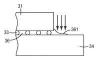
본 발명의 일 실시 형태에서는, 도 3에 나타낸 바와 같이, 전자 구성요소(31)와 기판(34)이 연결된 반도체 패키지가 제조된다. 전자 구성요소(31) 및 기판(34)을 제조한 후에, 제1 반도체 패키지 수지 조성물(36)을 전자 구성요소(31) 및/또는 기판(34)의 표면 상에 배치한다. 수지 조성물을 배치하는 방법은 저압 이송 성형, 사출 성형, 압축 성형 등을 포함한다. 또한, 분배 방법(dispensing method), 주조 방법(casting method), 인쇄 방법(printing method) 등을 사용하는 것이 가능하다. 충전 특성의 관점에서는, 저압 조건 하에 성형을 가능하게 하는 성형 방법을 사용하는 것이 특히 적합하다.
제1 반도체 패키지 수지 조성물(36)을 기판(34)과 전자 구성요소(31) 사이의 공간 또는 인접한 범프들(33) 사이의 공간 내에 배치하는 경우, 충전되는 수지 조성물(36)의 점도가 낮으므로, 수지 조성물(36)이 기판(34)과 전자 구성요소(31) 사이의 공간 외부로 유동하는 것을 가능하게 한다. 그러나, 수지 조성물(36)의 불필요한 유출은 기판 상의 다른 요소에 유해 효과를 가질 수 있으므로, 광을 이용하는 조사를 통해 유출물(361)에 B-스테이지 전환을 적용한다. 광이 기판(34)과 전자 구성요소(31) 사이에 위치한 수지 조성물은 도달하지 않으므로, 이 공간에서는 B-스테이지 전환이 일어나지 않는다. 또한, B-스테이지 전환이 적용된 유출물(361)이 댐으로서 작용하여 추가의 유출을 방지한다.
조사에 사용되는 광은 수지 조성물의 광중합을 일으킬 수 있는 임의의 파장 영역의 광, 예를 들어, 자외선 방사 또는 가시광일 수 있다. 광원은 저압, 중압, 또는 고압 수은 증기 램프, 레이저, 제논 플래시 램프 등일 수 있다.
소정의 조건(즉, 시간 및 온도) 하에 제1 반도체 패키지 수지 조성물(36)을 가열함으로써 최종 경화를 실행한다. 유출물(361) 또한 경화된다.
일반적으로 최종 경화는 120℃ 이상 200℃ 이하의 온도에서 10 분 내지 3 시간의 기간 동안 가열함으로써 실행된다. 이 단계 중에, 에폭시 수지 내의 글리시딜 기가 경화제와 반응한다. 이러한 유형의 경화 산물은 3-차원적으로 가교결합된 화학 구조를 갖는다.
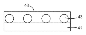
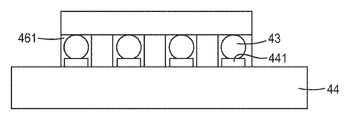
도 4a에 나타낸 바와 같이, 전자 구성요소(41) 또는 기판 상에 제1 반도체 패키지 수지 조성물(46)을 배치하는 단계는, 범프(43)가 제공된 전자 구성요소(41)의 표면 상에 제1 반도체 패키지 수지 조성물(46)을 전자 구성요소(41) 상의 범프들(43) 사이의 공간을 충전하도록 배치함으로써 실행될 수 있다.
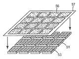
또한, 도 5a에 나타낸 바와 같이, 범프(53)가 제공된 개별적으로 분할된 전자 구성요소(51)의 표면 상에 제1 반도체 패키지 수지 조성물(56)이 인쇄된 지지체(57), 예를 들어, 이형 필름 또는 이형지를 적층하는 것이 가능하다. 도 5b에 나타낸 바와 같이, 범프(53)가 제공된 전자 구성요소(51)의 표면에 제1 반도체 패키지 수지 조성물(56)을 이송하는 것 또한 가능하다. 이러한 배치 방법에서는, 전자 구성요소(51)를 투명 지지체(57)로 적층하고, 수지 조성물(56)에 B-스테이지 전환을 적용하여 유동성이 제거되도록 지지체 측면을 광으로 조사한 후, 지지체(57)를 전자 구성요소(51)로부터 박리시킬 수 있다. 이러한 유형의 배치 방법을 사용함으로써, 개별적으로 분할된 전자 구성요소 상에 수지 조성물을 용이하게 배치할 수 있다.
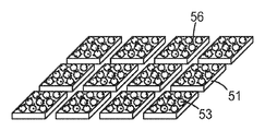
제1 반도체 패키지 수지 조성물(56)의 경화가 추가로 촉진되도록, 오븐과 같은 기구를 사용하여 전자 구성요소(51)를 가열하되, 최종 경화(겔화)가 일어나기 전에 반응을 중지한다. 도 5c에 나타낸 바와 같이, 이러한 방식으로 전자 구성요소(51)(범프(53)가 제공된 전자 구성요소의 표면 상에 형성된 수지 조성물(56)이 그 위에 경화되어 있음)를 기판(54)에 접촉 결합시킴으로써 반도체 패키지(500)를 제조하는 것이 가능하다.
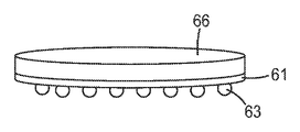
추가로, 제1 반도체 패키지 수지 조성물을 전자 구성요소 또는 기판 상에 배치하는 단계는, 도 6에 나타낸 바와 같이, 범프(63)가 제공되지 않은 전자 구성요소(61)의 표면에 제1 반도체 패키지 수지 조성물(66)을 적가한 후 스핀 코팅함으로써 실행할 수 있다. 세라믹 충전제(실리카, 알루미나 등)를 이러한 반도체 패키지 수지 조성물에 첨가함으로써, 열 전도성 수지 조성물을 얻고 전자 구성요소에 의해 발생되는 열을 외부로 발산하는 것이 가능하다.
일 실시 형태에서, 전자 구성요소 및/또는 기판 상에 배치된 제1 반도체 패키지 수지 조성물에 광을 이용한 조사를 적용하는 단계는, 도 3에 나타낸 바와 같이, 유출물(361)을 광으로 조사하는 상기 언급된 단계일 수 있다. 다른 실시 형태에서, 제1 반도체 패키지 수지에 광을 이용한 조사를 적용하는 단계는 또한, 도 2에 나타낸 바와 같이, 전자 구성요소(21) 및 기판(26) 상에 수지 조성물(24)을 오버코팅제로서 배치한 후, 수지 조성물(26) 전체를 광으로 조사함으로써 실행될 수 있다.
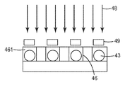
또한, 도 4a에 나타낸 바와 같이, 제1 반도체 패키지 수지 조성물(46)을 전자 구성요소(41) 상에 배치하고, 도 4b에 나타낸 바와 같이, 범프(43)가 광에 노출되지 않도록 하는 방식으로 마스크(49)를 위치시킨 후, 제1 반도체 패키지 수지 조성물(46)을 광(48)으로 조사하는 것이 가능하다. 마스킹된 범프(43)에서 수지 조성물에는 B-스테이지 전환이 적용되지 않고 유체로 남아 있으므로, 도 4c에 나타낸 바와 같이, 기판(44) 상에 배치될 때 기판(44)의 표면 상의 전극(441)과 범프(43) 사이에 양호한 전기적 접촉이 얻어진다.
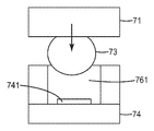
추가로, 도 7a에 나타낸 바와 같이, 제1 반도체 패키지 수지 조성물(76)을 기판(74) 상에 배치하고, 기판(74)의 표면 상의 전극(741)이 광에 노출되지 않도록 하는 방식으로 마스크(79)를 위치시킨 후, 제1 반도체 패키지 수지 조성물(76)을 광(78)으로 조사하는 것이 가능하다. 마스킹된 전극(741)에서 수지 조성물(761)에는 B-스테이지 전환이 적용되지 않고 유체로 남아 있으므로, 도 7b 및 도 7c에 나타낸 바와 같이, 전자 구성요소(71) 상에 배치될 때 전자 구성요소(71) 상의 전극(741)과 범프(73) 사이에 양호한 전기적 접촉이 얻어진다.
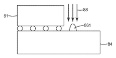
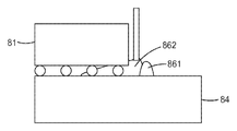
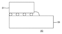
본 발명의 다른 실시 형태에서는, 도 8c에 나타낸 바와 같이, 전자 구성요소(81)와 기판(84)이 연결된 반도체 패키지가 제조된다. 이러한 반도체 패키지 제조 방법에서는, 도 8a에 나타낸 바와 같이, 전기적 구성요소(81) 및 기판(84)을 제조하고 기판(84)의 표면 상에 제1 반도체 패키지 수지 조성물(861)을 배치한다. 수지 조성물(861)을 배치하는 이 방법은 상기 언급된 다양한 방법 중 임의의 것일 수 있으나, 전자 구성요소(81)를 둘러싼 댐으로서 작용하도록 하는 방식으로 수지 조성물(861)을 배치한다.
그 다음에, 광(88)으로 조사함으로써 수지 조성물(861)에 B-스테이지 전환을 적용한 후, 도 8b에 나타낸 바와 같이, 제2 반도체 패키지 수지 조성물(862)을 기판(84)의 표면 상에 배치한다. 제2 반도체 패키지 수지 조성물(862) 또한 에폭시 수지, 경화제, 무기 입자, 및 광가교성 기를 함유하는 실란으로 표면 처리된 나노-입자를 함유한다. 최종 경화 후에 제1 반도체 패키지 수지 조성물과 대략 동일한 모듈, 열팽창 계수, 및 유리 전이점(Tg)을 얻기 위하여, 일 실시 형태에서 제2 반도체 패키지 수지 조성물(862)은 제1 반도체 패키지 수지 조성물(861)과 정확히 동일한 조성을 갖는다.
이어서, 최종 경화가 이루어지도록 제1 반도체 패키지 수지 조성물(861) 및 제2 반도체 패키지 수지 조성물(862)을 동시에 가열함으로써, 도 8c에 나타낸 반도체 패키지를 제조한다. 제1 반도체 패키지 수지 조성물(861) 및 제2 반도체 패키지 수지 조성물(862)을 별도로 가열할 수 있으나, 최종 경화 후에 거의 동일한 모듈, 열팽창 계수, 및 유리 전이점(Tg)을 달성하기 위하여, 바람직하게는 동시에 가열한다.
본 발명의 다른 실시 형태에서는, 도 9에 나타낸 바와 같이, 기판(94) 상에 배치된 반도체 패키지 수지 조성물(96) 상에 덮개(99)를 배치함으로써 얻어지는 반도체 패키지가 제조된다. 기판(94) 상에 마운팅된, 반도체 칩과 같은 전자 구성요소(91)를 둘러싸도록 하는 방식으로 반도체 패키지 수지 조성물(96)을 분배하고, 자외선 방사로 조사함으로써 B-스테이지 전환을 적용하고, 덮개(99)로 덮고, 수지 조성물(96)이 덮개(99)에 결합되도록 열 및 압력을 적용하고, 경화시킨다. 분배 및 자외선 방사 조사 단계를 수회 실행할 수 있으며, 수지 벽의 높이 또한 충분한 높이까지 증가시킬 수 있다.
실시예
본 발명은, 본 발명의 범주 내에 있는 많은 변형 및 변경이 당업자에게는 명백할 것이기 때문에 단지 예시로서 의도된 하기의 예에서 더욱 상세하게 설명된다. 달리 언급되지 않는다면, 하기 실시예에서 보고된 모든 부, 백분율, 및 비는 중량 기준이다.
반도체 패키지 수지 조성물의 제조에 사용된 구성요소를 표 1에 나타낸다.
[표 1]

나노 에폭시 20101104를 제조하기 위하여, 25.73 g의 3-(트라이메톡시실릴)프로필 메타크릴레이트(제품명 A174, 98% 3-(트라이메톡시실릴)프로필 메타크릴레이트, 알드리치(Aldrich)에 의해 제조) 및 0.5 g의 4-하이드록시-2,2,6,6-테트라메틸 피페리딘 1-옥실 자유 라디칼(도쿄 케미칼 인더스트리 컴퍼니 리미티드(Tokyo Chemical Industry Co., Ltd.)에 의해 제조)의 5 질량% 수용액을 450 g의 1-메톡시-2-프로판올에 첨가함으로써 액체를 먼저 제조하였다. 이어서, 액체를 400 g의 콜로이드성 실리카(제품명 O-40, 니산 케미칼 인더스트리스 리미티드(Nissan Chemical Industries, Ltd.)에 의해 제조, 고체 함량 40%)에 교반 중에 첨가하였다. 10 분 동안 교반한 후에, 16 시간 동안 80℃에서 액체를 가열함으로써 표면-개질된 나노-입자를 함유하는 반응 혼합물을 얻었다.
반응 혼합물을 주위 온도로 냉각시킨 후, 회전식 증발기를 사용하여 혼합물 중의 물을 제거하였다. 이어서, 200 g의 1-메톡시-2-프로판올을 액체에 첨가하고 증발기를 사용하여 임의의 잔류하는 물을 제거하였다. 이 단계를 2회 더 반복하여 실리카 나노-분산액을 얻었다. 이 실리카 나노-분산액에 1-메톡시-2-프로판올을 첨가함으로써 고체 함량을 대략 45 중량%로 조정하였다. 분산액으로부터 침강물을 제거하기 위하여 분산액을 1.0 ㎛ 유리 미세섬유 필터에 통과시켜, 1-메톡시-2-프로판올 중에 45 중량%의 A-174/실리카 나노-입자를 함유한 분산액을 얻었다.
비스페놀 A 유형 에폭시 수지와 비스페놀 F 유형 에폭시 수지의 혼합물(제품명 ZX1059, 니폰 스틸 케미칼 컴퍼니 리미티드에 의해 제조)을 나노-입자 분산액(고체 함량 45%)에 첨가하고 균질해질 때까지 교반하였다. 이어서, 회전식 증발기를 사용하여 1-메톡시-2-프로판올 용매를 완전히 제거하여, 광중합성 작용기를 함유하는 실란으로 표면 처리된 나노-입자의 에폭시 수지 분산액인 나노 에폭시 20101104(나노-입자 함량 33%)를 얻었다.
실시예 1, 비교예 A, 및 참고예 B
표 2에 나타낸 블렌딩 양을 사용하여, 구성요소들을 DAC 혼합기(모델명 AR-250, 씽키(Thinky)에 의해 제조)에 첨가하고 실온에서 3000 rpm으로 교반함으로써 블렌딩하여, 실시예 1, 비교예 A, 및 참고예 B의 반도체 패키지 수지 조성물을 얻었다.
[표 2]

반도체 패키지 수지 조성물의 평가
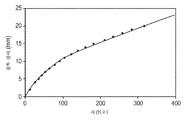
유동성
40 ㎛의 갭에 의해 분리된 2개의 유리 플레이트(상위 플레이트 30 × 30 ㎜, 하위 플레이트 40 × 40 ㎜) 사이에서 실시예 1의 반도체 패키지 수지 조성물의 침투 시간 및 길이를 측정하였다. 유리 플레이트를 100℃의 온도에서 열판 위에 위치시키고 반도체 패키지 수지 조성물을 상위 플레이트의 에지에 적용하였다. 상위 플레이트의 에지로부터 반도체 패키지 수지 조성물의 침투 길이 및 이러한 침투에 요구되는 시간을 측정하고 기록하였다. 그 결과가 도 10에 나타나 있다.
광경화
금속 마스크를 사용하여 50 × 50 ㎜ 인쇄 회로 기판(암 일렉트로닉스 컴퍼니 리미티드(Arm Electronics Co., Ltd.)에 의해 제조) 상에 실시예 1의 반도체 패키지 수지 조성물을 인쇄하였다. 인쇄를 실행할 때, 금속 마스크를 회로 기판 상에 위치시키고 마스크에 의해 덮이지 않은 회로 기판의 부분 위에만 조성물을 인쇄하였다. 이들 인쇄된 샘플 2개를 제조하고, 그 중의 하나를 저압 수은 증기 램프를 사용하여 500 Mj/㎠에서 자외선 방사로 조사하였다(샘플 a). 이어서, 양자 모두의 샘플을 120℃에서 60 분 동안 오븐 내에서 가열한 후, 오븐으로부터 꺼내어 촬영하였다. 그 결과가 도 11에 나타나 있다. 도 11에서 알 수 있는 바와 같이, 자외선 방사로 조사한 수지 조성물은 고온에서 감소된 유동성을 나타냈으며 인쇄 중에 원래 형상을 유지하였다.
실시예 1 및 참고예 B의 반도체 패키지 수지 조성물을 각각 유리 플레이트(30 × 30 ㎜)에 적용하고 그 위에 유리 플레이트(6 × 6 ㎜)를 위쪽으로부터 위치시켰다. 이어서, 저압 수은 증기 램프를 사용하여 500 Mj/㎠에서 유리 플레이트를 자외선 방사로 조사한 후, 30 초 동안 열판 위에서 250℃로 가열하였다. 경화 후에, 실시예 1의 샘플에서는 외부 균열이 나타나지 않았으나, 참고예 B의 샘플은 자외선 방사를 이용한 조사의 적용에 의해 과도하게 경화되었으므로 수지에 균열이 발생하였다.
최종 경화 후의 Tg, 탄성률, 및 열팽창 계수
저압 수은 증기 램프를 사용하여 500 Mj/㎠에서 실시예 1의 반도체 패키지 수지 조성물을 자외선 방사로 조사한 후, 165℃에서 2 시간 동안 최종 경화를 실행함으로써, UV를 동반하는 실시예 1의 샘플을 제조하였다. 자외선 방사로 조사하지 않고 165℃에서 2 시간 동안 실시예 1의 반도체 패키지 수지 조성물에 최종 경화를 적용함으로써, UV를 동반하지 않는 실시예 1을 사용하는 다른 샘플을 제조하였다. 저압 수은 증기 램프를 사용하여 500 Mj/㎠에서 비교예 A의 반도체 패키지 수지 조성물을 자외선 방사로 조사한 후, 165℃에서 2 시간 동안 최종 경화를 실행함으로써, UV를 동반하는 비교예 A를 사용하는 또 다른 샘플을 제조하였다. DMA 방법 및 25℃에서의 탄성률을 사용하여 이들 샘플의 유리 전이 온도(Tg)를 측정하였다.
DMA 방법을 사용하는 Tg 측정은 레오메트릭 사이언티픽에 의해 제조된 3점 곡선 모드의 고체 분석기(RSA-III)(변형률: 0.05%, 주파수: 1Hz)의 사용을 포함하였다. 샘플의 크기는 2 × 10 × 35 ㎣였고, 샘플은 3℃/분의 속도로 가열하였다. 비탄성률 측정은 3점 곡선 방법을 사용하였으며, 상기 언급된 장방형 샘플(크기: 2 × 10 × 35 ㎣)을 2개의 나이프 에지(25 ㎜ 분리됨) 상에 위치시키고 샘플의 중앙부를 내리눌러 샘플을 변형시키기 위해 사용된 하중을 측정하는 단계를 포함하였다. 이 경우에, 변형률은 0.05%의 최대값을 갖는 사인파로서 적용되었으며, 하중 또한 사인파로서 측정되었다(사인파의 주파수는 1 Hz였음). 그 측정 결과를 표 3에 나타내었다.
[표 3]

UV를 동반하는 실시예 1을 사용하는 샘플 및 UV를 동반하지 않는 실시예 1을 사용하는 샘플을 기재된 바와 동일한 방식으로 제조하였다. TMA 방법 및 열팽창 계수(CTE)를 사용하여 그들의 유리 전이 온도(Tg)를 측정하였다.
TMA 방법 및 CTE를 사용하여 Tg를 측정하는 경우, 리가쿠 코포레이션에 의해 제조된 TMA 8310 열역학적 분석 기구를 사용하였다. 질소 스트림 내에서 20℃/분의 속도로 샘플을 가열하였다. 압축 모드로 측정을 실행하였으며, 측정 중에 10 mN의 하중을 적용하였다. 샘플 길이를 온도의 함수로서 측정하였으며, 함수의 기울기로부터 열팽창 계수를 얻었다. 또한, 길이 대 온도를 플로팅하는 경우에 기울기가 최대인 온도로부터 Tg 값을 얻었다. 그 측정 결과가 표 4에 나타나 있다. α1 및 α2는 각각 Tg 값 미만 및 초과의 열팽창 계수이다.
[표 4]

UV를 동반하는 실시예 1을 사용하는 샘플 및 UV를 동반하지 않는 실시예 1을 사용하는 샘플을 상기와 동일한 방식으로 제조하고 DSC 방법을 사용하여 측정하였다.
퍼킨 엘머(PERKIN ELMER)에 의해 제조된 파이리스(Pyris) 1을 사용하여 DSC 측정을 실행하였으며, 온도를 10℃/min의 증가 속도로 50℃로부터 300℃까지 증가시킬 때 열량 대 온도의 플롯의 면적을 결정하고 ΔH로 표현하였다. 또한, 이 플롯의 피크 온도를 결정하였다. 결과는 표 5에 주어져 있다.
[표 5]

반도체 패키지의 제조
전자 구성요소(칩)(톱 라인(Top Line)에 의해 제조된 0.5 ㎜ 피치 플라스틱 BGA) 및 5 ㎜ × 5 ㎜ 기판(암 일렉트로닉스 컴퍼니 리미티드에 의해 제조)을 제조하고, 분배기(dispenser)를 사용하여 기판의 표면에 실시예 1의 반도체 패키지 수지 조성물을 적용하였다. 플립 칩 본더(flip chip bonder)(니폰 아비오닉스 컴퍼니 리미티드(Nippon Avionics Co., Ltd.)에 의해 제조된 MB-4500)를 사용하는 광학 유닛을 이용하여 기판 및 칩의 위치를 식별하고 칩 상의 솔더 볼(solder ball)이 기판 상의 랜드(land)와 정렬되도록 하는 방식으로 열적으로 접촉 결합시킴으로써 기판 상에 칩을 마운팅하였다. 이어서, 자외선 램프(도시바 코포레이션(Toshiba Corporation)에 의해 제조된 FL10BL)를 사용하여 300 초 동안 자외선 방사로 조사함으로써 반도체 패키지 수지 조성물의 에지에 B-스테이지 전환을 적용하였다. 150℃에서 2 시간 동안 오븐 내에서 가열하여 반도체 패키지 수지 조성물에 최종 경화를 적용함으로써 반도체 패키지를 얻었다. 다이아몬드 블레이드를 사용하여 이 반도체 패키지의 단면을 절단하고 촬영하였다. 그 사진이 도 12에 나타나 있다.
반도체 패키지 수지 조성물의 에지에 B-스테이지 전환을 적용함으로써, 최종 경화 중에 고온에 노출된 경우에도 반도체 칩의 위치가 이동하지 않았다. 또한, B-스테이지 전환에 요구되는 시간은 극히 짧았으며, 즉, 300 초였다.
본 발명은 바람직한 실시 형태들을 참조하여 설명되었지만, 당업자는 본 발명의 사상 및 범주로부터 벗어남이 없이 형태 및 상세 사항에 있어서 변경이 이루어질 수 있음을 인식할 것이다.≪ 1 >
1 is a cross-sectional view of a prior art semiconductor package.
2,
2 is a cross-sectional view of a prior art semiconductor package having an overmolding agent.
3,
3 is a cross-sectional view of a semiconductor package manufactured using the semiconductor package manufacturing method according to the embodiment of the present invention.
4A,
4A is a schematic cross-sectional view of steps of a method of manufacturing a semiconductor package according to an embodiment of the present invention, in which a semiconductor package resin composition is disposed on an electronic component.
4 (b)
4B is a schematic cross-sectional view of steps of a method of manufacturing a semiconductor package according to an embodiment of the present invention, in which irradiation with light is applied to a part of the semiconductor package resin composition.
4C,
4C is a schematic cross-sectional view of steps of a method of manufacturing a semiconductor package according to an embodiment of the present invention, wherein the electronic component is in contact with the substrate.
5A)
5A is a schematic view of steps of a method of manufacturing a semiconductor package according to an embodiment of the present invention in which a support on which a semiconductor package resin composition is printed is laminated on a wafer provided with a bump.
5B,
Figure 5b is a schematic view of a wafer according to an embodiment of the present invention in which a bump is provided and a first semiconductor package resin composition is disposed thereon.
5C)
5C is a schematic view of steps of a method of manufacturing a semiconductor package according to an embodiment of the present invention, wherein the wafer is contact bonded to a substrate after B-stage switching of the semiconductor package resin composition.
6,
6 is a view of an electronic component according to an embodiment of the present invention in which a semiconductor package resin composition is disposed on a surface not provided with a bump.
7a)
7A is a schematic cross-sectional view of steps of a method of manufacturing a semiconductor package according to an embodiment of the present invention, in which B-stage conversion by irradiation with light is applied to a semiconductor package resin composition.
7B,
7B is a schematic cross-sectional view of steps of a method of manufacturing a semiconductor package according to an embodiment of the present invention, wherein the electronic component is in contact with the substrate.
7C,
7C is a cross-sectional view of a semiconductor package manufactured by using the semiconductor package manufacturing method according to the embodiment of the present invention.
8A,
8A is a schematic cross-sectional view of steps of a method of manufacturing a semiconductor package according to an embodiment of the present invention in which a first semiconductor package resin composition is disposed on a surface of a substrate.
8B,
8B is a schematic cross-sectional view of steps of a method of manufacturing a semiconductor package according to an embodiment of the present invention, in which a second semiconductor package resin composition is disposed on a surface of a substrate.
8C)
8C is a cross-sectional view of a semiconductor package manufactured using the semiconductor package manufacturing method according to the embodiment of the present invention.
9,
9 is a cross-sectional view of a semiconductor package manufactured by using the semiconductor package manufacturing method according to the embodiment of the present invention.
<Fig. 10>
10 is a graph showing the fluidity of the semiconductor package resin composition according to the embodiment of the present invention.
11)
11 is a graph showing the photocurability of the semiconductor package resin composition according to the embodiment of the present invention.
12,
12 is a photograph showing a cross section of a semiconductor package manufactured by using the semiconductor package manufacturing method according to the embodiment of the present invention.
DETAILED DESCRIPTION OF THE INVENTION [
All numbers are herein considered to be modified by the term "about ". References to numerical ranges by endpoints include all numbers contained within that range (e.g., 1 to 5 include 1, 1.5, 2, 2.75, 3, 3.80, 4, and 5). All parts referred to herein are by weight unless otherwise indicated.
Suitable epoxy resins for use in the semiconductor package resin compositions of the present invention include, but are not limited to, aliphatic, alicyclic, aromatic, or heterocyclic monomeric, or oligomeric epoxy compounds. Generally, these materials have on average at least one polymerizable epoxy group per molecule and may have at least 1.5 or at least two polymerizable epoxy groups per molecule. In a given mode, it is possible to use a multifunctional epoxy compound having three or four polymerizable epoxy groups per molecule. The epoxy compound may be a pure compound or a mixture of compounds containing one, two, or more epoxy groups per molecule.
The above-mentioned epoxy compounds may have any type of backbone and may contain substituents. Examples of suitable substituents include, but are not limited to, halogen, ester groups, ethers, sulfonate groups, siloxane groups, nitro groups, phosphate groups and the like. The epoxy equivalent value of the epoxy compound can generally be varied within the range of 50 to 2000.
Examples of oligomeric epoxy compounds include linear oligomers having terminal epoxy groups (e.g., diglycidyl ethers of polyoxyalkylene glycols), oligomers having skeletal epoxy units (e.g., polybutadiene poly Or an oligomer having a pendant epoxy group (e.g., glycidyl methacrylate oligomer or co-oligomer).
In a predetermined mode, it is possible to use a glycidyl ether monomer represented by the following formula.
In the above formula, R is a radical having a valence of n, and n is an integer of 1 to 6. R can be an aromatic group, an alicyclic group, an aliphatic group, or a combination thereof. Typical epoxy compounds include glycidyl ethers of polyhydric phenols obtained by reacting polyhydric phenols with chlorohydrin such as excess epichlorohydrin (e.g., 2,2-bis- (2,3-epoxypropoxyphenol ) -Propane). ≪ / RTI > In particular, it is possible to use aromatic epoxy compounds, alicyclic epoxy compounds, aliphatic epoxy compounds, and the like.
Suitable aromatic epoxy compounds include, but are not limited to, diglycidyl ether of bisphenol A (bisphenol A type epoxy resin), diglycidyl ether of bisphenol F (bisphenol F type epoxy resin), 4,4'-dihydroxybiphenyl di Glycidyl ether, oligomers of these diglycidyl ethers, polyglycidyl ether of cresol novolak resin (cresol novolak type epoxy resin), and polyglycidyl ether of phenol novolac resin (phenol novolac type epoxy Resin). ≪ / RTI >
Exemplary alicyclic epoxy compounds include, but are not limited to, compounds obtained by hydrogenating the above-mentioned aromatic epoxy compounds, for example, hydrogenated bisphenol A type epoxy compounds and hydrogenated bisphenol F type epoxy compounds. Also, compounds containing a cyclohexene oxide group such as vinylcyclohexene monoxide, 1,2-epoxy-4-vinylcyclohexane, 1,2: 8,9-diepoxy limonene, 3,4- Hexenyl methyl-3 ', 4'-epoxycyclohexene carboxylate, and epoxy cyclohexanecarboxylate, such as 3,4-epoxycyclohexenylmethyl-3,4-epoxycyclohexanecarboxylate, The use of 3,4-epoxy-2-methylcyclohexylmethyl-3,4-epoxy-2-methylcyclohexanecarboxylate and bis (3,4-epoxy-6-methylcyclohexylmethyl) adipate It is possible.
Suitable aliphatic epoxy compounds include but are not limited to glycidyl ethers of aliphatic polyhydric alcohols or their alkylene oxide adducts. For example, there may be mentioned ethylene glycol diglycidyl ether, di (ethylene glycol) diglycidyl ether, propylene glycol diglycidyl ether, tri (propylene glycol) diglycidyl ether, neopentyl glycol diglycidyl ether , 1,4-butanediol diglycidyl ether, 1,6-hexanediol diglycidyl ether, trimethylol propane triglycidyl ether, trimethylol propane diglycidyl ether, poly (ethylene Glycol) diglycidyl ether, and the like.
In addition to the above-mentioned epoxy resin, it is possible to use a halogenated epoxy resin (for example, a brominated bisphenol type epoxy resin) or an epoxy compound having a glycidylamino group. The epoxy compound having a glycidylamino group is an epoxy compound (epoxy resin) obtained by epoxidizing an amine through the action of an epihalohydrin, and examples thereof include an aminophenol type epoxy resin, triglycidyl isocyanurate, Tetraglycidyl diaminodiphenylmethane, tetraglycidyl meta-xylenediamine, and hexaglycidyl triaminobenzene.
Aminophenol type epoxy resins are obtained by epoxidation of aminophenols using methods known to those skilled in the art. Examples of aminophenols are 2-aminophenol, 3-aminophenol, 4-aminophenol, 2-amino-m-cresol, 2-amino-p-cresol, -Cresol, and aminophenols such as 6-amino-m-cresol and aminocresol.
Other epoxy resins suitable for use include copolymers of acrylic esters of glycidol (e.g., glycidyl acrylate and glycidyl methacrylate) with one or more copolymerizable vinyl compounds. This type of copolymer includes styrene-glycidyl methacrylate and methyl methacrylate-glycidyl acrylate copolymers. It is also possible to use epoxy-functional silicon, which is a polydimethylsiloxane in which the silicon atom is replaced by an epoxy alkyl group.
Among the above-mentioned epoxy resins, the use of a bisphenol A type epoxy resin, a bisphenol F type epoxy resin, or an aminophenol type epoxy resin is preferable from the viewpoint of characteristics after final curing of the semiconductor package resin composition. Also, in view of obtaining a balance between the viscosity of the semiconductor package resin composition and the properties after the final curing, it is preferable to add both the bisphenol A type epoxy resin and the bisphenol F type epoxy resin or the bisphenol A type epoxy resin and the bisphenol F type epoxy resin to the aminophenol type It is preferable to use a three-component system obtained by further adding an epoxy resin. Specifically, the product ZX1059 (a mixture of bisphenol A and bisphenol F manufactured by Nippon Steel Chemical Co., Ltd.) or an aminophenol type epoxy jER (registered trademark) 630 (manufactured by Mitsubishi Chemical Co., Ltd.) Chemical Corporation), both of which are commercially available.
The blending amount of the epoxy resin is generally 50 mass% or less with respect to the total amount of the semiconductor package resin composition, and 10 to 40 mass% in some modes.
The curing agent contained in the semiconductor package resin composition of the present invention may be a curing agent conventionally used for thermosetting an epoxy compound. Specific examples thereof include an amino compound, an acid anhydride compound, an amide compound, a phenol compound, a boron trifluoride complex compound such as BF 3 -monoethanolamine, imidazole such as 2-ethyl-4-methyl But are not limited to, imidazole, hydrazide, such as, for example, amino dihydrazide, guanidine, such as tetramethylguanidine, and dicyanamide. The curing agent may be a single curing agent or a mixture of different curing agents. From the viewpoint of viscosity, an acid anhydride compound is preferable.
It is suitable to use non-aromatic acid anhydride compounds. For example, there can be mentioned hexahydrophthalic anhydride, 3-methylhexahydrophthalic anhydride, 4-methylhexahydrophthalic anhydride, 1-methylnorbornane-2,3-dicarboxylic acid anhydride, 5-methylnorbornane- , 3-dicarboxylic acid anhydride, norbornane-2,3-dicarboxylic acid anhydride, 1-methylnadic anhydride, 5-methylnadic anhydride, nadic anhydride, tetrahydrophthalic anhydride, Hydrofluoric anhydride, 4-methyl tetrahydrophthalic anhydride, dodecenylsuccinic anhydride, and the like.
Among them, hexahydrophthalic anhydride having no double bond, 3-methylhexahydrophthalic anhydride, 4-methylhexahydrophthalic anhydride, 1-methylnorbornane-2,3-dicarboxylic anhydride, 5- Methyl norbornane-2,3-dicarboxylic anhydride, or norbornane-2,3-dicarboxylic anhydride are particularly suitable. A mixture of 4-methylhexahydrophthalic anhydride and hexahydrophthalic anhydride (for example, a mixture of Rikacid MH-700 (4-methyl (meth) acrylate) prepared by New Japan Chemical Co., Hexahydrophthalic anhydride / hexahydrophthalic anhydride ratio = 70/30)) is particularly suitable since the semiconductor package resin composition containing this mixture has a low viscosity and is hardly crystallized.
Exemplary phenolic hardeners are bisphenol A, bisphenol F, bisphenol S, 4,4'-biphenyl phenol, tetramethyl bisphenol A, dimethyl bisphenol A, tetramethyl bisphenol F, dimethyl bisphenol F, tetramethyl bisphenol S, (4-hydroxyphenyl) -2- [4-phenyl] propane, 2,2-dimethylphenol, (3-methyl-6-tert-butylphenol), trishydroxyphenylmethane, resorcinol-4'- Hydroquinone, pyrogallol, diisopropylidene, phenols having a terpene skeleton, phenols having a fluorene skeleton such as 1,1-di-4-hydroxyphenylfluorene, phenolated polybutadiene , Phenol, cresol, ethylphenol, butylphenol, octylphenol, and novolac resins such as bisphenol A, bisphenol F, bisphenol S, naphthol, terpene diphenol, etc. A novolak resin obtained by using the same phenol as a raw material, a phenol novolac resin having a xylylene skeleton, a phenol novolac resin having a dicyclopentadienes skeleton, a phenol novolac resin having a biphenyl skeleton, Phenol novolak resins, and phenol novolac resins having a furan skeleton.
Exemplary amino-based curing agents include, but are not limited to, aliphatic amines such as diethylenetriamine, triethylenetetramine, or tetraethylenepentamine, aromatic amines such as diaminodiphenylmethane, - xylenediamine, and condensation products of aromatic amines and aldehydes, polyamidoamines.
From the viewpoint of the properties of the resulting cured product, the blending amount of the curing agent is approximately the same as the blending amount of the epoxy resin. Generally, the blending amount of the curing agent is from 5 to 15 mass% based on the total weight of the semiconductor package resin composition.
The inorganic particles are dispersed substantially homogeneously in the semiconductor package resin composition of the present invention. It is possible to use a single type or a combination of two or more types of inorganic particles to impart a high modulus of elasticity and a low thermal expansion coefficient to the semiconductor package resin composition. In general, these inorganic particles may be selected from the group consisting of silica (fused silica, crystalline silica), alumina, calcium silicate, calcium carbonate, potassium titanate, silicon carbide, silicon nitride, aluminum nitride, boron nitride, beryllium, zirconia, zircon, Powder such as talc, spinel, mullite, or titania, beads obtained by sphering these powders, glass fiber, or the like. It is possible to use these inorganic particles in a single type or in a combination of two or more types.
Of the above-mentioned inorganic particles, fused silica is particularly suitable from the viewpoint of thermal expansion characteristics, and crystalline silica and alumina are particularly suitable from the viewpoint of having high thermal conductivity. In addition, when silica particles are produced as inorganic particles from an organic sol, since the particle size distribution thereof is narrow, it is possible to effectively distribute the particles in the resin composition. Further, the shape of the primary particles of the inorganic particles is not particularly important, but spherical particles are preferable from the viewpoint of being able to flow and penetrate into the fine gaps.
In addition, from the viewpoint of the fluidity of the semiconductor package resin composition, the inorganic particles have a small average particle diameter and a narrow particle size distribution. The inorganic particles used in the present invention have an average particle diameter of 10 mu m or less because the inorganic particles tend to be accumulated when the semiconductor package resin composition is pushed into the narrow gap. In one embodiment, the average particle diameter of the inorganic particles is in particular not more than 5 占 퐉, more particularly not more than 3 占 퐉, still more particularly not more than 2 占 퐉. However, the lower limit of the average particle diameter of the inorganic particles is not particularly limited, but from the viewpoint of flowability, the average particle diameter is 0.05 mu m or more in the case of silica particles and 0.1 mu m or more in the case of alumina particles. In one embodiment, the particle diameter of the inorganic particles in the semiconductor package resin composition is in the range of "average particle diameter 占 (average particle diameter 占 0.3)" (for example, 1 占 0.3 占 퐉). The average particle diameter and the particle size distribution of the inorganic particles can be measured by an electron microscope or a laser scattering apparatus. Further, the inorganic particles can be surface-treated to such an extent that the dispersibility of the particles in the resin composition is not impaired.
The silica particles prepared by the sol-gel method and having a narrow particle size distribution are particularly suitable as inorganic particles and have an average particle diameter of 0.8 to 1.8 mu m which is produced by the sol-gel method and has a particle size distribution (average particle diameter & Average particle diameter x 0.3)) is even more suitable. These inorganic particles can be prepared by, for example, silica KE-S150 and KE-S10 (manufactured by Nippon Shokubai Co., Ltd. using a sol-gel method), silica HPS-1000 (Prepared using a sol-gel method by Toagosei Co., Ltd.) or silica SS-07, SS-10 and SS-14 (manufactured by Tokuyama Corporation, sol- ). ≪ / RTI >
The semiconductor package resin composition of the present invention contains nano-particles surface-treated with a silane containing a photopolymerizable functional group. Exposure to light (e. G., Ultraviolet radiation and / or visible light), so that irradiation for a short period of time (several seconds to tens of seconds) and B-stage conversion It is possible to adjust the fluidity of the resin composition.
In general, these nano-particles may be selected from the group consisting of silica (e.g. fused silica or crystalline silica), alumina, calcium silicate, calcium carbonate, potassium titanate, silicon carbide, silicon nitride, aluminum nitride, boron nitride, beryllium, zirconia, zircon, Powders such as forsterite, stearate, spinel, mullite, or titania, beads obtained by sphering these powders, glass fibers, and the like. It is possible to use these inorganic particles in a single type or in a combination of two or more types.
Among nano-particles, silica particles are particularly suitable from the viewpoint of chemical stability, and alumina is preferable from the viewpoint of thermal conductivity. In addition, when silica particles are produced as nano-particles from an organic sol, since the particle size distribution thereof is narrow, it is possible to effectively distribute the particles in the resin composition. Also, although the shape of the nano-particles is not particularly important, spherical particles are particularly suitable from the viewpoint of being able to flow and penetrate into a fine gap.
The average particle diameter of the nano-particles suitable for use in the composition of the present invention is in the range of 1 nm to less than 1 占 퐉. In order to improve the reactivity of the photopolymerizable functional group, the average particle diameter of the nano-particles is preferably small. In general, the average particle diameter of the nano-particles may be between 5 nm and 500 nm, in particular between 10 nm and 300 nm, more particularly between 10 nm and 100 nm.
The functional group that can be polymerized by light is CH2= CH-C (= O) -O- group, CH2= CCH3A -C (= O) -O- group, a glycidyl group, a vinyl group and the like.
The silane containing photopolymerizable functional groups may be selected from the group consisting of 3- (trimethoxysilyl) propyl methacrylate, vinyltrimethoxysilane, vinyltriethoxysilane, p-styryltrimethoxysilane, or (meth) For example, 3-methacryloxypropyltrimethoxysilane, 3-methacryloxypropyltrimethoxysilane, methyldimethoxysilane, or 3-acryloxypropyltrimethoxysilane. They can be bound to the surface of the nano-particles by chemical bonding (covalent bonding or ionic bonding) or by strong physical bonding.
Way
Nano-particles surface-treated with silane containing photopolymerizable functional groups can be prepared, for example, using the following method.
A liquid is prepared by adding a silane containing a photopolymerizable functional group to a solvent, and then the liquid is added to the colloidal silica under agitation. After stirring, the mixture is heated at an elevated temperature for 10 to 20 hours to obtain a reaction mixture containing surface-modified nano-particles.
The reaction mixture is then cooled to ambient temperature and water is removed from the mixture by means of a rotary evaporator. The solvent is then added and any remaining water is removed by evaporator (this step may be repeated several times). Subsequently, a solvent is added to the reaction mixture to adjust the solid content therein. The reaction mixture dispersion is then filtered through a 1.0 micron glass microfiber filter to remove the precipitate and obtain a dispersion containing the nanocomposite treated with silane containing photopolymerizable functional groups in the solvent.
The amount of the nano-particles surface-treated with the silane containing the inorganic particles and the photopolymerizable functional group in the semiconductor package resin composition is 60% by mass or more with respect to the total amount of the semiconductor package resin composition from the viewpoint of the thermal expansion coefficient of the obtained cured object, From the viewpoint of viscosity of the resin composition, 90% by mass or less with respect to the total amount of the semiconductor package resin composition. When the blending amount of the inorganic particles falls within this range, it is generally possible to obtain a cured product having a thermal expansion coefficient of 35 ppm or less, and it is also possible to use the semiconductor package resin composition of the present invention as a semiconductor package resin composition.
The amount of the nano-particles surface-treated with the silane containing a photopolymerizable functional group is 0.1% by mass or more and 10% by mass or less based on the total amount of the nano-particles and the inorganic particles. In performing B-stage conversion, the amount of nano-particles added is adjusted to obtain the desired viscosity (flowability) of the resin composition. If the amount of the nano-particles surface-treated with the silane containing a photopolymerizable functional group is too small, it is impossible to adjust the viscosity (fluidity) of the resin composition even when irradiated with light, and if the amount is too large, And shrinkage upon curing occurs during thermal curing after irradiation with light, and cracks appear in the cured product.
It is particularly preferable to add a photopolymerization initiator to the semiconductor package resin composition of the present invention. Examples of the photopolymerization initiator include benzoin, benzoin methyl ether, benzoin ethyl ether, benzoin n-propyl ether, benzoin n-butyl ether, benzyl, benzophenone, p-methylbenzophenone, diacetyl, But are not limited to, echine, thionine, Michler's ketone, acetophenone, 2-chlorothioxanthone, anthraquinone, chloroanthraquinone, 2-methyl anthraquinone, Hydroxy-1-cyclohexyl acetophenone, 2,2-dimethoxy-2-phenylacetophenone, methylbenzoin Methyl-1- [4- (methylthio) phenyl] -2-morpholinophene, dichlorothioxanthone, diisopropylthioxanthone, phenyl disulfide-2-nitrosofluorene, Cyclohexanone, cyclohexanone, cyclohexanone, cyclohexanone, cyclohexanone, cyclohexanone, cyclohexanone, cyclohexanone, And the like is not one which limits. One or more of its types can be used.
The organic titanium compound can be added to the semiconductor package resin composition. The organic titanium compound may have a hydrolyzable group or a hydrophobic group in the compound. Such organotitanium compounds are generally known as titanium coupling agents. The organic titanium compound reacts with the -OH group on the surface of the inorganic particles and forms a covalent bond with titanium, for example, by removing the alcohol by hydrolysis. Without wishing to be bound by theory, it is believed that this will organize the surface of the inorganic particles and cause good dispersibility of the inorganic particles in the epoxy resin.
The hydrolysable group in the organic compound is, for example, ROneO-, -O-CH2-CH2-O-, or -O-CH2-C (= O) -O-, and the like. Here, ROneMay be a substituted or unsubstituted, straight or branched chain alkyl group, an alkenyl group, an aryl group, or an aralkyl group. After reaction with the inorganic particles, ROneIs removed (e.g., removed by forming an alcohol), it is preferable that after removal R1 is a group having a somewhat lower boiling point. Therefore, a particularly suitable ROneIs a substituted or unsubstituted, straight or branched chain alkyl group having a number of carbon atoms, especially 1 to 10 carbon atoms (more particularly 1 to 8 carbon atoms).
Further, the hydrophobic group in the organic titanium compound is -O-C (= O) -R2, -O-S (= O)2-Ph-R2, -O-P (= O) (-OH) -O-P (= O) - (OR2)2, -O-P (= O) - (OR2)2, HO-P- (OR2)2, -O- (CH2) m-NH- (CH2) n-NH2 And so on. Wherein Ph represents a phenyl group, m and n each represent an integer of 1 to 10, R2May be a substituted or unsubstituted, straight or branched chain alkyl group, an alkenyl group, an aryl group, or an aralkyl group. In order to improve the efficiency of covering the surface of the inorganic particles, R2Especially a group having a plurality of carbon atoms, more particularly a substituted or unsubstituted, linear or branched alkyl group having 8 to 30 carbon atoms.
Of these, -O-C (= O) -R2, HO-P- (OR2)2, And -O- (CH2) m-NH- (CH2) n-NH2Is a hydrophobic group particularly suitable in view of the reactivity with the inorganic particles in the semiconductor package resin composition and the reduced viscosity of the semiconductor package resin composition. From the viewpoint of fluidity, -O-C (= O) -R2 Or HO-P- (OR2)2From the viewpoint of stability of the titanium coupling agent, -O-C (= O) -R2Is more appropriate. Here, R2Quot; is a substituted or unsubstituted, linear or branched alkyl group having 8 to 30 carbon atoms, preferably 10 to 30 carbon atoms.
Specifically, the titanium coupling agent may be, for example, tetraalkoxy titanium (for example, tetraethoxy titanium, tetraisopropoxy titanium or tetrabutoxy titanium), tetra (ethylene glycol) titanate, di- But are not limited to, butyl bis (triethanolamine) titanate, di-isopropoxy bis (acetylacetonate) titanium, isopropoxytitanium octanoate, isopropyl titanium trimethacrylate, isopropyl titanium triacrylate, (Isopropyl tributyl (meth) acrylate, isopropyl tributyl (meth) acrylate, stearyl titanate, isopropyl tributyl benzenesulfonyl titanate, isopropyl tributyl (butyl, methyl pyrophosphate) titanate, , Diacryloxyacetate titanate, die (da Octylphosphite) ethylene titanate, isopropoxytitanium tri (dioctylphosphate), isopropyl tris (dioctyl pyrophosphate) titanate, tetraisopropyl bis (dioctyl phosphite) titanate, tetraoctyl bis (di- (Di-tridecylphosphite) titanate, bis (dioctylpyrophosphate) oxyacetate titanate, tris (di-tridecylphosphite) titanate, Isopropyl triisooctanoyl titanate, isopropyl triisooctanoyl titanate, isopropyl diisopropenyl titanate, isopropyl triisooctyl titanate, isopropyl triisooctanoyl titanate, isopropyl diisopropenyl titanate, Diacrylic titanate, isopropyltri (dioctylphosphate) titanate Agent, isopropyl tri-cumyl phenyl titanate, isopropyl tri (N- aminoethyl-aminoethyl) titanate and the like.
KRTTS (isopropyl triisostearoyl titanate (CH (CH3) 2), available from Ajinomoto Fine-Techno Co., Inc., Plenact (R) series sold by Ajinomoto Fine-3)2CHOTi [OCO (CH2)14CH (CH3)2]3), KR 46B (tetraoctylbis (di-tridecylphosphite) titanate), KR 55 (tetra (2,2-diallyloxymethyl-1-butyl) bis (di-tridecyl) phosphite titanate) , KR 38S (isopropyl tris (dioctyl pyrophosphate) titanate), KR 138S (bis (dioctyl pyrophosphate) oxyacetate titanate), KR 41B (tetraisopropyl bis (dioctyl pyrophosphate) titanate) (Isopropyl tributylphosphate) ethylenetitanate), KR38S (tris (dioctylpyrophosphate) ethylene titanate), KR38 (isopropyldioxypyrophosphate titanate), KR44 Tris (dodecylbenzylphenyl) titanate), and the like. PLELECT KR TTS, KR 46B, and KR 9SA are suitable, PLELECT KR TTS and KR 46B are more suitable.
From the viewpoint of reducing the viscosity of the semiconductor package resin composition, the blending amount of the organic titanium compound is 1% by mass or more, particularly 2% by mass or more, more particularly 2.5% by mass or more, based on the total amount of the semiconductor package resin composition. However, in view of the reduced glass transition temperature and the modulus of elasticity of the resulting cured product, the blending amount of the organotitanium compound is not more than 5 mass%, especially not more than 4 mass%, more particularly not more than 3 mass%, based on the total amount of the semiconductor package resin composition.
Of the organic phosphoric acid compounds, phosphoric acid esters which can be used in the semiconductor package resin composition of the present invention include, but are not limited to, esters obtained by applying dehydrocondensation to phosphoric acid and alcohol. By additionally adding a phosphoric acid ester to the above-mentioned organic titanium compound, the phosphoric acid ester forms a weak bond with titanium, for example, a coordination bond. As a result, the depth of the organic layer on the surface of the inorganic particles which are organized by the organic titanium compound increases.
Specifically, phosphoric acid esters are phosphoric acid (O-P (OH)3Has a structure in which some or all of the three hydrogen atoms in the hydrogen atom are replaced by an organic group. Compounds in which one, two, and three hydrogen atoms are replaced are phosphoric acid monoesters (P (OZ)3), Phosphoric acid diesters (HOP (OZ)2), And phosphoric acid triester ((HO)2POZ). Here, Z represents a substituted or unsubstituted alkyl group having 10 to 50 carbon atoms, a phenyl group, a polyester, or a polycaprolactone. From the viewpoint of increasing the thickness of the organic layer formed on the surface of the inorganic particles, Z has a particularly high molecular weight. Especially a weight average molecular weight of 200 to 20,000, and more particularly 300 to 10,000.
Such as, for example, dimethyl phosphate, diethyl phosphate, dipropyl phosphate, monobutyl phosphate, dibutyl phosphate, mono-2-ethylhexyl phosphate, di-2-ethylhexyl phosphate, monophenyl phosphate, mono-2-ethylhexyl Phosphite, dioctyl phosphate, diphenyl phosphate and the like can be used as the above-mentioned compounds. Suitable commercially available products include, but are not limited to, Disperbyk 111, manufactured by BYK Chemicals of Japan.
Of the above-mentioned phosphate esters, phosphoric acid esters are particularly suitable in view of dispersion of the inorganic particles, and phosphate esters in which Z is polycaprolactone are more particularly suitable.
From the viewpoint of reducing the viscosity of the semiconductor package resin composition, the blending amount of the phosphoric acid ester is 0.5% by mass or more, particularly 1% by mass or more, more particularly 1.2% by mass or more, based on the total amount of the semiconductor package resin composition. However, from the viewpoint of causing a decrease in the electrical characteristics (insulation property) of the resulting cured product, the blending amount of the phosphoric acid ester is preferably 3% by mass or less, particularly 2% by mass or less, more preferably 1.8% % Or less.
As described above, it is possible to improve the dispersibility of the inorganic particles in the epoxy resin and improve the fluidity of the resulting semiconductor package resin composition by combining the organotitanium compound with the phosphate ester. Specifically, R3OTi (OCOR4H)3 Or (R3O)4Ti [HOP (OR4)2] Wherein R3Represents a straight or branched chain alkyl group having from 3 to 8 carbon atoms and R4Quot; refers to a straight or branched chain alkyl group having from 10 to 20 carbon atoms), an organotitanium compound having a weight average molecular weight of from 200 to 20,000 and a HOP (OZ)2(Wherein Z represents a substituted or unsubstituted alkyl group having from 10 to 50 carbon atoms, a phenyl group, a polyester, or a polycaprolactone) is particularly suitable. Do.
In addition to the above-mentioned components, the semiconductor package resin composition of the present invention may also contain a reaction accelerator. Here, the reaction promoter used for promoting the reaction between the epoxy resin and the curing agent may be a reaction promoter known to those skilled in the art, for example, a cyclamidine compound, a tertiary amine, a quaternary ammonium salt, an imidazole, Organic phosphorus compounds such as organophosphines, for example, triphenylphosphine, or derivatives thereof, or tetraphenylboron salts. A single reaction promoter or a combination of two or more types thereof may be used. In addition, as long as the reaction promoting effect is achieved, the amount of the blend of the reaction promoter is not particularly limited.
In addition, in order to improve moisture resistance and high-temperature exposure characteristics of a semiconductor device, it is possible to blend an ion capturing agent in the semiconductor package resin composition of the present invention. The ion trapping agent is not particularly limited, and it is possible to use any ion trapping agent known to those skilled in the art. In particular, hydrotalcite or hydrous oxides of elements such as magnesium, aluminum, titanium, zirconium, or bismuth can be used.
In addition, it is possible to use a stress relaxing agent such as a silicone rubber powder, a dye, a colorant such as carbon black, a smoothing agent, a defoaming agent, and other inorganic fillers (for example, , For example, aluminum hydroxide, magnesium hydroxide, zinc silicate, or zinc molybdate) may be blended into the semiconductor package resin composition of the present invention at a level that does not compromise the object of the present invention. In addition, it is also possible to use compounds of the general formula (I) in which R < 1 > is a phosphorous acid, a phosphoric acid ester, a melamine, a melamine derivative, a compound having a triazine ring, a nitrogen-containing compound such as a cyanuric acid derivative or an isocyanuric acid derivative, Antimony trioxide, antimony trioxide, antimony tetroxide, and antimony pentoxide, and flame retardants, such as, for example, brominated epoxies, such as, for example, Resins and the like can also be blended into the semiconductor package resin composition of the present invention.
As long as the above-mentioned components can be uniformly dispersed and blended, any type of manufacturing method can be used to produce the semiconductor package resin composition of the present invention. Typical manufacturing methods involve blending or separately blending, mixing and dissolving a certain amount of blended raw materials and blending these components during heating and cooling, if necessary, in a mixing roller, extruder, planetary mixer, And dispersing, then cooling and, if necessary, bubbling and crushing. It is also possible to first prepare a mixture of all the components except for the inorganic particles, and then add inorganic particles to the mixture to obtain a semiconductor package resin composition. In addition, if required, it is also possible to form the semiconductor package resin composition into tablets having appropriate dimensions and weight for molding conditions.
The semiconductor package resin composition of the present invention can be sufficiently cured by photopolymerization so that B-stage conversion can be effected (i. E., Sufficient curing is performed to soften the composition without melting when heated).
In one embodiment, the final cured product of the semiconductor package resin composition of the present invention has a thermal expansion coefficient of 10 to 35 ppm. Since silicon has a low coefficient of thermal expansion, it is preferable that the material used to seal the silicon when sealing the semiconductor also has a low thermal expansion coefficient. If the coefficient of thermal expansion exceeds 35 ppm, cracks may occur due to thermal stress. It is also possible to measure the coefficient of thermal expansion using TMA (Thermal Mechanical Analyzer). Specifically, it is possible to measure the coefficient of thermal expansion with the TMA 8310 thermodynamic analysis instrument manufactured by Rigaku Corporation. The sample (size: 4 x 5 x 10 cm) is heated in a nitrogen stream at a rate of 20 캜 / min, a load of 10 mN is applied, and the measurement is performed in a compressed mode.
In one embodiment, the final cured product of the semiconductor package resin composition of the present invention has a glass transition temperature (Tg) of 60 to 120 캜 and an elastic modulus (dynamic storage modulus, E ') of 5 to 40 GPa. The glass transition temperature and elastic modulus can be measured using a DMA (dynamic mechanical analysis) instrument. This measurement method was performed using a three-point curve mode solid-state analyzer (RSA-III) (strain: 0.05%, frequency: 1 Hz) manufactured by Rheometric Scientific and a sample heated at a rate of 3 DEG C / (Size: 2 x 10 x 35 mm).
Specifically, by placing the above-mentioned rectangular sample (size: 2 x 10 x 35 mm) on two knife edges (separated by 25 mm) and lowering the center of the sample to measure the load usage to deform the sample, It is possible to measure the elastic modulus (dynamic storage modulus) using a point curve method. In this case, the strain is applied as a sine wave having a maximum value of 0.05%, and the load is also measured as a sine wave (sine wave frequency is 1 Hz).
Method of manufacturing a semiconductor package
In one embodiment, the present invention provides a process for preparing a nanocomposite comprising: (1) providing an electronic component and / or a substrate; (2) providing a nano-particle surface treated with a silane containing an epoxy resin, a curing agent, (3) a B-stage switching step of irradiating part or all of the first semiconductor package resin composition with light, and (4) a step of heating the semiconductor package resin composition And curing the first semiconductor package resin composition. The semiconductor package manufacturing method of the present invention can be used to connect electronic components to other electronic components or to connect electronic components to a substrate.
In one embodiment of the present invention, as shown in Fig. 3, a semiconductor package to which the
When the first semiconductor
The light used for the irradiation may be light in any wavelength range capable of causing photopolymerization of the resin composition, for example, ultraviolet radiation or visible light. The light source may be a low pressure, medium pressure, or high pressure mercury vapor lamp, laser, xenon flash lamp, and the like.
The final curing is performed by heating the first semiconductor
In general, the final curing is carried out by heating at a temperature of 120 DEG C or higher and 200 DEG C or lower for a period of 10 minutes to 3 hours. During this step, the glycidyl group in the epoxy resin reacts with the curing agent. This type of cured product has a three-dimensionally cross-linked chemical structure.
4A, the step of disposing the first semiconductor
5A, a
The
In addition, the step of disposing the first semiconductor package resin composition on the electronic component or the substrate may include the step of disposing the first semiconductor package resin composition on the surface of the
In one embodiment, the step of applying light irradiation to the first semiconductor package resin composition disposed on the electronic component and / or the substrate comprises the step of irradiating the
4A, the first semiconductor
7A, the first semiconductor
In another embodiment of the present invention, as shown in Fig. 8C, a semiconductor package to which the
After the B-stage conversion is applied to the
Subsequently, the first semiconductor
In another embodiment of the present invention, as shown in Fig. 9, a semiconductor package obtained by disposing a
Example
The present invention is described in further detail in the following examples, which are intended as illustrations only, since many variations and modifications within the scope of the present invention will be apparent to those skilled in the art. Unless otherwise stated, all parts, percentages, and ratios reported in the following examples are by weight.
The components used in the production of the semiconductor package resin composition are shown in Table 1.
[Table 1]
To prepare nano-epoxy 20101104, 25.73 g of 3- (trimethoxysilyl) propyl methacrylate (product name A174, 98% 3- (trimethoxysilyl) propyl methacrylate, manufactured by Aldrich) And 0.5 g of 4-hydroxy-2,2,6,6-tetramethylpiperidine 1-oxyl free radical (manufactured by Tokyo Chemical Industry Co., Ltd.) % Aqueous solution was added to 450 g of 1-methoxy-2-propanol. The liquid was then added to 400 g of colloidal silica (trade name O-40, manufactured by Nissan Chemical Industries, Ltd., solid content 40%) during stirring. After stirring for 10 minutes, the liquid was heated at 80 占 폚 for 16 hours to obtain a reaction mixture containing the surface-modified nano-particles.
After cooling the reaction mixture to ambient temperature, water in the mixture was removed using a rotary evaporator. Then 200 g of 1-methoxy-2-propanol was added to the liquid and any residual water was removed using an evaporator. This step was repeated two more times to obtain a silica nano-dispersion. The solids content was adjusted to approximately 45% by weight by adding 1-methoxy-2-propanol to the silica nano-dispersion. To remove the precipitate from the dispersion, the dispersion was passed through a 1.0 micron glass microfibre filter to obtain a dispersion containing 45 wt% A-174 / silica nano-particles in 1-methoxy-2-propanol.
A mixture of bisphenol A type epoxy resin and bisphenol F type epoxy resin (product name ZX1059, manufactured by Nippon Steel Chemical Co., Ltd.) was added to the nano-particle dispersion (solid content 45%) and stirred until homogeneous. Subsequently, the 1-methoxy-2-propanol solvent was completely removed using a rotary evaporator to obtain a nano-epoxy resin dispersion solution of nano-particles 20101104 (nano-particle content 33%), which was surface treated with silane containing photopolymerizable functional groups. ).
Example One, Comparative Example A, and Reference example B
Using the amounts of blending shown in Table 2, the components were blended by adding to a DAC mixer (model name AR-250, manufactured by Thinky) and stirring at 3000 rpm at room temperature to yield Example 1, Comparative A, And the semiconductor package resin composition of Reference Example B were obtained.
[Table 2]
Evaluation of semiconductor package resin composition
liquidity
The penetration time and length of the semiconductor package resin composition of Example 1 were measured between two glass plates (upper plate 30 占 30 mm, lower plate 40 占 40 mm) separated by a gap of 40 占 퐉. The glass plate was placed on a hot plate at a temperature of 100 DEG C and the semiconductor package resin composition was applied to the edge of the upper plate. The penetration length of the semiconductor package resin composition from the edge of the upper plate and the time required for such penetration were measured and recorded. The results are shown in Fig.
Photocuring
The semiconductor package resin composition of Example 1 was printed on a 50 x 50 mm printed circuit board (manufactured by Arm Electronics Co., Ltd.) using a metal mask. When performing printing, the composition was printed only on the portion of the circuit board where the metal mask was placed on the circuit board and not covered by the mask. Two of these printed samples were prepared and one of them was irradiated with ultraviolet radiation at 500 Mj /
The semiconductor package resin compositions of Example 1 and Reference Example B were each applied to a glass plate (30 × 30 mm), and a glass plate (6 × 6 mm) was placed thereon from above. Subsequently, the glass plate was irradiated with ultraviolet radiation at 500 Mj / cm < 2 > using a low pressure mercury vapor lamp, and then heated to 250 DEG C on a hot plate for 30 seconds. After curing, no external cracks were observed in the sample of Example 1, but the sample of Reference Example B was excessively cured by application of irradiation using ultraviolet radiation, so that cracks occurred in the resin.
Tg, elastic modulus, and thermal expansion coefficient after final curing
A sample of Example 1 with UV irradiation was prepared by irradiating the semiconductor package resin composition of Example 1 with ultraviolet radiation at 500 Mj /
The Tg measurement using the DMA method included the use of a three point curved mode solid analyzer (RSA-III) (strain: 0.05%, frequency: 1 Hz) manufactured by Rheometric Scientific. The size of the sample was 2 x 10 x 35 mm, and the sample was heated at a rate of 3 ° C / min. The non-elasticity ratio was measured using a three-point curve method. The rectangular sample (size: 2 x 10 x 35 mm) was placed on two knife edges (separated by 25 mm) And measuring the load used to make it. In this case, the strain was applied as a sine wave having a maximum value of 0.05%, and the load was also measured as a sine wave (the frequency of the sine wave was 1 Hz). The measurement results are shown in Table 3.
[Table 3]
Samples using Example 1 with UV and Example 1 without UV were prepared in the same manner as described. Their glass transition temperature (Tg) was measured using TMA method and thermal expansion coefficient (CTE).
When measuring the Tg using the TMA method and the CTE, the TMA 8310 thermodynamic analysis instrument manufactured by Rigaku Corporation was used. The sample was heated at a rate of 20 [deg.] C / min in a nitrogen stream. The measurement was performed in the compression mode and a load of 10 mN was applied during the measurement. The sample length was measured as a function of temperature and the thermal expansion coefficient was obtained from the slope of the function. Further, in the case of plotting the length versus temperature, the Tg value was obtained from the temperature at which the slope was maximum. The measurement results are shown in Table 4. alpha 1 and
[Table 4]
Samples using Example 1 with UV and Example 1 without UV were prepared in the same manner as above and measured using the DSC method.
DSC measurements were performed using Pyris 1 manufactured by PERKIN ELMER and the area of the plot of the caloric value versus temperature when increasing the temperature from 50 ° C to 300 ° C at an increasing rate of 10 ° C / Was determined and expressed as? H. The peak temperature of the plot was also determined. The results are given in Table 5.
[Table 5]
Manufacturing of semiconductor packages
Electronic components (chips) (0.5 mm pitch plastic BGA manufactured by Top Line) and 5 mm by 5 mm substrates (manufactured by Arm Electronics Co., Ltd.) were manufactured and dispensers were used The semiconductor package resin composition of Example 1 was applied to the surface of the substrate. The position of the substrate and the chip is identified by using an optical unit using a flip chip bonder (MB-4500 manufactured by Nippon Avionics Co., Ltd.) The chip was mounted on the substrate by thermal contact bonding in such a way that the solder balls were aligned with the land on the substrate. Subsequently, B-stage conversion was applied to the edge of the semiconductor package resin composition by irradiation with ultraviolet radiation for 300 seconds using an ultraviolet lamp (FL10BL manufactured by Toshiba Corporation). A semiconductor package was obtained by heating in an oven at 150 DEG C for 2 hours to apply final curing to the semiconductor package resin composition. A section of this semiconductor package was cut and photographed using a diamond blade. The photograph is shown in Fig.
By applying B-stage switching to the edge of the semiconductor package resin composition, the position of the semiconductor chip did not move even when exposed to high temperatures during final curing. Also, the time required for B-stage switching was extremely short, i.e., 300 seconds.
While the present invention has been described with reference to preferred embodiments, those skilled in the art will recognize that changes may be made in form and detail without departing from the spirit and scope of the invention.
Claims (9)
경화제;
무기 입자;
광중합성 작용기를 함유하는 실란으로 표면 처리된 나노-입자; 및
광중합 개시제를 포함하는 반도체 패키지 수지 조성물.Epoxy resin;
Curing agent;
Inorganic particles;
Nano-particles surface-treated with silane containing photopolymerizable functional groups; And
A semiconductor package resin composition comprising a photopolymerization initiator.
제1 반도체 패키지 수지 조성물을 전자 구성요소 및/또는 기판 상에 배치하는 단계(여기서, 반도체 패키지 수지 조성물은 에폭시 수지, 경화제, 무기 입자, 및 광가교성 기를 함유하는 실란으로 표면 처리된 나노-입자를 포함함);
B-스테이지 전환(B-stage conversion) 중에 제1 반도체 패키지 수지 조성물의 적어도 일부를 광으로 조사하는 단계; 및
가열에 의해 제1 반도체 패키지 수지 조성물을 경화시키는 단계를 포함하는, 반도체 패키지의 제조 방법.Providing at least one of an electronic component and a substrate;
Disposing a first semiconductor package resin composition on an electronic component and / or a substrate, wherein the semiconductor package resin composition comprises a nano-particle surface treated with a silane containing an epoxy resin, a curing agent, an inorganic particle and a photo- );
Irradiating at least a portion of the first semiconductor package resin composition with light during B-stage conversion (B-stage conversion); And
And curing the first semiconductor package resin composition by heating.
제2 반도체 패키지 수지 조성물을 전자 구성요소 및/또는 기판 상에 배치하는 단계(여기서, 제2 반도체 패키지 수지 조성물은 에폭시 수지, 경화제, 무기 입자, 및 광가교성 기를 함유하는 실란으로 표면 처리된 나노-입자를 함유함); 및
가열에 의해 제2 반도체 패키지 수지 조성물을 경화시키는 단계를 추가로 포함하는 방법.6. The method of claim 5,
Placing a second semiconductor package resin composition on an electronic component and / or a substrate, wherein the second semiconductor package resin composition comprises an epoxy resin, a curing agent, an inorganic particle, and a silane-treated nano- Containing particles); And
And curing the second semiconductor package resin composition by heating.
Applications Claiming Priority (3)
| Application Number | Priority Date | Filing Date | Title |
|---|---|---|---|
| US201161508344P | 2011-07-15 | 2011-07-15 | |
| US61/508,344 | 2011-07-15 | ||
| PCT/US2012/045916 WO2013012587A2 (en) | 2011-07-15 | 2012-07-09 | Semiconductor package resin composition and usage method thereof |
Publications (1)
| Publication Number | Publication Date |
|---|---|
| KR20140058557A true KR20140058557A (en) | 2014-05-14 |
Family
ID=47558664
Family Applications (1)
| Application Number | Title | Priority Date | Filing Date |
|---|---|---|---|
| KR1020147003608A KR20140058557A (en) | 2011-07-15 | 2012-07-09 | Semiconductor package resin composition and usage method thereof |
Country Status (5)
| Country | Link |
|---|---|
| US (2) | US9230873B2 (en) |
| JP (2) | JP6155261B2 (en) |
| KR (1) | KR20140058557A (en) |
| TW (1) | TWI550018B (en) |
| WO (1) | WO2013012587A2 (en) |
Families Citing this family (9)
| Publication number | Priority date | Publication date | Assignee | Title |
|---|---|---|---|---|
| US20140011052A1 (en) * | 2011-03-28 | 2014-01-09 | 3M Innovative Properties Company | Curable composition, article, method of curing, and reaction product |
| JP6271164B2 (en) * | 2013-06-17 | 2018-01-31 | 日立オートモティブシステムズ株式会社 | Box-type in-vehicle controller |
| KR102186491B1 (en) | 2014-01-02 | 2020-12-03 | 헨켈 아이피 앤드 홀딩 게엠베하 | Film containing nano-particulate filler |
| US9220183B1 (en) * | 2014-07-16 | 2015-12-22 | International Business Machines Corporation | Devices employing semiconductor die having hydrophobic coatings, and related cooling methods |
| JP6872313B2 (en) * | 2015-10-13 | 2021-05-19 | リンテック株式会社 | Semiconductor devices and composite sheets |
| WO2017122717A1 (en) * | 2016-01-12 | 2017-07-20 | 日立化成株式会社 | Photosensitive resin composition, dry film using same, printed wiring board, and method for manufacturing printed wiring board |
| JP7454906B2 (en) * | 2016-10-14 | 2024-03-25 | 株式会社レゾナック | Underfill material, electronic component device, and method for manufacturing electronic component device |
| JP7218378B2 (en) * | 2018-02-19 | 2023-02-06 | シグニファイ ホールディング ビー ヴィ | Sealed device with light engine |
| JP7109940B2 (en) * | 2018-03-08 | 2022-08-01 | 日東電工株式会社 | Sealing adhesive sheet |
Family Cites Families (20)
| Publication number | Priority date | Publication date | Assignee | Title |
|---|---|---|---|---|
| US6228681B1 (en) | 1999-03-10 | 2001-05-08 | Fry's Metals, Inc. | Flip chip having integral mask and underfill providing two-stage bump formation |
| US6245595B1 (en) | 1999-07-22 | 2001-06-12 | National Semiconductor Corporation | Techniques for wafer level molding of underfill encapsulant |
| US6281046B1 (en) | 2000-04-25 | 2001-08-28 | Atmel Corporation | Method of forming an integrated circuit package at a wafer level |
| US6573122B2 (en) | 2001-03-28 | 2003-06-03 | International Rectifier Corporation | Wafer level insulation underfill for die attach |
| US6794761B2 (en) | 2001-04-26 | 2004-09-21 | Intel Corporation | No-flow underfill material |
| US20030111519A1 (en) | 2001-09-04 | 2003-06-19 | 3M Innovative Properties Company | Fluxing compositions |
| EP1302514B1 (en) | 2001-10-09 | 2009-07-15 | Mitsubishi Chemical Corporation | Active energy ray-curable antistatic coating composition |
| US20030162911A1 (en) | 2002-01-31 | 2003-08-28 | Yue Xiao | No flow underfill composition |
| US20060194064A1 (en) | 2002-03-01 | 2006-08-31 | Xiao Allison Y | Underfill encapsulant for wafer packaging and method for its application |
| US20060147719A1 (en) | 2002-11-22 | 2006-07-06 | Slawomir Rubinsztajn | Curable composition, underfill, and method |
| US7022410B2 (en) | 2003-12-16 | 2006-04-04 | General Electric Company | Combinations of resin compositions and methods of use thereof |
| US20040101688A1 (en) * | 2002-11-22 | 2004-05-27 | Slawomir Rubinsztajn | Curable epoxy compositions, methods and articles made therefrom |
| KR100774798B1 (en) | 2004-05-13 | 2007-11-07 | 닛토덴코 가부시키가이샤 | Epoxy resin composition for semiconductor encapsulation and semiconductor device using the same |
| EP1950239B1 (en) | 2005-10-28 | 2017-01-04 | Sumitomo Osaka Cement Co., Ltd. | Transparent inorganic-oxide dispersion, resin composition containing inorganic oxide particles, composition for encapsulating luminescent element, luminescent element, hard coat, optical functional film, optical part, and process for producing resin composition containing inorganic oxide particles |
| JP2008180992A (en) * | 2007-01-25 | 2008-08-07 | Hitachi Chem Co Ltd | Photosensitive resin composition, photosensitive film for permanent resist, resist pattern forming method, printed wiring board and semiconductor package |
| CN101657891A (en) | 2007-03-13 | 2010-02-24 | 洛德公司 | Convex die attachment method |
| JP2008297373A (en) | 2007-05-29 | 2008-12-11 | Somar Corp | Underfill material comprising liquid epoxy resin composition, and flip chip type semiconductor device |
| JP5004351B2 (en) | 2007-11-30 | 2012-08-22 | 信越化学工業株式会社 | Manufacturing method of semiconductor device |
| WO2010098636A2 (en) | 2009-02-27 | 2010-09-02 | 주식회사 엘지화학 | Outstandingly abrasion resistant and pollution resistant coating composition and coating film |
| WO2010138440A1 (en) * | 2009-05-26 | 2010-12-02 | 3M Innovative Properties Company | Process for making filled resins |
-
2012
- 2012-07-09 KR KR1020147003608A patent/KR20140058557A/en not_active Application Discontinuation
- 2012-07-09 US US14/131,827 patent/US9230873B2/en not_active Expired - Fee Related
- 2012-07-09 WO PCT/US2012/045916 patent/WO2013012587A2/en active Application Filing
- 2012-07-09 JP JP2014520234A patent/JP6155261B2/en not_active Expired - Fee Related
- 2012-07-13 TW TW101125423A patent/TWI550018B/en not_active IP Right Cessation
-
2015
- 2015-07-28 US US14/810,631 patent/US9773714B2/en not_active Expired - Fee Related
-
2017
- 2017-03-08 JP JP2017043422A patent/JP2017133023A/en active Pending
Also Published As
| Publication number | Publication date |
|---|---|
| TWI550018B (en) | 2016-09-21 |
| TW201311806A (en) | 2013-03-16 |
| US20140217622A1 (en) | 2014-08-07 |
| JP2014524957A (en) | 2014-09-25 |
| US9230873B2 (en) | 2016-01-05 |
| US20150329740A1 (en) | 2015-11-19 |
| US9773714B2 (en) | 2017-09-26 |
| WO2013012587A3 (en) | 2013-04-18 |
| WO2013012587A2 (en) | 2013-01-24 |
| JP2017133023A (en) | 2017-08-03 |
| JP6155261B2 (en) | 2017-06-28 |
Similar Documents
| Publication | Publication Date | Title |
|---|---|---|
| US9773714B2 (en) | Semiconductor package resin composition and usage method thereof | |
| JP4892164B2 (en) | Liquid epoxy resin composition and electronic component device | |
| JPH10212395A (en) | Resin composition and semiconductor device produced by using the same | |
| JP6233441B2 (en) | Liquid epoxy resin composition and electronic component device | |
| JP5664220B2 (en) | Semiconductor sealing material and semiconductor device | |
| JP2015193851A (en) | Liquid epoxy resin composition and electronic part device | |
| WO2018221681A1 (en) | Liquid resin composition for sealing and electronic component device | |
| JP2005054045A (en) | Epoxy resin molding compound for sealing use and electronic component device | |
| KR20190133564A (en) | Epoxy resin composition for encapsulating semiconductor device and semiconductor device encapsulated using the same | |
| JP2009057575A (en) | Liquid epoxy resin composition and electronic component device | |
| JP6657716B2 (en) | Liquid composition for sealing, sealing material, and electronic component device | |
| JP5523816B2 (en) | Modified resin composition, method for producing the same, and curable resin composition containing the same | |
| WO2012018684A1 (en) | Encapsulating resin composition | |
| JP2005171209A (en) | Filler-containing resin composition and its production method | |
| JP5708666B2 (en) | Liquid epoxy resin composition and electronic component device | |
| JP2016040393A (en) | Liquid epoxy resin composition, and electronic component device | |
| JP2015180760A (en) | Liquid epoxy resin composition and electronic part device | |
| CN114402029A (en) | Sealing material for compression molding and electronic component device | |
| JP2015110803A (en) | Liquid epoxy resin composition and electronic part device | |
| JP5664358B2 (en) | Epoxy resin composition, semiconductor sealing material, and semiconductor device | |
| JP5924443B2 (en) | Liquid epoxy resin composition and electronic component device | |
| JP5929977B2 (en) | Liquid epoxy resin composition and electronic component device | |
| KR101293791B1 (en) | Epoxy resin composition for encapsulating semiconductor device and semiconductor device using the same | |
| KR102549224B1 (en) | Epoxy Resin Composition for Sealing Semiconductor | |
| JP5804479B2 (en) | Manufacturing method of resin-encapsulated semiconductor device and resin-encapsulated semiconductor device |
Legal Events
| Date | Code | Title | Description |
|---|---|---|---|
| A201 | Request for examination | ||
| E902 | Notification of reason for refusal | ||
| E601 | Decision to refuse application |