KR20140012073A - 나노구조 어레이를 위한 전극 구조 및 이의 제조 방법 - Google Patents
나노구조 어레이를 위한 전극 구조 및 이의 제조 방법 Download PDFInfo
- Publication number
- KR20140012073A KR20140012073A KR1020137022698A KR20137022698A KR20140012073A KR 20140012073 A KR20140012073 A KR 20140012073A KR 1020137022698 A KR1020137022698 A KR 1020137022698A KR 20137022698 A KR20137022698 A KR 20137022698A KR 20140012073 A KR20140012073 A KR 20140012073A
- Authority
- KR
- South Korea
- Prior art keywords
- contact layer
- contact
- nanowires
- another example
- nanowire
- Prior art date
- Legal status (The legal status is an assumption and is not a legal conclusion. Google has not performed a legal analysis and makes no representation as to the accuracy of the status listed.)
- Withdrawn
Links
Images


Classifications
-
- H—ELECTRICITY
- H10—SEMICONDUCTOR DEVICES; ELECTRIC SOLID-STATE DEVICES NOT OTHERWISE PROVIDED FOR
- H10N—ELECTRIC SOLID-STATE DEVICES NOT OTHERWISE PROVIDED FOR
- H10N10/00—Thermoelectric devices comprising a junction of dissimilar materials, i.e. devices exhibiting Seebeck or Peltier effects
- H10N10/80—Constructional details
- H10N10/85—Thermoelectric active materials
-
- H—ELECTRICITY
- H10—SEMICONDUCTOR DEVICES; ELECTRIC SOLID-STATE DEVICES NOT OTHERWISE PROVIDED FOR
- H10D—INORGANIC ELECTRIC SEMICONDUCTOR DEVICES
- H10D62/00—Semiconductor bodies, or regions thereof, of devices having potential barriers
- H10D62/10—Shapes, relative sizes or dispositions of the regions of the semiconductor bodies; Shapes of the semiconductor bodies
- H10D62/117—Shapes of semiconductor bodies
- H10D62/118—Nanostructure semiconductor bodies
- H10D62/119—Nanowire, nanosheet or nanotube semiconductor bodies
- H10D62/122—Nanowire, nanosheet or nanotube semiconductor bodies oriented at angles to substrates, e.g. perpendicular to substrates
-
- B—PERFORMING OPERATIONS; TRANSPORTING
- B82—NANOTECHNOLOGY
- B82Y—SPECIFIC USES OR APPLICATIONS OF NANOSTRUCTURES; MEASUREMENT OR ANALYSIS OF NANOSTRUCTURES; MANUFACTURE OR TREATMENT OF NANOSTRUCTURES
- B82Y10/00—Nanotechnology for information processing, storage or transmission, e.g. quantum computing or single electron logic
-
- H—ELECTRICITY
- H10—SEMICONDUCTOR DEVICES; ELECTRIC SOLID-STATE DEVICES NOT OTHERWISE PROVIDED FOR
- H10D—INORGANIC ELECTRIC SEMICONDUCTOR DEVICES
- H10D62/00—Semiconductor bodies, or regions thereof, of devices having potential barriers
- H10D62/10—Shapes, relative sizes or dispositions of the regions of the semiconductor bodies; Shapes of the semiconductor bodies
- H10D62/17—Semiconductor regions connected to electrodes not carrying current to be rectified, amplified or switched, e.g. channel regions
- H10D62/213—Channel regions of field-effect devices
- H10D62/221—Channel regions of field-effect devices of FETs
-
- H—ELECTRICITY
- H10—SEMICONDUCTOR DEVICES; ELECTRIC SOLID-STATE DEVICES NOT OTHERWISE PROVIDED FOR
- H10N—ELECTRIC SOLID-STATE DEVICES NOT OTHERWISE PROVIDED FOR
- H10N10/00—Thermoelectric devices comprising a junction of dissimilar materials, i.e. devices exhibiting Seebeck or Peltier effects
- H10N10/80—Constructional details
- H10N10/81—Structural details of the junction
-
- H—ELECTRICITY
- H10—SEMICONDUCTOR DEVICES; ELECTRIC SOLID-STATE DEVICES NOT OTHERWISE PROVIDED FOR
- H10N—ELECTRIC SOLID-STATE DEVICES NOT OTHERWISE PROVIDED FOR
- H10N10/00—Thermoelectric devices comprising a junction of dissimilar materials, i.e. devices exhibiting Seebeck or Peltier effects
- H10N10/80—Constructional details
- H10N10/85—Thermoelectric active materials
- H10N10/851—Thermoelectric active materials comprising inorganic compositions
- H10N10/855—Thermoelectric active materials comprising inorganic compositions comprising compounds containing boron, carbon, oxygen or nitrogen
-
- H—ELECTRICITY
- H10—SEMICONDUCTOR DEVICES; ELECTRIC SOLID-STATE DEVICES NOT OTHERWISE PROVIDED FOR
- H10N—ELECTRIC SOLID-STATE DEVICES NOT OTHERWISE PROVIDED FOR
- H10N10/00—Thermoelectric devices comprising a junction of dissimilar materials, i.e. devices exhibiting Seebeck or Peltier effects
- H10N10/80—Constructional details
- H10N10/85—Thermoelectric active materials
- H10N10/851—Thermoelectric active materials comprising inorganic compositions
- H10N10/8556—Thermoelectric active materials comprising inorganic compositions comprising compounds containing germanium or silicon
-
- H—ELECTRICITY
- H10—SEMICONDUCTOR DEVICES; ELECTRIC SOLID-STATE DEVICES NOT OTHERWISE PROVIDED FOR
- H10N—ELECTRIC SOLID-STATE DEVICES NOT OTHERWISE PROVIDED FOR
- H10N10/00—Thermoelectric devices comprising a junction of dissimilar materials, i.e. devices exhibiting Seebeck or Peltier effects
- H10N10/80—Constructional details
- H10N10/85—Thermoelectric active materials
- H10N10/857—Thermoelectric active materials comprising compositions changing continuously or discontinuously inside the material
Landscapes
- Chemical & Material Sciences (AREA)
- Inorganic Chemistry (AREA)
- Engineering & Computer Science (AREA)
- Nanotechnology (AREA)
- Physics & Mathematics (AREA)
- Mathematical Physics (AREA)
- Theoretical Computer Science (AREA)
- Crystallography & Structural Chemistry (AREA)
- Powder Metallurgy (AREA)
- Measuring Temperature Or Quantity Of Heat (AREA)
Applications Claiming Priority (5)
| Application Number | Priority Date | Filing Date | Title |
|---|---|---|---|
| US201161438709P | 2011-02-02 | 2011-02-02 | |
| US61/438,709 | 2011-02-02 | ||
| US13/331,768 | 2011-12-20 | ||
| US13/331,768 US20120152295A1 (en) | 2010-12-21 | 2011-12-20 | Arrays of filled nanostructures with protruding segments and methods thereof |
| PCT/US2012/023425 WO2012161757A1 (en) | 2011-02-02 | 2012-02-01 | Electrode structures for arrays of nanostructures and methods thereof |
Publications (1)
| Publication Number | Publication Date |
|---|---|
| KR20140012073A true KR20140012073A (ko) | 2014-01-29 |
Family
ID=47217566
Family Applications (1)
| Application Number | Title | Priority Date | Filing Date |
|---|---|---|---|
| KR1020137022698A Withdrawn KR20140012073A (ko) | 2011-02-02 | 2012-02-01 | 나노구조 어레이를 위한 전극 구조 및 이의 제조 방법 |
Country Status (7)
| Country | Link |
|---|---|
| EP (1) | EP2671255A4 (enExample) |
| JP (1) | JP2014510396A (enExample) |
| KR (1) | KR20140012073A (enExample) |
| CN (1) | CN103460387A (enExample) |
| BR (1) | BR112013019766A2 (enExample) |
| CA (1) | CA2825888A1 (enExample) |
| WO (1) | WO2012161757A1 (enExample) |
Families Citing this family (9)
| Publication number | Priority date | Publication date | Assignee | Title |
|---|---|---|---|---|
| AU2013212087A1 (en) | 2012-01-25 | 2014-08-07 | Alphabet Energy, Inc. | Modular thermoelectric units for heat recovery systems and methods thereof |
| US9257627B2 (en) | 2012-07-23 | 2016-02-09 | Alphabet Energy, Inc. | Method and structure for thermoelectric unicouple assembly |
| US9065017B2 (en) | 2013-09-01 | 2015-06-23 | Alphabet Energy, Inc. | Thermoelectric devices having reduced thermal stress and contact resistance, and methods of forming and using the same |
| CN103579484A (zh) * | 2013-11-05 | 2014-02-12 | 姚芸 | 一种温差发电器用金属导体电极 |
| TWI570972B (zh) * | 2016-01-20 | 2017-02-11 | 財團法人工業技術研究院 | 熱電轉換裝置以及熱電轉換器 |
| JP6830587B2 (ja) * | 2016-04-11 | 2021-02-17 | 学校法人東京理科大学 | 導電膜付き柱状インゴット基板及びその製造方法、シリサイド系熱電変換素子及びその製造方法、熱電変換モジュール、並びにシリサイド系熱電変換素子の電極層形成用組成物 |
| WO2019003581A1 (ja) * | 2017-06-27 | 2019-01-03 | 株式会社村田製作所 | 熱電変換モジュールおよび電子部品モジュール |
| WO2019003582A1 (ja) * | 2017-06-27 | 2019-01-03 | 株式会社村田製作所 | 熱電変換モジュールおよび電子部品モジュール |
| KR102265762B1 (ko) * | 2019-11-27 | 2021-06-15 | 한국세라믹기술원 | 적외선 차단 투명전극 점착제 및 이를 이용한 스마트 윈도우 |
Family Cites Families (14)
| Publication number | Priority date | Publication date | Assignee | Title |
|---|---|---|---|---|
| JP3600486B2 (ja) * | 1999-08-24 | 2004-12-15 | セイコーインスツル株式会社 | 熱電変換素子の製造方法 |
| TW554388B (en) * | 2001-03-30 | 2003-09-21 | Univ California | Methods of fabricating nanostructures and nanowires and devices fabricated therefrom |
| US8154093B2 (en) * | 2002-01-16 | 2012-04-10 | Nanomix, Inc. | Nano-electronic sensors for chemical and biological analytes, including capacitance and bio-membrane devices |
| JP2004031696A (ja) * | 2002-06-26 | 2004-01-29 | Kyocera Corp | 熱電モジュール及びその製造方法 |
| US20050060884A1 (en) * | 2003-09-19 | 2005-03-24 | Canon Kabushiki Kaisha | Fabrication of nanoscale thermoelectric devices |
| US6969679B2 (en) * | 2003-11-25 | 2005-11-29 | Canon Kabushiki Kaisha | Fabrication of nanoscale thermoelectric devices |
| US8039726B2 (en) * | 2005-05-26 | 2011-10-18 | General Electric Company | Thermal transfer and power generation devices and methods of making the same |
| WO2008060282A1 (en) * | 2006-11-17 | 2008-05-22 | General Electric Company | Thermal transfer and power generation devices and methods of making the same |
| US8049203B2 (en) * | 2006-12-22 | 2011-11-01 | Qunano Ab | Nanoelectronic structure and method of producing such |
| US20080178920A1 (en) * | 2006-12-28 | 2008-07-31 | Schlumberger Technology Corporation | Devices for cooling and power |
| US7905013B2 (en) * | 2007-06-04 | 2011-03-15 | Sharp Laboratories Of America, Inc. | Method for forming an iridium oxide (IrOx) nanowire neural sensor array |
| JP4925964B2 (ja) * | 2007-08-06 | 2012-05-09 | 株式会社デンソー | 積層型熱電変換素子及びその製造方法 |
| FR2923601B1 (fr) * | 2007-11-12 | 2010-01-01 | Commissariat Energie Atomique | Detecteur de rayonnement electromagnetique a connexion par nanofil et procede de realisation |
| TWI401830B (zh) * | 2008-12-31 | 2013-07-11 | Ind Tech Res Inst | 低熱回流之熱電奈米線陣列及其製造方法 |
-
2012
- 2012-02-01 CN CN2012800167545A patent/CN103460387A/zh active Pending
- 2012-02-01 EP EP12790253.4A patent/EP2671255A4/en not_active Withdrawn
- 2012-02-01 KR KR1020137022698A patent/KR20140012073A/ko not_active Withdrawn
- 2012-02-01 CA CA2825888A patent/CA2825888A1/en not_active Abandoned
- 2012-02-01 WO PCT/US2012/023425 patent/WO2012161757A1/en not_active Ceased
- 2012-02-01 BR BR112013019766A patent/BR112013019766A2/pt not_active IP Right Cessation
- 2012-02-01 JP JP2013552585A patent/JP2014510396A/ja active Pending
Also Published As
| Publication number | Publication date |
|---|---|
| WO2012161757A1 (en) | 2012-11-29 |
| CN103460387A (zh) | 2013-12-18 |
| BR112013019766A2 (pt) | 2019-09-24 |
| EP2671255A4 (en) | 2015-10-28 |
| JP2014510396A (ja) | 2014-04-24 |
| EP2671255A1 (en) | 2013-12-11 |
| CA2825888A1 (en) | 2012-11-29 |
Similar Documents
| Publication | Publication Date | Title |
|---|---|---|
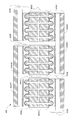
| US20120152295A1 (en) | Arrays of filled nanostructures with protruding segments and methods thereof | |
| US20120247527A1 (en) | Electrode structures for arrays of nanostructures and methods thereof | |
| KR20140012073A (ko) | 나노구조 어레이를 위한 전극 구조 및 이의 제조 방법 | |
| Hochbaum et al. | Enhanced thermoelectric performance of rough silicon nanowires | |
| US9240328B2 (en) | Arrays of long nanostructures in semiconductor materials and methods thereof | |
| KR101631042B1 (ko) | 고성능 열전 속성을 갖는 나노구조체 | |
| US9209375B2 (en) | Methods and devices for controlling thermal conductivity and thermoelectric power of semiconductor nanowires | |
| US8736011B2 (en) | Low thermal conductivity matrices with embedded nanostructures and methods thereof | |
| JP3896323B2 (ja) | 熱電冷却器およびその製造方法 | |
| US9051175B2 (en) | Bulk nano-ribbon and/or nano-porous structures for thermoelectric devices and methods for making the same | |
| CN103311262B (zh) | 微型热电器件、制作方法及包括其的温差发电机 | |
| US9082930B1 (en) | Nanostructured thermolectric elements and methods of making the same | |
| US20110168224A1 (en) | Thermoelectric device and thermoelectric device array | |
| CN103872236B (zh) | 热电薄膜结构 | |
| CN203288656U (zh) | 微型热电器件 |
Legal Events
| Date | Code | Title | Description |
|---|---|---|---|
| PA0105 | International application |
Patent event date: 20130827 Patent event code: PA01051R01D Comment text: International Patent Application |
|
| PG1501 | Laying open of application | ||
| PC1203 | Withdrawal of no request for examination | ||
| WITN | Application deemed withdrawn, e.g. because no request for examination was filed or no examination fee was paid |