KR20130122898A - Semiconductor device and manufacturing method therefor - Google Patents
Semiconductor device and manufacturing method therefor Download PDFInfo
- Publication number
- KR20130122898A KR20130122898A KR1020127023119A KR20127023119A KR20130122898A KR 20130122898 A KR20130122898 A KR 20130122898A KR 1020127023119 A KR1020127023119 A KR 1020127023119A KR 20127023119 A KR20127023119 A KR 20127023119A KR 20130122898 A KR20130122898 A KR 20130122898A
- Authority
- KR
- South Korea
- Prior art keywords
- layer
- atoms
- electrode layer
- semiconductor device
- silicon carbide
- Prior art date
Links
- 239000004065 semiconductor Substances 0.000 title claims description 38
- 238000004519 manufacturing process Methods 0.000 title claims description 18
- 125000004429 atom Chemical group 0.000 claims abstract description 80
- HBMJWWWQQXIZIP-UHFFFAOYSA-N silicon carbide Chemical compound [Si+]#[C-] HBMJWWWQQXIZIP-UHFFFAOYSA-N 0.000 claims abstract description 47
- 229910010271 silicon carbide Inorganic materials 0.000 claims abstract description 47
- 239000000758 substrate Substances 0.000 claims abstract description 44
- 125000004432 carbon atom Chemical group C* 0.000 claims abstract description 24
- 229910052710 silicon Inorganic materials 0.000 claims abstract description 22
- 229910052759 nickel Inorganic materials 0.000 claims abstract description 21
- 150000001875 compounds Chemical class 0.000 claims abstract description 8
- 239000002184 metal Substances 0.000 claims description 33
- 229910052751 metal Inorganic materials 0.000 claims description 33
- 239000000463 material Substances 0.000 claims description 29
- 238000000137 annealing Methods 0.000 claims description 17
- 238000000034 method Methods 0.000 claims description 14
- ATJFFYVFTNAWJD-UHFFFAOYSA-N Tin Chemical compound [Sn] ATJFFYVFTNAWJD-UHFFFAOYSA-N 0.000 claims description 5
- 238000010030 laminating Methods 0.000 claims description 3
- 230000001629 suppression Effects 0.000 abstract description 4
- 238000001556 precipitation Methods 0.000 abstract description 2
- 239000010410 layer Substances 0.000 description 168
- PXHVJJICTQNCMI-UHFFFAOYSA-N nickel Substances [Ni] PXHVJJICTQNCMI-UHFFFAOYSA-N 0.000 description 64
- 230000000052 comparative effect Effects 0.000 description 10
- 230000015572 biosynthetic process Effects 0.000 description 5
- 230000004048 modification Effects 0.000 description 5
- 238000012986 modification Methods 0.000 description 5
- 239000012790 adhesive layer Substances 0.000 description 3
- 238000004140 cleaning Methods 0.000 description 3
- 238000009792 diffusion process Methods 0.000 description 3
- 238000005224 laser annealing Methods 0.000 description 3
- 239000000203 mixture Substances 0.000 description 3
- 238000001004 secondary ion mass spectrometry Methods 0.000 description 3
- 238000005406 washing Methods 0.000 description 3
- CSCPPACGZOOCGX-UHFFFAOYSA-N Acetone Chemical compound CC(C)=O CSCPPACGZOOCGX-UHFFFAOYSA-N 0.000 description 2
- 229910018125 Al-Si Inorganic materials 0.000 description 2
- 229910018520 Al—Si Inorganic materials 0.000 description 2
- 229910005881 NiSi 2 Inorganic materials 0.000 description 2
- 238000000151 deposition Methods 0.000 description 2
- 230000008021 deposition Effects 0.000 description 2
- 239000012535 impurity Substances 0.000 description 2
- 238000005259 measurement Methods 0.000 description 2
- 229910021334 nickel silicide Inorganic materials 0.000 description 2
- RUFLMLWJRZAWLJ-UHFFFAOYSA-N nickel silicide Chemical compound [Ni]=[Si]=[Ni] RUFLMLWJRZAWLJ-UHFFFAOYSA-N 0.000 description 2
- 239000002244 precipitate Substances 0.000 description 2
- 238000004544 sputter deposition Methods 0.000 description 2
- -1 that is Inorganic materials 0.000 description 2
- OKTJSMMVPCPJKN-UHFFFAOYSA-N Carbon Chemical compound [C] OKTJSMMVPCPJKN-UHFFFAOYSA-N 0.000 description 1
- 238000010521 absorption reaction Methods 0.000 description 1
- 239000000654 additive Substances 0.000 description 1
- 239000000356 contaminant Substances 0.000 description 1
- 230000000694 effects Effects 0.000 description 1
- 238000000921 elemental analysis Methods 0.000 description 1
- 238000005530 etching Methods 0.000 description 1
- 230000005669 field effect Effects 0.000 description 1
- 229910002804 graphite Inorganic materials 0.000 description 1
- 239000010439 graphite Substances 0.000 description 1
- 229910044991 metal oxide Inorganic materials 0.000 description 1
- 150000004706 metal oxides Chemical class 0.000 description 1
- 229910003465 moissanite Inorganic materials 0.000 description 1
- 239000003960 organic solvent Substances 0.000 description 1
- 238000005498 polishing Methods 0.000 description 1
- 238000002360 preparation method Methods 0.000 description 1
- 229910021484 silicon-nickel alloy Inorganic materials 0.000 description 1
Images


Classifications
-
- H—ELECTRICITY
- H01—ELECTRIC ELEMENTS
- H01L—SEMICONDUCTOR DEVICES NOT COVERED BY CLASS H10
- H01L29/00—Semiconductor devices adapted for rectifying, amplifying, oscillating or switching, or capacitors or resistors with at least one potential-jump barrier or surface barrier, e.g. PN junction depletion layer or carrier concentration layer; Details of semiconductor bodies or of electrodes thereof ; Multistep manufacturing processes therefor
- H01L29/66—Types of semiconductor device ; Multistep manufacturing processes therefor
- H01L29/68—Types of semiconductor device ; Multistep manufacturing processes therefor controllable by only the electric current supplied, or only the electric potential applied, to an electrode which does not carry the current to be rectified, amplified or switched
- H01L29/76—Unipolar devices, e.g. field effect transistors
- H01L29/772—Field effect transistors
- H01L29/78—Field effect transistors with field effect produced by an insulated gate
- H01L29/7801—DMOS transistors, i.e. MISFETs with a channel accommodating body or base region adjoining a drain drift region
- H01L29/7802—Vertical DMOS transistors, i.e. VDMOS transistors
-
- H—ELECTRICITY
- H01—ELECTRIC ELEMENTS
- H01L—SEMICONDUCTOR DEVICES NOT COVERED BY CLASS H10
- H01L21/00—Processes or apparatus adapted for the manufacture or treatment of semiconductor or solid state devices or of parts thereof
- H01L21/02—Manufacture or treatment of semiconductor devices or of parts thereof
- H01L21/04—Manufacture or treatment of semiconductor devices or of parts thereof the devices having at least one potential-jump barrier or surface barrier, e.g. PN junction, depletion layer or carrier concentration layer
- H01L21/18—Manufacture or treatment of semiconductor devices or of parts thereof the devices having at least one potential-jump barrier or surface barrier, e.g. PN junction, depletion layer or carrier concentration layer the devices having semiconductor bodies comprising elements of Group IV of the Periodic System or AIIIBV compounds with or without impurities, e.g. doping materials
- H01L21/28—Manufacture of electrodes on semiconductor bodies using processes or apparatus not provided for in groups H01L21/20 - H01L21/268
-
- H—ELECTRICITY
- H01—ELECTRIC ELEMENTS
- H01L—SEMICONDUCTOR DEVICES NOT COVERED BY CLASS H10
- H01L21/00—Processes or apparatus adapted for the manufacture or treatment of semiconductor or solid state devices or of parts thereof
- H01L21/02—Manufacture or treatment of semiconductor devices or of parts thereof
- H01L21/04—Manufacture or treatment of semiconductor devices or of parts thereof the devices having at least one potential-jump barrier or surface barrier, e.g. PN junction, depletion layer or carrier concentration layer
- H01L21/0445—Manufacture or treatment of semiconductor devices or of parts thereof the devices having at least one potential-jump barrier or surface barrier, e.g. PN junction, depletion layer or carrier concentration layer the devices having semiconductor bodies comprising crystalline silicon carbide
- H01L21/048—Making electrodes
- H01L21/0485—Ohmic electrodes
-
- H—ELECTRICITY
- H01—ELECTRIC ELEMENTS
- H01L—SEMICONDUCTOR DEVICES NOT COVERED BY CLASS H10
- H01L21/00—Processes or apparatus adapted for the manufacture or treatment of semiconductor or solid state devices or of parts thereof
- H01L21/02—Manufacture or treatment of semiconductor devices or of parts thereof
- H01L21/04—Manufacture or treatment of semiconductor devices or of parts thereof the devices having at least one potential-jump barrier or surface barrier, e.g. PN junction, depletion layer or carrier concentration layer
- H01L21/18—Manufacture or treatment of semiconductor devices or of parts thereof the devices having at least one potential-jump barrier or surface barrier, e.g. PN junction, depletion layer or carrier concentration layer the devices having semiconductor bodies comprising elements of Group IV of the Periodic System or AIIIBV compounds with or without impurities, e.g. doping materials
- H01L21/26—Bombardment with radiation
- H01L21/263—Bombardment with radiation with high-energy radiation
- H01L21/268—Bombardment with radiation with high-energy radiation using electromagnetic radiation, e.g. laser radiation
-
- H—ELECTRICITY
- H01—ELECTRIC ELEMENTS
- H01L—SEMICONDUCTOR DEVICES NOT COVERED BY CLASS H10
- H01L29/00—Semiconductor devices adapted for rectifying, amplifying, oscillating or switching, or capacitors or resistors with at least one potential-jump barrier or surface barrier, e.g. PN junction depletion layer or carrier concentration layer; Details of semiconductor bodies or of electrodes thereof ; Multistep manufacturing processes therefor
- H01L29/02—Semiconductor bodies ; Multistep manufacturing processes therefor
- H01L29/12—Semiconductor bodies ; Multistep manufacturing processes therefor characterised by the materials of which they are formed
-
- H—ELECTRICITY
- H01—ELECTRIC ELEMENTS
- H01L—SEMICONDUCTOR DEVICES NOT COVERED BY CLASS H10
- H01L29/00—Semiconductor devices adapted for rectifying, amplifying, oscillating or switching, or capacitors or resistors with at least one potential-jump barrier or surface barrier, e.g. PN junction depletion layer or carrier concentration layer; Details of semiconductor bodies or of electrodes thereof ; Multistep manufacturing processes therefor
- H01L29/40—Electrodes ; Multistep manufacturing processes therefor
- H01L29/43—Electrodes ; Multistep manufacturing processes therefor characterised by the materials of which they are formed
- H01L29/45—Ohmic electrodes
-
- H—ELECTRICITY
- H01—ELECTRIC ELEMENTS
- H01L—SEMICONDUCTOR DEVICES NOT COVERED BY CLASS H10
- H01L29/00—Semiconductor devices adapted for rectifying, amplifying, oscillating or switching, or capacitors or resistors with at least one potential-jump barrier or surface barrier, e.g. PN junction depletion layer or carrier concentration layer; Details of semiconductor bodies or of electrodes thereof ; Multistep manufacturing processes therefor
- H01L29/66—Types of semiconductor device ; Multistep manufacturing processes therefor
- H01L29/66007—Multistep manufacturing processes
- H01L29/66053—Multistep manufacturing processes of devices having a semiconductor body comprising crystalline silicon carbide
- H01L29/66068—Multistep manufacturing processes of devices having a semiconductor body comprising crystalline silicon carbide the devices being controllable only by the electric current supplied or the electric potential applied, to an electrode which does not carry the current to be rectified, amplified or switched, e.g. three-terminal devices
-
- H—ELECTRICITY
- H01—ELECTRIC ELEMENTS
- H01L—SEMICONDUCTOR DEVICES NOT COVERED BY CLASS H10
- H01L29/00—Semiconductor devices adapted for rectifying, amplifying, oscillating or switching, or capacitors or resistors with at least one potential-jump barrier or surface barrier, e.g. PN junction depletion layer or carrier concentration layer; Details of semiconductor bodies or of electrodes thereof ; Multistep manufacturing processes therefor
- H01L29/02—Semiconductor bodies ; Multistep manufacturing processes therefor
- H01L29/12—Semiconductor bodies ; Multistep manufacturing processes therefor characterised by the materials of which they are formed
- H01L29/16—Semiconductor bodies ; Multistep manufacturing processes therefor characterised by the materials of which they are formed including, apart from doping materials or other impurities, only elements of Group IV of the Periodic System
- H01L29/1608—Silicon carbide
Abstract
전극층(16)은, 탄화규소 기판(90) 위에 접하고, Ni 원자 및 Si 원자를 갖는다. Ni 원자의 수는 Ni 원자 및 Si 원자의 총 수의 67% 이상이다. 전극층(16)의 적어도 탄화규소 기판(90)에 접하는 측은 Si 및 Ni의 화합물을 포함한다. 전극층(16)의 표면측에서 C 원자 농도는 Ni 원자 농도보다 작다. 이에 의해, 전극층(16)의 전기 전도도의 향상과, 전극층(16)의 표면에의 C 원자의 석출의 억제를 양립시킬 수 있다.The electrode layer 16 is in contact with the silicon carbide substrate 90 and has Ni atoms and Si atoms. The number of Ni atoms is at least 67% of the total number of Ni atoms and Si atoms. At least the side of the electrode layer 16 in contact with the silicon carbide substrate 90 contains a compound of Si and Ni. The C atom concentration at the surface side of the electrode layer 16 is smaller than the Ni atom concentration. Thereby, the improvement of the electrical conductivity of the electrode layer 16 and the suppression of the precipitation of C atoms to the surface of the electrode layer 16 can be made compatible.
Description
본 발명은, 반도체 장치 및 그 제조 방법에 관한 것이며, 보다 특정적으로는, 탄화규소 기판을 갖는 반도체 장치 및 그 제조 방법에 관한 것이다. TECHNICAL FIELD This invention relates to a semiconductor device and its manufacturing method. More specifically, It is related with the semiconductor device which has a silicon carbide substrate, and its manufacturing method.
탄화규소 기판을 이용한 반도체 장치의 제조 방법에서, 탄화규소 기판 위에 오믹 전극을 형성하는 기술의 개발이 행해지고 있다. In the manufacturing method of the semiconductor device using a silicon carbide substrate, development of the technique which forms an ohmic electrode on a silicon carbide substrate is performed.
예컨대 일본 특허 공개 평성07-99169호 공보(특허문헌 1)에 의하면, SiC 기체(탄화규소 기판) 위에 Ni-Si 합금층, 또는 Si, Ni 적층체를 형성해 두면, SiC 기체로부터의 Si의 공급없이 NiSi2(Ni 33 원자%, Si 67 원자%)을 형성할 수 있고, SiC 기체에 대하여 오믹 접촉을 하는 전극이 얻어지는 것으로 되어 있다. 또한 이 공보에 의하면, Ni이 원자비로 33% 이하에서는 Si가 잉여가 되어 전도성을 저해하고, 67% 이상이면 NiSi2와 SiC의 계면에 잉여 Ni가 존재하여, 불연속적인 계면이 되어 버리는 것으로 되어 있다. 또한 이 공보에 의하면, Si를 SiC로부터 공급하는 것이 아니기 때문에 잉여가 된 C가 Ni내에 확산되어 전극 표면에 그래파이트로서 석출되는 현상도 생기지 않는 것으로 되어 있다.For example, according to Japanese Patent Application Laid-Open No. 07-99169 (Patent Document 1), if a Ni-Si alloy layer, or a Si or Ni laminate is formed on a SiC substrate (silicon carbide substrate), without supply of Si from the SiC substrate, NiSi 2 (Ni 33 at.%, 67 at% Si) can be formed, it is that the electrode for ohmic contact with the SiC substrate obtained. According to this publication, when Ni is 33% or less in terms of atomic ratio, Si becomes excess and inhibits conductivity. When 67% or more, excess Ni is present at the interface between NiSi 2 and SiC, resulting in a discontinuous interface. have. According to this publication, since Si is not supplied from SiC, the phenomenon that excess C diffuses into Ni and precipitates as graphite on the electrode surface does not occur.
전술한 바와 같이, Ni 원자 및 Si 원자를 갖는 전극(전극층)의 형성에 있어서, 전극층의 전기 전도도를 높게 하기 위해서는, Ni의 비율을 높여야 한다. 그러나 Ni의 비율이 높아지면, 전극층 형성을 위한 어닐링시에, 탄화규소 기판으로부터 전극층의 표면에 많은 C 원자가 석출되어 버린다. 이 때문에 전극층의 전기 전도도를 높게 하는 것과, 전극층의 표면에의 C 원자의 석출의 억제를 양립시키기 어려웠다. As described above, in forming the electrode (electrode layer) having Ni atoms and Si atoms, the ratio of Ni must be increased in order to increase the electrical conductivity of the electrode layer. However, when the ratio of Ni increases, many C atoms will precipitate from the silicon carbide substrate on the surface of the electrode layer at the time of annealing for forming the electrode layer. For this reason, it was difficult to make both the electrical conductivity of an electrode layer high and suppression of the precipitation of C atoms to the surface of an electrode layer.
이 때문에 본 발명의 목적은, 전극층의 전기 전도도의 향상과, 전극층의 표면에의 C 원자의 석출의 억제를 양립시킬 수 있는 반도체 장치 및 그 제조 방법을 제공하는 것이다. For this reason, it is an object of the present invention to provide a semiconductor device capable of achieving both an improvement in the electrical conductivity of the electrode layer and suppression of the deposition of C atoms on the surface of the electrode layer, and a method of manufacturing the same.
본 발명의 반도체 장치는 탄화규소 기판 및 전극층을 갖는다. 전극층은, 탄화규소 기판 위에 접하고, Ni 원자 및 Si 원자를 갖는다. Ni 원자의 수는 Ni 원자 및 Si 원자의 총 수의 67% 이상이다. 전극층의 적어도 탄화규소 기판에 접하는 측은 Si 및 Ni의 화합물을 포함한다. 전극층의 표면측에서 C 원자 농도는 Ni 원자 농도보다 작다. The semiconductor device of the present invention has a silicon carbide substrate and an electrode layer. The electrode layer is in contact with the silicon carbide substrate and has Ni atoms and Si atoms. The number of Ni atoms is at least 67% of the total number of Ni atoms and Si atoms. At least the side of the electrode layer in contact with the silicon carbide substrate contains a compound of Si and Ni. The C atom concentration at the surface side of the electrode layer is smaller than the Ni atom concentration.
이 반도체 장치에 의하면, 전극층에서 Ni 원자의 수는 Ni 원자 및 Si 원자의 총 수의 67% 이상이다. 이에 의해 이 퍼센테이지가 67% 미만인 경우에 비해 전극층의 전기 전도도를 높일 수 있다. 또한 이 반도체 장치에 의하면, 전극층의 표면측에서 C 원자 농도는 Ni 원자 농도보다 작다. 이에 의해, 전극층의 표면측에 접하는 금속 패드층이 형성된 경우에, 이 금속 패드층을 박리하기 어려워진다.According to this semiconductor device, the number of Ni atoms in the electrode layer is 67% or more of the total number of Ni atoms and Si atoms. Thereby, compared with the case where this percentage is less than 67%, the electrical conductivity of an electrode layer can be improved. According to this semiconductor device, the C atom concentration on the surface side of the electrode layer is smaller than the Ni atom concentration. Thereby, when the metal pad layer which contacts the surface side of an electrode layer is formed, it will become difficult to peel this metal pad layer.
바람직하게는 전극층의 표면측에서, C 원자 농도는 3% 미만이다. Preferably, at the surface side of the electrode layer, the C atom concentration is less than 3%.
바람직하게는 반도체 장치는, 전극층의 표면측에 접하는 금속 패드층을 갖는다. 금속 패드층은 바람직하게는 Al층이다. 바람직하게는 금속 패드층은, 전극층 위에 형성된 밀착층과, 밀착층 위에 형성된 본체층을 포함한다. 밀착층은 Ti, TiW, 및 TiN 중 어느 하나로 만들어져 있다. Preferably, the semiconductor device has a metal pad layer in contact with the surface side of the electrode layer. The metal pad layer is preferably an Al layer. Preferably, the metal pad layer includes an adhesion layer formed on the electrode layer and a body layer formed on the adhesion layer. The adhesive layer is made of any one of Ti, TiW, and TiN.
바람직하게는 전극층의 표면측에서의 Si 원자 농도는 30%보다 작다. 이에 의해 전극층의 전기 전도도를 보다 높일 수 있다. Preferably, the Si atom concentration at the surface side of the electrode layer is less than 30%. Thereby, the electrical conductivity of an electrode layer can be raised more.
본 발명의 반도체 장치의 제조 방법은, 이하의 공정을 갖는다. 탄화규소 기판이 준비된다. 탄화규소 기판 위에 접하고, Ni 원자 및 Si 원자를 갖는 재료층이 형성된다. Ni 원자의 수는 Ni 원자 및 Si 원자의 총 수의 67% 이상이다. 재료층을 레이저광으로 어닐링하는 것에 의해, 적어도 탄화규소 기판에 접하는 측에 Si 및 Ni의 화합물을 포함하는 전극층이 형성된다.The manufacturing method of the semiconductor device of this invention has the following processes. A silicon carbide substrate is prepared. In contact with the silicon carbide substrate, a material layer having Ni atoms and Si atoms is formed. The number of Ni atoms is at least 67% of the total number of Ni atoms and Si atoms. By annealing the material layer with a laser beam, an electrode layer containing a compound of Si and Ni is formed at least on the side in contact with the silicon carbide substrate.
이 반도체 장치의 제조 방법에 의하면, 전극층의 재료가 되는 재료층에서, Ni 원자의 수는 Ni 원자 및 Si 원자의 총 수의 67% 이상이다. 이에 의해 퍼센테이지가 67% 미만인 경우에 비해 전극층의 전기 전도도를 높일 수 있다. 또한 이 반도체 장치의 제조 방법에 의하면, 레이저광이 이용되는 것에 의해 어닐링이 단시간에 행해진다. 이에 의해, 보다 장시간에 걸친 어닐링이 행해진 경우에 비해, C 원자의 확산을 억제할 수 있다. 따라서 전극층의 표면측에서의 C 원자 농도를 낮게 할 수 있다. 이에 의해, 전극층의 표면측에 접하는 금속 패드층이 형성된 경우에 이 금속 패드층을 박리하기 어려워진다.According to this semiconductor device manufacturing method, in the material layer serving as the material of the electrode layer, the number of Ni atoms is 67% or more of the total number of Ni atoms and Si atoms. Thereby, the electrical conductivity of an electrode layer can be improved compared with the case where the percentage is less than 67%. Moreover, according to the manufacturing method of this semiconductor device, annealing is performed in a short time by using a laser beam. Thereby, diffusion of C atoms can be suppressed compared with the case where annealing for a longer time is performed. Therefore, C atom concentration in the surface side of an electrode layer can be made low. Thereby, when the metal pad layer which contacts the surface side of an electrode layer is formed, it will become difficult to peel this metal pad layer.
바람직하게는, 전극층 위에 금속 패드층이 형성된다. 금속 패드층은 바람직하게는 Al층을 포함한다. 바람직하게는 금속 패드층을 형성하는 공정은, 전극층 위에 밀착층을 형성하는 공정과, 밀착층 위에 본체층을 형성하는 공정을 포함한다. 밀착층은 Ti, TiW, 및 TiN 중 어느 하나로 형성된다. Preferably, a metal pad layer is formed on the electrode layer. The metal pad layer preferably comprises an Al layer. Preferably, the process of forming a metal pad layer includes the process of forming an adhesion layer on an electrode layer, and the process of forming a main body layer on an adhesion layer. The adhesive layer is formed of any one of Ti, TiW, and TiN.
재료층을 형성하는 공정은, Si 및 Ni의 혼합층을 형성하는 공정을 포함하여도 좋다. 또한 재료층을 형성하는 공정은, Si층 및 Ni층을 적층하는 공정을 포함하여도 좋다. The step of forming the material layer may include a step of forming a mixed layer of Si and Ni. In addition, the step of forming the material layer may include a step of laminating the Si layer and the Ni layer.
전술한 바와 같이 본 발명에 의하면, 전극층의 전기 전도도를 높이는 것과, 전극층의 표면에의 C 원자의 석출의 억제를 양립시킬 수 있다. As described above, according to the present invention, both the electrical conductivity of the electrode layer and the suppression of the deposition of C atoms on the surface of the electrode layer can be made compatible.
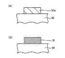
도 1은 본 발명의 제1 실시형태에서의 반도체 장치의 구성을 개략적으로 도시하는 단면도이다.
도 2는 도 1의 반도체 장치의 제조 방법의 제1 공정(A) 및 제2 공정(B)을 개략적으로 도시하는 단면도이다.
도 3은 도 1의 반도체 장치의 변형예를 개략적으로 도시하는 단면도이다.
도 4는 본 발명의 제2 실시형태에서의 반도체 장치의 제조 방법의 일 공정을 개략적으로 도시하는 단면도이다.
도 5는 본 발명의 제3 실시형태에서의 반도체 장치의 구성을 개략적으로 도시하는 단면도이다.
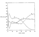
도 6은 제1 비교예의 반도체 장치의 원자 농도 프로파일이다.
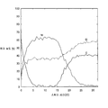
도 7은 제2 비교예의 반도체 장치의 원자 농도 프로파일이다.
도 8은 제3 비교예의 반도체 장치의 원자 농도 프로파일이다. 1 is a cross-sectional view schematically showing the configuration of a semiconductor device according to a first embodiment of the present invention.
FIG. 2: is sectional drawing which shows schematically the 1st process A and 2nd process (B) of the manufacturing method of the semiconductor device of FIG.
3 is a cross-sectional view schematically showing a modification of the semiconductor device of FIG. 1.
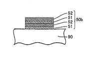
It is sectional drawing which shows schematically one process of the manufacturing method of the semiconductor device in 2nd Embodiment of this invention.
5 is a cross-sectional view schematically showing the configuration of a semiconductor device according to a third embodiment of the present invention.
6 is an atomic concentration profile of the semiconductor device of the first comparative example.
7 is an atomic concentration profile of the semiconductor device of the second comparative example.
8 is an atomic concentration profile of the semiconductor device of the third comparative example.
이하, 본 발명의 실시형태에 대해서 도면에 기초하여 설명한다. DESCRIPTION OF THE PREFERRED EMBODIMENTS Hereinafter, embodiments of the present invention will be described with reference to the drawings.
(제1 실시형태)(First embodiment)
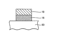
도 1을 참조하면, 본 실시형태의 반도체 장치는, 탄화규소 기판(90)과, 전극층(16)과, 금속 패드층(19)을 갖는다. Referring to FIG. 1, the semiconductor device of this embodiment includes a
전극층(16)은, 탄화규소 기판(90) 위에 접하고, Ni 원자 및 Si 원자를 갖는다. Ni 원자의 수는 Ni 원자 및 Si 원자의 총 수의 67% 이상이다. 보다 구체적으로는, 전극층(16) 재료의 개략적인 조성은, 67 원자% 이상의 Ni과, 그 실질적인 잔부인 Si와의 혼합물이다. 단 필요에 따라 전극층(16) 재료에 Ni 및 Si 이외의 첨가물이 가해져도 좋다. 또한 전극층(16)의 재료는, 공업적인 제조 방법에서 불가피하게 수반되는 불순물을 포함할 수 있다.The
바람직하게는, 전극층(16)에서의 Si 원자의 수는, Ni 원자 및 Si 원자의 총 수의 10% 이상이다. Preferably, the number of Si atoms in the
전극층(16)의 적어도 탄화규소 기판(90)에 접하는 측은 Si 및 Ni의 화합물, 즉 니켈실리사이드를 포함한다. 이에 의해 전극층(16)과 탄화규소 기판(90)은 오믹 접속되어 있다. 즉 전극층(16)은 오믹 전극으로서의 기능을 갖는다. At least the side of the
전극층(16)의 탄화규소 기판(90)에 접하는 측(도면중, 하측)에서는, 전술한 화합물은 대략 Ni2Si 이다. 즉, 전극층(16)의 탄화규소 기판(90)에 접하는 측에서는, Ni 및 Si의 총원자수에 대한 Ni 원자수의 비율은, 대략 3분의 2 즉, 대략 67% 이다. 이 비율은, 전극층(16)의 표면측(도면중, 상측)에서 보다 높아져 있고, 극단적인 경우 100%에 가까운 값이어도 좋다. 즉, 공업적인 제조 방법에서의 불가피한 불순물, 또는 외부 환경으로부터의 불가피한 부착물을 별개로 하면, 전극층(16)의 표면측이 실질적으로 Ni로 구성되어 있어도 좋다. 이 경우, 전극층(16)의 표면측의 전기 전도도는, Si를 유의(有意)로 포함하는 경우에 비해, 보다 높아진다. The side in contact with the
전극층(16)의 표면측에서, C 원자 농도는 Ni 원자 농도보다 작다. 바람직하게는 이 C 원자 농도는 3% 미만이며, 보다 바람직하게는 1% 미만이다. 보다 바람직하게는, 전극층(16)의 표면측에 실질적으로 C 원자가 존재하지 않는다. 즉 외부 환경으로부터의 불가피한 C 원자의 부착을 별개로 하면, 전극층(16)의 표면측이 실질적으로 Ni로 구성되어 있더라도 좋다. At the surface side of the
여기서 표면측에서의 원자 농도란, 전극층(16)의 표면(도면 중 상부면)으로부터 깊이 5 ㎚까지의 영역에서의 전체 원자수에 대한 특정 원자의 수의 비율이다. 이 원자 농도는, 깊이 방향의 분해능이 높은 원소 분석에 의해 측정할 수 있고, 예컨대 SIMS(Secondary Ion Mass Spectroscopy)에 의해 측정할 수 있다. 또한 측정 준비 작업에서 전극층(16)의 표면이 대기에 노출되어 있던 경우는, 전극층(16)의 표면을 세정해야 한다. 이 세정은, 예컨대 아세톤 등의 유기 용제를 이용한 초음파 세정이다. Here, the atomic concentration on the surface side is the ratio of the number of specific atoms to the total number of atoms in the region from the surface (upper surface in the drawing) of the
바람직하게는, 전극층(16) 자체의 표면은, 에칭 또는 연마 등에 의한 물질 제거가 행해져 있지 않은 면이다. 이에 의해 전극층(16)의 형성 공정이 보다 간편화되어 있다. 단 이 경우라도, 전극층(16)의 형성 후에 외부 환경으로부터 전극층(16)의 표면에 부착된 오염 물질은 제거되어 있어도 좋다. 이 제거는, 예컨대 전술한 바와 같은 세정에 의해 행해질 수 있다.Preferably, the surface of the
금속 패드층(19)은 전극층(16)의 표면측에 접해 있다. 금속 패드층(19)은 바람직하게는 Al층 또는 Al-Si층이다. The
다음으로 본 실시형태의 반도체 장치의 제조 방법에 대해서 설명한다. Next, the manufacturing method of the semiconductor device of this embodiment is demonstrated.
도 2의 (A)를 참조하면, 우선 탄화규소 기판(90)이 준비된다. 다음으로, 탄화규소 기판(90) 위에 접하고, Ni 원자 및 Si 원자를 갖는 재료층(50a)이 형성된다. Ni 원자의 수는 Ni 원자 및 Si 원자의 총 수의 67% 이상이다. 재료층(50a)은, Si 및 Ni의 혼합층이다. 이 혼합층의 형성은, 예컨대 Si로 이루어지는 타겟과, Ni로 이루어지는 타겟을 동시에 스퍼터하는 것에 의해 행할 수 있다. Referring to FIG. 2A, first, a
바람직하게는, 재료층(50a)에서의 Si 원자의 수는, Ni 원자 및 Si 원자의 총 수의 10% 이상이다. Preferably, the number of Si atoms in the
도 2의 (B)를 더 참조하면, 어닐링 처리로서, 재료층(50a)[도 2의 (A)]이 형성된 탄화규소 기판(90) 위에 레이저광이 조사된다. 이 어닐링에 의해 재료층(50a)으로부터 전극층(16)[도 2의 (B)]이 형성된다. 이 어닐링은, 전극층(16)의 적어도 탄화규소 기판(90)에 접하는 측이 Si 및 Ni의 화합물 즉 니켈실리사이드를 포함하는 것으로 되도록 행해진다. Referring to Fig. 2B further, as an annealing treatment, laser light is irradiated onto the
바람직하게는 레이저광의 파장은, 탄화규소의 밴드갭에 대응하는 파장인 386 ㎚ 이하이다. 이에 의해 탄화규소 기판(90)의 표면에서 레이저광의 흡수가 생긴다. 이러한 레이저광으로서는, 예컨대 YAG 레이저 또는 YVO4 레이저의 제3 고조파인 파장 355 ㎚의 광을 이용할 수 있다. Preferably, the wavelength of a laser beam is 386 nm or less which is a wavelength corresponding to the band gap of silicon carbide. As a result, absorption of the laser light occurs on the surface of the
또한 레이저광의 출력 밀도는, 0.5 J/㎠ 이상 1.5 J/㎠ 이하이며, 보다 바람직하게는, 0.7 J/㎠ 이상 1.3 J/㎠ 이하이다. 이에 의해, 충분한 어닐링의 작용을 얻고, 레이저광에 의한 손상의 발생을 억제할 수 있다. Moreover, the output density of a laser beam is 0.5 J / cm <2> or more and 1.5 J / cm <2>, More preferably, they are 0.7 J / cm <2> or more and 1.3 J / cm <2> or less. Thereby, sufficient annealing action can be obtained and generation | occurrence | production of the damage by a laser beam can be suppressed.
또한 레이저광의 펄스폭은, 10 ㎱ 이상 10 ㎲ 이하가 되고, 보다 바람직하게는 50 ㎱ 이상 1 ㎲ 이하가 된다. 이에 의해, 실용적인 펄스폭을 갖는 레이저를 이용하면서, 충분히 짧은 시간으로 어닐링을 행할 수 있다. Moreover, the pulse width of a laser beam becomes 10 kW or more and 10 kW or less, More preferably, it is 50 kW or more and 1 kW or less. Thereby, annealing can be performed in sufficiently short time, using the laser which has a practical pulse width.
다시 도 1을 참조하면, 전극층(16) 위에 금속 패드층(19)이 형성된다. 금속 패드층(19)은 바람직하게는 Al층이다. 이상에 의해 본 실시형태의 반도체 장치가 얻어진다. Referring back to FIG. 1, a
본 실시형태의 반도체 장치에 의하면, 전극층(16)에서 Ni 원자의 수는 Ni 원자 및 Si 원자의 총 수의 67% 이상이다. 이에 의해 이 퍼센테이지가 67% 미만인 경우에 비해 전극층(16)의 전기 전도도를 높일 수 있다. 또한 이 반도체 장치에 의하면, 전극층(16)의 표면측은 Si 원자 농도 및 Ni 원자 농도의 합보다 작은 C 원자 농도를 갖는다. 이에 의해, 전극층(16)의 표면측에 접하는 금속 패드층(19)이 형성된 경우에 이 금속 패드층(19)을 박리하기 어려워진다.According to the semiconductor device of this embodiment, the number of Ni atoms in the
바람직하게는 전극층(16)의 표면측에서의 Si 원자 농도는 30%보다 작다. 이에 의해 전극층(16)의 전기 전도도를 보다 높일 수 있다. Preferably, the Si atom concentration at the surface side of the
또한 본 실시형태의 반도체 장치의 제조 방법에 의하면, 전극층(16)의 재료가 되는 재료층(50a)에서, Ni 원자의 수는 Ni 원자 및 Si 원자의 총 수의 67% 이상이다. 이에 의해 이 퍼센테이지가 67% 미만인 경우에 비해 전극층(16)의 전기 전도도를 높일 수 있다. Moreover, according to the manufacturing method of the semiconductor device of this embodiment, in the
또한 레이저광이 이용되는 것에 의해 어닐링이 단시간에 행해진다. 이에 의해, 예컨대 램프 어닐링과 같이, 보다 장시간에 걸친 어닐링이 행해진 경우에 비해, C 원자의 확산을 억제할 수 있다. 따라서 전극층(16)의 표면측에서의 C 원자 농도를 낮게 할 수 있다. 이에 의해, 전극층(16)의 표면측에 접하는 금속 패드층(19)이 형성된 경우에 금속 패드층(19)을 박리하기 어려워진다.In addition, annealing is performed in a short time by using a laser beam. Thereby, diffusion of C atoms can be suppressed compared with the case where annealing for a longer time is performed like a lamp annealing, for example. Therefore, C atom concentration in the surface side of the
바람직하게는, 전극층(16) 또는 재료층(50a)의 Ni 원자의 수는 Ni 원자 및 Si 원자의 총 수의 70% 이상이다. 이에 의해 전술한 작용 효과를 보다 확실하게 얻을 수 있다. 또한 바람직하게는 Ni 원자의 수는 Ni 원자 및 Si 원자의 총 수의 90% 이하이다. 이에 의해 탄화규소 기판(90)으로부터의 C 원자의 확산을 보다 억제할 수 있다. Preferably, the number of Ni atoms in the
다음으로 본 실시형태의 변형예에 대해서 설명한다. Next, the modification of this embodiment is demonstrated.
도 3을 참조하면, 본 변형예의 반도체 장치의 금속 패드층(19V)은, 전극층(16) 위에 형성된 밀착층(19a)과, 밀착층(19a) 위에 형성된 본체층(19b)을 포함한다. 밀착층(19a)은 Ti, TiW, 및 TiN 중 어느 하나로 만들어져 있다. 본체층(19b)은, 바람직하게는 Al층 또는 Al-Si층이다. Referring to FIG. 3, the
본 변형예에 의하면, 금속 패드층(19V)의 전극층(16)에의 밀착성을 보다 높일 수 있다. According to this modification, the adhesiveness of the
(제2 실시형태)(Second Embodiment)
주로 도 4를 참조하면, 본 실시형태에서는 재료층(50a)[도 2의 (A)] 대신에 재료층(50b)이 형성된다. 재료층(50b)을 형성하는 공정은 Si층(51) 및 Ni층(52)을 적층하는 공정을 포함한다. 바람직하게는, 형성되는 적층체의 최상층은 Ni층(52)이 된다. 이에 의해, 어닐링 후에 얻어지는 전극층(16)의 표면측에서의 Ni 원자의 비율을 높일 수 있기 때문에, 전극층(16)의 표면측의 전기 전도도를 높일 수 있다. Mainly referring to FIG. 4, in this embodiment, the
또한, 상기 이외의 구성에 대해서는, 전술한 제1 실시형태의 구성과 거의 동일하기 때문에, 동일 또는 대응하는 요소에 대해서 동일한 부호를 붙이고, 그 설명을 반복하지 않는다. In addition, about the structure of that excepting the above, since it is substantially the same as the structure of 1st Embodiment mentioned above, the same code | symbol is attached | subjected about the same or corresponding element, and the description is not repeated.
본 실시형태에 의하면, 제1 실시형태에서 행해진 바와 같은 Ni 및 Si의 혼합층의 형성이 불필요해진다. According to this embodiment, formation of the mixed layer of Ni and Si as performed in 1st Embodiment becomes unnecessary.
(제3 실시형태)(Third Embodiment)
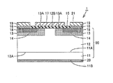
본 실시형태에서는, 전술한 제1 실시형태 또는 제2 실시형태의 반도체 장치의 보다 상세한 구조의 일례에 대해서 설명한다.In this embodiment, an example of a more detailed structure of the semiconductor device of the first embodiment or the second embodiment described above will be described.
도 5를 참조하면, 본 실시형태의 반도체 장치는, 종형 MOSFET(Metal Oxide Semiconductor Field Effect Tra㎱istor)이며, 탄화규소 기판(90)과, 전극층(16)과, 금속 패드층(19)과, 게이트 절연막(15)과, 게이트 전극(17)을 갖는다. 탄화규소 기판(90)은, n+층(11), n-층(12), p 보디층(13), n+ 소스 영역(14), p+ 영역(18)을 갖는다. Referring to FIG. 5, the semiconductor device of the present embodiment is a vertical MOSFET (Metal Oxide Semiconductor Field Effect Traistor), and includes a
전극층(16)은, 탄화규소 기판(90)의 한쪽 면(도면중 상부면) 위에서, n+ 소스 영역(14) 및 p+ 영역(18) 각각에 오믹 접합되도록 설치되어 있다. 전극층(16)의 두께는, 예컨대 100 ㎚∼200 ㎚ 정도이다. The
게이트 전극(17)은, 탄화규소 기판(90)의 한쪽 면(도면중의 상부면) 위에 게이트 절연막(15)을 개재하여 설치되어 있고, p 보디층(13)의 표면측인 채널 영역(13A)에 대향되어 있다. 또한 탄화규소 기판(90)의 다른쪽 면(도면중 하부면) 위에는 드레인 전극(20)이 설치되어 있다. The
본 실시형태에 의하면, 전기 전도도가 높은 전극층(16)과, 박리하기 어려운 금속 패드층(19)을 갖는 종형 MOSFET가 얻어진다. According to this embodiment, the vertical MOSFET which has the
또한 탄화규소 기판(90)의 드레인 전극(20)에 면하는 측에 p 콜렉터층이 형성되는 것에 의해, 종형 MOSFET 대신에 종형 IGBT(I㎱ulated Gate Bipolar Tra㎱istor)가 구성되어도 좋다. 또한 탄화규소 기판에 형성된 트렌치내에 게이트 절연막을 개재하여 게이트 전극이 매립되는 구조(트렌치 게이트 구조)가 이용되어도 좋다. Further, by forming the p collector layer on the side of the
(비교예)(Comparative Example)
SIMS를 이용한 농도 프로파일 데이터를 참조하면서, 본 발명에 대한 비교예에 대해서 설명한다. 또한 금속층의 표면 위에의 금속 패드층의 형성은 행해지 않았기 때문에, 농도 프로파일에서의 스퍼터 시간 0 근방이 전극층의 표면에 대응한다. 또한 스퍼터 레이트는 약 10 ㎚/분으로 되어 있다. 또한 측정 전에는, 표면의 세정 처리가 행해졌다. 이하에, 비교예에 대해서 구체적으로 설명한다. The comparative example with respect to this invention is demonstrated, referring the density profile data using SIMS. In addition, since the formation of the metal pad layer on the surface of the metal layer was not performed, the vicinity of the sputtering time zero in the concentration profile corresponds to the surface of the electrode layer. In addition, the sputter rate is about 10 nm / minute. In addition, the surface cleaning process was performed before measurement. Below, a comparative example is explained concretely.
(제1 비교예)(Comparative Example 1)
재료층(50a) 대신에 Ni층이 이용되었다. 또한 레이저 어닐링 대신에 램프 어닐링이 이용되었다. Instead of the
도 6을 참조하면, 전극층의 표면(그래프 횡축의 0 근방)에서, 절반 이상의 원자가 C 원자였다. 또한 전극층 전체에 걸쳐 C 원자 및 Si 원자 각각이 유의한 비율로 존재하고 있었다. 또한 Ni 원자가, 깊은 쪽에, 즉 탄화규소 기판내에 확산되어 있었다. Referring to FIG. 6, at least half of the valences were C atoms at the surface of the electrode layer (near 0 of the graph horizontal axis). In addition, C atoms and Si atoms each existed in a significant ratio throughout the electrode layer. In addition, Ni atoms were diffused deeper, that is, in the silicon carbide substrate.
(제2 비교예)(Comparative Example 2)
재료층(50b)(도 4)으로서, Ni이 80 원자%, Si가 20 원자%가 되는 적층체가 이용되었다. 또한 레이저 어닐링 대신에 램프 어닐링이 이용되었다. As the
도 7을 참조하면, 제1 비교예와 마찬가지로, 전극층의 표면(그래프 횡축의 0 근방)에서, 절반 이상의 원자가 C 원자였다. Referring to FIG. 7, as in the first comparative example, at least half of the atoms were C atoms on the surface of the electrode layer (near 0 of the graph horizontal axis).
(제3 비교예)(Third comparative example)
재료층(50a)[도 2의 (A)] 대신에, 보다 Ni 비율이 낮은 층이 이용되었다. 구체적으로는, Ni 65 원자%, Si 35 원자%의 조성을 갖는 혼합층이 이용되었다. 또한 레이저 어닐링 대신에 램프 어닐링이 이용되었다. 얻어진 전극층의 평균적인 전기 전도도는, 본 발명의 실시예의 것에 비해 낮았다. Instead of the
도 8을 참조하면, 전극층 전체에 걸쳐 Si 원자가 유의한 비율로 존재하고 있었다. 즉 전극층 내에 실질적으로 Ni로 이루어지는 부분은 존재하지 않았다. Referring to FIG. 8, Si atoms existed in a significant proportion throughout the electrode layer. That is, the part which consists of Ni substantially did not exist in the electrode layer.
이번에 개시된 실시형태는 모든 점에서 예시로서 제한적인 것이 아니라고 생각되어야 한다. 본 발명의 범위는 전술한 설명이 아니라 청구범위에 의해 표시되고, 청구범위와 균등한 의미 및 범위내에서의 모든 변경이 포함되는 것이 의도된다. It is to be understood that the embodiments disclosed herein are by no means limitative in all respects. The scope of the invention is indicated by the claims rather than the foregoing description, and is intended to include equivalent modifications and all changes within the scope.
16: 전극층, 19: 금속 패드층, 50a, 50b: 재료층, 51: Si층, 52: Ni층, 90: 탄화규소 기판. 16: electrode layer, 19: metal pad layer, 50a, 50b: material layer, 51: Si layer, 52: Ni layer, 90: silicon carbide substrate.
Claims (12)
상기 탄화규소 기판 위에 접하고, Ni 원자 및 Si 원자를 갖는 전극층(16)을 구비하고,
상기 Ni 원자의 수는 상기 Ni 원자 및 상기 Si 원자의 총 수의 67% 이상이며,
상기 전극층의 적어도 상기 탄화규소 기판에 접하는 측은 Si 및 Ni의 화합물을 포함하고,
상기 전극층의 표면측에서 C 원자 농도는 Ni 원자 농도보다 작은 것인 반도체 장치.A silicon carbide substrate 90,
In contact with the silicon carbide substrate, provided with an electrode layer 16 having Ni atoms and Si atoms,
The number of Ni atoms is at least 67% of the total number of Ni atoms and Si atoms,
At least a side of the electrode layer in contact with the silicon carbide substrate includes a compound of Si and Ni,
And C atom concentration at the surface side of the electrode layer is smaller than Ni atom concentration.
상기 탄화규소 기판 위에 접하고, Ni 원자 및 Si 원자를 갖는 재료층(50a, 50b)을 형성하는 공정을 포함하고,
상기 Ni 원자의 수는 상기 Ni 원자 및 상기 Si 원자의 총 수의 67% 이상이며,
상기 재료층을 레이저광으로 어닐링하는 것에 의해, 적어도 상기 탄화규소 기판에 접하는 측이 Si 및 Ni의 화합물을 포함하는 전극층(16)을 형성하는 공정을 더 포함하는 반도체 장치의 제조 방법. Preparing a silicon carbide substrate 90;
Contacting the silicon carbide substrate and forming material layers 50a and 50b having Ni atoms and Si atoms,
The number of Ni atoms is at least 67% of the total number of Ni atoms and Si atoms,
And annealing the material layer with a laser beam to form an electrode layer (16) comprising at least a side of the silicon carbide substrate in contact with the silicon carbide substrate containing a compound of Si and Ni.
Applications Claiming Priority (3)
| Application Number | Priority Date | Filing Date | Title |
|---|---|---|---|
| JP2010245149A JP5418466B2 (en) | 2010-11-01 | 2010-11-01 | Semiconductor device and manufacturing method thereof |
| JPJP-P-2010-245149 | 2010-11-01 | ||
| PCT/JP2011/073995 WO2012060222A1 (en) | 2010-11-01 | 2011-10-19 | Semiconductor device and manufacturing method therefor |
Publications (1)
| Publication Number | Publication Date |
|---|---|
| KR20130122898A true KR20130122898A (en) | 2013-11-11 |
Family
ID=46024339
Family Applications (1)
| Application Number | Title | Priority Date | Filing Date |
|---|---|---|---|
| KR1020127023119A KR20130122898A (en) | 2010-11-01 | 2011-10-19 | Semiconductor device and manufacturing method therefor |
Country Status (8)
| Country | Link |
|---|---|
| US (1) | US8823017B2 (en) |
| EP (1) | EP2637198B1 (en) |
| JP (1) | JP5418466B2 (en) |
| KR (1) | KR20130122898A (en) |
| CN (1) | CN102804342B (en) |
| CA (1) | CA2790077A1 (en) |
| TW (1) | TW201234609A (en) |
| WO (1) | WO2012060222A1 (en) |
Families Citing this family (14)
| Publication number | Priority date | Publication date | Assignee | Title |
|---|---|---|---|---|
| JP2014003252A (en) * | 2012-06-21 | 2014-01-09 | Sumitomo Electric Ind Ltd | Silicon carbide semiconductor device and method for manufacturing the same |
| JP6164220B2 (en) | 2012-10-23 | 2017-07-19 | 富士電機株式会社 | Manufacturing method of semiconductor device |
| JP5962475B2 (en) * | 2012-12-06 | 2016-08-03 | 三菱電機株式会社 | Method for manufacturing silicon carbide semiconductor device and silicon carbide semiconductor device |
| JP2014123589A (en) * | 2012-12-20 | 2014-07-03 | Sumitomo Heavy Ind Ltd | Manufacturing method of semiconductor device |
| JP2016046309A (en) * | 2014-08-20 | 2016-04-04 | 住友電気工業株式会社 | Silicon carbide semiconductor device manufacturing method |
| JP6350106B2 (en) * | 2014-08-20 | 2018-07-04 | 住友電気工業株式会社 | Silicon carbide semiconductor device |
| JP2016046311A (en) * | 2014-08-20 | 2016-04-04 | 住友電気工業株式会社 | Silicon carbide semiconductor device |
| JP6323252B2 (en) | 2014-08-20 | 2018-05-16 | 住友電気工業株式会社 | Method for manufacturing silicon carbide semiconductor device |
| JP2016046449A (en) * | 2014-08-26 | 2016-04-04 | 住友重機械工業株式会社 | Semiconductor element manufacturing method |
| JP6425457B2 (en) * | 2014-08-26 | 2018-11-21 | 住友重機械工業株式会社 | Semiconductor device manufacturing method |
| JP6686581B2 (en) | 2016-03-16 | 2020-04-22 | 富士電機株式会社 | Silicon carbide semiconductor device and method for manufacturing silicon carbide semiconductor device |
| JP6728097B2 (en) | 2017-04-24 | 2020-07-22 | 株式会社東芝 | Semiconductor device, method of manufacturing semiconductor device, inverter circuit, drive device, vehicle, and elevator |
| JP6728096B2 (en) | 2017-04-24 | 2020-07-22 | 株式会社東芝 | Semiconductor device, method of manufacturing semiconductor device, inverter circuit, drive device, vehicle, and elevator |
| DE102019101268A1 (en) * | 2019-01-18 | 2020-07-23 | Psc Technologies Gmbh | Process for the production or modification of objects containing silicon carbide |
Family Cites Families (13)
| Publication number | Priority date | Publication date | Assignee | Title |
|---|---|---|---|---|
| JPS6422026A (en) * | 1987-07-17 | 1989-01-25 | Sony Corp | Manufacture of semiconductor device |
| JP3079851B2 (en) * | 1993-09-28 | 2000-08-21 | 富士電機株式会社 | Method for manufacturing silicon carbide electronic device |
| US7297626B1 (en) * | 2001-08-27 | 2007-11-20 | United States Of America As Represented By The Secretary Of The Army | Process for nickel silicide Ohmic contacts to n-SiC |
| US20050104072A1 (en) | 2003-08-14 | 2005-05-19 | Slater David B.Jr. | Localized annealing of metal-silicon carbide ohmic contacts and devices so formed |
| KR100586949B1 (en) * | 2004-01-19 | 2006-06-07 | 삼성전기주식회사 | Flip chip type nitride semiconductor light emitting diode |
| JP4594113B2 (en) * | 2005-01-19 | 2010-12-08 | 新電元工業株式会社 | Manufacturing method of semiconductor device |
| WO2007035333A1 (en) | 2005-09-16 | 2007-03-29 | Cree, Inc. | Methods of processing semiconductor wafers having silicon carbide power devices thereon |
| US20070138482A1 (en) * | 2005-12-08 | 2007-06-21 | Nissan Motor Co., Ltd. | Silicon carbide semiconductor device and method for producing the same |
| JP4140648B2 (en) * | 2006-11-02 | 2008-08-27 | 住友電気工業株式会社 | Ohmic electrode for SiC semiconductor, method for producing ohmic electrode for SiC semiconductor, semiconductor device, and method for producing semiconductor device |
| US8076736B2 (en) * | 2007-02-14 | 2011-12-13 | Panasonic Corporation | Semiconductor device and method for manufacturing the same |
| JP4291875B2 (en) * | 2007-07-20 | 2009-07-08 | パナソニック株式会社 | Silicon carbide semiconductor device and manufacturing method thereof |
| JP5091063B2 (en) * | 2008-09-05 | 2012-12-05 | 三菱電機株式会社 | Manufacturing method of semiconductor device |
| JP5391643B2 (en) * | 2008-10-22 | 2014-01-15 | 住友電気工業株式会社 | Silicon carbide semiconductor device and manufacturing method thereof |
-
2010
- 2010-11-01 JP JP2010245149A patent/JP5418466B2/en active Active
-
2011
- 2011-10-19 WO PCT/JP2011/073995 patent/WO2012060222A1/en active Application Filing
- 2011-10-19 KR KR1020127023119A patent/KR20130122898A/en not_active Application Discontinuation
- 2011-10-19 EP EP11837873.6A patent/EP2637198B1/en active Active
- 2011-10-19 US US13/579,482 patent/US8823017B2/en active Active
- 2011-10-19 CN CN201180013968.2A patent/CN102804342B/en active Active
- 2011-10-19 CA CA2790077A patent/CA2790077A1/en not_active Abandoned
- 2011-10-25 TW TW100138734A patent/TW201234609A/en unknown
Also Published As
| Publication number | Publication date |
|---|---|
| US20120319135A1 (en) | 2012-12-20 |
| CN102804342B (en) | 2016-08-03 |
| TW201234609A (en) | 2012-08-16 |
| CA2790077A1 (en) | 2012-05-10 |
| EP2637198A1 (en) | 2013-09-11 |
| US8823017B2 (en) | 2014-09-02 |
| WO2012060222A1 (en) | 2012-05-10 |
| EP2637198B1 (en) | 2018-09-26 |
| CN102804342A (en) | 2012-11-28 |
| WO2012060222A9 (en) | 2012-10-11 |
| JP5418466B2 (en) | 2014-02-19 |
| EP2637198A4 (en) | 2014-12-31 |
| JP2012099598A (en) | 2012-05-24 |
Similar Documents
| Publication | Publication Date | Title |
|---|---|---|
| KR20130122898A (en) | Semiconductor device and manufacturing method therefor | |
| JP6099298B2 (en) | SiC semiconductor device and manufacturing method thereof | |
| US9768260B2 (en) | Fabrication method of silicon carbide semiconductor apparatus and silicon carbide semiconductor apparatus fabricated thereby | |
| DE102016216521A1 (en) | Method for producing a semiconductor device | |
| US20170170280A1 (en) | Method and apparatus for manufacturing semiconductor element, and semiconductor element | |
| JP2016046310A (en) | Method of manufacturing silicon carbide semiconductor device | |
| ATE467243T1 (en) | METHANOL FUEL CELLS | |
| DE102014206572B4 (en) | SILICON CARBIDE SEMICONDUCTOR DEVICE AND MANUFACTURING METHOD FOR THE SAME | |
| JP5691363B2 (en) | Method for removing heavy metal inside semiconductor substrate | |
| CN106575610B (en) | Method for manufacturing silicon carbide semiconductor device and silicon carbide semiconductor device | |
| US9040402B2 (en) | Fabrication method of silicon carbide semiconductor device | |
| JP5608358B2 (en) | Semiconductor device and manufacturing method thereof | |
| TWI675481B (en) | Electrode structure of back electrode for semiconductor substrate, method of manufacturing electrode structure, and sputtering target for manufacturing electrode structure | |
| JP2020107639A (en) | Method of manufacturing semiconductor device and semiconductor device | |
| JP5887848B2 (en) | Manufacturing method of semiconductor device | |
| JP2014130979A (en) | Semiconductor device manufacturing method and semiconductor device | |
| JP2011077428A (en) | Semiconductor device and method of manufacturing semiconductor device | |
| JP2014022438A (en) | Junction barrier schottky diode and method for manufacturing the same | |
| US9502250B2 (en) | Manufacturing method of silicon carbide semiconductor apparatus | |
| JP2017076743A (en) | Silicon carbide semiconductor device manufacturing method | |
| EA027360B1 (en) | Schottky diode manufacturing method |
Legal Events
| Date | Code | Title | Description |
|---|---|---|---|
| WITN | Application deemed withdrawn, e.g. because no request for examination was filed or no examination fee was paid |