KR20120082901A - Methods for multi-step copper plating on a continuous ruthenium film in recessed features - Google Patents
Methods for multi-step copper plating on a continuous ruthenium film in recessed features Download PDFInfo
- Publication number
- KR20120082901A KR20120082901A KR1020127010660A KR20127010660A KR20120082901A KR 20120082901 A KR20120082901 A KR 20120082901A KR 1020127010660 A KR1020127010660 A KR 1020127010660A KR 20127010660 A KR20127010660 A KR 20127010660A KR 20120082901 A KR20120082901 A KR 20120082901A
- Authority
- KR
- South Korea
- Prior art keywords
- continuous
- metal
- concave structure
- metal layer
- gas
- Prior art date
Links
- 238000000034 method Methods 0.000 title claims abstract description 165
- 238000007747 plating Methods 0.000 title claims abstract description 139
- 239000010949 copper Substances 0.000 title claims description 405
- 229910052707 ruthenium Inorganic materials 0.000 title claims description 11
- RYGMFSIKBFXOCR-UHFFFAOYSA-N Copper Chemical compound [Cu] RYGMFSIKBFXOCR-UHFFFAOYSA-N 0.000 title claims description 10
- 229910052802 copper Inorganic materials 0.000 title claims description 10
- KJTLSVCANCCWHF-UHFFFAOYSA-N Ruthenium Chemical compound [Ru] KJTLSVCANCCWHF-UHFFFAOYSA-N 0.000 title claims description 8
- 229910052751 metal Inorganic materials 0.000 claims abstract description 382
- 239000002184 metal Substances 0.000 claims abstract description 382
- 238000011049 filling Methods 0.000 claims abstract description 38
- 239000007789 gas Substances 0.000 claims description 174
- 239000002243 precursor Substances 0.000 claims description 135
- 239000000758 substrate Substances 0.000 claims description 130
- 230000008569 process Effects 0.000 claims description 101
- 238000000151 deposition Methods 0.000 claims description 73
- 238000000137 annealing Methods 0.000 claims description 70
- 230000008021 deposition Effects 0.000 claims description 45
- 230000001590 oxidative effect Effects 0.000 claims description 42
- 239000011261 inert gas Substances 0.000 claims description 35
- 230000004888 barrier function Effects 0.000 claims description 34
- 239000010936 titanium Substances 0.000 claims description 34
- 238000002230 thermal chemical vapour deposition Methods 0.000 claims description 31
- 238000009792 diffusion process Methods 0.000 claims description 29
- 239000012159 carrier gas Substances 0.000 claims description 23
- 229910052739 hydrogen Inorganic materials 0.000 claims description 22
- 229910052715 tantalum Inorganic materials 0.000 claims description 22
- GUVRBAGPIYLISA-UHFFFAOYSA-N tantalum atom Chemical group [Ta] GUVRBAGPIYLISA-UHFFFAOYSA-N 0.000 claims description 22
- RTAQQCXQSZGOHL-UHFFFAOYSA-N Titanium Chemical compound [Ti] RTAQQCXQSZGOHL-UHFFFAOYSA-N 0.000 claims description 17
- 229910052719 titanium Inorganic materials 0.000 claims description 17
- 239000001257 hydrogen Substances 0.000 claims description 16
- 150000002431 hydrogen Chemical class 0.000 claims description 16
- NFFIWVVINABMKP-UHFFFAOYSA-N methylidynetantalum Chemical compound [Ta]#C NFFIWVVINABMKP-UHFFFAOYSA-N 0.000 claims description 16
- 229910003468 tantalcarbide Inorganic materials 0.000 claims description 16
- MTPVUVINMAGMJL-UHFFFAOYSA-N trimethyl(1,1,2,2,2-pentafluoroethyl)silane Chemical compound C[Si](C)(C)C(F)(F)C(F)(F)F MTPVUVINMAGMJL-UHFFFAOYSA-N 0.000 claims description 16
- WFKWXMTUELFFGS-UHFFFAOYSA-N tungsten Chemical compound [W] WFKWXMTUELFFGS-UHFFFAOYSA-N 0.000 claims description 16
- 229910052721 tungsten Inorganic materials 0.000 claims description 16
- 239000010937 tungsten Substances 0.000 claims description 16
- 239000000203 mixture Substances 0.000 claims description 15
- MZLGASXMSKOWSE-UHFFFAOYSA-N tantalum nitride Chemical compound [Ta]#N MZLGASXMSKOWSE-UHFFFAOYSA-N 0.000 claims description 15
- 239000000126 substance Substances 0.000 claims description 14
- NRTOMJZYCJJWKI-UHFFFAOYSA-N Titanium nitride Chemical compound [Ti]#N NRTOMJZYCJJWKI-UHFFFAOYSA-N 0.000 claims description 13
- 229910052760 oxygen Inorganic materials 0.000 claims description 8
- UGFAIRIUMAVXCW-UHFFFAOYSA-N Carbon monoxide Chemical compound [O+]#[C-] UGFAIRIUMAVXCW-UHFFFAOYSA-N 0.000 claims description 7
- 229910052786 argon Inorganic materials 0.000 claims description 7
- IVHJCRXBQPGLOV-UHFFFAOYSA-N azanylidynetungsten Chemical compound [W]#N IVHJCRXBQPGLOV-UHFFFAOYSA-N 0.000 claims description 7
- 229910002091 carbon monoxide Inorganic materials 0.000 claims description 7
- 239000001301 oxygen Substances 0.000 claims description 7
- UONOETXJSWQNOL-UHFFFAOYSA-N tungsten carbide Chemical compound [W+]#[C-] UONOETXJSWQNOL-UHFFFAOYSA-N 0.000 claims description 7
- IJGRMHOSHXDMSA-UHFFFAOYSA-N Atomic nitrogen Chemical compound N#N IJGRMHOSHXDMSA-UHFFFAOYSA-N 0.000 claims description 6
- QVGXLLKOCUKJST-UHFFFAOYSA-N atomic oxygen Chemical compound [O] QVGXLLKOCUKJST-UHFFFAOYSA-N 0.000 claims description 6
- JPVYNHNXODAKFH-UHFFFAOYSA-N Cu2+ Chemical compound [Cu+2] JPVYNHNXODAKFH-UHFFFAOYSA-N 0.000 claims description 5
- 229910001431 copper ion Inorganic materials 0.000 claims description 5
- XKRFYHLGVUSROY-UHFFFAOYSA-N Argon Chemical compound [Ar] XKRFYHLGVUSROY-UHFFFAOYSA-N 0.000 claims description 4
- 238000007654 immersion Methods 0.000 claims description 4
- 238000007772 electroless plating Methods 0.000 claims description 2
- OOUGXYOQJHBKRC-UHFFFAOYSA-N C([O-])[O-].[Ti+4].C([O-])[O-] Chemical compound C([O-])[O-].[Ti+4].C([O-])[O-] OOUGXYOQJHBKRC-UHFFFAOYSA-N 0.000 claims 1
- OAICVXFJPJFONN-UHFFFAOYSA-N Phosphorus Chemical group [P] OAICVXFJPJFONN-UHFFFAOYSA-N 0.000 claims 1
- 150000004767 nitrides Chemical class 0.000 claims 1
- 229910052698 phosphorus Inorganic materials 0.000 claims 1
- 239000011574 phosphorus Substances 0.000 claims 1
- 230000015572 biosynthetic process Effects 0.000 abstract description 12
- 239000010408 film Substances 0.000 description 160
- 239000010410 layer Substances 0.000 description 154
- 239000000463 material Substances 0.000 description 30
- 230000008016 vaporization Effects 0.000 description 30
- 238000009834 vaporization Methods 0.000 description 28
- 239000012212 insulator Substances 0.000 description 27
- 238000009826 distribution Methods 0.000 description 22
- 238000012545 processing Methods 0.000 description 19
- 238000004519 manufacturing process Methods 0.000 description 8
- 238000010586 diagram Methods 0.000 description 7
- 230000009977 dual effect Effects 0.000 description 7
- 239000012535 impurity Substances 0.000 description 7
- 238000005240 physical vapour deposition Methods 0.000 description 7
- 239000004065 semiconductor Substances 0.000 description 7
- 239000007787 solid Substances 0.000 description 7
- 238000004627 transmission electron microscopy Methods 0.000 description 7
- 239000007983 Tris buffer Substances 0.000 description 6
- 239000012530 fluid Substances 0.000 description 6
- 238000005086 pumping Methods 0.000 description 6
- 235000012431 wafers Nutrition 0.000 description 6
- 229910004298 SiO 2 Inorganic materials 0.000 description 5
- 238000005229 chemical vapour deposition Methods 0.000 description 5
- 238000010438 heat treatment Methods 0.000 description 5
- 229910052734 helium Inorganic materials 0.000 description 5
- 229910052743 krypton Inorganic materials 0.000 description 5
- 238000001465 metallisation Methods 0.000 description 5
- 229910052754 neon Inorganic materials 0.000 description 5
- 229910052756 noble gas Inorganic materials 0.000 description 5
- 238000012546 transfer Methods 0.000 description 5
- 238000000231 atomic layer deposition Methods 0.000 description 4
- 229910052799 carbon Inorganic materials 0.000 description 4
- 238000009833 condensation Methods 0.000 description 4
- 230000005494 condensation Effects 0.000 description 4
- 238000000354 decomposition reaction Methods 0.000 description 4
- 229910052757 nitrogen Inorganic materials 0.000 description 4
- 229910052710 silicon Inorganic materials 0.000 description 4
- 230000003746 surface roughness Effects 0.000 description 4
- 229910052724 xenon Inorganic materials 0.000 description 4
- OKTJSMMVPCPJKN-UHFFFAOYSA-N Carbon Chemical compound [C] OKTJSMMVPCPJKN-UHFFFAOYSA-N 0.000 description 3
- XUIMIQQOPSSXEZ-UHFFFAOYSA-N Silicon Chemical compound [Si] XUIMIQQOPSSXEZ-UHFFFAOYSA-N 0.000 description 3
- -1 TDEAT) Substances 0.000 description 3
- 239000003638 chemical reducing agent Substances 0.000 description 3
- 238000011161 development Methods 0.000 description 3
- 230000018109 developmental process Effects 0.000 description 3
- 239000011229 interlayer Substances 0.000 description 3
- 239000007788 liquid Substances 0.000 description 3
- 238000001020 plasma etching Methods 0.000 description 3
- 238000002203 pretreatment Methods 0.000 description 3
- 239000010703 silicon Substances 0.000 description 3
- 239000004094 surface-active agent Substances 0.000 description 3
- QGZKDVFQNNGYKY-UHFFFAOYSA-N Ammonia Chemical compound N QGZKDVFQNNGYKY-UHFFFAOYSA-N 0.000 description 2
- 229910004129 HfSiO Inorganic materials 0.000 description 2
- OAKJQQAXSVQMHS-UHFFFAOYSA-N Hydrazine Chemical compound NN OAKJQQAXSVQMHS-UHFFFAOYSA-N 0.000 description 2
- 229910005881 NiSi 2 Inorganic materials 0.000 description 2
- 229910006501 ZrSiO Inorganic materials 0.000 description 2
- 230000001276 controlling effect Effects 0.000 description 2
- 238000013461 design Methods 0.000 description 2
- 230000008020 evaporation Effects 0.000 description 2
- 238000001704 evaporation Methods 0.000 description 2
- 229910052736 halogen Inorganic materials 0.000 description 2
- 239000011810 insulating material Substances 0.000 description 2
- 150000002500 ions Chemical class 0.000 description 2
- 125000001449 isopropyl group Chemical group [H]C([H])([H])C([H])(*)C([H])([H])[H] 0.000 description 2
- 238000011068 loading method Methods 0.000 description 2
- 230000007246 mechanism Effects 0.000 description 2
- 230000003287 optical effect Effects 0.000 description 2
- NFHFRUOZVGFOOS-UHFFFAOYSA-N palladium;triphenylphosphane Chemical compound [Pd].C1=CC=CC=C1P(C=1C=CC=CC=1)C1=CC=CC=C1.C1=CC=CC=C1P(C=1C=CC=CC=1)C1=CC=CC=C1.C1=CC=CC=C1P(C=1C=CC=CC=1)C1=CC=CC=C1.C1=CC=CC=C1P(C=1C=CC=CC=1)C1=CC=CC=C1 NFHFRUOZVGFOOS-UHFFFAOYSA-N 0.000 description 2
- 230000035515 penetration Effects 0.000 description 2
- 238000000623 plasma-assisted chemical vapour deposition Methods 0.000 description 2
- 238000003672 processing method Methods 0.000 description 2
- 230000009467 reduction Effects 0.000 description 2
- 238000001004 secondary ion mass spectrometry Methods 0.000 description 2
- MNWRORMXBIWXCI-UHFFFAOYSA-N tetrakis(dimethylamido)titanium Chemical compound CN(C)[Ti](N(C)C)(N(C)C)N(C)C MNWRORMXBIWXCI-UHFFFAOYSA-N 0.000 description 2
- GWSOSPTYOIRWNO-UHFFFAOYSA-N 2-(dimethylamino)ethanolate;ethanolate;tantalum(5+) Chemical compound [Ta+5].CC[O-].CC[O-].CC[O-].CC[O-].CN(C)CC[O-] GWSOSPTYOIRWNO-UHFFFAOYSA-N 0.000 description 1
- VLJQDHDVZJXNQL-UHFFFAOYSA-N 4-methyl-n-(oxomethylidene)benzenesulfonamide Chemical compound CC1=CC=C(S(=O)(=O)N=C=O)C=C1 VLJQDHDVZJXNQL-UHFFFAOYSA-N 0.000 description 1
- 229910018072 Al 2 O 3 Inorganic materials 0.000 description 1
- 235000014653 Carica parviflora Nutrition 0.000 description 1
- 241000243321 Cnidaria Species 0.000 description 1
- 229910019001 CoSi Inorganic materials 0.000 description 1
- 101100521334 Mus musculus Prom1 gene Proteins 0.000 description 1
- 229910052581 Si3N4 Inorganic materials 0.000 description 1
- VYPSYNLAJGMNEJ-UHFFFAOYSA-N Silicium dioxide Chemical compound O=[Si]=O VYPSYNLAJGMNEJ-UHFFFAOYSA-N 0.000 description 1
- 238000003917 TEM image Methods 0.000 description 1
- 229910010413 TiO 2 Inorganic materials 0.000 description 1
- 229910008484 TiSi Inorganic materials 0.000 description 1
- 238000002441 X-ray diffraction Methods 0.000 description 1
- 230000002411 adverse Effects 0.000 description 1
- 229910021529 ammonia Inorganic materials 0.000 description 1
- 230000005540 biological transmission Effects 0.000 description 1
- PPJPTAQKIFHZQU-UHFFFAOYSA-N bis(tert-butylimino)tungsten;dimethylazanide Chemical compound C[N-]C.C[N-]C.CC(C)(C)N=[W]=NC(C)(C)C PPJPTAQKIFHZQU-UHFFFAOYSA-N 0.000 description 1
- 239000006227 byproduct Substances 0.000 description 1
- 238000004364 calculation method Methods 0.000 description 1
- FQNHWXHRAUXLFU-UHFFFAOYSA-N carbon monoxide;tungsten Chemical group [W].[O+]#[C-].[O+]#[C-].[O+]#[C-].[O+]#[C-].[O+]#[C-].[O+]#[C-] FQNHWXHRAUXLFU-UHFFFAOYSA-N 0.000 description 1
- 150000001875 compounds Chemical class 0.000 description 1
- 238000004590 computer program Methods 0.000 description 1
- 238000002425 crystallisation Methods 0.000 description 1
- 230000008025 crystallization Effects 0.000 description 1
- 238000005516 engineering process Methods 0.000 description 1
- 238000005530 etching Methods 0.000 description 1
- QUPDWYMUPZLYJZ-UHFFFAOYSA-N ethyl Chemical compound C[CH2] QUPDWYMUPZLYJZ-UHFFFAOYSA-N 0.000 description 1
- 125000001495 ethyl group Chemical group [H]C([H])([H])C([H])([H])* 0.000 description 1
- 239000011521 glass Substances 0.000 description 1
- 150000002367 halogens Chemical class 0.000 description 1
- 230000031700 light absorption Effects 0.000 description 1
- 239000012705 liquid precursor Substances 0.000 description 1
- 229910044991 metal oxide Inorganic materials 0.000 description 1
- 150000004706 metal oxides Chemical class 0.000 description 1
- 150000002739 metals Chemical class 0.000 description 1
- WCYWZMWISLQXQU-UHFFFAOYSA-N methyl Chemical compound [CH3] WCYWZMWISLQXQU-UHFFFAOYSA-N 0.000 description 1
- 125000002496 methyl group Chemical group [H]C([H])([H])* 0.000 description 1
- 238000012986 modification Methods 0.000 description 1
- 230000004048 modification Effects 0.000 description 1
- 238000012544 monitoring process Methods 0.000 description 1
- QJGQUHMNIGDVPM-UHFFFAOYSA-N nitrogen group Chemical group [N] QJGQUHMNIGDVPM-UHFFFAOYSA-N 0.000 description 1
- 229910021340 platinum monosilicide Inorganic materials 0.000 description 1
- 238000005498 polishing Methods 0.000 description 1
- 229920000642 polymer Polymers 0.000 description 1
- 239000011148 porous material Substances 0.000 description 1
- 230000002028 premature Effects 0.000 description 1
- 230000001105 regulatory effect Effects 0.000 description 1
- 238000013515 script Methods 0.000 description 1
- 150000004760 silicates Chemical class 0.000 description 1
- 229910021332 silicide Inorganic materials 0.000 description 1
- FVBUAEGBCNSCDD-UHFFFAOYSA-N silicide(4-) Chemical compound [Si-4] FVBUAEGBCNSCDD-UHFFFAOYSA-N 0.000 description 1
- 150000003376 silicon Chemical class 0.000 description 1
- LIVNPJMFVYWSIS-UHFFFAOYSA-N silicon monoxide Chemical compound [Si-]#[O+] LIVNPJMFVYWSIS-UHFFFAOYSA-N 0.000 description 1
- HQVNEWCFYHHQES-UHFFFAOYSA-N silicon nitride Chemical compound N12[Si]34N5[Si]62N3[Si]51N64 HQVNEWCFYHHQES-UHFFFAOYSA-N 0.000 description 1
- 229910052814 silicon oxide Inorganic materials 0.000 description 1
- 238000001179 sorption measurement Methods 0.000 description 1
- 241000894007 species Species 0.000 description 1
- 238000004544 sputter deposition Methods 0.000 description 1
- 238000003860 storage Methods 0.000 description 1
- 238000000859 sublimation Methods 0.000 description 1
- 230000008022 sublimation Effects 0.000 description 1
- OEIMLTQPLAGXMX-UHFFFAOYSA-I tantalum(v) chloride Chemical compound Cl[Ta](Cl)(Cl)(Cl)Cl OEIMLTQPLAGXMX-UHFFFAOYSA-I 0.000 description 1
- HSXKFDGTKKAEHL-UHFFFAOYSA-N tantalum(v) ethoxide Chemical compound [Ta+5].CC[O-].CC[O-].CC[O-].CC[O-].CC[O-] HSXKFDGTKKAEHL-UHFFFAOYSA-N 0.000 description 1
- DHHKPEUQJIEKOA-UHFFFAOYSA-N tert-butyl 2-[6-(nitromethyl)-6-bicyclo[3.2.0]hept-3-enyl]acetate Chemical compound C1C=CC2C(CC(=O)OC(C)(C)C)(C[N+]([O-])=O)CC21 DHHKPEUQJIEKOA-UHFFFAOYSA-N 0.000 description 1
- 125000000999 tert-butyl group Chemical group [H]C([H])([H])C(*)(C([H])([H])[H])C([H])([H])[H] 0.000 description 1
- 239000010409 thin film Substances 0.000 description 1
- 238000000427 thin-film deposition Methods 0.000 description 1
- XJDNKRIXUMDJCW-UHFFFAOYSA-J titanium tetrachloride Chemical compound Cl[Ti](Cl)(Cl)Cl XJDNKRIXUMDJCW-UHFFFAOYSA-J 0.000 description 1
- 230000009466 transformation Effects 0.000 description 1
- NXHILIPIEUBEPD-UHFFFAOYSA-H tungsten hexafluoride Chemical compound F[W](F)(F)(F)(F)F NXHILIPIEUBEPD-UHFFFAOYSA-H 0.000 description 1
- XLYOFNOQVPJJNP-UHFFFAOYSA-N water Substances O XLYOFNOQVPJJNP-UHFFFAOYSA-N 0.000 description 1
Images


Classifications
-
- C—CHEMISTRY; METALLURGY
- C23—COATING METALLIC MATERIAL; COATING MATERIAL WITH METALLIC MATERIAL; CHEMICAL SURFACE TREATMENT; DIFFUSION TREATMENT OF METALLIC MATERIAL; COATING BY VACUUM EVAPORATION, BY SPUTTERING, BY ION IMPLANTATION OR BY CHEMICAL VAPOUR DEPOSITION, IN GENERAL; INHIBITING CORROSION OF METALLIC MATERIAL OR INCRUSTATION IN GENERAL
- C23C—COATING METALLIC MATERIAL; COATING MATERIAL WITH METALLIC MATERIAL; SURFACE TREATMENT OF METALLIC MATERIAL BY DIFFUSION INTO THE SURFACE, BY CHEMICAL CONVERSION OR SUBSTITUTION; COATING BY VACUUM EVAPORATION, BY SPUTTERING, BY ION IMPLANTATION OR BY CHEMICAL VAPOUR DEPOSITION, IN GENERAL
- C23C18/00—Chemical coating by decomposition of either liquid compounds or solutions of the coating forming compounds, without leaving reaction products of surface material in the coating; Contact plating
- C23C18/16—Chemical coating by decomposition of either liquid compounds or solutions of the coating forming compounds, without leaving reaction products of surface material in the coating; Contact plating by reduction or substitution, e.g. electroless plating
- C23C18/1601—Process or apparatus
- C23C18/1633—Process of electroless plating
- C23C18/1646—Characteristics of the product obtained
- C23C18/165—Multilayered product
-
- C—CHEMISTRY; METALLURGY
- C23—COATING METALLIC MATERIAL; COATING MATERIAL WITH METALLIC MATERIAL; CHEMICAL SURFACE TREATMENT; DIFFUSION TREATMENT OF METALLIC MATERIAL; COATING BY VACUUM EVAPORATION, BY SPUTTERING, BY ION IMPLANTATION OR BY CHEMICAL VAPOUR DEPOSITION, IN GENERAL; INHIBITING CORROSION OF METALLIC MATERIAL OR INCRUSTATION IN GENERAL
- C23C—COATING METALLIC MATERIAL; COATING MATERIAL WITH METALLIC MATERIAL; SURFACE TREATMENT OF METALLIC MATERIAL BY DIFFUSION INTO THE SURFACE, BY CHEMICAL CONVERSION OR SUBSTITUTION; COATING BY VACUUM EVAPORATION, BY SPUTTERING, BY ION IMPLANTATION OR BY CHEMICAL VAPOUR DEPOSITION, IN GENERAL
- C23C16/00—Chemical coating by decomposition of gaseous compounds, without leaving reaction products of surface material in the coating, i.e. chemical vapour deposition [CVD] processes
- C23C16/06—Chemical coating by decomposition of gaseous compounds, without leaving reaction products of surface material in the coating, i.e. chemical vapour deposition [CVD] processes characterised by the deposition of metallic material
- C23C16/16—Chemical coating by decomposition of gaseous compounds, without leaving reaction products of surface material in the coating, i.e. chemical vapour deposition [CVD] processes characterised by the deposition of metallic material from metal carbonyl compounds
-
- C—CHEMISTRY; METALLURGY
- C23—COATING METALLIC MATERIAL; COATING MATERIAL WITH METALLIC MATERIAL; CHEMICAL SURFACE TREATMENT; DIFFUSION TREATMENT OF METALLIC MATERIAL; COATING BY VACUUM EVAPORATION, BY SPUTTERING, BY ION IMPLANTATION OR BY CHEMICAL VAPOUR DEPOSITION, IN GENERAL; INHIBITING CORROSION OF METALLIC MATERIAL OR INCRUSTATION IN GENERAL
- C23C—COATING METALLIC MATERIAL; COATING MATERIAL WITH METALLIC MATERIAL; SURFACE TREATMENT OF METALLIC MATERIAL BY DIFFUSION INTO THE SURFACE, BY CHEMICAL CONVERSION OR SUBSTITUTION; COATING BY VACUUM EVAPORATION, BY SPUTTERING, BY ION IMPLANTATION OR BY CHEMICAL VAPOUR DEPOSITION, IN GENERAL
- C23C18/00—Chemical coating by decomposition of either liquid compounds or solutions of the coating forming compounds, without leaving reaction products of surface material in the coating; Contact plating
- C23C18/16—Chemical coating by decomposition of either liquid compounds or solutions of the coating forming compounds, without leaving reaction products of surface material in the coating; Contact plating by reduction or substitution, e.g. electroless plating
- C23C18/1601—Process or apparatus
- C23C18/1603—Process or apparatus coating on selected surface areas
- C23C18/1607—Process or apparatus coating on selected surface areas by direct patterning
- C23C18/161—Process or apparatus coating on selected surface areas by direct patterning from plating step, e.g. inkjet
-
- C—CHEMISTRY; METALLURGY
- C23—COATING METALLIC MATERIAL; COATING MATERIAL WITH METALLIC MATERIAL; CHEMICAL SURFACE TREATMENT; DIFFUSION TREATMENT OF METALLIC MATERIAL; COATING BY VACUUM EVAPORATION, BY SPUTTERING, BY ION IMPLANTATION OR BY CHEMICAL VAPOUR DEPOSITION, IN GENERAL; INHIBITING CORROSION OF METALLIC MATERIAL OR INCRUSTATION IN GENERAL
- C23C—COATING METALLIC MATERIAL; COATING MATERIAL WITH METALLIC MATERIAL; SURFACE TREATMENT OF METALLIC MATERIAL BY DIFFUSION INTO THE SURFACE, BY CHEMICAL CONVERSION OR SUBSTITUTION; COATING BY VACUUM EVAPORATION, BY SPUTTERING, BY ION IMPLANTATION OR BY CHEMICAL VAPOUR DEPOSITION, IN GENERAL
- C23C18/00—Chemical coating by decomposition of either liquid compounds or solutions of the coating forming compounds, without leaving reaction products of surface material in the coating; Contact plating
- C23C18/16—Chemical coating by decomposition of either liquid compounds or solutions of the coating forming compounds, without leaving reaction products of surface material in the coating; Contact plating by reduction or substitution, e.g. electroless plating
- C23C18/1601—Process or apparatus
- C23C18/1633—Process of electroless plating
- C23C18/1646—Characteristics of the product obtained
- C23C18/165—Multilayered product
- C23C18/1651—Two or more layers only obtained by electroless plating
-
- C—CHEMISTRY; METALLURGY
- C23—COATING METALLIC MATERIAL; COATING MATERIAL WITH METALLIC MATERIAL; CHEMICAL SURFACE TREATMENT; DIFFUSION TREATMENT OF METALLIC MATERIAL; COATING BY VACUUM EVAPORATION, BY SPUTTERING, BY ION IMPLANTATION OR BY CHEMICAL VAPOUR DEPOSITION, IN GENERAL; INHIBITING CORROSION OF METALLIC MATERIAL OR INCRUSTATION IN GENERAL
- C23C—COATING METALLIC MATERIAL; COATING MATERIAL WITH METALLIC MATERIAL; SURFACE TREATMENT OF METALLIC MATERIAL BY DIFFUSION INTO THE SURFACE, BY CHEMICAL CONVERSION OR SUBSTITUTION; COATING BY VACUUM EVAPORATION, BY SPUTTERING, BY ION IMPLANTATION OR BY CHEMICAL VAPOUR DEPOSITION, IN GENERAL
- C23C18/00—Chemical coating by decomposition of either liquid compounds or solutions of the coating forming compounds, without leaving reaction products of surface material in the coating; Contact plating
- C23C18/16—Chemical coating by decomposition of either liquid compounds or solutions of the coating forming compounds, without leaving reaction products of surface material in the coating; Contact plating by reduction or substitution, e.g. electroless plating
- C23C18/1601—Process or apparatus
- C23C18/1633—Process of electroless plating
- C23C18/1689—After-treatment
- C23C18/1692—Heat-treatment
-
- C—CHEMISTRY; METALLURGY
- C23—COATING METALLIC MATERIAL; COATING MATERIAL WITH METALLIC MATERIAL; CHEMICAL SURFACE TREATMENT; DIFFUSION TREATMENT OF METALLIC MATERIAL; COATING BY VACUUM EVAPORATION, BY SPUTTERING, BY ION IMPLANTATION OR BY CHEMICAL VAPOUR DEPOSITION, IN GENERAL; INHIBITING CORROSION OF METALLIC MATERIAL OR INCRUSTATION IN GENERAL
- C23C—COATING METALLIC MATERIAL; COATING MATERIAL WITH METALLIC MATERIAL; SURFACE TREATMENT OF METALLIC MATERIAL BY DIFFUSION INTO THE SURFACE, BY CHEMICAL CONVERSION OR SUBSTITUTION; COATING BY VACUUM EVAPORATION, BY SPUTTERING, BY ION IMPLANTATION OR BY CHEMICAL VAPOUR DEPOSITION, IN GENERAL
- C23C18/00—Chemical coating by decomposition of either liquid compounds or solutions of the coating forming compounds, without leaving reaction products of surface material in the coating; Contact plating
- C23C18/16—Chemical coating by decomposition of either liquid compounds or solutions of the coating forming compounds, without leaving reaction products of surface material in the coating; Contact plating by reduction or substitution, e.g. electroless plating
- C23C18/31—Coating with metals
- C23C18/38—Coating with copper
-
- C—CHEMISTRY; METALLURGY
- C25—ELECTROLYTIC OR ELECTROPHORETIC PROCESSES; APPARATUS THEREFOR
- C25D—PROCESSES FOR THE ELECTROLYTIC OR ELECTROPHORETIC PRODUCTION OF COATINGS; ELECTROFORMING; APPARATUS THEREFOR
- C25D5/00—Electroplating characterised by the process; Pretreatment or after-treatment of workpieces
- C25D5/02—Electroplating of selected surface areas
-
- C—CHEMISTRY; METALLURGY
- C25—ELECTROLYTIC OR ELECTROPHORETIC PROCESSES; APPARATUS THEREFOR
- C25D—PROCESSES FOR THE ELECTROLYTIC OR ELECTROPHORETIC PRODUCTION OF COATINGS; ELECTROFORMING; APPARATUS THEREFOR
- C25D5/00—Electroplating characterised by the process; Pretreatment or after-treatment of workpieces
- C25D5/10—Electroplating with more than one layer of the same or of different metals
-
- C—CHEMISTRY; METALLURGY
- C25—ELECTROLYTIC OR ELECTROPHORETIC PROCESSES; APPARATUS THEREFOR
- C25D—PROCESSES FOR THE ELECTROLYTIC OR ELECTROPHORETIC PRODUCTION OF COATINGS; ELECTROFORMING; APPARATUS THEREFOR
- C25D5/00—Electroplating characterised by the process; Pretreatment or after-treatment of workpieces
- C25D5/48—After-treatment of electroplated surfaces
- C25D5/50—After-treatment of electroplated surfaces by heat-treatment
-
- H—ELECTRICITY
- H01—ELECTRIC ELEMENTS
- H01L—SEMICONDUCTOR DEVICES NOT COVERED BY CLASS H10
- H01L21/00—Processes or apparatus adapted for the manufacture or treatment of semiconductor or solid state devices or of parts thereof
- H01L21/02—Manufacture or treatment of semiconductor devices or of parts thereof
- H01L21/04—Manufacture or treatment of semiconductor devices or of parts thereof the devices having potential barriers, e.g. a PN junction, depletion layer or carrier concentration layer
- H01L21/18—Manufacture or treatment of semiconductor devices or of parts thereof the devices having potential barriers, e.g. a PN junction, depletion layer or carrier concentration layer the devices having semiconductor bodies comprising elements of Group IV of the Periodic Table or AIIIBV compounds with or without impurities, e.g. doping materials
- H01L21/28—Manufacture of electrodes on semiconductor bodies using processes or apparatus not provided for in groups H01L21/20 - H01L21/268
- H01L21/283—Deposition of conductive or insulating materials for electrodes conducting electric current
- H01L21/285—Deposition of conductive or insulating materials for electrodes conducting electric current from a gas or vapour, e.g. condensation
- H01L21/28506—Deposition of conductive or insulating materials for electrodes conducting electric current from a gas or vapour, e.g. condensation of conductive layers
- H01L21/28512—Deposition of conductive or insulating materials for electrodes conducting electric current from a gas or vapour, e.g. condensation of conductive layers on semiconductor bodies comprising elements of Group IV of the Periodic Table
- H01L21/28556—Deposition of conductive or insulating materials for electrodes conducting electric current from a gas or vapour, e.g. condensation of conductive layers on semiconductor bodies comprising elements of Group IV of the Periodic Table by chemical means, e.g. CVD, LPCVD, PECVD, laser CVD
-
- H—ELECTRICITY
- H01—ELECTRIC ELEMENTS
- H01L—SEMICONDUCTOR DEVICES NOT COVERED BY CLASS H10
- H01L21/00—Processes or apparatus adapted for the manufacture or treatment of semiconductor or solid state devices or of parts thereof
- H01L21/02—Manufacture or treatment of semiconductor devices or of parts thereof
- H01L21/04—Manufacture or treatment of semiconductor devices or of parts thereof the devices having potential barriers, e.g. a PN junction, depletion layer or carrier concentration layer
- H01L21/18—Manufacture or treatment of semiconductor devices or of parts thereof the devices having potential barriers, e.g. a PN junction, depletion layer or carrier concentration layer the devices having semiconductor bodies comprising elements of Group IV of the Periodic Table or AIIIBV compounds with or without impurities, e.g. doping materials
- H01L21/28—Manufacture of electrodes on semiconductor bodies using processes or apparatus not provided for in groups H01L21/20 - H01L21/268
- H01L21/283—Deposition of conductive or insulating materials for electrodes conducting electric current
- H01L21/288—Deposition of conductive or insulating materials for electrodes conducting electric current from a liquid, e.g. electrolytic deposition
- H01L21/2885—Deposition of conductive or insulating materials for electrodes conducting electric current from a liquid, e.g. electrolytic deposition using an external electrical current, i.e. electro-deposition
-
- H—ELECTRICITY
- H01—ELECTRIC ELEMENTS
- H01L—SEMICONDUCTOR DEVICES NOT COVERED BY CLASS H10
- H01L21/00—Processes or apparatus adapted for the manufacture or treatment of semiconductor or solid state devices or of parts thereof
- H01L21/70—Manufacture or treatment of devices consisting of a plurality of solid state components formed in or on a common substrate or of parts thereof; Manufacture of integrated circuit devices or of parts thereof
- H01L21/71—Manufacture of specific parts of devices defined in group H01L21/70
- H01L21/768—Applying interconnections to be used for carrying current between separate components within a device comprising conductors and dielectrics
- H01L21/76838—Applying interconnections to be used for carrying current between separate components within a device comprising conductors and dielectrics characterised by the formation and the after-treatment of the conductors
- H01L21/76841—Barrier, adhesion or liner layers
- H01L21/76843—Barrier, adhesion or liner layers formed in openings in a dielectric
-
- H—ELECTRICITY
- H01—ELECTRIC ELEMENTS
- H01L—SEMICONDUCTOR DEVICES NOT COVERED BY CLASS H10
- H01L21/00—Processes or apparatus adapted for the manufacture or treatment of semiconductor or solid state devices or of parts thereof
- H01L21/70—Manufacture or treatment of devices consisting of a plurality of solid state components formed in or on a common substrate or of parts thereof; Manufacture of integrated circuit devices or of parts thereof
- H01L21/71—Manufacture of specific parts of devices defined in group H01L21/70
- H01L21/768—Applying interconnections to be used for carrying current between separate components within a device comprising conductors and dielectrics
- H01L21/76838—Applying interconnections to be used for carrying current between separate components within a device comprising conductors and dielectrics characterised by the formation and the after-treatment of the conductors
- H01L21/76877—Filling of holes, grooves or trenches, e.g. vias, with conductive material
- H01L21/76883—Post-treatment or after-treatment of the conductive material
-
- C—CHEMISTRY; METALLURGY
- C25—ELECTROLYTIC OR ELECTROPHORETIC PROCESSES; APPARATUS THEREFOR
- C25D—PROCESSES FOR THE ELECTROLYTIC OR ELECTROPHORETIC PRODUCTION OF COATINGS; ELECTROFORMING; APPARATUS THEREFOR
- C25D5/00—Electroplating characterised by the process; Pretreatment or after-treatment of workpieces
- C25D5/34—Pretreatment of metallic surfaces to be electroplated
- C25D5/38—Pretreatment of metallic surfaces to be electroplated of refractory metals or nickel
Landscapes
- Chemical & Material Sciences (AREA)
- Engineering & Computer Science (AREA)
- Chemical Kinetics & Catalysis (AREA)
- Materials Engineering (AREA)
- Metallurgy (AREA)
- Organic Chemistry (AREA)
- General Chemical & Material Sciences (AREA)
- Mechanical Engineering (AREA)
- General Physics & Mathematics (AREA)
- Condensed Matter Physics & Semiconductors (AREA)
- Physics & Mathematics (AREA)
- Manufacturing & Machinery (AREA)
- Computer Hardware Design (AREA)
- Microelectronics & Electronic Packaging (AREA)
- Power Engineering (AREA)
- Electrochemistry (AREA)
- Internal Circuitry In Semiconductor Integrated Circuit Devices (AREA)
- Electrodes Of Semiconductors (AREA)
- Electroplating Methods And Accessories (AREA)
- Chemical Vapour Deposition (AREA)
- Chemically Coating (AREA)
Abstract
방법들은 이전의(in advanced) 집적 회로에서 발견된 오목 구조들(206, 207, 208, 209, 211, 213, 264, 275a, 275b)에서 연속적 Ru 금속 필름(214) 상 다중-단계 Cu 금속 도금 방법이 제공된다. 연속적 Ru 금속 필름 (214)의 사용은, 트렌치들(266) 및 비아들(268)과 같은, 높은-종횡-비(high-aspect-ratio)의 오목 구조들(206, 207, 208, 209, 264, 275a, 275b)의 Cu 금속 충진 동안 바람직하지 않은 마이크로-보이드들(micro-voids)의 형성을 방지하고, 상기 연속적 Ru 금속 필름(214) 위에 도금된 연속적 Cu 금속층(228)을 포함하는 큰 Cu 금속 그레인들의 형성을 가능하게 한다. 상기 큰 Cu 그레인들(233)은 상기 Cu 충진된 오목 구조들(206, 207, 208, 209, 211, 213, 275a, 275b)의 전기적 저항률을 더 낮추고, 상기 집적 회로의 신뢰성을 증가시킨다.The methods are multi-step Cu metal plating on a continuous Ru metal film 214 in concave structures 206, 207, 208, 209, 211, 213, 264, 275a, 275b found in an advanced integrated circuit. A method is provided. The use of the continuous Ru metal film 214 may be used in high-aspect-ratio concave structures 206, 207, 208, 209, such as trenches 266 and vias 268. 264, 275a, 275b) prevents the formation of undesirable micro-voids during Cu metal filling, and includes a large Cu metal layer 228 plated over the continuous Ru metal film 214 It allows the formation of Cu metal grains. The large Cu grains 233 further lower the electrical resistivity of the Cu filled concave structures 206, 207, 208, 209, 211, 213, 275a, 275b and increase the reliability of the integrated circuit.
Description
본 발명은 집적 회로 제조에서 금속 도금 분야에 관한 것이고, 보다 상세하게는 구리(Cu) 금속으로 오목 구조를 도금하기 위해 루테늄(Ru) 필름을 증착하고 이용하기 위한 프로세싱 방법들에 관한 것이다.
TECHNICAL FIELD The present invention relates to the field of metal plating in integrated circuit fabrication, and more particularly to processing methods for depositing and using ruthenium (Ru) films for plating concave structures with copper (Cu) metal.
집적 회로(integrated circuit; IC)는 반도체 디바이스들에 전력(power)을 제공하고, 이러한 반도체 디바이스들이 정보를 공유하고 교환하도록 허용하는 다양한 반도체 디바이스들 및 다수의 전도성 금속 경로(path)들을 포함한다. 집적 회로 내에서, 금속층들은 서로로부터 상기 금속층들을 절연(insulate)하는 인터메탈(intermetal) 또는 인터레이어 절연체층(interlayer dielectric layer)들을 이용하여 서로의 상부 상에 적층된다. 정상적으로, 각각의 금속층은 적어도 하나의 추가적 금속층에 전기적 접촉을 형성하여야 한다. 그러한 전기적 접촉은 상기 금속층들을 분리시키는 상기 인터레이어 절연체 중에서 홀(hole) (즉, 비아(via))을 식각하고, 인터커넥트 구조(interconnect structure)를 생성하기 위해 금속으로 결과적 비아를 충진함으로써 달성된다. 금속층들은 일반적으로 상기 인터레이어 절연체 중에서 식각된 경로(pathway)들을 차지한다. "비아"는 정상적으로 상기 절연체층 밑에 있는 전도성층에 상기 절연체층을 통하여 전기적 연결을 제공한 절연체층 내에 형성된 홀, 라인 또는 다른 비슷한 구조와 같은, 임의의 오목 구조(recessed feature)를 언급한다. 유사하게, 두개 이상의 비아들을 연결시키는 금속층들을 포함하는 오목 구조들은 정상적으로 트렌치들로서 언급된다.Integrated circuits (ICs) include a variety of conductive metal paths and various semiconductor devices that provide power to semiconductor devices and allow such semiconductor devices to share and exchange information. Within an integrated circuit, metal layers are stacked on top of each other using intermetal or interlayer dielectric layers that insulate the metal layers from each other. Normally, each metal layer should make electrical contact with at least one additional metal layer. Such electrical contact is achieved by etching holes (i.e. vias) in the interlayer insulator separating the metal layers and filling the resulting vias with metal to create an interconnect structure. Metal layers generally occupy etched paths in the interlayer insulator. "Via" refers to any recessed feature, such as a hole, line, or other similar structure formed in an insulator layer that normally provides an electrical connection through the insulator layer to a conductive layer underneath the insulator layer. Similarly, concave structures comprising metal layers connecting two or more vias are normally referred to as trenches.
IC 기술의 꾸준한 발전의 오래-인식된 목적은 IC 차원(dimension)들의 크기 감소(scaling down)이다. IC 차원들의 그러한 크기 감소는 영역 정전용량을 감소시키고, IC들의 더 빠른 속도 성능을 획득하는데 중요하다. 게다가, IC 다이의 상기 영역을 감소시키는 것은 IC 제조에서 더 높은 수율로 이어진다. 이러한 발전들은 IC 차원들의 끊임없이 크기 감소시키기 위한 구동력들이다. 디바이스 성능의 증가는 보통 디바이스 영역의 감소 또는 디바이스 밀도의 증가와 동반된다. 디바이스 밀도의 증가는 더 큰 종횡비(aspect ratio) (즉, 폭에 대한 깊이 비)를 포함하는, 인터커넥트들을 형성하는데 사용된 비아 차원들에서 감소를 요구한다. 패턴화된 기판들 (웨이퍼들) 상에서 최저 구조 차원들이 꾸준히 감소한 것처럼, 이러한 하향(downward) 크기의 여러 결과들은 명백해진다. 예를 들어, 상기 오목 구조들은, 상기 오목 구조들의 벌크 금속 충진에서 마이크로-보이드들(micro-voids)을 수용할 수 없을만큼 너무 작아지고 있다. 금속 라인들의 폭이 더 작은 서브마이크로(submicron) 및 심지어 나노 미터 차원들까지, 크기 감소된 것처럼, 오픈되고 사출된(extruded) 금속 라인들로 이어질 수 있는 전기적 마이그레이션(electromigration) 실패는, 지금 잘-인식된 문제이다. 게다가, 금속 라인들의 차원들이 더 감소하는 것처럼, 금속 라인 저항률(resistivity)은 실질적으로 증가하고, 라인 저항률의 이러한 증가는 회로 성능에 반대로 영향을 미칠 수 있다.The long-recognized purpose of the steady development of IC technology is the scaling down of IC dimensions. Such reduction in size of the IC dimensions is important to reduce area capacitance and to achieve faster speed performance of the ICs. In addition, reducing this area of the IC die leads to higher yields in IC fabrication. These developments are driving forces to constantly reduce the size of the IC dimensions. An increase in device performance is usually accompanied by a decrease in device area or an increase in device density. Increasing device density requires a reduction in the via dimensions used to form the interconnects, including a larger aspect ratio (ie, depth to width ratio). As the lowest structural dimensions on the patterned substrates (wafers) continue to decrease, several consequences of this downward magnitude become apparent. For example, the concave structures are becoming too small to accommodate micro-voids in the bulk metal filling of the concave structures. Electromigration failures, which can lead to open and extruded lines, as the widths of the metal lines are reduced to smaller submicron and even nanometer dimensions, are now well- This is a recognized problem. In addition, as the dimensions of the metal lines further decrease, the metal line resistivity substantially increases, and this increase in line resistivity can adversely affect circuit performance.
집적 회로들을 제조하기 위한 다중층 금속화 스킴(multilayer metallization scheme)들 안으로의 Cu 금속의 도입은 다마신(damascene) Cu 도금 프로세스에 의해 가능해지고, 진보된 마이크로프로세서들 및 어플리케이션-특정 회로(application-specific circuit)들의 제조자들에 의해 지금 광범위하게 사용된다. 그러나, Cu 금속은, Cu 금속이 절연체 물질들에 대하여 좋지 못한(poor) 접착성을 가지기 때문에, 절연체 물질들과 직접적으로 접촉하게 놓여질 수 없고, Cu는 실리콘 및 중간-밴드갭 불순물(mid-bandgap impurity)인, 절연체 물질들과 같은 공통 집적 회로 물질들 내에 쉽게 확산하는 것으로 알려져 있다. 뿐만 아니라, 산소는 산소-함유 절연체 물질에서 Cu 안으로 확산할 수 있으며, 그로 인해 상기 Cu 금속의 전기적 전도성을 감소시킨다. 그러므로, 확산 배리어(barrier) 물질은, 상기 Cu 금속을 둘러싸고 상기 집적 회로 물질들 안으로 상기 Cu의 확산을 방지하기 위해 상기 집적 회로 중에서 절연체 물질들 및 다른 물질들 상에 형성된다.The introduction of Cu metal into multilayer metallization schemes for fabricating integrated circuits is made possible by the damascene Cu plating process, and advanced microprocessors and application-specific circuits. It is now widely used by manufacturers of specific circuits. However, Cu metal cannot be placed in direct contact with the insulator materials because the Cu metal has poor adhesion to the insulator materials, and Cu is a silicon and mid-bandgap impurity. It is known to diffuse easily within common integrated circuit materials such as insulator materials, which is an impurity. In addition, oxygen can diffuse into Cu in the oxygen-containing insulator material, thereby reducing the electrical conductivity of the Cu metal. Therefore, a diffusion barrier material is formed on insulator materials and other materials in the integrated circuit to surround the Cu metal and prevent diffusion of the Cu into the integrated circuit materials.
웨이퍼 기판 상에 증착된 Ru의 박막은 집적 회로 제조 중에서 Cu 도금을 위해 유용하다. 과거에, 절열체 물질들 또는 확산 배리어 물질들 상에 Ru 증착은 문제가 되었다. 화학 기상 증착(chemical vapor deposition; CVD) 또는 원자층 증착(atomic layer deposition; ALD)에 의한 얇은 Ru 필름의 증착은 상기 얇은 Ru 필름의 좋지 못한 형태(morphology)의 결과로서 생긴다. 얇은 Ru 필름 위에 직접적으로 Cu의 도금 또한 과거에 문제가 되었다. 종래 얇은 Ru 필름 위에 직접적으로 도금된 Cu는, 얇은 Ru 필름에 대하여, 상기 얇은 Ru 필름 중에 불순물들, 상기 얇은 Ru 필름의 불연속적 성장, 및/또는 상기 얇은 Ru 필름의 좋지 못한 형태/표면 거칠기 때문에, 좋지 못한 접착이 종종 나타난다. 그 결과, 상기 기판 상에 평탄하지 않게 도금된 Cu 증착물들 및 높은-종횡비 구조들의 보이드-프리(void-free)충진이 문제가 된다. 뿐만 아니라, 전체 Cu 물질에서 큰 Cu 그레인(grain)들을 성장시키기 위해 수행되고, 그에대해 상기 Cu 물질의 전기적 저항을 감소시키는 종래 포스트 Cu 도금 어닐링 프로세스는, 좁고 (< 100 nm, nm = 10-9 m) 높은-종횡-비의 오목 구조들에 있어서 특히 문제가 있다. 상기 구조들이 더 작아질수록 더 어려운 것은 큰 그레인 Cu로 그것들을 채우는 것이다. 뿐만 아니라, 미래 반도체 디바이스들의 크기가 지금까지 더 작은 최소 구조 크기로 계속될 것이기 때문에, 오목 구조들의 폭은 계속 감소할 것이고, 깊이는 계속 증가할 것이다.Thin films of Ru deposited on wafer substrates are useful for Cu plating during integrated circuit fabrication. In the past, Ru deposition on thermal material or diffusion barrier materials has been a problem. Deposition of thin Ru films by chemical vapor deposition (CVD) or atomic layer deposition (ALD) occurs as a result of poor morphology of the thin Ru films. The plating of Cu directly on thin Ru films has also been a problem in the past. Cu plated directly on a conventional thin Ru film is due to impurities in the thin Ru film, discontinuous growth of the thin Ru film, and / or poor shape / surface roughness of the thin Ru film, for the thin Ru film. , Poor adhesion often occurs. As a result, void-free filling of unevenly plated Cu deposits and high aspect ratio structures on the substrate becomes a problem. In addition, conventional post Cu plating annealing processes performed to grow large Cu grains in the entire Cu material, and thereby reduce the electrical resistance of the Cu material, are narrow (<100 nm, nm = 10 -9). m) Especially problematic for high-aspect-ratio concave structures. The smaller the structures are, the more difficult it is to fill them with large grain Cu. In addition, the width of the concave structures will continue to decrease and the depth will continue to increase because the size of future semiconductor devices will continue to ever smaller smaller structure sizes.
상기의 문제들을 해결하기 위한 좁고 높은-종횡-비 오목 구조들의 Cu 도금이 통합될 수 있는 낮은 표면 거칠기로 고-순도 연속적 Ru 필름들을 증착하기 위한 필요가 존재한다.
There is a need for depositing high-purity continuous Ru films with low surface roughness where Cu plating of narrow, high-vertical-non-concave structures can be incorporated to solve the above problems.
본 발명은 오목 구조들의 전기적 저항률을 더 낮추고, 집적 회로의 신뢰성을 증가시키는, 기판 표면 상에 구조물을 충진하는 방법 및 부분적으로 제조된 집적 회로 중에 다마신(damascene)구조를 충진하는 방법을 제공하기 위한 것이다.
The present invention provides a method of filling a structure on a substrate surface and a damascene structure in a partially fabricated integrated circuit, which further lowers the electrical resistivity of concave structures and increases the reliability of the integrated circuit. It is for.
본 발명의 제 1 측면은, 하기를 포함하는 기판 표면 상에 구조물을 충진하는 방법을 제공한다:A first aspect of the invention provides a method of filling a structure on a substrate surface comprising:
표면 상에, 폭, 깊이 및 부피를 가지는 적어도 하나의 오목 구조(recessed feature)가 형성된 기판을 제공하는 단계; Providing on the surface a substrate having at least one recessed feature having a width, depth and volume;
상기 적어도 하나의 오목 구조 중에, Ru3(CO)12 전구체를 포함하는 프로세스 가스를 사용하는 열적 화학 기상 증착(TCVD)에 의해 연속적 루테늄 (Ru) 필름을 증착하는 단계;Depositing a continuous ruthenium (Ru) film in the at least one concave structure by thermal chemical vapor deposition (TCVD) using a process gas comprising a Ru 3 (CO) 12 precursor;
상기 연속적 Ru 금속 필름 상에 연속적 Cu 금속층의 증착을 허용하기 위해, 구리 (Cu) 도금조(plating bath)와 상기 연속적 Ru 금속 필름을 접촉시키는 단계, Contacting the continuous Ru metal film with a copper (Cu) plating bath to allow deposition of a continuous Cu metal layer on the continuous Ru metal film,
상기 Ru 금속 필름 및 상기 연속적 Cu 금속층은 함께 상기 적어도 하나의 오목 구조의 상기 폭, 깊이 및 부피의 100% 미만으로 충진하는 것; The Ru metal film and the continuous Cu metal layer are filled together to less than 100% of the width, depth and volume of the at least one concave structure;
상기 Cu 도금조로부터 상기 기판을 제거하는 단계;Removing the substrate from the Cu plating bath;
어닐링된 연속적 Cu 금속층을 형성하기 위해 비산화성 가스(non-oxidizing gas) 중에 상기 연속적 Cu 금속층을 어닐링하는 단계; 및Annealing the continuous Cu metal layer in a non-oxidizing gas to form an annealed continuous Cu metal layer; And
상기 적어도 하나의 오목 구조 중에서 어닐링된 추가적인 Cu 금속을 형성하기 위한 상기 접촉하는 단계, 제거하는 단계, 및 어닐링하는 단계를 반복하는 단계, Repeating the contacting, removing, and annealing to form additional Cu metal annealed in the at least one concave structure,
상기 접촉하는 단계, 제거하는 단계, 어닐링하는 단계 및 반복하는 단계는, 상기 어닐링된 연속적 Cu 금속층 및 상기 어닐링된 추가적 Cu 금속으로부터 형성된 상기 연속적 Ru 금속 필름 상에 큰 Cu 금속 그레인을 포함하는 상기 적어도 하나의 오목 구조 중에 적어도 부분적으로 Cu 충진을 형성하는 것;The contacting, removing, annealing and repeating steps include the at least one comprising large Cu metal grains on the continuous Ru metal film formed from the annealed continuous Cu metal layer and the annealed additional Cu metal. Forming at least partially Cu fill in the concave structure of the;
본 발명의 일측에 따르면, 상기 증착하는 단계는, Ru3(CO)12 전구체 및 일산화탄소 (CO) 캐리어 가스를 포함하는 프로세스 가스를 사용하는 열적 CVD에 의해 실질적으로 산소- 및 카본-프리(oxygen- and carbon-free) 연속적 Ru 필름을 증착하는 단계를 포함하는 것일 수 있으나, 이에 제한되는 것은 아니다.According to one aspect of the invention, the depositing step is substantially oxygen- and carbon-free by thermal CVD using a process gas comprising a Ru 3 (CO) 12 precursor and a carbon monoxide (CO) carrier gas. and carbon-free) may include the step of depositing a continuous Ru film, but is not limited thereto.
본 발명의 일측에 따르면, 상기 기판 표면은 노출된 확산 배리어층을 포함하는 것일 수 있으나, 이에 제한되는 것은 아니다.According to one side of the present invention, the substrate surface may include an exposed diffusion barrier layer, but is not limited thereto.
본 발명의 일측에 따르면, 상기 확산 배리어층은, 탄탈륨 (Ta), 탄탈륨 나이트라이드 (TaN), 탄탈륨 카바이드 (TaC), 탄탈륨 카보나이트라이드 (TaCN), 티타늄 (Ti), 티타늄 나이트라이드 (TiN), 티타늄 카바이드 (TiC), 티타늄 카보나이트라이드 (TiCN), 텅스텐 (W), 텅스텐 나이트라이드 (WN), 텅스텐 카바이드 (WC), 또는 텅스텐 카보나이트라이드 (WCN), 또는 그들의 조합을 포함하는 것일 수 있으나, 이에 제한되는 것은 아니다.According to one aspect of the invention, the diffusion barrier layer, tantalum (Ta), tantalum nitride (TaN), tantalum carbide (TaC), tantalum carbonitride (TaCN), titanium (Ti), titanium nitride (TiN), Titanium carbide (TiC), titanium carbonitride (TiCN), tungsten (W), tungsten nitride (WN), tungsten carbide (WC), or tungsten carbonitride (WCN), or combinations thereof, but It is not limited.
본 발명의 일측에 따르면, 상기 연속적 Ru 금속 필름은, 약 1 nm에서 약 20 nm까지의 두께 범위를 가지는 것일 수 있으나, 이에 제한되는 것은 아니다.According to one side of the present invention, the continuous Ru metal film may have a thickness ranging from about 1 nm to about 20 nm, but is not limited thereto.
본 발명의 일측에 따르면, 상기 연속적 Cu 금속층을 어닐링하는 단계는, 약 100℃에서 약 500℃까지의 기판 온도 범위에서, 상기 연속적 Cu 금속층을, 아르곤 (Ar) 가스, 질소 (N2) 가스, 또는 수소 (H2) 가스, 또는 그들의 조합에 노출시키는 단계를 포함하는 것일 수 있으나, 이에 제한되는 것은 아니다.According to one aspect of the invention, the step of annealing the continuous Cu metal layer, the continuous Cu metal layer in the substrate temperature range of about 100 ℃ to about 500 ℃, argon (Ar) gas, nitrogen (N 2 ) gas, Or exposure to hydrogen (H 2 ) gas, or a combination thereof, but is not limited thereto.
본 발명의 일측에 따르면, 상기 적어도 하나의 오목 구조는, 부분적으로 제조된 집적 회로 상에 비아(via), 트렌치, 또는 비아 및 트렌치 모두를 포함하는 것일 수 있으나, 이에 제한되는 것은 아니다.According to one aspect of the invention, the at least one concave structure may include, but is not limited to, vias, trenches, or both vias and trenches on partially fabricated integrated circuits.
본 발명의 일측에 따르면, 상기 접촉하는 단계는, 전기화학적 Cu 도금 프로세스 또는 무전해 Cu 도금 프로세스를 포함하는 것일 수 있으나, 이에 제한되는 것은 아니다.According to one side of the present invention, the contacting step may include, but is not limited to, an electrochemical Cu plating process or an electroless Cu plating process.
본 발명의 일측에 따르면, 약 100℃에서 약 500℃까지의 기판 온도 범위에서, 불활성 가스 또는 수소 (H2) 가스, 또는 그들의 조합을 포함하는 비산화성 가스 중에서 상기 연속적 Ru 금속 필름을 어닐링하는 단계를 더 포함하는 것일 수 있으나, 이에 제한되는 것은 아니다.
According to one aspect of the invention, annealing the continuous Ru metal film in a non-oxidizing gas comprising an inert gas or hydrogen (H 2 ) gas, or a combination thereof, in a substrate temperature range from about 100 ° C. to about 500 ° C. It may be to include more, but is not limited thereto.
본 발명의 제 2 측면은, 하기를 포함하는 기판 표면 상에 구조물을 충진하는 방법을 제공한다:A second aspect of the present invention provides a method of filling a structure on a substrate surface comprising:
표면 상에, 폭, 깊이 및 부피를 가지는 적어도 하나의 오목 구조(recessed feature)가 형성된 기판을 제공하는 단계; Providing on the surface a substrate having at least one recessed feature having a width, depth and volume;
상기 적어도 하나의 오목 구조 중에, Ru3(CO)12 전구체 및 일산화탄소 (CO) 캐리어 가스를 포함하는 프로세스 가스를 사용하는 열적 화학 기상 증착(TCVD)에 의해 실질적으로 산소- 및 탄소-프리(oxygen- and carbon-free) 연속적 루테늄 (Ru) 필름을 증착하는 단계;In the at least one concave structure, substantially oxygen- and carbon-free by thermal chemical vapor deposition (TCVD) using a process gas comprising a Ru 3 (CO) 12 precursor and a carbon monoxide (CO) carrier gas. and carbon-free) depositing a continuous ruthenium (Ru) film;
상기 연속적 Ru 금속 필름 상에 연속적 Cu 금속층의 증착을 허용하기 위해, 제 1 구리 (Cu) 도금조(plationg bath)와 상기 연속적 Ru 금속 필름을 접촉시키는 단계, Contacting the continuous Ru metal film with a first copper (Cu) plating bath to allow deposition of a continuous Cu metal layer on the continuous Ru metal film,
상기 연속적 Ru 금속 필름 및 상기 연속적 Cu 금속층은 함께 상기 적어도 하나의 오목 구조의 상기 폭, 깊이 및 부피의 100% 미만인, 제 1 폭, 깊이 및 부피까지 상기 적어도 하나의 오목 구조를 충진하는 것; The continuous Ru metal film and the continuous Cu metal layer together fill the at least one concave structure up to a first width, depth, and volume that is less than 100% of the width, depth, and volume of the at least one concave structure;
상기 제 1 Cu 도금조로부터 상기 기판을 제거하는 단계;Removing the substrate from the first Cu plating bath;
어닐링된 연속적 Cu 금속층을 형성하기 위해 비산화성 가스(non-oxidizing gas) 중에서 상기 연속적 Cu 금속층을 어닐링하는 단계;Annealing the continuous Cu metal layer in a non-oxidizing gas to form an annealed continuous Cu metal layer;
상기 적어도 하나의 오목 구조를, 적어도 부분적으로 충진하는 추가적 Cu 금속층의 증착을 형용하기 위해, 상기 어닐링된 연속적 Cu 금속층과 제 2 Cu 도금조를 접촉하는 단계, Contacting the annealed continuous Cu metal layer and a second Cu plating bath to define deposition of an additional Cu metal layer at least partially filling the at least one concave structure,
상기 추가적 Cu 금속층은 상기 연속적 Cu 금속층 보다 더 빠른 속도에서 증착됨으로써, 상기 제 2 Cu 도금조는 상기 제 1 Cu 도금조보다 상이한(different) 화학적 조성을 가지고, 상기 추가적 Cu 금속층은 상기 제 1 폭, 깊이 및 부피보다 더 크고 상기 적어도 하나의 오목 구조의 상기 폭, 깊이 및 부피의 100% 이하인 제 2 폭, 깊이 및 부피까지 상기 적어도 하나의 오목 구조를 더 충진하는 것;The additional Cu metal layer is deposited at a faster rate than the continuous Cu metal layer, such that the second Cu plating bath has a different chemical composition than the first Cu plating bath, and the additional Cu metal layer has the first width, depth and Further filling the at least one concave structure to a second width, depth and volume that is greater than the volume and is no greater than 100% of the width, depth and volume of the at least one concave structure;
상기 제 2 Cu 도금조로부터 상기 기판을 제거하는 단계; 및Removing the substrate from the second Cu plating bath; And
큰 Cu 금속 그레인이 상기 연속적 Ru 금속 필름 상에 상기 어닐링된 연속적 Cu 금속층 및 추가적 Cu 금속층으로부터 형성됨으로써, 상기 추가적 Cu 금속층을 비산화성 조건 하에서 어닐링하는 단계;Annealing the additional Cu metal layer under non-oxidative conditions by forming a large Cu metal grain from the annealed continuous Cu metal layer and the additional Cu metal layer on the continuous Ru metal film;
본 발명의 일측에 따르면, 상기 추가적 Cu 금속층은, 상기 적어도 하나의 오목 구조의 상기 폭, 깊이 및 부피의 100% 미만인 상기 제 2 폭, 깊이 및 부피까지 상기 적어도 하나의 오목 구조를 더 충진하며, 상기 어닐링된 연속적 Cu 금속층을 접촉하는 단계, 상기 제 2 Cu 도금조로부터 상기 기판을 제거하는 단계, 및 상기 적어도 하나의 오목 구조의 상기 폭, 깊이 및 부피의 약 90% 내지 약 100%인 제 3 폭, 깊이 및 부피까지 상기 적어도 하나의 오목 구조를 더 충진하기 위해, 원하는 횟수로 상기 추가적 Cu 금속층을 어닐링하는 단계들을 반복하는 단계를 더 포함하는 것일 수 있으나, 이에 제한되는 것은 아니다.According to one aspect of the invention, the additional Cu metal layer further fills the at least one concave structure up to the second width, depth and volume less than 100% of the width, depth and volume of the at least one concave structure, Contacting the annealed continuous Cu metal layer, removing the substrate from the second Cu plating bath, and a third from about 90% to about 100% of the width, depth and volume of the at least one concave structure. In order to further fill the at least one concave structure up to width, depth and volume, the method may further include repeating the annealing of the additional Cu metal layer as desired, but is not limited thereto.
본 발명의 일측에 따르면, 상기 제 2 폭, 깊이 및 부피는 상기 적어도 하나의 오목 구조의 상기 폭, 깊이 및 부피의 약 50% 미만인 것일 수 있으나, 이에 제한되는 것은 아니다.According to one aspect of the invention, the second width, depth and volume may be less than about 50% of the width, depth and volume of the at least one concave structure, but is not limited thereto.
본 발명의 일측에 따르면, 상기 제 2 폭, 깊이 및 부피는 적어도 하나의 오목 구조의 폭, 깊이 및 부피의 약 50% 초과일 수 있으나, 이에 제한되는 것은 아니다.According to one aspect of the invention, the second width, depth and volume may be greater than about 50% of the width, depth and volume of the at least one concave structure, but is not limited thereto.
본 발명의 일측에 따르면, 상기 제 2 Cu 도금조는 상기 제 1 Cu 도금조보다 더 높은 구리 이온 농도를 갖는 것일 수 있으나, 이에 제한되는 것은 아니다.According to one side of the present invention, the second Cu plating bath may have a higher copper ion concentration than the first Cu plating bath, but is not limited thereto.
본 발명의 일측에 따르면, 상기 기판 표면은 노출된 확산 배리어층을 포함하는 것일 수 있으나, 이에 제한되는 것은 아니다.According to one side of the present invention, the substrate surface may include an exposed diffusion barrier layer, but is not limited thereto.
본 발명의 일측에 따르면, 상기 확산 배리어층은, 탄탈륨 (Ta), 탄탈륨 나이트라이드 (TaN), 탄탈륨 카바이드 (TaC), 탄탈륨 카보나이트라이드 (TaCN), 티타늄 (Ti), 티타늄 나이트라이드 (TiN), 티타늄 카바이드 (TiC), 티타늄 카보나이트라이드 (TiCN), 텅스텐 (W), 텅스텐 나이트라이드 (WN), 텅스텐 카바이드 (WC), 또는 텅스텐 카보나이트라이드 (WCN), 또는 그들의 조합을 포함하는 것일 수 있으나, 이에 제한되는 것은 아니다.According to one aspect of the invention, the diffusion barrier layer, tantalum (Ta), tantalum nitride (TaN), tantalum carbide (TaC), tantalum carbonitride (TaCN), titanium (Ti), titanium nitride (TiN), Titanium carbide (TiC), titanium carbonitride (TiCN), tungsten (W), tungsten nitride (WN), tungsten carbide (WC), or tungsten carbonitride (WCN), or combinations thereof, but It is not limited.
본 발명의 일측에 따르면, 상기 연속적 Ru 금속 필름은 약 1 nm에서 약 20 nm까지의 두께 범위를 가지는 것일 수 있으나, 이에 제한되는 것은 아니다.According to one side of the present invention, the continuous Ru metal film may have a thickness ranging from about 1 nm to about 20 nm, but is not limited thereto.
본 발명의 일측에 따르면, 상기 연속적 Cu 금속층을 어닐링하는 단계 및 상기 추가적 Cu 금속층을 어닐링하는 단계는, 약 100℃에서 약 500℃까지의 기판 온도 범위에서, 불활성 가스 또는 수소 (H2) 가스, 또는 이들의 조합에 상기 연속적 Cu 금속층을 노출시키는 단계를 포함하는 것일 수 있으나, 이에 제한되는 것은 아니다According to one aspect of the invention, the step of annealing the continuous Cu metal layer and the annealing the additional Cu metal layer, in the substrate temperature range of about 100 ℃ to about 500 ℃, inert gas or hydrogen (H 2 ) gas, Or a combination thereof to expose the continuous Cu metal layer, but is not limited thereto.
본 발명의 일측에 따르면, 상기 연속적 Ru 금속 필름을, 약 100℃에서 약 500℃까지의 기판 온도 범위에서, 불활성 가스 또는 수소 (H2) 가스, 또는 이들의 조합을 포함하는 비산화성 가스 중에서 어닐링하는 단계를 더 포함하는 것일 수 있으나, 이에 제한되는 것은 아니다According to one aspect of the invention, the continuous Ru metal film is annealed in a non-oxidizing gas comprising an inert gas or hydrogen (H 2 ) gas, or a combination thereof, in a substrate temperature range from about 100 ° C. to about 500 ° C. The method may further include, but is not limited to.
본 발명의 일측에 따르면, 상기 적어도 하나의 오목 구조는, 부분적으로 제조된 집적 회로 상에 비아(via), 트렌치, 또는 비아 및 트렌치 모두를 포함하는 것일 수 있으나, 이에 제한되는 것은 아니다According to one aspect of the invention, the at least one concave structure may include, but is not limited to, vias, trenches, or both vias and trenches on partially fabricated integrated circuits.
본 발명의 일측에 따르면, 상기 접촉하는 단계는, 전기화학적 도금 프로세스 또는 무전해 도금 프로세스를 포함하는 것인, 기판 표면 상에 구조물을 충진하는 방법.According to one aspect of the invention, the contacting step comprises an electrochemical plating process or an electroless plating process, the method of filling a structure on a substrate surface.
본 발명의 일측에 따르면, 상기 제 1 및 제 2 Cu 도금조는 상이한 화학적 조성을 가지는 것일 수 있으나, 이에 제한되는 것은 아니다According to one side of the present invention, the first and second Cu plating bath may have a different chemical composition, but is not limited thereto.
본 발명의 일측에 따르면, 상기 접촉하는 단계는, 상기 적어도 하나의 오목 구조를 과충진(overfill)하기 위해, 상기 적어도 하나의 오목 구조 위(above)에 증착을 더 허용하는 것일 수 있으나, 이에 제한되는 것은 아니다
According to one aspect of the invention, the contacting step may be to further allow deposition on the at least one concave structure in order to overfill the at least one concave structure, but is not limited thereto. It doesn't become
본 발명의 제 3 측면은, 하기를 포함하는 부분적으로 제조된 집적 회로 중에 다마신(damascene) 구조를 충진하는 방법을 제공할 수 있다.A third aspect of the present invention can provide a method of filling a damascene structure in a partially fabricated integrated circuit comprising:
부분적으로 제조된 집적 회로의 적어도 하나의 오목 구조 중의 확산 베리어 상에, Ru3(CO)12 전구체 및 일산화탄소 (CO) 캐리어 가스를 포함하는 프로세스 가스를 사용하는 열적 화학 기상 증착(TCVD)에 의해 산소- 및 탄소-프리(oxygen- and carbon-free) 루테늄 (Ru) 필름을 증착하는 단계;Oxygen by thermal chemical vapor deposition (TCVD) using a process gas comprising a Ru 3 (CO) 12 precursor and a carbon monoxide (CO) carrier gas on a diffusion barrier in at least one concave structure of a partially fabricated integrated circuit. And depositing an oxygen- and carbon-free ruthenium (Ru) film;
약 100℃에서 약 500℃까지의 기판 온도 범위에서, 불활성 가스 또는 수소 (H2) 가스, 또는 그들의 조합을 포함하는 비산화성 가스 중에서 상기 연속적 Ru 금속 필름을 어닐링하는 단계;Annealing the continuous Ru metal film in a non-oxidizing gas comprising an inert gas or hydrogen (H 2 ) gas, or a combination thereof, in a substrate temperature range from about 100 ° C. to about 500 ° C .;
상기 연속적 Ru 금속 필름 상에 연속적 Cu 금속층의 증착을 허용하기 위해서, 제 1 구리 (Cu) 도금조 중에, 상기 부분적으로 제조된 집적회로 또는 적어도 일 부분을 침지하는 단계, Immersing the partially fabricated integrated circuit or at least a portion in a first copper (Cu) plating bath to allow deposition of a continuous Cu metal layer on the continuous Ru metal film,
상기 연속적 Ru 금속 필름 및 상기 연속적 Cu 금속층은 함께 상기 적어도 하나의 오목 구조의 상기 폭, 깊이 및 부피의 100% 미만인 제 1 폭, 깊이 및 부피까지 상기 적어도 하나의 오목 구조를 충진하는 것; The continuous Ru metal film and the continuous Cu metal layer together fill the at least one concave structure to a first width, depth and volume that is less than 100% of the width, depth and volume of the at least one concave structure;
상기 제 1 Cu 도금조로부터 상기 부분적으로 제조된 집적 회로를 제거하는 단계;Removing the partially fabricated integrated circuit from the first Cu plating bath;
상기 연속적 Cu 금속층을 약 100℃에서 약 500℃까지의 기판 온도 범위에서, 불활성 가스 또는 수소 (H2) 가스, 또는 그들의 조합을 포함하는 비산화성 가스(non-oxidizing gas) 중에 어닐링하는 단계;Annealing the continuous Cu metal layer in a non-oxidizing gas comprising an inert gas or hydrogen (H 2 ) gas, or a combination thereof, in a substrate temperature range from about 100 ° C. to about 500 ° C .;
상기 제 1 폭, 깊이 및 부피 보다 크고 상기 적어도 하나의 오목 구조의 상기 폭, 깊이 및 부피의 100% 이하인 제 2 폭, 깊이 및 부피까지 상기 적어도 하나의 오목 구조를 적어도 부분적으로 충진하는 추가적인 Cu 금속의 증착을 허용하기 위해서, 제 2 구리 도금조 중에 상기 부분적으로 제조된 집적 회로, 또는 적어도 일부분을 재-침지하는 단계; An additional Cu metal at least partially filling the at least one concave structure up to a second width, depth and volume greater than the first width, depth and volume and no greater than 100% of the width, depth and volume of the at least one concave structure Re-immersing the partially fabricated integrated circuit, or at least a portion, in a second copper plating bath to allow deposition of;
상기 제 2 Cu 도금조로부터 상기 부분적으로 제조된 집적회로를 제거하는 단계; 및Removing the partially fabricated integrated circuit from the second Cu plating bath; And
상기 추가적 Cu 금속을 약 100℃에서 약 500℃까지의 기판 온도 범위에서, 불활성 가스 또는 수소 (H2) 가스, 또는 그들의 조합을 포함하는 비산화성 가스(non-oxidizing gas) 중에 어닐링하는 단계, Annealing the additional Cu metal in a non-oxidizing gas comprising an inert gas or hydrogen (H 2 ) gas, or a combination thereof, in a substrate temperature range from about 100 ° C. to about 500 ° C.,
여기서 큰 Cu 금속 그레인이 상기 어닐링된 연속적 Cu 금속층 및 상기 어닐링된 추가적 Cu 금속으로부터 상기 연속적 Ru 금속 필름 상에 형성되는 것;Wherein a large Cu metal grain is formed on said continuous Ru metal film from said annealed continuous Cu metal layer and said annealed additional Cu metal;
본 발명의 일측에 따르면, 상기 재-침지하는 단계는, 상기 적어도 하나의 오목 구조의 상기 폭, 깊이 및 부피의 100% 미만인 상기 제 2 폭, 깊이 및 부피까지 상기 적어도 하나의 오목 구조를 단지 부분적으로 충진하는 것이고, According to one aspect of the invention, the step of re-immersion only partially subtracts the at least one concave structure up to the second width, depth and volume which is less than 100% of the width, depth and volume of the at least one concave structure. Filling with
상기 제 2 Cu 도금조 중에 재-침지하는 단계, 상기 제 2 Cu 도금조로부터 제거하는 단계, 및 상기 적어도 하나의 오목 구조의 상기 폭, 깊이 및 부피의 약 90% 내지 약 100%인 제 3 폭, 깊이 및 부피까지, 상기 적어도 하나의 오목 구조를 더 충진하기 위해 원하는 횟수로 상기 추가적 Cu 금속층을 어닐링하는 단계들을 반복하는 것을 더 포함할 수 있으나, 이에 제한되는 것은 아니다.Re-immersing in the second Cu plating bath, removing from the second Cu plating bath, and a third width that is about 90% to about 100% of the width, depth, and volume of the at least one concave structure. It may further include, but is not limited to, repeating the annealing of the additional Cu metal layer as many times as desired to further fill the at least one concave structure, up to depth and volume.
본 발명의 일측에 따르면, 상기 제 2 Cu 도금조 중에 상기 재-침지하는 단계는, 상기 추가적 Cu 금속으로 상기 적어도 하나의 오목 구조의 폭, 깊이 및 부피의 약 50% 미만으로 충진하는 것일 수 있으나, 이에 제한되는 것은 아니다.According to one aspect of the invention, the step of re-immersing in the second Cu plating bath may be to fill less than about 50% of the width, depth and volume of the at least one concave structure with the additional Cu metal. However, the present invention is not limited thereto.
본 발명의 일측에 따르면, 상기 제 2 Cu 도금조 중에 상기 재-침지하는 단계는, 추가적 Cu 금속으로, 상기 적어도 하나의 오목 구조의 상기 폭, 깊이 및 부피의 약 50% 초과로 충진하는 것일 수 있으나, 이에 제한되는 것은 아니다.According to one aspect of the invention, the re-immersing in the second Cu plating bath may be to fill with additional Cu metal to more than about 50% of the width, depth and volume of the at least one concave structure. However, it is not limited thereto.
본 발명의 일측에 따르면, 상기 제 1 도금조 및 제 2 Cu 도금조는, 상기 추가적 Cu 금속이 상기 연속적 Cu 금속층보다 빠른 속도에서 증착됨으로써, 상이한 화학 조성을 가지는 것일 수 있으나, 이에 제한되는 것은 아니다.According to one side of the present invention, the first plating bath and the second Cu plating bath, the additional Cu metal is deposited at a faster rate than the continuous Cu metal layer, it may be one having a different chemical composition, but is not limited thereto.
본 발명의 일측에 따르면, 상기 확산 배리어는, 탄탈륨 (Ta), 탄탈륨 나이트라이드 (TaN), 탄탈륨 카바이드 (TaC), 탄탈륨 카보나이트라이드 (TaCN), 티타늄 (Ti), 티타늄 나이트라이드 (TiN), 티타늄 카바이드 (TiC), 티타늄 카보나이트라이드 (TiCN), 텅스텐 (W), 텅스텐 나이트라이드 (WN), 텅스텐 카바이드 (WC), 또는 텅스텐 카보나이트라이드 (WCN), 또는 그들의 조합을 포함하는 것일 수 있으나, 이에 제한되는 것은 아니다.According to one aspect of the invention, the diffusion barrier, tantalum (Ta), tantalum nitride (TaN), tantalum carbide (TaC), tantalum carbonitride (TaCN), titanium (Ti), titanium nitride (TiN), titanium Carbide (TiC), titanium carbonitride (TiCN), tungsten (W), tungsten nitride (WN), tungsten carbide (WC), or tungsten carbonitride (WCN), or combinations thereof, but are not limited thereto. It doesn't happen.
본 발명의 일측에 따르면, 상기 재-침지하는 단계는, 상기 적어도 하나의 오목 구조를 과충진 하기 위해, 상기 적어도 하나의 오목 구조 위(above)에 증착을 더 허용하는 것일 수 있으나, 이에 제한되는 것은 아니다.
According to one aspect of the invention, the step of re-immersion, may be to further allow deposition on the at least one concave structure in order to overfill the at least one concave structure, but is not limited thereto It is not.
고-순도 연속적 Ru 금속 필름의 사용은, 트렌치들 및 비아들과 같은, 높은-종횡-비 오목 구조들의 Cu 금속 충진 동안 바람직하지 않은 마이크로-보이드들의 형성을 방지하고, 상기 연속적 Ru 금속 필름 위에 도금된 연속적 Cu 금속층 (Cu 시드층(seed layer))을 포함하는 큰 Cu 금속 그레인들의 형성을 가능하게 한다. 상기 큰 Cu 그레인들은 상기 Cu 충진된 오목 구조들의 전기적 저항률을 더 낮추고, 상기 집적 회로의 신뢰성을 증가시킨다.
The use of high-purity continuous Ru metal film prevents the formation of undesirable micro-voids during Cu metal filling of high-vertical-non-concave structures, such as trenches and vias, and plated on the continuous Ru metal film It allows the formation of large Cu metal grains comprising a continuous Cu metal layer (Cu seed layer). The large Cu grains lower the electrical resistivity of the Cu filled concave structures and increase the reliability of the integrated circuit.
도 1a 내지 도 1l은 본 발명의 실시예들 따른 오목 구조 중의 연속적 Ru 필름 상에 Cu 도금을 위한 프로세스의 단면도이다;
도 2a 및 2b는 본 발명의 실시예들에 따른 추가적 오목 구조의 단면도이다;
도 3은 본 발명의 일 실시예에 따른 오목 구조 중의 연속적 Ru 필름 상에 Cu 도금을 위한 프로세스 순서도이다;
도 4는 본 발명의 일 실시예에 따른 오목 구조 중의 연속적 Ru 필름 상에 Cu 도금을 위한 프로세스 순서도이다;
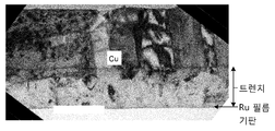
도 5a 및 도 5b는 연속적 Ru 금속 필름 상에 물리 기상 증착(PVD)에 의해 증착된 Cu 시드층을 포함하는 Cu 충진된 트렌치의 단면 투과 전자 현미경(TEM) 사진이다;
도 5c는 본 발명의 일 실시예에 따른 연속적 Ru 필름 상에 도금된 Cu 금속층을 포함하는 Cu 충진된 트렌치의 단면 TEM 사진이다;
도 6은 본 발명의 일 실시예에 따른 Ru 금속 필름을 증착하기 위한 열적 화학 기상 증착(TCVD) 시스템의 개략도이다;
도 7은 본 발명의 다른 실시예에 따른 Ru 금속 필름을 증착하기 위한 다른 TCVD 시스템의 개략도이다; 및
도 8은 본 발명의 실시예들에 따른 Cu 도금 및 어닐링을 위한 프로세싱 시스템의 개략도이다.1A-1L are cross-sectional views of a process for Cu plating on a continuous Ru film in a concave structure in accordance with embodiments of the present invention;
2a and 2b are cross-sectional views of additional concave structures according to an embodiment of the present invention;
3 is a process flow chart for Cu plating on a continuous Ru film in a concave structure in accordance with one embodiment of the present invention;
4 is a process flow chart for Cu plating on a continuous Ru film in a concave structure in accordance with one embodiment of the present invention;
5A and 5B are cross-sectional transmission electron microscopy (TEM) images of Cu filled trenches including Cu seed layers deposited by physical vapor deposition (PVD) on a continuous Ru metal film;
5C is a cross-sectional TEM photograph of a Cu filled trench comprising a Cu metal layer plated on a continuous Ru film according to one embodiment of the present invention;
6 is a schematic of a thermal chemical vapor deposition (TCVD) system for depositing a Ru metal film according to one embodiment of the present invention;
7 is a schematic diagram of another TCVD system for depositing a Ru metal film according to another embodiment of the present invention; And
8 is a schematic diagram of a processing system for Cu plating and annealing according to embodiments of the present invention.
방법들은 이전의(in advanced) 집적 회로들에서 발견된 오목 구조들 중에서 연속적 Ru 금속 필름 상에 다중-단계 Cu 금속 도금을 위해서 제공된다. 고-순도 연속적 Ru 금속 필름의 사용은, 트렌치들 및 비아들과 같은, 높은-종횡-비 오목 구조들의 Cu 금속 충진 동안 바람직하지 않은 마이크로-보이드들의 형성을 방지하고, 상기 연속적 Ru 금속 필름 위에 도금된 연속적 Cu 금속층 (Cu 시드층(seed layer))을 포함하는 큰 Cu 금속 그레인들의 형성을 가능하게 한다. 상기 큰 Cu 그레인들은 상기 Cu 충진된 오목 구조들의 전기적 저항률을 더 낮추고, 상기 집적 회로의 신뢰성을 증가시킨다.Methods are provided for multi-step Cu metal plating on a continuous Ru metal film among concave structures found in in advanced integrated circuits. The use of high-purity continuous Ru metal film prevents the formation of undesirable micro-voids during Cu metal filling of high-vertical-non-concave structures, such as trenches and vias, and plated on the continuous Ru metal film It allows the formation of large Cu metal grains comprising a continuous Cu metal layer (Cu seed layer). The large Cu grains lower the electrical resistivity of the Cu filled concave structures and increase the reliability of the integrated circuit.
본 발명의 하나의 실시예에 따르면, 상기 방법은, 표면 상에 적어도 하나의 오목 구조(recessed feature)가 형성된 기판을 제공하는 단계; 상기 오목 구조 중에, Ru3(CO)12 전구체를 포함하는 프로세스 가스를 사용하는 열적 화학 기상 증착(thermal chemical vapor deposition; TCVD)에 의해 연속적 Ru 금속 필름을 증착하는 단계; 및 상기 연속적 Ru 금속 필름 상에 연속적 Cu 금속층의 증착을 허용하기 위해, Cu 도금조(plating bath)와 상기 연속적 Ru 금속 필름을 접촉시키는 단계, 상기 연속적 Cu 금속층 및 상기 연속적 Ru 금속 필름은 함께 상기 오목 구조의 상기 폭, 깊이 및 부피의 100% 미만으로 충진하는 것을 포함한다. 상기 방법은, 상기 Cu 도금조로부터 상기 기판을 제거하는 단계; 비산화성 가스(non-oxidizing gas) 중에 상기 연속적 Cu 금속층을 어닐링하는 단계; 및 상기 어닐링된 연속적 Cu 금속층 및 상기 어닐링된 추가적 Cu 금속으로부터 형성된 상기 연속적 Ru 금속 필름 상에 큰 Cu 금속 그레인들을 포함하는 상기 오목 구조 중에 적어도 부분적으로 Cu 충진을 형성하기 위해 상기 접촉시키는 단계, 제거하는 단계, 어닐링하는 단계를 반복하는 단계를 더 포함한다. 상기 증착하는 단계는 일산화탄소(CO) 캐리어 가스를 사용하는 TCVD에 의해 실질적으로 산소- 및 카본-프리(oxygen- and carbon-free) 연속적 Ru 필름을 증착하는 단계를 포함할 수 있다.According to one embodiment of the invention, the method comprises the steps of providing a substrate having at least one recessed feature formed on a surface thereof; In the concave structure, depositing a continuous Ru metal film by thermal chemical vapor deposition (TCVD) using a process gas comprising a Ru 3 (CO) 12 precursor; And contacting the continuous Ru metal film with a Cu plating bath to allow deposition of a continuous Cu metal layer on the continuous Ru metal film, wherein the continuous Cu metal layer and the continuous Ru metal film are concave together. Filling to less than 100% of the width, depth and volume of the structure. The method includes removing the substrate from the Cu plating bath; Annealing the continuous Cu metal layer in a non-oxidizing gas; And contacting to form, at least partially, a Cu fill in the concave structure comprising large Cu metal grains on the continuous Ru metal film formed from the annealed continuous Cu metal layer and the annealed additional Cu metal. The method further includes repeating the step of annealing. The depositing may include depositing a substantially oxygen- and carbon-free continuous Ru film by TCVD using a carbon monoxide (CO) carrier gas.
본 발명의 다른 실시예에 따르면, 상기 방법은, 표면 상에 형성된 적어도 하나의 오목 구조를 가지는 기판을 제공하는 단계; 상기 오목 구조 중에, Ru3(CO)12 전구체 및 CO 캐리어 가스를 포함하는 프로세스 가스를 사용하는 TCVD에 의해 실질적으로 산소- 및 탄소-프리(oxygen- and carbon-free) 연속적 Ru 필름을 증착하는 단계; 상기 연속적 Ru 금속 필름 상에 연속적 Cu 금속층의 증착을 허용하기 위해, 제 1 Cu 도금조(plationg bath)와 상기 연속적 Ru 금속 필름을 접촉시키는 단계; 상기 제 1 Cu 도금조로부터 상기 기판을 제거하는 단계; 및 비산화성 가스 중에서 상기 연속적 Cu 금속층을 어닐링하는 단계를 포함한다. 상기 연속적 Cu 금속층 및 연속적 Ru 금속 필름은 상기 오목 구조의 상기 폭, 깊이 및 부피의 100% 미만인 제 1 폭, 깊이 및 부피까지 상기 오목 구조를 함께 충진한다. 상기 방법은, 적어도 부분적으로 상기 오목 구조를 충진하는 추가적 Cu 금속의 증착을 형용하기 위해, 상기 어닐링된 연속적 Cu 금속층과 제 2 Cu 도금조를 접촉시키는 단계; 상기 제 2 Cu 도금조로부터 상기 기판을 제거하는 단계; 및 상기 추가적 Cu 금속을 비산화성 조건들 하에서 어닐링하는 단계를 더 포함한다. 이러한 실시예에 있어서, 상기 추가적 Cu 금속층은 상기 연속적 Cu 금속층 보다 더 빠른 속도로 증착됨으로써, 상기 제 2 Cu 도금조는 상기 제 1 Cu 도금조보다 상이한(different) 화학적 조성을 가지고, 상기 추가적 Cu 금속층은, 상기 제 1 폭, 깊이 및 부피보다 더 크고, 상기 오목 구조의 상기 폭, 깊이 및 부피의 100% 이하인 제 2 폭, 깊이 및 부피까지, 상기 오목 구조를 더 충진하고, 상기 방법은, 상기 연속적 Ru 금속 필름 상에, 상기 어닐링된 연속적 Cu 금속층 및 추가적 Cu 금속으로부터 큰 Cu 금속 그레인들을 형성한다.According to another embodiment of the present invention, the method includes providing a substrate having at least one concave structure formed on a surface; In the concave structure, depositing a substantially oxygen- and carbon-free continuous Ru film by TCVD using a process gas comprising a Ru 3 (CO) 12 precursor and a CO carrier gas. ; Contacting the continuous Ru metal film with a first Cu plating bath to allow deposition of a continuous Cu metal layer on the continuous Ru metal film; Removing the substrate from the first Cu plating bath; And annealing the continuous Cu metal layer in a non-oxidizing gas. The continuous Cu metal layer and the continuous Ru metal film fill the concave structure together to a first width, depth and volume that is less than 100% of the width, depth and volume of the concave structure. The method includes contacting the annealed continuous Cu metal layer with a second Cu plating bath to at least partially deposit a further Cu metal filling the concave structure; Removing the substrate from the second Cu plating bath; And annealing the additional Cu metal under non-oxidizing conditions. In this embodiment, the additional Cu metal layer is deposited at a faster rate than the continuous Cu metal layer, such that the second Cu plating bath has a different chemical composition than the first Cu plating bath, and the additional Cu metal layer is Further filling the concave structure to a second width, depth and volume that is greater than the first width, depth and volume and is no greater than 100% of the width, depth and volume of the concave structure, and the method further comprises the continuous Ru On the metal film, large Cu metal grains are formed from the annealed continuous Cu metal layer and the additional Cu metal.
본 발명의 또 다른 실시예에 따르면, 방법은 부분적으로 제조된 집적 회로 중에 다마신 구조들을 충진하기 위해 제공된다. 상기 방법은, 상기 부분적으로 제조된 집적 회로의 적어도 하나의 오목 구조 중의 확산 베리어 상에, Ru3(CO)12 전구체 및 CO 캐리어 가스를 포함하는 프로세스 가스를 사용하는 TCVD에 의해 실질적으로 산소- 및 탄소-프리 Ru 금속 필름을 증착하는 단계; 및 약 100℃에서 약 500℃까지의 기판 온도 범위에서, 불활성 가스 또는 수소 (H2) 가스, 또는 그들의 조합을 포함하는 비산화성 가스 중에서 상기 연속적 Ru 금속 필름을 어닐링하는 단계를 포함한다. 상기 방법은, 상기 연속적 Ru 금속 필름 상에 연속적 Cu 금속층의 증착을 허용하기 위해서, 제 1 Cu 도금조 중에, 상기 부분적으로 제조된 집적 회로 또는 적어도 일 부분을 침지하는 단계; 상기 제 1 Cu 도금조로부터 상기 부분적으로 제조된 집적 회로를 제거하는 단계; 및 상기 연속적 Cu 금속층을 약 100℃에서 약 500℃까지의 기판 온도 범위에서, 불활성 가스 또는 H2 가스, 또는 그들의 조합을 포함하는 비산화성 가스 중에 어닐링하는 단계를 더 포함한다. 상기 연속적 Cu 금속층 및 연속적 Ru 금속 필름은 함께 상기 오목 구조의 상기 폭, 깊이 및 부피의 100% 미만인 제 1 폭, 깊이 및 부피까지 상기 오목 구조를 충진한다. 상기 방법은, 상기 제 1 폭, 깊이 및 부피 보다 크고 상기 오목 구조의 상기 폭, 깊이 및 부피 이하인 제 2 폭, 깊이 및 부피까지 상기 오목 구조를 적어도 부분적으로 충진하는 추가적인 Cu 금속의 증착을 허용하기 위해서, 제 2 Cu 도금조 중에 상기 부분적으로 제조된 집적 회로, 또는 적어도 일부분을 재-침지하는 단계; 상기 제 2 Cu 도금조로부터 상기 부분적으로 제조된 집적회로를 제거하는 단계; 및 여기서 큰 Cu 금속 그레인들이 상기 어닐링된 연속적 Cu 금속층 및 상기 어닐링된 추가적 Cu 금속으로부터 상기 연속적 Ru 금속 필름 상에 형성됨으로써, 상기 추가적 Cu 금속을 약 100℃에서 약 500℃까지의 기판 온도 범위에서, 불활성 가스 또는 H2 가스, 또는 그들의 조합을 포함하는 비산화성 가스(non-oxidizing gas) 중에 어닐링하는 단계를 더 포함한다.According to another embodiment of the invention, a method is provided for filling damascene structures in a partially fabricated integrated circuit. The method comprises substantially oxygen- and by TCVD using a process gas comprising a Ru 3 (CO) 12 precursor and a CO carrier gas on a diffusion barrier in at least one concave structure of the partially fabricated integrated circuit. Depositing a carbon-free Ru metal film; And annealing the continuous Ru metal film in a non-oxidizing gas comprising an inert gas or hydrogen (H 2 ) gas, or a combination thereof, in a substrate temperature range from about 100 ° C. to about 500 ° C. The method includes immersing the partially fabricated integrated circuit or at least a portion in a first Cu plating bath to permit deposition of a continuous Cu metal layer on the continuous Ru metal film; Removing the partially fabricated integrated circuit from the first Cu plating bath; And annealing the continuous Cu metal layer in a non-oxidizing gas comprising an inert gas or H 2 gas, or a combination thereof, in a substrate temperature range from about 100 ° C. to about 500 ° C. The continuous Cu metal layer and the continuous Ru metal film together fill the concave structure up to a first width, depth and volume that is less than 100% of the width, depth and volume of the concave structure. The method allows for the deposition of additional Cu metal at least partially filling the concave structure up to a second width, depth and volume greater than the first width, depth and volume and less than or equal to the width, depth and volume of the concave structure. Re-immersing said partially fabricated integrated circuit, or at least a portion thereof, in a second Cu plating bath; Removing the partially fabricated integrated circuit from the second Cu plating bath; And wherein large Cu metal grains are formed on the continuous Ru metal film from the annealed continuous Cu metal layer and the annealed additional Cu metal, thereby forming the additional Cu metal in a substrate temperature range of about 100 ° C. to about 500 ° C., Annealing in a non-oxidizing gas comprising an inert gas or H 2 gas, or a combination thereof.
이전의(in advanced) 집적 회로에서 발견된 오목 구조들 중에 연속적 Ru 금속 필름 상에 Cu 금속 도금을 위한 방법은 여러 실시예들에서 기술된다. 연속적 Ru 금속 필름의 사용은, 트렌치들 및 비아들과 같은, 높은-종횡-비 오목 구조들의 Cu 금속 충진 동안 바람직하지 않은 마이크로-보이드들의 형성을 제거하거나 또는 적어도 실질적으로 감소시킨다. 상기 연속적 Ru 금속 필름은, 상기 오목 구조들 중의 상기 연속적 Ru 금속 필름 상에 도금된 얇은 연속적 Cu 금속층에 뛰어난 연속적 접착을 제공한다. 상기 연속적 접착은, 상기 오목 구조 안으로 개선된 Cu 그레인 침투 및 상기 연속적 Cu 금속층을 포함하는, 상기 오목 구조들 중에 전체 Cu 금속을 포함시킨, 큰 Cu 그레인들의 성장을 위해 예외적으로 허용한다. 상기 큰 Cu 그레인들은 상기 Cu 충진된 오목 구조들의 전기 저항률을 더 낮추고, 상기 집적 회로의 신뢰성을 증가시킨다.Among the concave structures found in in advanced integrated circuits, a method for plating Cu metal on a continuous Ru metal film is described in various embodiments. The use of a continuous Ru metal film eliminates or at least substantially reduces the formation of undesirable micro-voids during Cu metal filling of high-vertical-non-concave structures, such as trenches and vias. The continuous Ru metal film provides excellent continuous adhesion to a thin continuous Cu metal layer plated on the continuous Ru metal film of the concave structures. The continuous adhesion allows exceptionally for improved Cu grain penetration into the concave structure and the growth of large Cu grains, including the entire Cu metal in the concave structures, including the continuous Cu metal layer. The large Cu grains further lower the electrical resistivity of the Cu filled concave structures and increase the reliability of the integrated circuit.
본 발명의 실시예들은 도 1 내지 도 8과 관련하여 여기에 기술된다. 집적 회로 디바이스들에서 발견된 오목 구조들을 도시하는 도 1 및 도 2는 실제 집적 회로 디바이스의 임의의 특별한 부분의 실제 배치도(plan) 또는 단면도로 의도되지 않는다는 것을 이해하여야 하다. 상기 실제 디바이스들에서, 상기 필름들 및 층들은 규칙적이지 않을 수 있고, 두께가 다양한 비율들을 가질 수 있다. 그 보다, 상기 도면들은, 실제 가능한 형태보다도, 본 발명의 실시예들을 더 명확하고 완전하게 설명하는 이상화된 대표적 예시들을 보여준다.Embodiments of the invention are described herein in connection with FIGS. 1 to 8. 1 and 2 showing concave structures found in integrated circuit devices are not intended to be actual plan or cross-sectional views of any particular portion of the actual integrated circuit device. In the actual devices, the films and layers may not be regular and may have ratios of varying thickness. Rather, the figures show idealized representative examples that more clearly and completely describe embodiments of the present invention than are actually possible.
또한, 상기 도면들은 본 발명의 실시예들을 이용하여 제조될 수 있는 디바이스들의 셀 수 없이 많은 변경들 중 단지 하나를 나타낸다. 프로세스들은 도 1 내지 도 8을 참조하여 명세서에서 기술된다; 그럼에도 불구하고, 본 발명의 실시예에 따른 방법들은 여기에서 상세히 기술된 것들로부터 매우 다른 구조들, 시스템들 및 제조 프로세스들을 이용하여 실시될 수 있다는 것이 명백하다. 여기에서 기술된 실시예들은 예시적이고, 본 발명의 범위를 제한하여서는 안되며, 그것이 아래의 청구항에서 정의된다. In addition, the figures show just one of countless variations of devices that can be fabricated using embodiments of the present invention. Processes are described in the specification with reference to FIGS. 1 to 8; Nevertheless, it is clear that the methods according to the embodiment of the present invention can be carried out using very different structures, systems and manufacturing processes from those described in detail herein. The embodiments described herein are exemplary and should not limit the scope of the invention, which is defined in the claims below.
"일 실시예" 또는 "하나의 실시예" 의미들에 대해 이 명세서를 통한 참조는, 상기 실시예와 관련하여 기술된 특정한 특징, 구조, 물질, 또는 특성이 본 발명의 적어도 하나의 실시예에서 포함된다는 것을 의미하지만, 그들이 모든 실시예에 존재하는 것을 나타내지 않는다. 그러므로, 이 명세서를 통해 다양한 장소에서 "일 실시예에 있어서" 또는 "하나의 실시예에 있어서"의 상기 구문들의 출현들은 반드시 본 발명의 동일한 실시예를 언급하고 있지는 않다.Reference throughout this specification to the meanings of “one embodiment” or “one embodiment” indicates that a particular feature, structure, material, or characteristic described in connection with the embodiment is in at least one embodiment of the invention. It is meant to be included, but does not indicate that they are present in all embodiments. Therefore, the appearances of the above phrases in "in one embodiment" or "in an embodiment" in various places throughout this specification are not necessarily referring to the same embodiment of the invention.
도 1a는 종래 기술에 알려진 바와 같이, 단순화된 오목 구조의 개략도이다.1A is a schematic diagram of a simplified concave structure, as known in the art.
도 1b 내지 도 1l은 본 발명의 실시예들 따른 오목 구조에서 연속적 Ru 필름 상에 Cu 도금을 위한 프로세스의 단면도를 나타낸다.1B-1L illustrate cross-sectional views of a process for Cu plating on a continuous Ru film in a concave structure in accordance with embodiments of the present invention.
도 1a는 제조의 중간 단계(intermediate phase)에서 집적 회로 형성의 부분(205)의 단면도를 개략적으로 나타낸다. 상기 부분(205)은 표면(203)을 가진 오목 구조(206)를 포함하는 층(210)을 나타낸다. 상기 층(210)은, 예를 들어, Si 기판 또는 절연체층을 포함할 수 있다. 절연체층(210)은, 예를 들어, SiO2, 플루오르화 실리콘 글라스(fluorinated silicon glass; FSG), 탄소 도프된 실리콘 산화막(carbon doped silicon oxide) (즉, CORALTM), 탄소-도프된 실리콘 질화물, SiCOH 또는 SiCOH-함유 로우-k 물질, 비-다공성 로우-k 물질, 다공성 로우-k 물질, CVD 로우-k 물질, 스핀-온 절연체 (SOD) 로우-k 물질과 같은 로우 절연 상수 (로우-k) 절연체, 또는 임의의 다른 적절한 절연 물질을 포함할 수 있다. 절연체층(210)은 또한 실리콘-함유 절연체 물질을 대신하거나 또는 비-실리콘-함유 로우-k 절연 물질을 첨가하는 것을 포함할 수 있다; 예를 들어, SILK™와 같은, 상업적으로 이용 가능한 폴리머-기반된 탄소-수소-산소-함유 절연체 물질.1A schematically illustrates a cross-sectional view of a
상기 오목 구조(206)는, 약 2:1이상, 예를 들어, 3:1, 4:1, 5:1, 6:1, 12:1, 15:1, 또는 더 높은 종횡비를 가지는 트렌치 또는 비아(via)일 수 있다. 상기 트렌치/비아는 약 200 nm 이하, 예를 들어, 150 nm, 100 nm, 65 nm, 45 nm, 32 nm, 22 nm, 또는 이하의 폭을 가질 수 있다. 그러나, 본 발명의 실시예들은 다른 종횡비 및 트렌치/비아 폭이 이용될 수 있는 것과 같이, 이러한 종횡비 또는 트렌치/비아 폭에 제한되지 않는다. 명료성을 위해, 도 1a에 단지 하나의 오목 구조(206)만 도시될지라도, 당업계의 숙련된 자들은 종래의 집적 회로들이 수많은 오목 구조를 포함하고, 본 발명의 실시예들은 임의의 많은 오목 구조들을 포함하는 집적 회로들에 쉽게 적용할 수 있다는 것을 쉽게 깨달을 것이다. 오목 구조들의 추가적 실시예들은 도 2a 및 도 2b에 나타난다.The
도 1b는 도 1a의 상기 오목 구조(206) 중에 형성된 확산 배리어 필름(212)을 포함하는 오목 구조(207)를 나타낸다. 상기 확산 배리어 필름(212)은, 예를 들어, 탄탈륨(Ta)-함유 필름 (즉, 탄탈륨 (Ta), 탄탈륨 나이트라이드 (TaN), 탄탈륨 카바이드 (TaC), 또는 탄탈륨 카보나이트라이드 (TaCN)), 티타늄 (Ti)-함유 필름 (즉, 티타늄 (Ti), 티타늄 나이트라이드 (TiN), 티타늄 카바이드 (TiC), 또는 티타늄 카보나이트라이드 (TiCN)), 또는 텅스텐 (W)-함유 필름 (즉, 텅스텐 (W), 텅스텐 나이트라이드 (WN), 텅스텐 카바이드 (WC), 또는 텅스텐 카보나이트라이드 (WCN)), 또는 그들의 조합을 포함할 수 있다. 상기 조합은 독립된 Ta, TaN, Ti, TiN, 및 WN 필름들의 둘 이상인, 예를 들어, Ta/TaN, Ti/TiN, TaN/TiN 또는 TaN/WN을 포함할 수 있다. 상기 확산 배리어 필름(212)의 두께는 예를 들어, 약 1 nm 및 약 10 nm 사이, 또는 약 2 nm 및 약 5 nm 사이, 예를 들어, 약 4 nm일 수 있다. 상기 확산 배리어 필름(212)은 당업계에서 통상의 지식을 가지 자에 의해 알려진 다양한 다른 증착 방법에 의해 필름 증착 시스템에서 증착될 수 있고, 제한되는 것은 아니지만, PVD, 이온화된 PVD (ionized PVD; iPVD), TCVD, 펄스화된 CVD (pulsed CVD), 플라즈마-강화된 CVD (plasma-enhanced CVD; PECVD), ALD, 플라즈마-강화된 ALD (plasma-enhanced ALD; PEALD), 또는 스퍼터링 방법들을 포함할 수 있다. 하나의 실시예에 있어서, 상기 확산 배리어 필름(212)은 상기 높은-종횡-비 오목 구조(207) 중에 적합하게 형성될 수 있다.FIG. 1B shows a
다양한 Ta-, Ti-, 및 W-함유 전구체들은 상기 확산 배리어 필름(212)을 증착하기 위해 이용될 수 있다. Ta-함유 전구체들의 대표적인 예들은, Ta(NMe2)5 (펜타키스(디메틸아미도)탄탈륨, PDMAT), Ta(NEtMe)5 (펜타키스(에틸메틸아미도)탄탈륨, PEMAT), (tBuN)Ta(NMe2)3 (터트-부틸이미도 트리스(디메틸아미도)탄탈륨, TBTDMT), (tBuN)Ta(NEt2)3 (터트-부틸이미도 트리스(디에틸아미도)탄탈륨, TBTDET), (tBuN)Ta(NEtMe)3 (터트-부틸이미도 트리스(에틸메틸아미도)탄탈륨, TBTEMT), (EtMe2CN)Ta(NMe2)3 (터트--아밀이미도 트리스(디메틸아미도)탄탈륨, TAIMATA), (iPrN)Ta(NEt2)3 (이소프로필이미도 트리스(디에틸아미도)탄탈륨, IPTDET), Ta2(OEt)10 (탄탈륨 펜타-에톡사이드, TAETO), (Me2NCH2CH2O)Ta(OEt)4 (디메틸아미노에톡시 탄탈륨 테트라-에톡사이드, TATDMAE), 및 TaCl5 (탄탈륨 펜타클로라이드)를 포함한다. Ti-함유 전구체들의 대표적인 예들은, Ti(NEt2)4 (테트라키스(디에틸아미도) 티타늄, TDEAT), Ti(NMeEt)4 (테트라키스(에틸메틸아미도)티타늄, TEMAT), Ti(NMe2)4 (테트라키스(디메틸아미도)티타늄, TDMAT), Ti(THD)3 (트리스(2,2,6,6-테트라메틸-3,5-헵타네디오나토)티타늄), 및 TiCl4 (티타늄 테트라클로라이드)를 포함한다. W-함유 전구체들의 대표적인 예들은, w(CO)6 (텅스텐 헥사카보닐), WF6 (텅스텐 헥사플루오라이드), 및 (tBuN)2W(NMe2)2 (비스(터트-부틸이미도)비스(디메틸아미도)텅스텐, BTBMW)을 포함한다. 상기의 전구체들에 있어서, 다음 약어들이 사용된다: ME: 메틸; Et: 에틸; iPr: 이소프로필; tBu: 터트-부틸; 및 THD : 2,2,6,6-테트라메틸-3,5-헵탄디오네이트. 몇몇 실시예들에 있어서, 암모니아 (NH3) 또는 히드라진 (N2H4)과 같은, 질소-함유 가스가 상기 확산 배리어 필름(212)을 증착할 때 질소의 소스로서 이용될 수 있다. 본 발명의 몇몇 실시예들에 따르면, 상기 확산 배리어 필름(212)은 생략될 수 있다.Various Ta-, Ti-, and W-containing precursors may be used to deposit the
도 1c는 상기 오목 구조(207)의 선택적 확산 배리어 필름(212) 상에 형성된 Ru 금속 필름(214)을 포함하는 오목 구조(208)를 나타낸다. 상기 Ru 금속 필름(214)의 두께는, 예를 들어, 약 0.5 nm에서 약 10 nm까지의 범위에, 약 2 nm에서 약 5 nm까지의 범위에, 또는 약 3 nm에서 약 4 nm까지의 범위에, 예를 들어, 약 2 nm에 있을 수 있다.1C shows a
상기 Ru 금속 필름(214)은 Ru3(CO)12 전구체 및 CO 캐리어 가스를 사용하는 CVD 또는 TCVD 프로세스 중에서 증착될 수 있다. 상기 CO 캐리어 가스는, 금속 전구체 기화(vaporization) 시스템에서 기판 상에 Ru 금속 필름을 증착하기 위해 형성된 프로세스 챔버로 Ru3(CO)12 전구체 증기의 효율적인 전송을 위해 이용될 수 있다. 상기 CO 캐리어 가스의 사용은, 상기 금속 전구체 기화 시스템에서 그리고 상기 금속 전구체 기화 시스템 및 상기 Ru 금속 증착 챔버 사이의 가스 라인들에서, 상기 Ru3(CO)12 전구체의 조기 분해(premature decomposition)를 방지하거나 최소로 함으로써 반도체 제조를 위해 요구된 높은 Ru3(CO)12 전구체 증기 전송 속도를 가능하게 한다. Ru3(CO)12 전구체 및 CO 캐리어 가스를 사용하는 예시적 Ru TCVD 프로세스들은 미국 특허 제 7,270,848 호 및 제 7,279,421 호에서 기술되며, 그것의 전체 내용은 참고로서 여기에 통합된다.The
Ru 금속 필름(214)을 증착하기 위한 프로세싱 조건들은 약 100℃에서 약 400℃까지, 또는 150℃에서 약 250℃까지의 기판 온도 범위, 그리고 약 0.1 mTorr에서 약 200 mTorr까지, 약 5 mTorr에서 약 200 mTorr까지, 또는 약 50 mTorr에서 약 150 mTorr까지의 증착 챔버 압력 범위를 포함할 수 있다. 상기 금속 전구체 기화 시스템 중에서 기화되는 상기 고체 Ru3(CO)12 전구체는, 약 40℃에서 약 150℃까지, 또는 약 60℃ 및 약 90℃ 사이의 온도 범위에서 유지될 수 있다. 하나의 실시예에 있어서, 상기 Ru 금속 증착 조건들은 약 80℃ 이하의 온도에서 상기 고체 Ru3(CO)12 전구체를 유지하고, 약 100 mTorr의 증착 챔버 압력을 유지하고, 그리고 약200℃의 기판 온도를 유지하는 것을 포함할 수 있다.Processing conditions for depositing the
TCVD 프로세스 중에서 상기 Ru3(CO)12 전구체의 사용은 반도체 제조에 상당히 적합한, 실질적으로 산소- 및 탄소-프리 연속적 Ru 금속 필름들의 증착을 가능하게 한다. 하나의 실시예에 있어서, 2 nm 두께 Ru 금속 필름은 TaN 필름 상에 증착되었다. 상기 Ru 금속 필름은 2차 이온 질량 분석법(secondary ion mass spectroscopy; SIMS)에 의해 측정된 것과 같이, 약 0.1% 레벨의 산소 및 탄소 불순물, X-선 회절(X-ray diffraction; XRD)에 의해 측정된 것과 같이, 약 1.9 nm의 평균 Ru 금속 그레인 크기, 및 원자힘 현미경(atomic force microscope; AFM)에 의해 측정된 것과 같이, 약 0.63 nm의 제곱 평균(root mean square; rms) 표면 거칠기를 가졌다.The use of the Ru 3 (CO) 12 precursor during the TCVD process allows the deposition of substantially oxygen- and carbon-free continuous Ru metal films, which is quite suitable for semiconductor fabrication. In one embodiment, a 2 nm thick Ru metal film was deposited on a TaN film. The Ru metal film was measured by oxygen and carbon impurities, X-ray diffraction (XRD) at a level of about 0.1%, as measured by secondary ion mass spectroscopy (SIMS). As such, it had an average Ru metal grain size of about 1.9 nm, and a root mean square (rms) surface roughness of about 0.63 nm, as measured by an atomic force microscope (AFM).
본 발명의 몇몇 실시예들에 따르면, 상기 증착된 Ru 금속 필름(214)은 산소 및 탄소 불순물들을 더 감소시키고, 상기 Ru 금속 필름(214)의 물질 특성들을 개선하는 비산화성 가스 중에서 선택적으로 어닐링될 수 있다. 도 1d에서, 화살표들(216)은 Ru 금속 필름(214)의 어닐링을 나타낸다. 상기 비산화성 가스는 불활성 가스(inert gas), 수소 (H2) 가스 또는 그들의 조합을 포함할 수 있다. 하나의 실시예에 있어서, 상기 Ru 금속 필름(214)은, H2 가스로 구성되거나, 또는 H2 가스 및 불활성 가스의 조합으로 구성된 H2-함유 가스 중에서 어닐링될 수 있다. 상기 불활성 가스는 질소(N2) 가스 및 비활성 가스(noble gas) (즉, He, Ne, Ar, Kr, 및 Xe )들로부터 선택될 수 있다. 뿐만 아니라, 상기 H2-함유 가스는 여기된 플라즈마 또는 여기되지 않은 플라즈마일 수 있다. H2 및 불활성 가스의 조합들은, 예를 들어, 90% H2 이하, 예를 들어, 80%, 60%, 20%, 10%, 5%, 또는 그 이하와, 밸런스(balance) 불활성 가스를 포함할 수 있다. 상기 H2-함유 가스는 형성 가스(forming gas)를 포함하거나 또는 형성 가스(forming gas)로 이루어질 수 있다. 형성 가스는 보통 약 10% 미만의 H2, 밸런스 N2 (less that about 10% H2, balance N2)를 포함한다. 예시적 어닐링 조건들은, 약 1 Torr에서 약 1000 Torr까지, 또는 약 10 Torr에서 약 100 Torr까지의 가스 압력 범위, 약 100℃에서 약 500℃까지, 또는 약 200℃에서 약 400℃까지의 기판 온도 범위 및 약 1 분에서 약 30분까지의 어닐링 시간 범위를 더 포함할 수 있다. 그러나, 본 발명의 실시예들은 다른 어닐링 조건들이 이용될 수 있는 것처럼 이러한 조건들에 의해 제한되지 않는다. 본 발명의 몇몇 실시예들에 있어서, 상기 가스 압력은 약 0.1 Torr에서 약 100 Torr까지, 또는 약 0.5 Torr에서 약 10 Torr까지의 범위에 있을 수 있다. 하나의 실시예에 있어서, 상기에 기술된 상기 2 nm 두께 Ru 금속 필름은 1.5 Torr 및 400℃에서 10 분 동안 형성 가스 중에서 어닐링되었고, 이러한 처리는 0.1% 미만 레벨의 산소- 및 탄소-불순물을 더 감소시켰다. 게다가, 상기 평균 Ru 금속 그레인 크기가 2.4 nm까지 증가되었고, 상기 RMS 표면 거칠기는 0.5 nm까지 감소되었다.According to some embodiments of the invention, the deposited
도 1e는 본 발명의 실시예들에 따른 도 1d 또는 1c의 상기 오목 구조(208)의 상기 연속적 Ru 금속 필름(214) 상에 도금된 연속적 Cu 금속층(228)을 포함하는 오목 구조(209)를 나타낸다. 상기 연속적 Cu 금속층(228)은, Cu 도금 및 어닐링을 위해 설정된(configured) 프로세싱 시스템에서 제 1 Cu 도금조와 상기 연속적 Ru 금속 필름(214)을 접촉시킴으로써 형성될 수 있다. 상기 Cu 도금 프로세스는 전기화학적 Cu 도금 프로세스 또는 무전해 Cu 도금 프로세스일 수 있다. 상기 연속적 Cu 금속층(228)은 약 1 nm에서 약 50 nm까지의 범위, 약 2 nm에서 약 20 nm까지의 범위, 또는 약 2 nm에서 약 10 nm까지의 두께 범위를 가질 수 있다. 몇몇 실시예들에 있어서, 상기 연속적 Cu 금속층(228)은 약 2.5 nm 또는 약 4 nm의 두께를 가질 수 있다. 본 발명의 실시예들에 따르면, 단지 상기 연속적 Cu 금속층(228)이 도 1e에 도시된 것처럼 Cu 금속으로 상기 오목 구조(209)를 부분적으로 충진한다. 상기 연속적 Cu 금속층(228)의 형성 후에, 상기 부분(205)은 상기 제 1 Cu 도금조로부터 제거된다.1E illustrates a
본 발명의 몇몇 실시예들에 따르면, 상기 Ru 금속 필름(214)의 두께 및/또는 상기 연속적 Cu 금속층(228)의 두께는 상기 오목 구조(206)의 폭과 작게 비교될 수 있다. 이것은 하나 이상의 후속 Cu 도금 단계들 중에서 상기 오목 구조(209)의 보이드-프리 충진을 허용한다. 예를 들어, 상기 Ru 금속 필름(214)을 위해 약 2 nm에서 약 5 nm까지의 두께 범위에서, 그리고 약 2 nm에서 약 10 nm까지의 범위에서, 결합된 상기 Ru 금속 필름(214) 및 상기 연속적 Cu 금속층(228)의 두께는, 약 4 nm 및 약 15 nm 사이이다. 그러므로, 상기 오목 구조(206)에 대한 45 nm의 폭을 위해, 상기 결합된 Ru 금속 필름(214) 및 오목 구조(209)의 연속적 Cu 금속층(228)은 상기 오목 구조(206)의 폭의 약 18% 및 약 67% 사이를 차지한다. 상기 Ru 금속 필름(214)을 위한 약 2 nm에서 약 5 nm까지의 두께 범위를 위해, 그리고 약 2.5 nm에서 약 4 nm까지의 범위에서 상기 연속적 Cu 금속층(228)의 두께를 위해, 상기 결합된 Ru 금속 필름(214) 및 오목 구조(209)의 연속적 Cu 금속층(228)은 상기 오목 구조(206)의 상기 폭의 약 20% 및 약 40% 사이를 차지한다. 비슷한 계산들은 상기 오목 구조(206)의 다른 폭, 예를 들어, 32 nm 및 22 nm 폭을 위해 행해질 수 있다. 본 발명의 몇몇 실시예들에 따르면, 상기 결합된 Ru 금속 필름(214) 및 연속적 Cu 금속층(228)은, 약 50% 미만, 약 40% 미만, 약 30% 미만, 또는 심지어 상기 오목 구조(206)의 폭의 약 20% 미만을 차지할 수 한다. 유사하게, 상기 오목 구조(206)의 상기 깊이 및 상기 부피에 관하여, 상기 Ru 금속 필름(214) 및 연속적 Cu 금속층(228)은, 상기 오목 구조(206)의 상기 깊이 및 상기 부피의 100% 미만, 예를 들어, 약 50% 미만, 약 40% 미만, 약 30% 미만, 또는 심지어 상기 오목 구조(206)의 상기 깊이 및 상기 부피의 약 20% 미만으로 함께 차지한다.According to some embodiments of the present invention, the thickness of the
본 발명의 실시예들에 따르면, 상기 연속적 Cu 금속층(228)의 증착 후에, 상기 부분(205)은 불순물들을 감소시키고, Cu 그레인 사이즈를 증가시키는 것을 포함하는, 상기 연속적 Cu 금속층(228)의 물질 특성을 개선하기 위한 비산화성 가스에서 어닐링될 수 있다. 도 1f에서, 화살표들(236)은 연속적 Cu 금속층(228)의 어닐링을 나타낸다. 하나의 실시예에 있어서, 상기 연속적 Cu 금속층(228)은 H2 가스의 구성, 또는 H2 가스 및 불활성 가스의 조합의 구성인 H2-함유 가스에서 어닐링될 수 있다. 상기 불활성 가스는 N2 가스 및 상기 비활성 가스(noble gas) (즉, He, Ne, Ar, Kr, 및 Xe)들로부터 선택될 수 있다. 뿐만 아니라, 상기 H2-함유 가스는 여기된 플라즈마 또는 여기되지 않은 플라즈마일 수 있다. H2 및 불활성 가스의 조합들은, 예를 들어, 90% H2 이하, 예를 들어, 80%, 60%, 20%, 10%, 5%, 또는 그 이하와 밸런스 불활성 가스를 포함할 수 있다. 상기 H2-함유 가스는 형성 가스(forming gas)를 포함하거나 또는 형성 가스로 이루어질 수 있다. 형성 가스는 보통 약 10% 미만의 H2, 밸런스 N2를 포함한다. 예시적 어닐링 조건들은, 약 1 Torr에서 약 1000 Torr까지, 또는 약 10 Torr에서 약 100 Torr까지의 가스 압력 범위, 약 100℃에서 약 500℃까지, 또는 약 200℃에서 약 400℃까지의 기판 온도 범위 및 약 1 분에서 약 30분까지의 어닐링 시간 범위를 더 포함할 수 있다. 그러나, 본 발명의 실시예들은 다른 어닐링 조건들이 이용될 수 있는 것처럼 이러한 조건들에 의해 제한되지 않는다. 본 발명의 몇몇 실시예들에 있어서, 상기 가스 압력은 약 0.1 Torr에서 약 100 Torr까지, 또는 약 0.5 Torr에서 약 10 Torr까지의 범위에 있을 수 있다.According to embodiments of the present invention, after deposition of the continuous
본 발명의 실시예들에 따르면, 상기 연속적 Cu 금속층(228)을 포함하는 상기 부분(205)의 어닐링 후에, 추가적 Cu 금속층(230)은 제 2 Cu 도금조 중에서 상기 어닐링된 연속적 Cu 금속층(248) 상에 도금된다. 도 1g에 도시된 예시적 실시예에 있어서, 상기 추가적 Cu 금속층(230)은 상기 오목 구조(209)를 충진하고, 상기 오목 구조 중에 더 낮은 추가적 Cu 금속 부분(235) 및 상기 오목 구조(209)의 개구부 밖(outside)에 상부 추가적 Cu 금속 부분(240)을 포함한다. 상기 상부 추가적 Cu 금속 부분(240)의 두께는 100 nm에서 2000 nm까지의 범위에, 또는 250 nm 및 750 nm까지의 범위에 있을 수 있다.According to embodiments of the present invention, after annealing of the
본 발명의 몇몇 실시예들에 따르면, 상기 제 1 및 제 2 Cu 도금조들은 동일한 것일 수 있다. 다른 실시예들에 따르면, 상기 제 1 및 제 2 Cu 도금조는 상이한 화학적 조성들을 가질 수 있다. 상기 화학적 조성들은, 예를 들어, 환원 작용제 농도, 계면 활성제 농도, 및 구리 이온들의 소스들 및 농도의 하나 이상과 상이할 수 있다. 본 발명의 몇몇 실시예들에 따르면, 상기 제 2 Cu 도금조는 상기 제 1 Cu 도금조보다 더 높은 Cu 이온의 농도를 포함하기 위해 형성되고, 상기 제 1 Cu 도금조보다 더 빠른 속도로 오목 구조 중에서 Cu 금속을 도금할 수 있다.According to some embodiments of the present invention, the first and second Cu plating baths may be the same. According to other embodiments, the first and second Cu plating baths may have different chemical compositions. The chemical compositions may differ, for example, from one or more of reducing agent concentration, surfactant concentration, and sources and concentrations of copper ions. According to some embodiments of the present invention, the second Cu plating bath is formed to contain a higher concentration of Cu ions than the first Cu plating bath, and is formed in a concave structure at a faster rate than the first Cu plating bath. Cu metal may be plated.
상기 추가적 Cu 금속층(230)의 증착 후에, 상기 부분(205)은 상기 추가적 Cu 금속층(230)의 물질 특성들을 더 개선하기 위해 비산화성 가스중에서 어닐링될 수 있다. 상기 어닐링은 상기 추가적 Cu 금속층(230) 중에 큰 Cu 그레인들을 형성한다. 도 1h에서, 화살표들(246)은 상기 추가적 Cu 금속층(230)의 어닐링 또는 열-처리를 나타낸다. 상기 비산화성 가스는 불활성 가스, H2 가스, 또는 그들의 조합을 포함할 수 있다. 하나의 실시예에 있어서, 상기 추가적 Cu 금속층(230)은 H2 가스로 구성되거나, 또는 H2 가스 및 불활성 가스의 조합으로 구성된 H2-함유 가스 중에서 어닐링될 수 있다. 상기 불활성 가스는 질소(N2) 상기 비활성 가스(noble gas) (즉, He, Ne, Ar, Kr, 및 Xe)들로부터 선택될 수 있다. 뿐만 아니라, 상기 H2-함유 가스는 여기된 플라즈마 또는 여기되지 않은 플라즈마일 수 있다. H2 및 불활성 가스의 조합들은, 예를 들어, 90% H2 이하, 예를 들어, 80%, 60%, 20%, 10%, 5%, 또는 그 이하와 밸런스 불활성 가스를 포함할 수 있다. 상기 H2-함유 가스는 형성 가스(forming gas)를 포함하거나 또는 형성 가스로 이루어질 수 있다. 예시적 어닐링 조건들은, 약 1 Torr에서 약 1000 Torr까지, 또는 약 10 Torr에서 약 100 Torr까지의 가스 압력 범위, 약 100℃에서 약 500℃까지, 또는 약 200℃에서 약 400℃까지의 기판 온도 범위, 및 약 1 분에서 약 30분까지의 어닐링 시간 범위를 더 포함할 수 있다. 그러나, 본 발명의 실시예들은 다른 어닐링 조건들이 이용될 수 있는 것처럼 이러한 조건들에 의해 제한되지 않는다. 본 발명의 몇몇 실시예들에 있어서, 상기 가스 압력은 약 0.1 Torr에서 약 100 Torr까지, 또는 약 0.5 Torr에서 약 10 Torr까지의 범위에 있을 수 있다.After deposition of the additional
도 1i는 상기 어닐링 후에 어닐링된 추가적 Cu 금속층(232)을 개략적으로 나타낸다. 상기 어닐링된 추가적 Cu 금속층(232)은, 상기 오목 구조 중에서 더 낮게 어닐링된 Cu 금속 부분(237) 및 상기 오목 구조(209)의 개구부 밖에 상부 어닐링된 Cu 금속 부분(242)을 포함한다. 상기 어닐링된 추가적 Cu 금속층(232)은 상기 어닐링된 연속적 Cu 금속층(228)으로부터 상기 Cu 물질을 포함하는 큰 Cu 그레인(233)들을 포함한다. 다시 말하면, 상기 큰 Cu 그레인들(233)의 성장은, 단지 상기 추가적 Cu 금속층(232)으로부터 뿐만 아니라, 상기 전체 오목 구조(209)를 통해 상기 연속적 Ru 금속 필름(214) 상에 형성한 상기 Cu 그레인들(233)과 같은 상기 연속적 Cu 금속층(228)으로부터 있다. 상기 어닐링에 의한 상기 전체 오목 구조(209) 중에서 상기 큰 Cu 그레인들(233)의 형성은, 상기 연속적 Cu 금속층(228)과 상기 연속적 Ru 금속 필름(214)에 대한 그것의 뛰어난 연속적 접착에 의해 가능해진다. 일반적으로, 상기 오목 구조 중에서 상기 큰 Cu 그레인들(233)의 크기는 상기 상부 어닐링된 Cu 금속 부분(242)의 증가된 두께와 증가된다고 관찰되었다.1I schematically shows an additional
도 1j는, 상기 상부 어닐링된 Cu 금속 부분(242) 및 상기 어닐링된 확산 배리어 필름(212)과 연속적 Ru 금속 필름(214)의 부분들이, 평탄화된 표면(250)을 형성하기 위해, 일반적으로 화학 기계적 연마(chemical mechanical polishing; CMP) 방법에 의해 제거된, 부분(205)을 나타낸다.1J illustrates that the top annealed
도 1e, 도 1f 및 도 1k를 지금 참조하여, 본 발명의 다른 실시예들에 따르면, 상기 연속적 Cu 금속층(228)의 어닐링 후에, 상기 추가적 Cu 금속의 상기 도금은 단지 부분적으로 오목 구조(209)를 충진할 수 있다. 도 1k는 Cu 도금 프로세스 후에 추가적 Cu 금속층(230a)을 포함하는, 부분적으로 충진된 오목 구조(211)를 나타낸다. 본 발명의 실시예들에 따르면, 상기 추가적 Cu 금속을 도금함으로써 Cu 금속으로 충진되는 도 1k에 있는 오목 구조(211)의 깊이 및/또는 부피의 퍼센트는, 약 50% 미만, 약 40% 미만, 약 30% 미만, 20% 미만, 또는 심지어 약 10% 미만일 수 있다. 상기 추가적 Cu 금속층(230a)의 Cu 도금은 상기 오목 구조(211)를 더 충진하기 위한 다수 회 반복될 수 있다. 각각의 도금 프로세스는 비산화성 가스를 사용하는 어닐링 프로세스가 이어질 수 있다.Referring now to FIGS. 1E, 1F and 1K, in accordance with other embodiments of the present invention, after annealing of the continuous
도 1e, 도 1f 및 도 1l을 참조하여, 본 발명의 다른 실시예들에 따르면, 상기 연속적 Cu 금속층(228)의 어닐링 후에, 추가적 Cu 금속의 도금은 실질적으로 오목 구조(209)를 충진할 수 있다. 도 1l은 Cu 도금 프로세스 후에 추가적 Cu 금속층(230b)을 포함한, 실질적으로 충진된 오목 구조(213)를 나타낸다. 본 발명의 실시예들에 따르면, 상기 추가적 Cu 금속을 도금함으로써 Cu 금속으로 충진되는 도 1l에 있는 오목 구조(213)의 깊이 및/또는 부피의 비율(percentage)은 약 50% 초과, 약 60% 초과, 약 70% 초과, 약 80% 초과, 또는 심지어 90% 초과일 수 있다. 상기 추가적 Cu 금속층(230b)의 Cu 도금은 오목 구조(213)을 더 충진하기 위해 다수 회 반복될 수 있다. 각각의 도금 프로세스는 비산화성 가스를 사용하는 어닐링 프로세스가 이어진다.1E, 1F, and 1L, in accordance with other embodiments of the present invention, after annealing the continuous
그러므로, 모든 실시예들에 있어서, 상기 오목 구조를 충진한 상기 추가적 Cu 금속층(230, 230a, 230b)은, 상기 연속적 Ru 금속 필름(214) 및 연속적 Cu 금속층(228)은, 제 1 폭, 깊이 및 부피보다 더 큰 제 2 폭, 깊이, 및 부피까지 상기 오목 구조를 더 충진하기 위해 도금된다. 상기 오목 구조까지 더 충진된 제 2 폭, 깊이, 및 부피는 상기 오목 구조의 폭, 깊이, 및 부피의 100% 이하일 수 있다. 게다가, 상기 제 2 폭, 깊이, 및 부피는 100% 미만일 수 있고, 상기 방법은, 예를 들어, 상기 오목 구조의 폭, 깊이, 및 부피의 약 90% 내지 약 100%까지, 상기 오목 구조가 제 3 폭, 깊이, 및 부피가 달성되기까지 1회 이상의 원하는 Cu 금속의 도금 시간 추가 및 어닐링의 반복을 더 포함할 수 있다. 하나의 실시예에 있어서, 상기 제 1 폭, 깊이, 및 부피는 상기 오목 구조의 폭, 깊이, 및 부피의 약 20%미만이고, 상기 제 2 폭, 깊이, 및 부피는 상기 오목 구조의 폭, 깊이, 및 부피의 약 20% 초과 및 약 50% 미만이고, 및 상기 제 3 폭, 깊이, 및 부피는 상기 오목 구조의 폭, 깊이, 및 부피의 약 100% 이다.Therefore, in all embodiments, the additional Cu metal layers 230, 230a, 230b filling the concave structure, the continuous
단순화된 오목 구조(206)는 도 1a에 도시되고 상기에 기술되었지만, 본 발명의 실시예들은 집적 회로 설계에서 발견된 다른 유형들의 오목 구조에 적용될 수 있다. 도 2a 및 도 2b는 본 발명의 실시예들이 구현될 수 있는 당업계에 알려져 있는 다른 오목 구조들의 단면도를 개략적으로 나타낸다. 도 2a 및 도 2b에 도시된 상기 패터화된 구조들을 형성하기 위한 프로세싱 방법들은 당업계의 통상의 지식을 가진 자들에게 잘 알려져 있다. 당업계에서 통상의 지식을 가진 사람에 의해 이해된 것처럼, 본 발명의 실시예들은 도 2a 및 도 2b에 도시된 상기 오목 구조에 쉽게 적용될 수 있다.Although the simplified
도 2a는 듀얼 다마신 인터커넥트(dual damascene interconnect) 구조의 단면을 개략적으로 나타낸다. 듀얼 다마신 인터커넥트 구조들은 집적 회로 제조의 당업계에서 통상의 지식을 가진 자에 의해 잘 알려져 있다. 도 2a에 도시된 상기 듀얼 다마신 인터커넥트 구조는 전도성 인터커넥트 구조(262) 위에 형성된 듀얼 다마신 인터커넥트 오목 구조(264)를 포함한다. 상기 듀얼 다마신 인터커넥트 오목 구조(264)는 각각, 측벽(sidewall) 및 하부 표면들(268a, 268b)을 가지는 비아(268)를 포함하고, 상기 트렌치(266)는 절연체 필름(258) 중에 형성되고, 각각, 상기 측벽 및 하부 표면들(268a, 268b)을 포함하는 트렌치(266)를 포함한다. 상기 트렌치(266)는 상부 전도성 인터커넥트 구조를 위해 사용될 수 있고 상기 비아(268)는 상기 트렌치(266)를 상기 전도성 인터커넥트 구조(262)에 연결한다. 상기 인터커넥트 구조는 절연체층들(252, 254), 상기 전도성 인터커넥트 구조(262)를 둘러싸는 배리어 필름(260), 및 식각 정지층(etch stop layer, 256)을 더 포함한다. 하나의 실시예에 따르면, 상기 듀얼 다마신 인터커넥트 오목 구조(264) 중에 배리어 필름(미도시)의 증착 후에, 상기 배리어 필름의 적어도 일 부분은 본 발명의 방법에 따라서 상기 듀얼 다마신 인터커넥트 오목 구조(264) 중에 Ru 금속 필름(미도시)을 증착하기 전에 하부 표면(268b)으로부터 플라즈마 식각에 의해 제거될 수 있다. 상기 플라즈마 식각은 상기 전도성 인터커넥트 구조(262)에 상기 Ru 금속 필름을 직접적으로 접촉시키는 것을 제공한다. 다른 실시예에 따르면, 상기 배리어 필름 및 상기 Ru 금속 필름의 적어도 일 부분은 상기 하부 표면(268b)으로부터 플라즈마 식각에 의해 제거될 수 있으며, 그로 인해 상기 듀얼 다마신 인터커넥트 오목 구조(264) 중에서 상기 전도성 인터커넥트 구조(262)에 연속적 Cu 금속층을 직접적으로 접촉시키는 것을 제공한다.2A schematically illustrates a cross section of a dual damascene interconnect structure. Dual damascene interconnect structures are well known to those of ordinary skill in the art of integrated circuit fabrication. The dual damascene interconnect structure shown in FIG. 2A includes a dual damascene
도 2b는 본 발명의 실시예들이 구현될 수 있는 집적 회로 설계의 당업계에 알려져 있는 또 다른 패턴화된 구조의 단면도를 개략적으로 나타낸다. 상기 패턴화된 구조는 절연체 필름(272) 및 오목 구조(275a)의 하부에서 게이트 전극(276) 상에 형성된 전도성층(273a) 중에 형성된 오목 구조(275a)를 포함한다. 상기 게이트 전극(276)은 게이트 절연체 필름(277)을 더 포함하는 게이트 구조의 일부이다. 상기 게이트 절연체 필름(277)은 SiO2, SiOxNy, SiNy, 또는SiO2 (k~3.9)보다 더 큰 유전 상수를 가지는 고유전 상수 (하이-k(high-k)) 물질, 또는 그들의 조합을 포함할 수 있다. 하이-k 물질들은 금속 산화물들, 금속 산질화물들, 및 그들의 실리케이트들 예를 들어, Ta2O5, TiO2, ZrO2, Al2O3, Y2O3, HfOxNy, HfSiOxNy, HfSiOx, HfO2, ZrO2, ZrSiOx, ZrOxNy, ZrSiOxNy, TaSiOx, SrOx, SrSiOx, LaOx, LaSiOx, YOx, YSiOx, 또는 BaO, 또는 그들의 둘 이상의 조합을 포함할 수 있다.2B schematically illustrates a cross-sectional view of another patterned structure known in the art of integrated circuit design in which embodiments of the present invention may be implemented. The patterned structure includes an
뿐만 아니라, 도 2b의 상기 패턴화된 구조는, 절연체 필름(272) 및 오목 구조(275b)의 하부에서 상기 기판(270) 중에 도핑된 기판 영역(271) (즉, 드레인 또는 소스 영역) 상에 형성된 전도성층(273b) 중에 형성된 오목 구조(275b)를 포함한다. 상기 기판(270)은, 예를 들어, 200 mm Si 웨이퍼, 300 mm Si 웨이퍼, 또는 심지어 더 큰 Si 웨이퍼일 수 있다. 상기 절연체 필름(272)은 SiO2, SION, SiN, 또는 SiO2 (k~3.9) 미만의 유전 상수를 가지는 저절연 상수 (로우-k) 물질을 포함할 수 있다. 보통 로우-k 물질들은, Si, O, N, C, H, 및/또는 조밀하거나 또는 다공질 물질들과 같은, 할로겐들을 단순히 포함하거나 또는 복합 화합물을 포함할 수 있다. 본 발명의 일 실시예에 따르면, 상기 오목 구조(275a, 275b)는 약 2:1 이상, 예를 들어, 3:1, 4:1, 5:1, 6:1, 12:1, 15:1, 또는 더 큰 종횡비 (깊이/폭)를 가진 비아들일 수 있다. 상기 비아들은 약 200 nm 이하, 예를 들어 150 nm, 100 nm, 65 nm, 45 nm, 32 nm, 20 nm, 또는 더 낮은 폭을 가질 수 있다. 하나의 실시예에 있어서, 상기 오목 구조들(275a, 275b)은 약 7의 종횡비를 가진 45 nm 폭 비아들일 수 있다. 그러나, 본 발명의 실시예들은 다른 종횡비 또는 비아 폭이 이용될 수 있는 것처럼, 이러한 종횡비 또는 비아 폭에 제한되지 않는다. 상기 전도성층들(273a, 273b)은 얇고 안정적인 전기적 접촉들을 제공하는 실리사이드(silicide) 접촉층들을 포함할 수 있고, 예를 들어, CoSi2, PtSi, Pd2Si, TiSi2, WSi2, NiSi2, 또는 TaSi2, 또는 둘 이상의 그들의 조합을 포함할 수 있다. 하나의 조합은 NiSi2보다 더 높은 프로세싱 온도의 사용을 허용하는 PtNiSi를 포함할 수 있다. 그러므로, 당업계에서 통상의 지식을 가진 자에 의해 이해된 것처럼, 본 발명의 실시예들은 도 2a 및 도 2b에 도시된 상기 구조들에 쉽게 적용될 수 있다.In addition, the patterned structure of FIG. 2B is on the doped substrate region 271 (ie, drain or source region) in the
도 3은 본 발명의 일 실시예에 따른 오목 구조들 중에 연속적 Ru 필름 상에 Cu 도금을 위한 프로세스 순서도이다. 이 명세서에서, 용어 "단계"는 동시에 수행되거나 또는 정시(in time)에 부분적으로 중복(overlapping)되는 것으로부터 두 단계들을 금지하지 않는다는 것이 주목되어야 한다. 도 3에서, 프로세스 300은 표면 상에 형성된 오목 구조들을 가지는 기판을 제공하는 단계인, 단계 302를 포함한다. 상기 오목 구조는, 예를 들어, 비아, 트렌치, 또는 그들의 조합을 포함할 수 있고, Si 기판 중에 또는 절연체 필름 중에 형성될 수 있다. 상기 기판 표면은 노출된 확산 배리어 층을 포함할 수 있다. 상기 배리어 필름은, 예를 들어, Ta, TaN, TaC, TaCN, Ti, TiN, TiC, TiCN, W, WN, WC, 또는 WCN, 또는 그들의 조합을 포함할 수 있다.3 is a process flow diagram for Cu plating on a continuous Ru film among concave structures in accordance with one embodiment of the present invention. In this specification, it should be noted that the term "step" does not inhibit both steps from being performed at the same time or partially overlapping in time. In FIG. 3,
단계 304에서, 실질적으로 산소- 및 탄소-프리 연속적 Ru 필름은 Ru3(CO)12 전구체를 포함하는 프로세스 가스를 사용하는 TCVD에 의해 상기 오목 구조 중에 증착된다. 여기서 상기 프로세스 가스는 CO 캐리어 가스를 더 포함할 수 있다. 상기 연속적 Ru 금속 필름은 약 1 nm에서 약 20 nm까지의 두께 범위를 가질 수 있다.In
선택적 단계 306에서, 상기 연속적 Ru 금속 필름은 비산화성 가스 중에서 어닐링될 수 있다. 상기 비산화성 가스는 불활성 가스, H2 가스, 또는 그들의 조합을 포함할 수 있다.In
단계 308에서, 연속적 Cu 금속층은 Cu 도금 및 어닐링을 위해 형성된 프로세싱 시스템 중에서 상기 연속적 Ru 금속 필름 상에 도금된다. 상기 Cu 도금 프로세스는 전기화학적 Cu 도금 프로세스 또는 무전해 Cu 도금 프로세스일 수 있다. 상기 연속적 Ru 금속 필름은 연속적 Cu 금속층의 증착을 허용하기 위한 시간 주기(period of time) 동안 Cu 도금조와 접촉되고, 그 다음에 상기 기판은 Cu 도금조로부터 제거된다.In
단계 310에서, 상기 연속적 Cu 금속층은 비산화성 가스 중에서 어닐링된다. 상기 비산화성 가스는 불활성 가스, H2 가스, 또는 그들의 조합을 포함할 수 있다.In step 310, the continuous Cu metal layer is annealed in a non-oxidizing gas. The non-oxidizing gas may include an inert gas, H 2 gas, or a combination thereof.
프로세스 화살표 312에 의해 도시된 것처럼, 상기 도금 단계 308 및 어닐링 단계 310 들은, 먼저 증착되고 어닐링된 연속적 Cu 금속층과 추가적으로 증착되고 어닐링된 Cu 금속층들로부터 상기 Ru 연속적 Ru 금속 필름 상에 형성된 큰 Cu 금속 그레인들로, 상기 오목 구조들을 적어도 부분적으로 충진하기 위해 임의의 다수회로 반복될 수 있다.As shown by
도 4는 본 발명의 다른 실시예에 따른 오목 구조들 중에서 연속적 Ru 필름 상에 Cu 도금을 위한 프로세스 순서도다. 도 4의 프로세스 400은, 도 3에 도시되고 상기에 기술된 상기 프로세스 300과 유사하다. 단계 402에서, 표면 상에 형성된 오목 구조들을 가지는 기판이 제공된다. 상기 오목 구조는, 예를 들어, 비아, 트렌치, 또는 그들의 조합을 포함할 수 있고, Si 기판 중에 또는 절연체 필름 중에 형성될 수 있다. 상기 기판 표면은 노출된 확산 배리어 층을 포함할 수 있다. 상기 배리어 필름은, 예를 들어, Ta, TaN, TaC, TaCN, Ti, TiN, TiC, TiCN, W, WN, WC, 또는 WCN, 또는 그들의 조합을 포함할 수 있다.4 is a process flow chart for Cu plating on a continuous Ru film among concave structures in accordance with another embodiment of the present invention.
단계 404에서, 실질적으로 산소- 및 탄소-프리 연속적 Ru 금속 필름은 Ru3(CO)12 전구체를 포함하는 프로세스 가스를 사용하는 TCVD에 의해 상기 오목 구조 중에 증착된다. 여기서 상기 프로세스 가스는 CO 캐리어 가스를 더 포함할 수 있다. 상기 연속적 Ru 금속 필름은 약 1 nm에서 약 20 nm까지의 두께 범위를 가질 수 있다.In
선택적 단계 406에서, 상기 연속적 Ru 금속 필름은 비산화성 가스 중에서 어닐링될 수 있다. 상기 비산화성 가스는 불활성 가스, H2 가스, 또는 그들의 조합을 포함할 수 있다.In
단계 408에서, 연속적 Cu 금속층은 Cu 도금 및 어닐링을 위해 형성된 프로세싱 시스템 중에서 상기 연속적 Ru 금속 필름 상에 도금된다. 상기 Cu 도금 프로세스는 전기화학적 Cu 도금 프로세스 또는 무전해 Cu 도금 프로세스일 수 있다. 상기 연속적 Ru 금속 필름은 연속적 Cu 금속층의 증착을 허용하기 위한 시간 주기 동안 제1 Cu 도금조와 접촉되고, 그 다음에 상기 기판은 Cu 도금조로부터 제거된다.In
단계 410에서, 상기 연속적 Cu 금속층은 비산화성 가스 중에서 어닐링된다. 상기 비산화성 가스는 불활성 가스, H2 가스, 또는 그들의 조합을 포함할 수 있다.In
단계 412 에서, 추가적 Cu 금속층은 제 2 Cu 도금조 중에서 도금된다. 상기 Cu 도금 프로세스는 전기화학적 Cu 도금 프로세스 또는 무전해 Cu 도금 프로세스일 수 있다. 상기 연속적 Cu 금속 필름은 추가적 Cu 금속층의 증착을 허용하기 위한 시간 주기 동안 제 2 Cu 도금조와 접촉되고, 그 다음에 상기 기판은 제 2 Cu 도금조로부터 제거된다.In
단계 414에서, 상기 추가적 Cu 금속층은 비산화성 가스 중에서 어닐링된다. 상기 비산화성 가스는 불활성 가스, H2 가스, 또는 그들의 조합을 포함할 수 있다.In
프로세스 화살표 416 에 의해 도시된 것처럼, 상기 도금 단계 412 및 어니링 단계 414는, 상기 어닐링된 연속적 Cu 금속층 및 상기 어닐링된 추가적 Cu 금속층(들)을 포함하는 큰 Cu 금속 그레인들로, 상기 오목 구조들을 적어도 부분적으로 충진하기 위해 임의의 다수회 반복될 수 있다.As shown by
본 발명의 몇몇 실시예들에 따르면, 상기 제 1 및 제 2 Cu 도금조들은 동일한 것일 수 있다. 다른 실시예들에 따르면, 상기 제 1 및 제 2 Cu 도금조는 상이한(different) 화학적 조성들을 가질 수 있다. 상기 화학적 조성들은, 예를 들어, 환원 작용제 농도, 계면 활성제 농도, 및 구리 이온들의 소스들 및 농도의 하나 이상과 상이할 수 있다. 본 발명의 몇몇 실시예들에 따르면, 상기 제 2 Cu 도금조는 상기 제 1 Cu 도금조보다 더 높은 Cu 이온의 농도를 포함하기 위해 형성되고, 상기 제 1 Cu 도금조보다 더 빠른 속도로 오목 구조 중에서 Cu 금속을 도금할 수 있다.According to some embodiments of the present invention, the first and second Cu plating baths may be the same. According to other embodiments, the first and second Cu plating baths may have different chemical compositions. The chemical compositions may differ, for example, from one or more of reducing agent concentration, surfactant concentration, and sources and concentrations of copper ions. According to some embodiments of the present invention, the second Cu plating bath is formed to contain a higher concentration of Cu ions than the first Cu plating bath, and is formed in a concave structure at a faster rate than the first Cu plating bath. Cu metal may be plated.
도 5a 및 도 5b는 연속적 Ru 금속 필름 상에 물리 기상 증착(physical vapor deposition; PVD)에 의해 증착된 종래의 Cu 시드층을 포함하는 Cu 오버-충진된 트렌치의 단면 투과 전자 현미경(TEMs) 사진이다. 상기 트렌치는 40 nm의 폭을 가졌다. 도 5a에 있는 상기 TEM사진은 명시야 모드(Bright Field mode)에서 획득되었고, 도 5b에 있는 TEM은 암시야 모드(Dark Field mode)에서 획득되었다. 도 5a 및 도 5b는 이전의(in advanced) 집적 회로에서 발견된 좁은(narrow) 오목 구조들의 Cu 도금 중에 접하게 된 여러 문제들을 도시한다. 상기 도금되고 어닐링된 Cu 금속은, 도 5a에 보이는 상기 트렌치 중에 마이크로-보이드들 및 상기 트렌치의 하부로 확장되지 않은 상기 Cu 금속의 어닐링 및 결정화(crystallization) 동안 형성된 상기 큰 Cu 금속 그레인들을 포함하지만, 그러나 대신에, 도 5b에 분명히 나타난 것처럼, 단지 작은 Cu 그레인들은, 상기 트렌치의 하부 근처에만 존재한다. 다시 말하면, 종래 PVD Cu 시드층이 상기 트렌치 중에 증착되고, Cu 금속이 상기 트렌치를 충진하기 위해 도금될 때, 큰 Cu 그레인들은 전체 트렌치 중에 형성되지 않는다. 미래 반도체 디바이스들의 크기가 더 작은 최소 구조 크기를 계속할 것이기 때문에, 이러한 문제점은 낮은 저항률 및 우수한 신뢰성을 가지는 큰 그레인 Cu의 보이드-프리 Cu 충진을 위해 점점 더 중요하게 될 것이다.5A and 5B are cross-sectional transmission electron microscopy (TEMs) photographs of Cu over-filled trenches comprising a conventional Cu seed layer deposited by physical vapor deposition (PVD) on a continuous Ru metal film. . The trench had a width of 40 nm. The TEM photograph in FIG. 5A was obtained in bright field mode, and the TEM in FIG. 5B was obtained in dark field mode. 5A and 5B illustrate various problems encountered during Cu plating of narrow concave structures found in in advanced integrated circuits. The plated and annealed Cu metal includes micro-voids and the large Cu metal grains formed during annealing and crystallization of the Cu metal not expanded to the bottom of the trench as shown in FIG. 5A, but Instead, however, as clearly shown in FIG. 5B, only small Cu grains are present near the bottom of the trench. In other words, when a conventional PVD Cu seed layer is deposited in the trench and Cu metal is plated to fill the trench, large Cu grains are not formed during the entire trench. As future semiconductor devices will continue to have smaller minimum structure sizes, this problem will become increasingly important for void-free Cu filling of large grain Cu with low resistivity and good reliability.
도 5c는 현재 발명의 방법에 따른 Cu 금속으로 오버-충진된 트렌치의 단면 TEM 사진이다. 상기 TEM사진은, 연속적 Ru 금속 필름 사에 연속적 Cu 금속층의 도금 단계, 비산화성 가스 중에서 상기 연속적 Cu 금속층의 어닐링 단계, 상기 어닐링된 Cu 금속층 상에 추가적 Cu 금속층의 도금 단계, 및 비산화성 가스 중에서 상기 추가적 Cu 금속층의 어닐링 단계 후에, 명시야 모드에서 획득되었다. 도 5c에 나타낸 전체 도금되고 어닐링된 Cu 금속은, 적어도 실질적으로 보이드-프리에 있고, 상기 연속적 Ru 금속 필름 상에 상기 전체 트렌치 중에 큰 Cu 그레인들을 포함한다. 그러므로, 도 5a 및 5b에 도시된 상기 Cu 금속과는 달리, 도 5c에 도시된 큰 Cu 그레인들은 어닐링된 연속적 Cu 시드층을 포함한다. 도 5c에 도시된 결과들은, 이러한 프로세스 순서가 상기 트렌치로의 개선된 Cu 그레인 침투 및 상기 전체 트렌치를 포함하는 큰 Cu 그레인들의 성장을 위해 예외적으로 허용하고, 그로 인해 매우 믿을 수 있는 Cu 금속화(metallization) 프로세스를 제공한다. 상기 큰 Cu 그레인들은 Cu 충진된 오목 구조들의 전기 저항률을 더 낮추고, 상기 집적 회로의 신뢰성을 증가시킨다.5C is a cross-sectional TEM photograph of a trench over-filled with Cu metal according to the present method. The TEM photograph may be obtained by plating a continuous Cu metal layer on a continuous Ru metal film, annealing the continuous Cu metal layer in a non-oxidizing gas, plating an additional Cu metal layer on the annealed Cu metal layer, and in the non-oxidizing gas. After the annealing step of the additional Cu metal layer, it was obtained in bright field mode. The fully plated and annealed Cu metal shown in FIG. 5C is at least substantially void-free and includes large Cu grains in the entire trench on the continuous Ru metal film. Therefore, unlike the Cu metals shown in FIGS. 5A and 5B, the large Cu grains shown in FIG. 5C include an annealed continuous Cu seed layer. The results shown in FIG. 5C show that this process sequence is exceptionally allowed for improved Cu grain penetration into the trench and growth of large Cu grains including the entire trench, thereby providing a very reliable Cu metallization ( metallization) process. The large Cu grains further lower the electrical resistivity of Cu filled concave structures and increase the reliability of the integrated circuit.
도 6은 본 발명의 일 실시예에 따른 Ru3(CO)12 전구체 증기 및 CO 가스로부터 Ru 금속 필름을 증착하기 위한 열적 화학 기상 증착(TCVD) 시스템의 개략도를 도시한다. 상기 증착 시스템(1)은, 상기 Ru 금속 필름이 형성된 패턴화된 기판(25)을 지지하기 위해 형성된(configured) 기판 홀더(20)를 가지는 프로세스 챔버(10)를 포함한다. 상기 프로세스 챔버(10)는 증기 전구체 전달 시스템(40)을 경유하는 금속 전구체 기화 시스템(50)에 연결된다.6 shows a schematic diagram of a thermal chemical vapor deposition (TCVD) system for depositing a Ru metal film from Ru 3 (CO) 12 precursor vapor and CO gas according to one embodiment of the present invention. The
상기 프로세스 챔버(10)는, 덕트(36)를 통해 진공 펌핑 시스템(38), 여기에서 상기 진공 펌핑 시스템(38)은 상기 프로세스 챔버(10)를 배출하기 위해 형성(configured)되고, 증기 전구체 전달 시스템(40), 및 상기 패턴화된 기판(25) 상에 상기 Ru 금속 필름을 형성하기 위해 적합하고 금속 전구체 기화 시스템(50) 중에서 Ru3(CO)12 전구체(52)의 기화를 위해 적합한 압력을 위한 금속 전구체 기화 시스템(50)과 더 연결된다.The process chamber 10 is, through a
여전히 도 6을 참조하면, 상기 금속 전구체 기화 시스템(50)은, Ru3(CO)12 전구체(52)를 저장하기 위해, 상기 Ru3(CO)12 전구체(52)를 기화시키기 위해 충분한 온도로 상기 Ru3(CO)12 전구체(52)를 가열하기 위해, 및 상기 증기 전구체 전달 시스템(40)으로 Ru3(CO)12 전구체를 도입(introduce)하기 위해 형성된다(configured). 상기 Ru3(CO)12 전구체(52)는 상기 금속 전구체 기화 시스템(50) 중에 선택된 가열 조건들 하에서, 고체이다. 상기 고체 Ru3(CO)12 전구체(52)를 승화시키기 위한 바람직한 온도를 달성하기 위하여, 상기 금속 전구체 기화 시스템(50)은 상기 기화 온도를 제어하기 위해 형성된(configured) 기화 온도 제어 시스템(54)에 연결된다.Still referring to FIG. 6, the metal
예를 들어, 상기 Ru3(CO)12 전구체(52)의 상기 온도는 약 40℃ 내지 약 150℃ 사이까지 상승될 수 있다. 교대로(Alternately), 상기 기화 온도는 약 90℃ 내지 약 60℃로 유지될 수 있다. 상기 Ru3(CO)12 전구체(52)가 가열되어 승화(sublimation)되는 것처럼, CO-함유 가스는, 상기 Ru3(CO)12 전구체(52) 증기가 형성됨에 따라, 상기 Ru3(CO)12 전구체(52) 증기를 포획(capture)하기 위해 상기 Ru3(CO)12 전구체(52) 위로 지나가거나(passed over) 통과된다. 상기 CO-함유 가스는 CO 및 N2 와 같은 불활성 캐리어 가스, 또는 비활성 가스(noble gas) (즉, He, Ne, Ar, Kr, 또는 Xe), 또는 그들의 조합을 선택적으로 포함한다. CO 가스의 존재 중에서 상기 Ru3(CO)12 전구체의 기화(Vaporizing)는 상기 패턴화된 기판으로 상기 Ru3(CO)12 전구체의 전달을 제한하는 문제들을 감소시킬 수 있다. 그것은 상기 기화 온도를 증가시키기도록 형성된 것처럼, 상기 Ru3(CO)12 전구체 증기로의 상기 CO 가스의 추가를 나타낸다. 상기 상승된 온도는 상기 Ru3(CO)12 전구체의 상기 증기 압력을 증가시키고, 상기 프로세스 챔버로의 상기 Ru3(CO)12 전구체의 전달의 증가와, 이에 기인하는, 상기 패턴화된 기판(25) 상에 Ru 금속 필름의 증착 속도의 증가를 결과한다.For example, the temperature of the Ru 3 (CO) 12
하나의 실시예에 있어서, 상기 금속 전구체 기화 시스템(50)은 상기 Ru3(CO)12 증기의 효율적인 기화 및 전송(transport)을 위해 형성된(configured) 다중-트레이 기화 시스템(multi-tray vaporization system)일 수 있다. 예시적 다중-트레이 기화 시스템은 2004년 11월 29일에 출원된, 미국 특허 출원 제 10/998,420 호, 명칭“Multi-Tray Film PreCursor Evaporation System and Thin Film Deposition System Incorporating Same”에 기술된다.In one embodiment, the metal
예를 들어, 가스 공급 시스템(60)은 상기 금속 전구체 기화 시스템(50)에 연결되고, 피드 라인(feed line, 61)을 경유하여 상기 Ru3(CO)12 전구체(52) 아래, 또는 피드 라인(62)을 경유하여 상기 Ru3(CO)12 전구체(52) 위에, 예를 들어, CO 캐리어 가스, 또는 그들의 혼합을 공급하기 위해 형성된다. 게다가, 상기 가스 공급 시스템(60)은 그것이 상기 증기 전구체 전달 시스템(40)에 들어간 후, 피드 라인(63)을 경유하는 상기 Ru3(CO)12 전구체(52)의 상기 증기로 상기 가스를 공급하기 위해 상기 금속 전구체 기화 시스템(50)으로부터 상기 증기 전구체 전달 시스템(40) 다운스트림(downstream)으로 연결된다. 나아가, 상기 피드 라인(63)은, Ru3(CO)12 전구체 증기 및 CO 가스에 상기 패턴화된 기판(25)을 노출시키기 이전에 흡수된 CO로 상기 패턴화된 기판(25)의 상기 노출된 표면들 기판에, CO 가스를 포함하는 예비-처리 가스(pre-treatment gas)로 상기 패턴화된 기판(25)을 예비-처리하기 위해 이용될 수 있다.For example, a
도시되지 않았지만, 상기 가스 공급 시스템(60)은 캐리어 가스 소스, CO 가스 소스, 하나 이상의 제어(control) 밸브들, 하나 이상의 필터들, 및 질량 유량 컨트롤러(mass flow controller)를 포함할 수 있다. 예를 들어, 상기 캐리어 가스의 유량(flow rate)은 분당 약 0.1 표준 제곱 센티미터(standard Cubic centimeters per minute; sccm) 및 약 1000 sccm 사이에 있을 수 있다. 교대로(Alternately), 상기 캐리어 가스의 유량은 약 10 sccm 및 약 500 sccm 사이에 있을 수 있다. 여전히 교대로(Alternately), 상기 CO-함유 가스의 유량은 약 50 sccm 및 약 200 sccm 사이에 있을 수 있다. 본 발명의 실시예들에 따르면, 상기 CO-함유 가스의 유량은 약 0.1 sccm에서 약 1000 sccm까지의 범위일 수 있다. 교대로(Alternately), 상기 CO-함유 가스의 유량은 약 1 sccm 및 약 500 sccm 사이에 있을 수 있다.Although not shown, the
상기 금속 전구체 기화 시스템(50)으로부터 다운스트림은, 상기 Ru3(CO)12 전구체 증기 및 CO 가스를 포함하는 상기 프로세스 가스가 상기에 연결된 증기 분배 시스템(vapor distribution system, 30)을 경유하여 상기 프로세스 챔버(10)에 들어갈 때까지 상기 증기 전구체 전달 시스템(40) 통해 흐른다(flow). 상기 증기 전구체 전달 시스템(40)은 상기 증기 라인 온도를 제어하기 위하여 그리고 상기 Ru3(CO)12 전구체 증기의 응축(condensation)뿐만 아니라 상기 Ru3(CO)12 전구체 증기의 분해(decomposition)를 방지하기 위하여, 증기 라인 온도 제어 시스템(42)에 연결될 수 있다. 상기 증기 전구체 전달 시스템(40)은 예를 들어, 50℃ 및 100℃ 사이의 온도로 유지될 수 있다.Downstream from the metal
여전히 도 6을 참조하면, 상기 프로세스 챔버(10)와 연결되어, 부분을 형성하는, 상기 증기 분배 시스템(30)은, 증기 분배 플레이트(vapor distribution plate, 34)를 통과하고 상기 패턴화된 기판(25) 위에 프로세싱 존(processing zone, 33)에 들어가기 이전에, 상기 증기가 확산(disperse)되는 내부에(within) 증기 분배 플레넘(vapor distribution plenum; 32)을 포함한다. 게다가, 상기 증기 분배 플레이트(34)는 상기 증기 분배 플레이트(34)의 상기 온도를 제어하기 위해 형성된(configured) 분배 플레이트 온도 제어 시스템(35)에 연결될 수 있다.Still referring to FIG. 6, the
일단 Ru3(CO)12 전구체 증기 및 CO가스를 포함하는 상기 프로세스 가스가 상기 프로세스 챔버(10)의 상기 프로세싱 존(33)으로 들어가면, 상기 Ru3(CO)12 전구체 증기는 상기 패턴화된 기판(25)의 상기 상승된 온도 때문에 상기 기판 표면에서 흡착에 의해서 열적으로 분해되고, Ru 금속 필름은 상기 패턴화된 기판(25) 상에 형성된다. 상기 기판 홀더(20)는 기판 온도 제어 시스템(22)에 연결되는 상기 기판 홀더(20)에 의해서 상기 패턴화된 기판(25)의 온도를 상승시키기 위해 형성된다(configured). 예를 들어, 상기 기판 온도 제어 시스템(22)은 약 500℃까지 상기 패턴화된 기판(25)의 온도를 상승시키기 위해 형성(configured)될 수 있다. 추가적으로, 상기 프로세스 챔버(10)는 상기 챔버 벽들의 상기 온도를 제어하기 위해 형성된(configured) 챔버 온도 제어 시스템(12)에 연결될 수 있다.Once the process gas comprising Ru 3 (CO) 12 precursor vapor and CO gas enters the
여전히 도 6을 참조하면, 상기 증착 시스템(1)은, 상기 증착 시스템(1)의 동작(operation)을 작동시키고 제어하기 위해 형성된(configured) 제어 시스템(80)을 더 포함할 수 있다. 상기 제어 시스템(80)은 상기 프로세스 챔버(10), 상기 기판 홀더(20), 상기 기판 온도 제어 시스템(22), 상기 챔버 온도 제어 시스템(12), 상기 증기 분배 시스템(30), 상기 증기 전구체 전달 시스템(40), 상기 금속 전구체 기화 시스템(50), 및 상기 가스 공급 시스템(60)에 연결된다.Still referring to FIG. 6, the
도 7은 본 발명의 일 실시예에 따른 Ru3(CO)12 전구체 증기 및 CO 가스로부터 Ru 금속 필름을 증착하기 위한 다른 TCVD 시스템의 개략도를 도시한다. 상기 증착 시스템(100)은 상기 Ru 금속 필름이 형성된 패턴화된 기판(125)을 지지하기 위해 형성된(configured) 기판 홀더(120)를 가지는 프로세스 챔버(110)를 포함한다. 상기 프로세스 챔버(110)는 Ru3(CO)12 전구체(152)를 저장하고 기화시키기 위해 형성된(configured) 금속 전구체 기화 시스템(150)을 가지는 전구체 전달 시스템(105)에 연결되고, 증기 전구체 전달 시스템(140)은 상기 프로세스 챔버(110)로 상기 Ru3(CO)12 전구체(152)를 전달하기 위해 형성된다(configured).7 shows a schematic diagram of another TCVD system for depositing a Ru metal film from Ru 3 (CO) 12 precursor vapor and CO gas according to one embodiment of the present invention. The
상기 프로세스 챔버(110)는 상부 챔버 섹션(111), 하부 챔버 섹셕(112), 및 배출 챔버(113)를 포함한다. 개구부(114)는 하부 챔버 섹션(112) 내에 형성되며, 상기 하부 챔버 섹션(112)은 배출 챔버(113)와 연결된다.The
여전히 도 7을 참조하면, 기판 홀더(120)는 프로세스되는 패턴화된 기판 (또는 웨이퍼)(125)을 지지하기 위해 수평 표면(horizontal surface)을 제공한다. 상기 기판 홀더(120)는, 그것은 배출 챔버(113)의 더 낮은 부분으로부터 위로 향하여(upward) 확장하는, 원통형 지지 멤버(cylindrical support member, 122)에 의해 지지될 수 있다. 뿐만 아니라, 상기 기판 홀더(120)는 기판 홀더 온도 제어 시스템(128)에 연결된 히터(126)를 포함한다. 상기 히터(126)는, 예를 들어, 하나 이상의 저항 가열 성분(resistive heating element)들을 포함할 수 있다. 교대로(Alternately), 상기 히터(126)는 예를 들어, 텅스텐-할로겐 램프와 같은, 복사 가열 시스템(radiant heating system)을 포함할 수 있다. 상기 기판 홀더 온도 제어 시스템(128)은, 기판 온도 또는 기판 홀더 온도, 또는 그 둘 모두를 측정하기 위한 하나 이상의 가열 성분(heating element)들을 위해 전력을 제공하기 위한 전력 소스, 및 상기 패턴화된 기판(125) 또는 상기 기판 홀더(120)의 온도를 모니터링하거나, 조절하거나, 또는 제어하는 적어도 하나를 수행하기 위해 형성된 컨트롤러를 포함할 수 있다.Still referring to FIG. 7,
프로세싱 동안, 상기 가열된 패턴화된 기판(125)은 상기 Ru3(CO)12 전구체 증기를 열적으로 분해할 수 있고, 상기 패턴화된 기판(125) 상에 Ru 금속 필름의 증착을 가능하게 할 수 있다. 상기 기판 홀더(120)는 상기 패턴화된 기판(125) 위에 원하는 상기 Ru 금속 필름을 증착하기 위해 적합한 예비-측정된 온도로 가열된다. 추가적으로, 챔버 온도 제어 시스템(121)에 연결된 히터(미도시)는 예비-측정된 온도로 상기 챔버 벽을 가열시키기 위해 상기 프로세스 챔버(110)의 벽에 내장될(embedded) 수 있다. 상기 히터는 약 40℃에서 약 150℃, 또는 약 40℃에서 약 80℃까지로 상기 프로세스 챔버(110)의 벽들의 온도를 유지할 수 있다. 압력 게이지(미도시)는 상기 프로세스 챔버 압력을 측정하기 위해 사용된다. 본 발명의 일 실시예에 따르면, 상기 프로세스 챔버 압력은 약 1 mTorr 및 약 500 mTorr 사이에 있을 수 있다. 교대로(Alternately), 상기 프로세스 챔버 압력은 약 10 mTorr 및 약 100 mTorr 사이에 있을 수 있다.During processing, the heated
또한 도 7에 도시된 증기 분배 시스템(130)은, 프로세스 챔버(110)의 상부 챔버 섹션(111)에 연결된다. 증기 분배 시스템(130)은, 기상 분배 플레넘(132)에서 하나 이상의 오리피스들 (orifices, 134)을 통해 상기 패턴화된 기판(125) 위에 프로세싱 존(133)으로 전구체 증기를 도입하기 위해 형성된(configured) 증기 분배 플레이트(131)를 포함한다.The
뿐만 아니라, 개구부(135)는, 증기 전구체 전달 시스템(140)으로부터 증기 분배 플레넘(132) 안으로 Ru3(CO)12 전구체 증기 및 CO 가스를 포함하는 프로세스 가스를 도입하기 위한 상부 챔버 섹션(111) 중에 제공된다. 게다가, 냉각되거나 또는 가열된 유체를 주입(flow)하기 위해 형성된(configured) 동심원 유체 채널(concentric fluid channel)들과 같은, 온도 제어 성분들(136)은, 상기 증기 분배 시스템(130)의 상기 온도를 제어하기 위해 제공되고, 그에 따라 상기 증기 분배 시스템(130) 내에 있는 상기 Ru3(CO)12 전구체 증기의 상기 분해(decomposition) 또는 응축(condensation)을 방지한다. 예를 들어, 물과 같은 유체는, 증기 분배 온도 제어 시스템(138)으로부터 상기 유체 채널들에 공급될 수 있다. 상기 증기 분배 온도 제어 시스템(138)은 유체 소스, 열 교환기(heat exchanger), 상기 유체 온도 또는 증기 분배 플레이트 온도 또는 그 둘을 측정하기 위한 하나 이상의 온도 센서들, 또는 그 둘 모두, 및 약 20℃에서 약 150℃까지의 상기 증기 분배 플레이트(131)의 상기 온도를 제어하기 위해 형성된(configured) 컨트롤러를 포함할 수 있다. Ru3(CO)12 전구체를 위해, 상기 증기 분배 플레이트의 온도는 상기 증기 분배 플레이트(131) 상에서 전구체 응축을 피하기 위해 약 65℃의 온도 이상으로 유지될 수 있다.In addition, the
도 7에 도시된 바와 같이, 금속 전구체 기화 시스템(150)은, 상기 Ru3(CO)12 전구체(152)를 유지(hold)하기 위해 그리고 상기 Ru3(CO)12 전구체의 온도를 상승시킴으로써 상기 Ru3(CO)12 전구체(152)를 증발 (또는 승화)시키기 위해 형성(configured)된다. 상기 용어 "기화", "승화" 및 "증발"은, 예를 들어, 고체로부터 액체로 기체로(from solid to liquid to gas), 고체로부터 기체로, 또는 액체로부터 기체로에 관계없이, 고체 또는 액체 전구체로부터 증기 (기체)의 일반적 형성을 언급하는 것으로, 여기에서 변환(transformation) 가능하게 사용된다. 전구체 히터(154)는, 상기 Ru3(CO)12 전구체(152)의 바람직한 증기 압력을 생산하는 온도에서 상기 Ru3(CO)12 전구체(152) 를 유지하기 위해 상기 Ru3(CO)12 전구체를 가열함으로써 제공된다. 상기 전구체 히터(154)는 상기 Ru3(CO)12 전구체(152) 의 상기 온도를 제어하기 위해 형성된(configured) 기화 온도 제어 시스템(156)에 연결된다. 예를 들어, 상기 전구체 히터(154)는, 약 40℃에서 약 150℃까지, 또는 약 60℃에서 약 90℃까지 상기 Ru3(CO)12 전구체(152)의 상기 온도를 조절하기 위해 형성될 수 있다.As shown in FIG. 7, the metal
상기Ru3(CO)12 전구체(152)가 가열되어 증발 (또는 승화)되는 것처럼, CO-함유 가스는, 상기Ru3(CO)12 전구체(152) 증기가 형성됨에 따라, 상기 Ru3(CO)12 전구체 증기를 포획(capture)하기 위해 상기 Ru3(CO)12 전구체 위로 지나가거나(passed over) 통과될 수 있다. 상기 CO-함유 가스는 CO 및 N2와 같은 불활성 가스, 비활성 가스(noble gas) (즉, He, Ne, Ar, Kr, Xe)를 선택적으로 포함한다. 예를 들어, 가스 공급 시스템(160)은, 상기 금속 전구체 기화 시스템(150)에 연결되고, 그리고 그것은, 예를 들어, CO 가스를 주입(flow)시키거나 또는 상기 Ru3(CO)12 전구체(152)를 통과시키기 위해 형성(configured)된다. 도 7에 도시되지 않았지만, 예를 들어, 상기 패턴화된 기판(125)을 Ru3(CO)12 전구체 증기 및 CO 가스를 포함하는 프로세스 가스에 노출하기 전에 상기 패턴화된 기판(125)의 노출된 표면을 흡착된 CO 가스로 포화시키도록 CO 함유 전처리 가스로 상기 패턴화된 기판(125)을 전처리하기 위해서, 상기 Ru3(CO)12 전구체 증기가 상기 증기 전구체 전달 시스템에 들어가는 때 또는 그 이후에, 상기 CO 가스를 상기 Ru3(CO)12 전구체 증기에 공급하기 위해서 가스 공급 시스템이 상기 증기 전구체 전달 시스템에 연결될 수도 있다 (gas supply system 160 can also be coupled to the vapor preCursor delivery system 140 to supply the CO gas to the vapor of the Ru3(CO)12 preCursor 152 as or after it enters the vapor preCursor delivery system 140, for example, to pre-treat the patterned substrate 125 with a pre-treatment gas containing CO gas to saturate the exposed surfaces of the patterned substrate 125 with adsorbed CO prior to exposing the patterned substrate 125 to a process gas containing Ru3(CO)12 preCursor vapor and CO gas).As the Ru 3 (CO) 12
상기 가스 공급 시스템(160)은 불활성 캐리어 가스, CO 가스, 또는 그들의 혼합물을 포함하는 가스 소스(161), 하나 이상의 제어 밸브들(162), 하나 이상의 필터들(164), 및 질량 유량 컨트롤러(165)를 포함할 수 있다. 예를 들어, 상기 CO-함유 가스의 질량 유량은 약 0.1 sccm에서 약 1000 sccm까지의 범위일 수 있다.The
추가적으로, 센서(166)는 상기 금속 전구체 기화 시스템(150)으로부터 상기 전체 가스 유량 측정하기 위해 제공된다. 상기 센서(166)는, 예를 들어, 질량 유량 컨트롤러를 포함할 수 있고, 상기 프로세스 챔버(110)로 전달된 상기 Ru3(CO)12 전구체 증기의 양은 센서(166) 및 질량 유량 컨트롤러(165)를 이용하여 측정될 수 있다. 교대로(Alternately), 상기 센서(166)는 상기 프로세스 챔버(110)로 상기 가스 주입(flow) 중에서 상기 Ru3(CO)12 전구체의 농도를 측정하기 위해 광 흡수 센서(light absorption sensor)를 포함할 수 있다.In addition, a
바이패스 라인(bypass line, 167)은 센서(166)로부터 다운스트림으로 위치될 수 있고, 그것은 배출 라인(116)에 상기 증기 전구체 전달 시스템(140)을 연결할 수 있다. 바이패스 라인(167)은 상기 증기 전구체 전달 시스템(140)을 배출하기 위해, 그리고 상기 프로세스 챔버(110)로 상기 Ru3(CO)12 전구체 증기 및 CO 가스의 공급을 안정시키기 위해 제공된다. 게다가, 상기 증기 전구체 전달 시스템(140)의 분기(branching)로부터 다운스티림으로 위치된, 바이패스 밸브(168)가 바이패스 라인(167) 상에 제공된다.
여전히 도 7을 참조하면, 상기 증기 전구체 전달 시스템(140)은 각각 제 1 및 제 2 밸브들(141, 142)을 가지는 높은 컨덕턴스 증기 라인을 포함한다. 추가적으로, 상기 증기 전구체 전달 시스템(140)은, 히터들(미도시)을 경유하는 상기 증기 전구체 전달 시스템(140)을 가열시키기 위해 형성된(configured) 증기 라인 온도 제어 시스템(143)을 더 포함할 수 있다. 상기 증기 라인들의 상기 온도는 상기 증기 라인 중에 상기 Ru3(CO)12 전구체 증기의 응축을 회피하기 위해 제어될 수 있다. 상기 증기 라인들의 상기 온도는 약 20℃에서 약 100℃까지, 또는 40℃에서 약 90℃까지로 제어될 수 있다.Still referring to FIG. 7, the vapor
게다가, CO 가스는 가스 공급 시스템(190)으로부터 공급될 수 있다. 예를 들어, 상기 가스 공급 시스템(190)은 상기 증기 전구체 전달 시스템(140)에 연결되고, 예를 들어, 밸브(141)의 다운스트림을, 상기 증기 전구체 전달 시스템(140) 중에 상기 Ru3(CO)12 전구체 증기와 CO 가스 또는 혼합 추가적 CO 가스를 포함하는 예비-처리 가스로 상기 패턴화된 기판(125)을 예비-처리하기 위해 형성된다. 밸브들(192), 하나 이상의 필터들(194), 및 질량 유량 컨트롤러(195)를 포함할 수 있다. 예를 들어, 상기 CO 가스의 질량 유량은 약 0.1 sccm에서 약 1000 sccm까지의 범위일 수 있다.In addition, CO gas may be supplied from the
질량 유량 컨트롤러들(165, 195), 및 밸브들(162, 192, 168, 141 및 142)은, 상기 불활성 캐리어 가스, 상기 CO 가스, 및 상기 Ru3(CO)12 전구체의 공급, 중단(shutoff), 및 주입(flow)을 제어하는 컨트롤러(196)에 의해 제어된다. 센서(166)는 또한 상기 센서(166)의 출력(output)에 기초한 컨트롤러(196)에 연결되고, 컨트롤러(196)는 상기 프로세스 챔버(110)로 상기 바람직한 Ru3(CO)12 전구체 주입(flow)을 획득하기 위한 질량 유량 컨트롤러(165)를 통해 상기 캐리어 가스 주입(flow)을 제어할 수 있다.
도 7에 도시된 바와 같이, 상기 배출 라인(116)은 진공 펌핑 시스템(118)에 배출 챔버(113)를 연결한다. 진공 펌프(119)는 바람직한 진공도(degree of vacuum)로 프로세스 챔버(110)를 배출하기 위해, 그리고 프로세싱 동안 상기 프로세스 챔버(110)로부터 가스 종류(gaseous species)를 제거하기 위해 사용된다. 자동 압력 컨트롤러(automatic pressure controller; APC, 115) 및 트랩(trap, 117)은 상기 진공 펌프(119)와 연속하여 사용될 수 있다. 상기 진공 펌프(119)는 초당 500 리터 (이상)까지의 펌핑 속도가 가능한 터보-분자 펌프(turbo-molecular pump; TMP)를 포함할 수 있다. 교대로(Alternately), 상기 진공 펌프(119)는 드라이 러핑 펌프(dry roughing pump)를 포함할 수 있다. 프로세싱 동안, 상기 프로세스 가스는 상기 프로세스 챔버(110) 안으로 도입될 수 있고, 상기 챔버 압력은 상기 APC(115)에 의해 조절될 수 있다. 상기 APC(115)는 버터플라이-형(butterfly-type) 밸브 또는 게이트 밸브를 포함할 수 있다. 상기 트랩(117)은 반응하지 않은 Ru3(CO)12 전구체 물질 및 상기 프로세스 챔버(110)로부터의 부산물(by-products)을 수집할 수 있다.As shown in FIG. 7, the
도 7에 도시된 바와 같이, 상기 프로세스 챔버(110) 중의 상기 기판 홀더(120) 후면(back)을 참조하면, 세 개의 기판 리프트 핀들(127) (단지 두 개만 도시됨)은 상기 패턴화된 기판(125)을 잡고, 상승시키고, 및 낮추기 위해 제공된다. 상기 기판 승강 핀들(127)은 플레이트 (123)에 연결되고, 상기 기판 홀더(120)의 상부 표면 아래로 낮춰질 수 있다. 예를 들어, 공기 실린더를 이용하는 드라이브 메커니즘(drive mechanism, 129)은 상기 플레이트(123)를 상승시키고 낮추기 위한 수단들을 제공한다. 상기 패턴화된 기판(125)은 로봇식 이송 시스템(미도시)을 경유하여 게이트 밸브(200) 및 챔버 피드-스루 경로(feed-through passage, 202)를 통해 프로세스 챔버(110)의 내부 및 외부로 이송될 수 있다. 일단 상기 패턴화된 기판(125)이 이송 시스템으로부터 수신되면, 그것은 상기 기판 리프트 핀들(127)을 낮춤으로써 상기 기판 홀더(120)의 상부 표면으로 낮춰질 수 있다.As shown in FIG. 7, referring to the back of the
여전히 도 7을 참조하면, 증착 시스템 컨트롤러(180)는 마이크로프로세서, 메모리, 및 상기 증착 시스템(100)으로부터 모니터 출력뿐만 아니라 상기 증착 시스템(100)의 입력을 커뮤니케이트(communicate)하고 활성화시키기 위해 충분한 전압 제어가 가능한 디지털 I/O 포트를 포함한다. 더욱이, 상기 컨트롤러(180)는 정보를 교환하는 프로세스 챔버(110); 컨트롤러(196), 증기 라인 온도 제어 시스템(143), 및 기화 온도 제어 시스템(156)을 포함하는 전구체 전달 시스템(105); 증기 분배 온도 제어 시스템(138); 진공 펌핑 시스템(118); 및 기판 홀더 온도 제어 시스템(128)에 연결된다. 상기 진공 펌핑 시스템(118) 중에, 상기 컨트롤러(180)는 상기 프로세스 챔버(110) 중에서 상기 압력을 제어하기 위해 정보를 교환하는 상기 APC(115)에 연결된다. 상기 메모리 중에 저장된 프로그램은, 저장된 프로세스 방법에 따라서 상기 증착 시스템(100)의 상기 앞서 언급한 성분들을 제어하기 위해 이용된다.Still referring to FIG. 7,
상기 컨트롤러(180)는, 메모리 중에 포함된 하나 이상의 명령들의 하나 이상의 순서들을 실행하는 프로세서에서 본 발명의 상기 마이크로프로세서-기초 프로세싱 단계들의 일 부분 또는 전체를 수행하는 범용 컴퓨터 시스템(general purpose computer system)으로서 구현될 수 있다. 그러한 명령들은 하드 디스크 또는 유동 매체 드라이브(removable media drive)와 같은, 또 다른 컴퓨터 판독 가능 매체(readable medium)로부터 상기 컨트롤러 메모리로 판독될 수 있다. 다중-프로세싱 준비(multi-processing arrangement) 중에 하나 이상의 프로세서는 또한, 메인 메모리 중에 포함된 명령들의 상기 순서를 실행하기 위해 상기 컨트롤러 마이크로프로세서로서 사용될 수 있다. 대체 가능한 실시예들에 있어서, 하드-와이어드 회로(hard-wired circuitry)는, 소프트웨어 명령들 대신하여, 또는 소프트웨어 명령들과 결합하여 사용될 수 있다. 그러므로, 실시예들은 하드웨어 회로 및 소프트 웨어의 임의의 특정 조합에 제한되지 않는다.The
상기 컨트롤러(180)는, 본 발명의 교시(teaching)에 따라서 프로그램화된 홀딩 명령들을 위해 그리고 본 발명을 구현시키기 위해 필요한 본 발명의 데이터 구조들, 표들, 기록들, 또는 다른 데이터를 포함하기 위해, 상기 컨트롤러 메모리와 같은, 적어도 하나 이상의 컴퓨터 판독 가능 매체 또는 메모리를 포함한다. 컴퓨터 판독 가능 매체의 예들은, 컴팩트 디스크들, 하드 디스크들, 플로피 디스크들, 테이프, 광자기(magneto-optical) 디스크들, PROMs (EPROM, EEPROM, 플래쉬 EPROM), DRAM, SRAM, SDRAM, 또는 임의의 다른 자성 매체, 컴팩트 디스크 (즉, CD-ROM), 또는 임의의 다른 광학 매체, 펀치 카드들(punch cards), 페이퍼 테이프, 또는 홀들의 패턴들을 가지는 다른 물리적 매체, 캐리어 웨이브(carrier wave) (하기에 기술됨), 또는 컴퓨터가 읽을 수 있는 것으로부터 임의의 또 다른 매체이다.The
임의의 것에 또는 컴퓨터 판독 가능 매체의 조합에 저장된 본 발명은, 상기 컨트롤러(180)를 제어하기 위한, 디바이스 구동을 위해 또는 본 발명을 구현시키기 위한 디바이스들, 및/또는 인간 사용자와 상호작용할 수 있는 상기 제어할 수 있게 하기 위해, 상기 컨트롤러(180)를 조절하기 위한 소프트웨어를 포함한다. 그러한 소프트웨어는, 제한되지 않지만, 디바이스 드라이버들, 운용 시스템들(operating systems), 개발 툴들(development tools), 및 응용프로그램 소프트웨어를 포함할 수 있다. 그러한 컴퓨터 판독 가능 매체는, 본 발명을 구현시켜 수행된 상기 프로세싱의 모든 또는 일부 (프로세싱이 분배되면)를 수행하기 위한 본 발명의 컴퓨터 프로그램 제품(product)을 더 포함한다.The invention, stored in any or in a combination of computer readable media, can interact with devices for controlling the
본 발명의 컴퓨터 코드 디바이스들은, 한정되지는 않지만, 스크립트들(scripts), 해석 가능 프로그램들(interpretable programs), 동적 링크 라이브러리들(dynamic link libraries; DLLs), Java 클래스들, 및 완전히 실행 가능 프로그램들을 포함하는, 임의의 해석 가능 또는 실행 가능 메커니즘일 수 있다. 더욱이, 본 발명의 상기 프로세싱의 부분들은 더 우수한 성능, 신뢰성 및/또는 비용을 위해 분산(distributed)될 수 있다.The computer code devices of the present invention include, but are not limited to, scripts, interpretable programs, dynamic link libraries (DLLs), Java classes, and fully executable programs. It may be any interpretable or executable mechanism, including. Moreover, parts of the processing of the present invention may be distributed for better performance, reliability and / or cost.
여기에서 사용된 것처럼, 용어 "컴퓨터 판독 가능 매체"는 실행을 위해 상기 컨트롤러(180)의 상기 프로세서에 명령들을 제공하는 것에 참여하는 임의의 매체에 대해 언급한다. 컴퓨터 판독 가능 매체는, 한정되지는 않지만, 비-휘발성 매체, 휘발성 매체, 및 전송 매체를 포함하는 많은 형태를 가질 수 있다. 비-휘발성 매체는 예를 들어, 광학 디스크들, 자성 디스크들, 및 상기 하드 디스크 또는 상기 유동 가능 매체와 같은, 광자기 디스크들을 포함한다. 휘발성 매체는 상기 메인 메모리와 같은, 동적 기억 메모리를 포함한다. 더욱이, 컴퓨터 판독 가능 매체의 다양한 형태들은 실행을 위한 상기 컨트롤러의의 프로세서에 하나 이상의 명령들의 하나 이상의 순서를 수행하는 것이 포함될 수 있다. 예를 들어, 상기 명령들은 초기 원격 컴퓨터(remote computer)의 자성 디스크에 운반될 수 있다(carried on). 상기 원격 컴퓨터는 동적 기억 장치 안으로 원격으로 본 발명의 모든 또는 일부를 구현시키기 위한 명령들을 로드(load)할 수 있고, 상기 컨트롤러(180)로 네트워크 위에 상기 명령들을 보낸다.As used herein, the term “computer readable medium” refers to any medium that participates in providing instructions to the processor of the
상기 컨트롤러(180)는 상기 증착 시스템(100)과 관련하여 국부적으로 위치될 수 있거나, 또는 상기 증착 시스템(100)과 관련하여 원격으로 위치될 수 있다. 예를 들어, 상기 컨트롤러(180)는 직접 커넥션(direct connection), 인트라넷(intranet), 인터넷 또는 무선 커넥션(wireless connection)의 적어도 하나를 이용한 상기 증착 시스템(100)과 데이터를 교환할 수 있다. 상기 컨트롤러(180)는, 예를 들어, 소비자 사이트 (즉, 디바이스 제조자, 기타 등등)에서의 인트라넷에 연결될 수 있거나, 또는 그것은, 예를 들어, 판매회사 사이트 (즉, 장비 제조자)에서의 인트라넷에 연결될 수 있다. 추가적으로, 예를 들어, 상기 컨트롤러(180)는 상기 인터넷에 연결될 수 있다. 게다가, 다른 컴퓨터(즉, 컨트롤러, 서버, 기타 등등)는, 예를 들어, 직접 커넥션, 인트라넷, 및 상기 인터넷의 적어도 하나를 경유하여 데이터를 교환하기 위한 상기 컨트롤러(180)에 접속(access)할 수 있다. 또한 당업계의 숙련된 자들에 의해 이해된 것과 같이, 상기 컨트롤러(180)는 무선 커넥션을 경유하여 상기 증착 시스템(100)과 데이터를 교환할 수 있다.The
도 8은 본 발명의 실시예들에 따른 Cu 도금 및 어닐링을 위한 프로세싱 시스템의 개략도를 나타낸다. 상기 프로세싱 시스템(700)은 로딩 및 언로딩 기판을 위한 로딩 모듈들(701, 702), Cu 도금 모듈들(711 - 716), 및 어닐링 모듈들(720, 721)을 포함한다. 상기 Cu 도금 모듈들(711 - 716)은 전기화학적 Cu 도금 또는 무전해 Cu 도금을 위해 형성될 수 있고, 다양한 화학적 조성들을 가지고 있을 수 있다. 상기 화학적 조성들은, 예를 들어, 환원제 농도, 계면 활성제 농도, 및 구리 이온들의 소스들과 농도와 하나 이상 상이할 수 있다. 상기 어닐링 모듈들(720, 721)은 기판들 및 하나 이상의 Cu 도금 프로세스들 전에, 사이에, 또는 후에, 비산화성 가스 중에 상기 언급된 필름들을 어닐링 하기 위해 형성될 수 있다.8 shows a schematic diagram of a processing system for Cu plating and annealing according to embodiments of the present invention. The
이전의(in advanced) 집적 회로에서 발견된 오목 구조 중에 연속적 Ru 필름 상에 Cu 도금을 위한 다수의 실시예들은 다양한 실시예들에서 기술되었다. 실질적으로 산소- 및 탄소-프리 연속적 Ru 금속 필름의 사용은, 트렌치들 및 비아들과 같은, 높은-종횡-비 오목 구조들의 Cu 금속 충진 동안 바람직하지 않은 마이크로-보이드들의 형성을 방지하는 것을 돕고, 상기 연속적 Ru 금속 필름위에 도금된 어닐링된 연속적 Cu 금속층 및 상기 어닐링된 Cu 금속층 위에 도금된 추가적 Cu 금속을 포함하는 큰 Cu 금속 그레인들의 형성을 가능하게 한다. 상기 큰 Cu 그레인들은 상기 Cu 충진된 오목 구조들의 전기적 저항률을 낮추고, 상기 집적 회로의 신뢰성을 증가시킨다.Several embodiments for Cu plating on continuous Ru films during the concave structures found in in advanced integrated circuits have been described in various embodiments. The use of a substantially oxygen- and carbon-free continuous Ru metal film helps to prevent formation of undesirable micro-voids during Cu metal filling of high-aspect-ratio-non-concave structures, such as trenches and vias, It is possible to form large Cu metal grains comprising an annealed continuous Cu metal layer plated on the continuous Ru metal film and an additional Cu metal plated on the annealed Cu metal layer. The large Cu grains lower the electrical resistivity of the Cu filled concave structures and increase the reliability of the integrated circuit.
본 발명의 실시예들의 앞서 말한 기술은 설명 및 기술의 목적들을 위해 제시하였다. 그것은 철저하거나 또는 기술된 정확한 형태들로 본 발명을 한정하게 할 의도가 아니다. 이러한 설명 및 하기 청구항들은 단지 기술적인 목적을 위해 사용되고, 제한하여 간주하지 않는 용어들을 포함한다. 예를 들어, 여기에서 (청구항들 중에 포함) 사용된 것과 같이, 용어 "상에"는 패턴화된 기판 "상에" 필름이 기판과의 즉각적인 접촉(immediate contact) 상에 및 중에 직접적으로 있을 것을 요구하지 않는다; 상기 필름 및 상기 기판 사이의 제 2 필름 또는 다른 구조가 있을 수 있다.The foregoing description of the embodiments of the invention has been presented for the purposes of illustration and description. It is not intended to be exhaustive or to limit the invention to the precise forms described. This description and the following claims are used for technical purposes only and include terms that are not to be considered limiting. For example, as used herein (included in the claims), the term "on" refers to a patterned substrate "on" that the film will be directly on and during immediate contact with the substrate. Does not require; There may be a second film or other structure between the film and the substrate.
관련 업계에서 숙련된 사람들은, 상기의 교시(teaching)의 관점에서 가능한 많은 수정들 및 변경들을 알 수 있다. 당업계의 통상의 지식을 가진 자는 상기 도면들에 나타낸 다양한 요소들에 대해 다양한 균등한 조합들 및 치환들을 알 수 있다. 그러므로 본 발명의 범위는 이러한 상세한 설명에 제한되지 않으며, 여기에 첨부된 청구항들에 의해 의한다.
Those skilled in the art will appreciate many modifications and variations possible in light of the above teaching. One of ordinary skill in the art would recognize various equivalent combinations and permutations for the various elements shown in the figures. Therefore, the scope of the present invention is not limited to this detailed description, but by the claims appended hereto.
205: 부분
206: 오목 구조
207: 오목 구조
208: 오목 구조
210: 절연체층
212: 확산 배리어 필름
214: Ru 금속 필름
228: 연속적 Cu 금속층
230: 추가적 Cu 금속층
235: 추가적 Cu 금속 부분
240: 추가적 Cu 금속 부분
248: 연속적 Cu 금속층205: part
206: concave structure
207: concave structure
208: concave structure
210: insulator layer
212 diffusion barrier film
214: Ru metal film
228: continuous Cu metal layer
230: additional Cu metal layer
235: additional Cu metal parts
240: additional Cu metal parts
248: continuous Cu metal layer
Claims (30)
상기 적어도 하나의 오목 구조 중에, Ru3(CO)12 전구체를 포함하는 프로세스 가스를 사용하는 열적 화학 기상 증착(TCVD)에 의해 연속적 루테늄 (Ru) 필름을 증착하는 단계;
상기 연속적 Ru 금속 필름 상에 연속적 Cu 금속층의 증착을 허용하기 위해, 구리 (Cu) 도금조(plating bath)와 상기 연속적 Ru 금속 필름을 접촉시키는 단계,
상기 Ru 금속 필름 및 상기 연속적 Cu 금속층은 함께 상기 적어도 하나의 오목 구조의 상기 폭, 깊이 및 부피의 100% 미만으로 충진하는 것;
상기 Cu 도금조로부터 상기 기판을 제거하는 단계;
어닐링된 연속적 Cu 금속층을 형성하기 위해 비산화성 가스(non-oxidizing gas) 중에 상기 연속적 Cu 금속층을 어닐링하는 단계; 및
상기 적어도 하나의 오목 구조 중에서 어닐링된 추가적인 Cu 금속을 형성하기 위한 상기 접촉하는 단계, 제거하는 단계, 및 어닐링하는 단계를 반복하는 단계,
상기 접촉하는 단계, 제거하는 단계, 어닐링하는 단계 및 반복하는 단계는, 상기 어닐링된 연속적 Cu 금속층 및 상기 어닐링된 추가적 Cu 금속으로부터 형성된 상기 연속적 Ru 금속 필름 상에 큰 Cu 금속 그레인을 포함하는 상기 적어도 하나의 오목 구조 중에 적어도 부분적으로 Cu 충진을 형성하는 것;
을 포함하는,
기판 표면 상에 구조물을 충진하는 방법.
Providing on the surface a substrate having at least one recessed feature having a width, depth and volume;
Depositing a continuous ruthenium (Ru) film in the at least one concave structure by thermal chemical vapor deposition (TCVD) using a process gas comprising a Ru 3 (CO) 12 precursor;
Contacting the continuous Ru metal film with a copper (Cu) plating bath to allow deposition of a continuous Cu metal layer on the continuous Ru metal film,
The Ru metal film and the continuous Cu metal layer are filled together to less than 100% of the width, depth and volume of the at least one concave structure;
Removing the substrate from the Cu plating bath;
Annealing the continuous Cu metal layer in a non-oxidizing gas to form an annealed continuous Cu metal layer; And
Repeating the contacting, removing, and annealing to form additional Cu metal annealed in the at least one concave structure,
The contacting, removing, annealing and repeating steps include the at least one comprising large Cu metal grains on the continuous Ru metal film formed from the annealed continuous Cu metal layer and the annealed additional Cu metal. Forming at least partially Cu fill in the concave structure of the;
Including,
Method of filling a structure on a substrate surface.
상기 증착하는 단계는, Ru3(CO)12 전구체 및 일산화탄소 (CO) 캐리어 가스를 포함하는 프로세스 가스를 사용하는 열적 CVD에 의해 실질적으로 산소- 및 카본-프리(oxygen- and carbon-free) 연속적 Ru 필름을 증착하는 단계를 포함하는 것인, 기판 표면 상에 구조물을 충진하는 방법.
The method of claim 1,
The depositing step may be carried out by substantially oxygen- and carbon-free continuous Ru by thermal CVD using a process gas comprising a Ru 3 (CO) 12 precursor and a carbon monoxide (CO) carrier gas. And depositing a film.
상기 기판 표면은 노출된 확산 배리어층을 포함하는 것인, 기판 표면 상에 구조물을 충진하는 방법.
The method of claim 1,
And the substrate surface comprises an exposed diffusion barrier layer.
상기 확산 배리어층은, 탄탈륨 (Ta), 탄탈륨 나이트라이드 (TaN), 탄탈륨 카바이드 (TaC), 탄탈륨 카보나이트라이드 (TaCN), 티타늄 (Ti), 티타늄 나이트라이드 (TiN), 티타늄 카바이드 (TiC), 티타늄 카보나이트라이드 (TiCN), 텅스텐 (W), 텅스텐 나이트라이드 (WN), 텅스텐 카바이드 (WC), 또는 텅스텐 카보나이트라이드 (WCN), 또는 그들의 조합을 포함하는 것인, 기판 표면 상에 구조물을 충진하는 방법.
The method of claim 3, wherein
The diffusion barrier layer is tantalum (Ta), tantalum nitride (TaN), tantalum carbide (TaC), tantalum carbonitride (TaCN), titanium (Ti), titanium nitride (TiN), titanium carbide (TiC), titanium A method of filling a structure on a substrate surface, comprising carbonitride (TiCN), tungsten (W), tungsten nitride (WN), tungsten carbide (WC), or tungsten carbonitride (WCN), or a combination thereof. .
상기 연속적 Ru 금속 필름은, 약 1 nm에서 약 20 nm까지의 두께 범위를 가지는 것인, 기판 표면 상에 구조물을 충진하는 방법.
The method of claim 1,
And the continuous Ru metal film has a thickness range from about 1 nm to about 20 nm.
상기 연속적 Cu 금속층을 어닐링하는 단계는, 약 100℃에서 약 500℃까지의 기판 온도 범위에서, 상기 연속적 Cu 금속층을, 아르곤 (Ar) 가스, 질소 (N2) 가스, 또는 수소 (H2) 가스, 또는 그들의 조합에 노출시키는 단계
를 포함하는 것인, 기판 표면 상에 구조물을 충진하는 방법.
The method of claim 1,
Annealing the continuous Cu metal layer may comprise arranging the continuous Cu metal layer in an argon (Ar) gas, a nitrogen (N 2 ) gas, or a hydrogen (H 2 ) gas in a substrate temperature range of about 100 ° C. to about 500 ° C. , Or a combination thereof
Comprising; a method of filling a structure on a substrate surface.
상기 적어도 하나의 오목 구조는, 부분적으로 제조된 집적 회로 상에 비아(via), 트렌치, 또는 비아 및 트렌치 모두를 포함하는 것인, 기판 표면 상에 구조물을 충진하는 방법.
The method of claim 1,
Wherein the at least one concave structure comprises vias, trenches, or both vias and trenches on a partially fabricated integrated circuit.
상기 접촉하는 단계는, 전기화학적 Cu 도금 프로세스 또는 무전해 Cu 도금 프로세스를 포함하는 것인, 기판 표면 상에 구조물을 충진하는 방법.
The method of claim 1,
Wherein the step of contacting comprises an electrochemical Cu plating process or an electroless Cu plating process.
약 100℃에서 약 500℃까지의 기판 온도 범위에서, 불활성 가스 또는 수소 (H2) 가스, 또는 그들의 조합을 포함하는 비산화성 가스 중에서 상기 연속적 Ru 금속 필름을 어닐링하는 단계를 더 포함하는 것인, 기판 표면 상에 구조물을 충진하는 방법.
The method of claim 1,
Annealing the continuous Ru metal film in a non-oxidizing gas comprising an inert gas or hydrogen (H 2 ) gas, or a combination thereof, in a substrate temperature range from about 100 ° C. to about 500 ° C., Method of filling a structure on a substrate surface.
상기 적어도 하나의 오목 구조 중에, Ru3(CO)12 전구체 및 일산화탄소 (CO) 캐리어 가스를 포함하는 프로세스 가스를 사용하는 열적 화학 기상 증착(TCVD)에 의해 실질적으로 산소- 및 탄소-프리(oxygen- and carbon-free) 연속적 루테늄 (Ru) 필름을 증착하는 단계;
상기 연속적 Ru 금속 필름 상에 연속적 Cu 금속층의 증착을 허용하기 위해, 제 1 구리 (Cu) 도금조(plationg bath)와 상기 연속적 Ru 금속 필름을 접촉시키는 단계,
상기 연속적 Ru 금속 필름 및 상기 연속적 Cu 금속층은 함께 상기 적어도 하나의 오목 구조의 상기 폭, 깊이 및 부피의 100% 미만인, 제 1 폭, 깊이 및 부피까지 상기 적어도 하나의 오목 구조를 충진하는 것;
상기 제 1 Cu 도금조로부터 상기 기판을 제거하는 단계;
어닐링된 연속적 Cu 금속층을 형성하기 위해 비산화성 가스(non-oxidizing gas) 중에서 상기 연속적 Cu 금속층을 어닐링하는 단계;
상기 적어도 하나의 오목 구조를, 적어도 부분적으로 충진하는 추가적 Cu 금속층의 증착을 형용하기 위해, 상기 어닐링된 연속적 Cu 금속층과 제 2 Cu 도금조를 접촉하는 단계,
상기 추가적 Cu 금속층은 상기 연속적 Cu 금속층 보다 더 빠른 속도에서 증착됨으로써, 상기 제 2 Cu 도금조는 상기 제 1 Cu 도금조보다 상이한(different) 화학적 조성을 가지고, 상기 추가적 Cu 금속층은 상기 제 1 폭, 깊이 및 부피보다 더 크고 상기 적어도 하나의 오목 구조의 상기 폭, 깊이 및 부피의 100% 이하인 제 2 폭, 깊이 및 부피까지 상기 적어도 하나의 오목 구조를 더 충진하는 것;
상기 제 2 Cu 도금조로부터 상기 기판을 제거하는 단계; 및
큰 Cu 금속 그레인이 상기 연속적 Ru 금속 필름 상에 상기 어닐링된 연속적 Cu 금속층 및 추가적 Cu 금속층으로부터 형성됨으로써, 상기 추가적 Cu 금속층을 비산화성 조건 하에서 어닐링하는 단계;
를 포함하는,
기판 표면 상에 구조물을 충진하는 방법.
Providing on the surface a substrate having at least one recessed feature having a width, depth and volume;
In the at least one concave structure, substantially oxygen- and carbon-free by thermal chemical vapor deposition (TCVD) using a process gas comprising a Ru 3 (CO) 12 precursor and a carbon monoxide (CO) carrier gas. and carbon-free) depositing a continuous ruthenium (Ru) film;
Contacting the continuous Ru metal film with a first copper (Cu) plating bath to allow deposition of a continuous Cu metal layer on the continuous Ru metal film,
The continuous Ru metal film and the continuous Cu metal layer together fill the at least one concave structure up to a first width, depth, and volume that is less than 100% of the width, depth, and volume of the at least one concave structure;
Removing the substrate from the first Cu plating bath;
Annealing the continuous Cu metal layer in a non-oxidizing gas to form an annealed continuous Cu metal layer;
Contacting the annealed continuous Cu metal layer and a second Cu plating bath to define deposition of an additional Cu metal layer at least partially filling the at least one concave structure,
The additional Cu metal layer is deposited at a faster rate than the continuous Cu metal layer, such that the second Cu plating bath has a different chemical composition than the first Cu plating bath, and the additional Cu metal layer has the first width, depth and Further filling the at least one concave structure to a second width, depth and volume that is greater than the volume and is no greater than 100% of the width, depth and volume of the at least one concave structure;
Removing the substrate from the second Cu plating bath; And
Annealing the additional Cu metal layer under non-oxidative conditions by forming a large Cu metal grain from the annealed continuous Cu metal layer and the additional Cu metal layer on the continuous Ru metal film;
/ RTI >
Method of filling a structure on a substrate surface.
상기 추가적 Cu 금속층은, 상기 적어도 하나의 오목 구조의 상기 폭, 깊이 및 부피의 100% 미만인 상기 제 2 폭, 깊이 및 부피까지 상기 적어도 하나의 오목 구조를 더 충진하며,
상기 어닐링된 연속적 Cu 금속층을 접촉하는 단계, 상기 제 2 Cu 도금조로부터 상기 기판을 제거하는 단계, 및 상기 적어도 하나의 오목 구조의 상기 폭, 깊이 및 부피의 약 90% 내지 약 100%인 제 3 폭, 깊이 및 부피까지 상기 적어도 하나의 오목 구조를 더 충진하기 위해, 원하는 횟수로 상기 추가적 Cu 금속층을 어닐링하는 단계들을 반복하는 단계를 더 포함하는 것인, 기판 표면 상에 구조물을 충진하는 방법.
The method of claim 10,
The additional Cu metal layer further fills the at least one concave structure up to the second width, depth and volume that is less than 100% of the width, depth and volume of the at least one concave structure,
Contacting the annealed continuous Cu metal layer, removing the substrate from the second Cu plating bath, and a third from about 90% to about 100% of the width, depth and volume of the at least one concave structure. Repeating the steps of annealing the additional Cu metal layer as desired to further fill the at least one concave structure by width, depth, and volume.
상기 제 2 폭, 깊이 및 부피는 상기 적어도 하나의 오목 구조의 상기 폭, 깊이 및 부피의 약 50% 미만인 것인, 기판 표면 상에 구조물을 충진하는 방법.
11. The method of claim 10,
And wherein said second width, depth, and volume is less than about 50% of said width, depth, and volume of said at least one concave structure.
상기 제 2 폭, 깊이 및 부피는 적어도 하나의 오목 구조의 폭, 깊이 및 부피의 약 50% 초과인, 기판 표면 상에 구조물을 충진하는 방법.
11. The method of claim 10,
Wherein the second width, depth, and volume are greater than about 50% of the width, depth, and volume of the at least one concave structure.
상기 제 2 Cu 도금조는 상기 제 1 Cu 도금조보다 더 높은 구리 이온 농도를 갖는 것인, 기판 표면 상에 구조물을 충진하는 방법.
11. The method of claim 10,
Wherein the second Cu plating bath has a higher copper ion concentration than the first Cu plating bath.
상기 기판 표면은 노출된 확산 배리어층을 포함하는 것인, 기판 표면 상에 구조물을 충진하는 방법.
11. The method of claim 10,
And the substrate surface comprises an exposed diffusion barrier layer.
상기 확산 배리어층은, 탄탈륨 (Ta), 탄탈륨 나이트라이드 (TaN), 탄탈륨 카바이드 (TaC), 탄탈륨 카보나이트라이드 (TaCN), 티타늄 (Ti), 티타늄 나이트라이드 (TiN), 티타늄 카바이드 (TiC), 티타늄 카보나이트라이드 (TiCN), 텅스텐 (W), 텅스텐 나이트라이드 (WN), 텅스텐 카바이드 (WC), 또는 텅스텐 카보나이트라이드 (WCN), 또는 그들의 조합을 포함하는 것인, 기판 표면 상에 구조물을 충진하는 방법.
The method of claim 15,
The diffusion barrier layer is tantalum (Ta), tantalum nitride (TaN), tantalum carbide (TaC), tantalum carbonitride (TaCN), titanium (Ti), titanium nitride (TiN), titanium carbide (TiC), titanium A method of filling a structure on a substrate surface, comprising carbonitride (TiCN), tungsten (W), tungsten nitride (WN), tungsten carbide (WC), or tungsten carbonitride (WCN), or a combination thereof. .
상기 연속적 Ru 금속 필름은 약 1 nm에서 약 20 nm까지의 두께 범위를 가지는 것인, 기판 표면 상에 구조물을 충진하는 방법.
11. The method of claim 10,
Wherein the continuous Ru metal film has a thickness range from about 1 nm to about 20 nm.
상기 연속적 Cu 금속층을 어닐링하는 단계 및 상기 추가적 Cu 금속층을 어닐링하는 단계는, 약 100℃에서 약 500℃까지의 기판 온도 범위에서, 불활성 가스 또는 수소 (H2) 가스, 또는 이들의 조합에 상기 연속적 Cu 금속층을 노출시키는 단계를 포함하는 것인, 기판 표면 상에 구조물을 충진하는 방법.
11. The method of claim 10,
Annealing the continuous Cu metal layer and annealing the additional Cu metal layer may comprise the continuous inert gas or hydrogen (H 2 ) gas, or a combination thereof, in a substrate temperature range from about 100 ° C. to about 500 ° C. Exposing the Cu metal layer.
상기 연속적 Ru 금속 필름을, 약 100℃에서 약 500℃까지의 기판 온도 범위에서, 불활성 가스 또는 수소 (H2) 가스, 또는 이들의 조합을 포함하는 비산화성 가스 중에서 어닐링하는 단계를 더 포함하는 것인, 기판 표면 상에 구조물을 충진하는 방법.
11. The method of claim 10,
Annealing the continuous Ru metal film in a non-oxidizing gas comprising an inert gas or hydrogen (H 2 ) gas, or a combination thereof, in a substrate temperature range from about 100 ° C. to about 500 ° C. A method of filling a structure on a substrate surface that is phosphorus.
상기 적어도 하나의 오목 구조는, 부분적으로 제조된 집적 회로 상에 비아(via), 트렌치, 또는 비아 및 트렌치 모두를 포함하는 것인, 기판 표면 상에 구조물을 충진하는 방법.
11. The method of claim 10,
Wherein the at least one concave structure comprises vias, trenches, or both vias and trenches on a partially fabricated integrated circuit.
상기 접촉하는 단계는, 전기화학적 도금 프로세스 또는 무전해 도금 프로세스를 포함하는 것인, 기판 표면 상에 구조물을 충진하는 방법.
11. The method of claim 10,
Wherein the step of contacting comprises an electrochemical plating process or an electroless plating process.
상기 제 1 및 제 2 Cu 도금조는 상이한 화학적 조성을 가지는 것인, 기판 표면 상에 구조물을 충진하는 방법.
11. The method of claim 10,
Wherein the first and second Cu plating baths have different chemical compositions.
상기 접촉하는 단계는, 상기 적어도 하나의 오목 구조를 과충진(overfill)하기 위해, 상기 적어도 하나의 오목 구조 위(above)에 증착을 더 허용하는 것인, 기판 표면 상에 구조물을 충진하는 방법.
11. The method of claim 10,
And said contacting further permits deposition onto said at least one concave structure to overfill said at least one concave structure.
약 100℃에서 약 500℃까지의 기판 온도 범위에서, 불활성 가스 또는 수소 (H2) 가스, 또는 그들의 조합을 포함하는 비산화성 가스 중에서 상기 연속적 Ru 금속 필름을 어닐링하는 단계;
상기 연속적 Ru 금속 필름 상에 연속적 Cu 금속층의 증착을 허용하기 위해서, 제 1 구리 (Cu) 도금조 중에, 상기 부분적으로 제조된 집적회로 또는 적어도 일 부분을 침지하는 단계,
상기 연속적 Ru 금속 필름 및 상기 연속적 Cu 금속층은 함께 상기 적어도 하나의 오목 구조의 상기 폭, 깊이 및 부피의 100% 미만인 제 1 폭, 깊이 및 부피까지 상기 적어도 하나의 오목 구조를 충진하는 것;
상기 제 1 Cu 도금조로부터 상기 부분적으로 제조된 집적 회로를 제거하는 단계;
상기 연속적 Cu 금속층을 약 100℃에서 약 500℃까지의 기판 온도 범위에서, 불활성 가스 또는 수소 (H2) 가스, 또는 그들의 조합을 포함하는 비산화성 가스(non-oxidizing gas) 중에 어닐링하는 단계;
상기 제 1 폭, 깊이 및 부피 보다 크고 상기 적어도 하나의 오목 구조의 상기 폭, 깊이 및 부피의 100% 이하인 제 2 폭, 깊이 및 부피까지 상기 적어도 하나의 오목 구조를 적어도 부분적으로 충진하는 추가적인 Cu 금속의 증착을 허용하기 위해서, 제 2 구리 도금조 중에 상기 부분적으로 제조된 집적 회로, 또는 적어도 일부분을 재-침지하는 단계;
상기 제 2 Cu 도금조로부터 상기 부분적으로 제조된 집적회로를 제거하는 단계; 및
상기 추가적 Cu 금속을 약 100℃에서 약 500℃까지의 기판 온도 범위에서, 불활성 가스 또는 수소 (H2) 가스, 또는 그들의 조합을 포함하는 비산화성 가스(non-oxidizing gas) 중에 어닐링하는 단계,
여기서 큰 Cu 금속 그레인이 상기 어닐링된 연속적 Cu 금속층 및 상기 어닐링된 추가적 Cu 금속으로부터 상기 연속적 Ru 금속 필름 상에 형성되는 것;
을 포함하는,
부분적으로 제조된 집적 회로 중에 다마신(damascene) 구조를 충진하는 방법.
Oxygen by thermal chemical vapor deposition (TCVD) using a process gas comprising a Ru 3 (CO) 12 precursor and a carbon monoxide (CO) carrier gas on a diffusion barrier in at least one concave structure of a partially fabricated integrated circuit. And depositing an oxygen- and carbon-free ruthenium (Ru) film;
Annealing the continuous Ru metal film in a non-oxidizing gas comprising an inert gas or hydrogen (H 2 ) gas, or a combination thereof, in a substrate temperature range from about 100 ° C. to about 500 ° C .;
Immersing the partially fabricated integrated circuit or at least a portion in a first copper (Cu) plating bath to allow deposition of a continuous Cu metal layer on the continuous Ru metal film,
The continuous Ru metal film and the continuous Cu metal layer together fill the at least one concave structure to a first width, depth and volume that is less than 100% of the width, depth and volume of the at least one concave structure;
Removing the partially fabricated integrated circuit from the first Cu plating bath;
Annealing the continuous Cu metal layer in a non-oxidizing gas comprising an inert gas or hydrogen (H 2 ) gas, or a combination thereof, in a substrate temperature range from about 100 ° C. to about 500 ° C .;
An additional Cu metal at least partially filling the at least one concave structure up to a second width, depth and volume greater than the first width, depth and volume and no greater than 100% of the width, depth and volume of the at least one concave structure Re-immersing the partially fabricated integrated circuit, or at least a portion, in a second copper plating bath to allow deposition of;
Removing the partially fabricated integrated circuit from the second Cu plating bath; And
Annealing the additional Cu metal in a non-oxidizing gas comprising an inert gas or hydrogen (H 2 ) gas, or a combination thereof, in a substrate temperature range from about 100 ° C. to about 500 ° C.,
Wherein a large Cu metal grain is formed on said continuous Ru metal film from said annealed continuous Cu metal layer and said annealed additional Cu metal;
Including,
A method for filling damascene structures in partially fabricated integrated circuits.
상기 재-침지하는 단계는, 상기 적어도 하나의 오목 구조의 상기 폭, 깊이 및 부피의 100% 미만인 상기 제 2 폭, 깊이 및 부피까지 상기 적어도 하나의 오목 구조를 단지 부분적으로 충진하는 것이고,
상기 제 2 Cu 도금조 중에 재-침지하는 단계, 상기 제 2 Cu 도금조로부터 제거하는 단계, 및 상기 적어도 하나의 오목 구조의 상기 폭, 깊이 및 부피의 약 90% 내지 약 100%인 제 3 폭, 깊이 및 부피까지, 상기 적어도 하나의 오목 구조를 더 충진하기 위해 원하는 횟수로 상기 추가적 Cu 금속층을 어닐링하는 단계들을 반복하는 것을 더 포함하는,
부분적으로 제조된 집적 회로 중에 다마신 구조를 충진하는 방법.
25. The method of claim 24,
The re-immersing is only partially filling the at least one concave structure up to the second width, depth and volume less than 100% of the width, depth and volume of the at least one concave structure,
Re-immersing in the second Cu plating bath, removing from the second Cu plating bath, and a third width that is about 90% to about 100% of the width, depth, and volume of the at least one concave structure. Further comprising annealing the additional Cu metal layer to a desired number of times to further fill the at least one concave structure, up to depth and volume.
A method for filling damascene structures in partially fabricated integrated circuits.
상기 제 2 Cu 도금조 중에 상기 재-침지하는 단계는, 상기 추가적 Cu 금속으로 상기 적어도 하나의 오목 구조의 폭, 깊이 및 부피의 약 50% 미만으로 충진하는 것인, 부분적으로 제조된 집적 회로 중에 다마신 구조를 충진하는 방법.
25. The method of claim 24,
In the partially fabricated integrated circuit, wherein the re-immersion in the second Cu plating bath is filled with the additional Cu metal to less than about 50% of the width, depth and volume of the at least one concave structure. How to fill the damascene structure.
상기 제 2 Cu 도금조 중에 상기 재-침지하는 단계는, 추가적 Cu 금속으로, 상기 적어도 하나의 오목 구조의 상기 폭, 깊이 및 부피의 약 50% 초과로 충진하는 것인, 부분적으로 제조된 집적 회로 중에 다마신 구조를 충진하는 방법.
25. The method of claim 24,
Re-immersing in the second Cu plating bath is a partially fabricated integrated circuit, wherein the additional Cu metal is filled with more than about 50% of the width, depth, and volume of the at least one concave structure. How to fill the damascene structure during.
상기 제 1 도금조 및 제 2 Cu 도금조는, 상기 추가적 Cu 금속이 상기 연속적 Cu 금속층보다 빠른 속도에서 증착됨으로써, 상이한 화학 조성을 가지는 것인, 부분적으로 제조된 집적 회로 중에 다마신 구조를 충진하는 방법.
25. The method of claim 24,
Wherein the first plating bath and the second Cu plating bath have different chemical compositions by depositing the additional Cu metal at a higher rate than the continuous Cu metal layer, wherein the damascene structure is partially filled in the integrated circuit.
상기 확산 배리어는, 탄탈륨 (Ta), 탄탈륨 나이트라이드 (TaN), 탄탈륨 카바이드 (TaC), 탄탈륨 카보나이트라이드 (TaCN), 티타늄 (Ti), 티타늄 나이트라이드 (TiN), 티타늄 카바이드 (TiC), 티타늄 카보나이트라이드 (TiCN), 텅스텐 (W), 텅스텐 나이트라이드 (WN), 텅스텐 카바이드 (WC), 또는 텅스텐 카보나이트라이드 (WCN), 또는 그들의 조합을 포함하는 것인, 부분적으로 제조된 집적 회로 중에 다마신 구조를 충진하는 방법.
25. The method of claim 24,
The diffusion barrier is tantalum (Ta), tantalum nitride (TaN), tantalum carbide (TaC), tantalum carbonitride (TaCN), titanium (Ti), titanium nitride (TiN), titanium carbide (TiC), titanium carbonite Damascene structures in partially fabricated integrated circuits, including: nitride (TiCN), tungsten (W), tungsten nitride (WN), tungsten carbide (WC), or tungsten carbonitride (WCN), or combinations thereof How to fill it.
상기 재-침지하는 단계는, 상기 적어도 하나의 오목 구조를 과충진 하기 위해, 상기 적어도 하나의 오목 구조 위(above)에 증착을 더 허용하는 것인, 부분적으로 제조된 집적 회로 중에 다마신 구조를 충진하는 방법.25. The method of claim 24,
The re-immersion step further allows deposition of the damascene structure in the partially fabricated integrated circuit, allowing further deposition onto the at least one concave structure to overfill the at least one concave structure. How to fill.
Applications Claiming Priority (2)
| Application Number | Priority Date | Filing Date | Title |
|---|---|---|---|
| US12/571,162 | 2009-09-30 | ||
| US12/571,162 US8076241B2 (en) | 2009-09-30 | 2009-09-30 | Methods for multi-step copper plating on a continuous ruthenium film in recessed features |
Publications (1)
| Publication Number | Publication Date |
|---|---|
| KR20120082901A true KR20120082901A (en) | 2012-07-24 |
Family
ID=43743696
Family Applications (1)
| Application Number | Title | Priority Date | Filing Date |
|---|---|---|---|
| KR1020127010660A KR20120082901A (en) | 2009-09-30 | 2010-09-30 | Methods for multi-step copper plating on a continuous ruthenium film in recessed features |
Country Status (6)
| Country | Link |
|---|---|
| US (1) | US8076241B2 (en) |
| JP (1) | JP2013507008A (en) |
| KR (1) | KR20120082901A (en) |
| CN (1) | CN102859035A (en) |
| TW (1) | TW201113934A (en) |
| WO (1) | WO2011041522A2 (en) |
Families Citing this family (31)
| Publication number | Priority date | Publication date | Assignee | Title |
|---|---|---|---|---|
| WO2010067778A1 (en) * | 2008-12-09 | 2010-06-17 | 株式会社アルバック | Tantalum nitride film formation method and film formation device therefore |
| US20110204518A1 (en) * | 2010-02-23 | 2011-08-25 | Globalfoundries Inc. | Scalability with reduced contact resistance |
| US9997357B2 (en) | 2010-04-15 | 2018-06-12 | Lam Research Corporation | Capped ALD films for doping fin-shaped channel regions of 3-D IC transistors |
| US8637411B2 (en) | 2010-04-15 | 2014-01-28 | Novellus Systems, Inc. | Plasma activated conformal dielectric film deposition |
| US9257274B2 (en) | 2010-04-15 | 2016-02-09 | Lam Research Corporation | Gapfill of variable aspect ratio features with a composite PEALD and PECVD method |
| US8661664B2 (en) | 2010-07-19 | 2014-03-04 | International Business Machines Corporation | Techniques for forming narrow copper filled vias having improved conductivity |
| KR101780050B1 (en) * | 2011-02-28 | 2017-09-20 | 삼성전자주식회사 | A semiconductor memory device and a method of forming the same |
| JP5862353B2 (en) * | 2011-08-05 | 2016-02-16 | 東京エレクトロン株式会社 | Manufacturing method of semiconductor device |
| US8518818B2 (en) | 2011-09-16 | 2013-08-27 | Taiwan Semiconductor Manufacturing Co., Ltd. | Reverse damascene process |
| SG2013083654A (en) | 2012-11-08 | 2014-06-27 | Novellus Systems Inc | Methods for depositing films on sensitive substrates |
| US9214383B2 (en) * | 2013-01-18 | 2015-12-15 | Taiwan Semiconductor Manufacturing Company, Ltd. | Method of semiconductor integrated circuit fabrication |
| US9171801B2 (en) * | 2013-05-09 | 2015-10-27 | Globalfoundries U.S. 2 Llc | E-fuse with hybrid metallization |
| US9536830B2 (en) | 2013-05-09 | 2017-01-03 | Globalfoundries Inc. | High performance refractory metal / copper interconnects to eliminate electromigration |
| JP6478982B2 (en) * | 2013-09-26 | 2019-03-06 | アトテツク・ドイチユラント・ゲゼルシヤフト・ミツト・ベシユレンクテル・ハフツングAtotech Deutschland GmbH | Novel adhesion promoting method for metallizing substrate surface |
| JP2015160963A (en) * | 2014-02-26 | 2015-09-07 | 東京エレクトロン株式会社 | Method and apparatus for depositing ruthenium film, and method for manufacturing semiconductor device |
| FR3017993B1 (en) * | 2014-02-27 | 2017-08-11 | Commissariat Energie Atomique | METHOD OF MAKING A STRUCTURE BY ASSEMBLING AT LEAST TWO ELEMENTS BY DIRECT COLLAGE |
| US9564312B2 (en) | 2014-11-24 | 2017-02-07 | Lam Research Corporation | Selective inhibition in atomic layer deposition of silicon-containing films |
| US10566187B2 (en) | 2015-03-20 | 2020-02-18 | Lam Research Corporation | Ultrathin atomic layer deposition film accuracy thickness control |
| US9875890B2 (en) * | 2015-03-24 | 2018-01-23 | Lam Research Corporation | Deposition of metal dielectric film for hardmasks |
| JP6329199B2 (en) * | 2016-03-30 | 2018-05-23 | 株式会社日立国際電気 | Semiconductor device manufacturing method, substrate processing apparatus, and program |
| KR102251209B1 (en) * | 2016-06-15 | 2021-05-11 | 어플라이드 머티어리얼스, 인코포레이티드 | Gas Distribution Plate Assembly for High Power Plasma Etching Processes |
| US9773643B1 (en) | 2016-06-30 | 2017-09-26 | Lam Research Corporation | Apparatus and method for deposition and etch in gap fill |
| US10062563B2 (en) | 2016-07-01 | 2018-08-28 | Lam Research Corporation | Selective atomic layer deposition with post-dose treatment |
| US10037884B2 (en) | 2016-08-31 | 2018-07-31 | Lam Research Corporation | Selective atomic layer deposition for gapfill using sacrificial underlayer |
| CN107731703A (en) * | 2017-08-31 | 2018-02-23 | 长江存储科技有限责任公司 | A kind of preparation method of interconnection structure and preparation method thereof and semiconductor devices |
| SG11202001177SA (en) * | 2017-09-05 | 2020-03-30 | Applied Materials Inc | Bottom-up approach to high aspect ratio hole formation in 3d memory structures |
| US10269559B2 (en) | 2017-09-13 | 2019-04-23 | Lam Research Corporation | Dielectric gapfill of high aspect ratio features utilizing a sacrificial etch cap layer |
| US11284510B2 (en) | 2018-04-17 | 2022-03-22 | Board Of Trustees Of Michigan State University | Controlled wetting and spreading of metals on substrates using porous interlayers and related articles |
| US11631680B2 (en) * | 2018-10-18 | 2023-04-18 | Applied Materials, Inc. | Methods and apparatus for smoothing dynamic random access memory bit line metal |
| JP7206355B2 (en) * | 2020-11-12 | 2023-01-17 | アプライド マテリアルズ インコーポレイテッド | Method and Apparatus for Smoothing Dynamic Random Access Memory Bitline Metal |
| US20220415651A1 (en) * | 2021-06-29 | 2022-12-29 | Applied Materials, Inc. | Methods Of Forming Memory Device With Reduced Resistivity |
Family Cites Families (57)
| Publication number | Priority date | Publication date | Assignee | Title |
|---|---|---|---|---|
| JPH0524931A (en) | 1991-07-16 | 1993-02-02 | Hitachi Metals Ltd | Aluminum nitride sintered compact |
| US5888870A (en) | 1997-10-22 | 1999-03-30 | Advanced Micro Devices, Inc. | Memory cell fabrication employing an interpoly gate dielectric arranged upon a polished floating gate |
| JPH11168096A (en) | 1997-12-04 | 1999-06-22 | Sony Corp | Formation of highly dielectric oxide film |
| US6200898B1 (en) | 1999-10-25 | 2001-03-13 | Vanguard International Semiconductor Corporation | Global planarization process for high step DRAM devices via use of HF vapor etching |
| US8877000B2 (en) | 2001-03-02 | 2014-11-04 | Tokyo Electron Limited | Shower head gas injection apparatus with secondary high pressure pulsed gas injection |
| JP4895430B2 (en) | 2001-03-22 | 2012-03-14 | ルネサスエレクトロニクス株式会社 | Semiconductor device and manufacturing method of semiconductor device |
| US6506668B1 (en) * | 2001-06-22 | 2003-01-14 | Advanced Micro Devices, Inc. | Utilization of annealing enhanced or repaired seed layer to improve copper interconnect reliability |
| JP4921652B2 (en) | 2001-08-03 | 2012-04-25 | エイエスエム インターナショナル エヌ.ヴェー. | Method for depositing yttrium oxide and lanthanum oxide thin films |
| US6797599B2 (en) | 2001-08-31 | 2004-09-28 | Texas Instruments Incorporated | Gate structure and method |
| EP1294021A1 (en) | 2001-08-31 | 2003-03-19 | Infineon Technologies AG | Capacitor device for a semiconductor circuit arrangement and method for making the same |
| JP3611545B2 (en) * | 2001-12-20 | 2005-01-19 | 株式会社荏原製作所 | Plating equipment |
| JP3756456B2 (en) | 2002-03-07 | 2006-03-15 | 富士通株式会社 | Manufacturing method of semiconductor device |
| JP3588607B2 (en) | 2002-03-29 | 2004-11-17 | 株式会社東芝 | Field effect transistor |
| US6680130B2 (en) | 2002-05-28 | 2004-01-20 | Agere Systems, Inc. | High K dielectric material and method of making a high K dielectric material |
| US6730164B2 (en) | 2002-08-28 | 2004-05-04 | Micron Technology, Inc. | Systems and methods for forming strontium- and/or barium-containing layers |
| US6794284B2 (en) | 2002-08-28 | 2004-09-21 | Micron Technology, Inc. | Systems and methods for forming refractory metal nitride layers using disilazanes |
| US20040051126A1 (en) | 2002-09-16 | 2004-03-18 | Structured Materials Inc. | Compositionally engineered CexMnyO3 and semiconductor devices based thereon |
| US6858524B2 (en) | 2002-12-03 | 2005-02-22 | Asm International, Nv | Method of depositing barrier layer for metal gates |
| EP1570525B1 (en) | 2002-12-09 | 2015-12-02 | Imec | Method for forming a dielectric stack |
| US6828200B2 (en) | 2003-01-03 | 2004-12-07 | Texas Instruments Incorporated | Multistage deposition that incorporates nitrogen via an intermediate step |
| US7071519B2 (en) | 2003-01-08 | 2006-07-04 | Texas Instruments Incorporated | Control of high-k gate dielectric film composition profile for property optimization |
| US6974768B1 (en) | 2003-01-15 | 2005-12-13 | Novellus Systems, Inc. | Methods of providing an adhesion layer for adhesion of barrier and/or seed layers to dielectric films |
| JP3920235B2 (en) | 2003-03-24 | 2007-05-30 | 株式会社ルネサステクノロジ | Manufacturing method of semiconductor device |
| TW200506093A (en) | 2003-04-21 | 2005-02-16 | Aviza Tech Inc | System and method for forming multi-component films |
| US20050274621A1 (en) * | 2004-06-10 | 2005-12-15 | Zhi-Wen Sun | Method of barrier layer surface treatment to enable direct copper plating on barrier metal |
| US7378129B2 (en) | 2003-08-18 | 2008-05-27 | Micron Technology, Inc. | Atomic layer deposition methods of forming conductive metal nitride comprising layers |
| US7135361B2 (en) | 2003-12-11 | 2006-11-14 | Texas Instruments Incorporated | Method for fabricating transistor gate structures and gate dielectrics thereof |
| US6979623B2 (en) | 2003-12-17 | 2005-12-27 | Texas Instruments Incorporated | Method for fabricating split gate transistor device having high-k dielectrics |
| JP2005191482A (en) | 2003-12-26 | 2005-07-14 | Semiconductor Leading Edge Technologies Inc | Semiconductor device and its manufacturing method |
| WO2005065357A2 (en) | 2003-12-29 | 2005-07-21 | Translucent, Inc. | Rare earth-oxides, rare-earth-nitrides, rare earth-phosphides and ternary alloys with silicon |
| JP2005340721A (en) | 2004-05-31 | 2005-12-08 | Anelva Corp | Method of depositing dielectric film having high dielectric constant |
| CN1965110A (en) * | 2004-06-10 | 2007-05-16 | 应用材料公司 | Method of barrier layer surface treatment to enable direct copper plating on barrier metal |
| KR100589040B1 (en) | 2004-08-05 | 2006-06-14 | 삼성전자주식회사 | Method for forming a layer and method for manufacturing a capacitor of a semiconductor device using the same |
| US7138680B2 (en) | 2004-09-14 | 2006-11-21 | Infineon Technologies Ag | Memory device with floating gate stack |
| US7279421B2 (en) | 2004-11-23 | 2007-10-09 | Tokyo Electron Limited | Method and deposition system for increasing deposition rates of metal layers from metal-carbonyl precursors |
| US7270848B2 (en) * | 2004-11-23 | 2007-09-18 | Tokyo Electron Limited | Method for increasing deposition rates of metal layers from metal-carbonyl precursors |
| US7442267B1 (en) * | 2004-11-29 | 2008-10-28 | Novellus Systems, Inc. | Anneal of ruthenium seed layer to improve copper plating |
| US7064043B1 (en) | 2004-12-09 | 2006-06-20 | Texas Instruments Incorporated | Wafer bonded MOS decoupling capacitor |
| US7312139B2 (en) | 2005-01-03 | 2007-12-25 | United Microelectronics Corp. | Method of fabricating nitrogen-containing gate dielectric layer and semiconductor device |
| US7316962B2 (en) | 2005-01-07 | 2008-01-08 | Infineon Technologies Ag | High dielectric constant materials |
| EP1853745A2 (en) * | 2005-01-27 | 2007-11-14 | Applied Materials, Inc. | Ruthenium layer deposition apparatus and method |
| JP2006245558A (en) * | 2005-02-04 | 2006-09-14 | Advanced Lcd Technologies Development Center Co Ltd | Copper wiring layer, method of forming copper wiring layer, semiconductor device, and method of manufacturing semiconductor device |
| US7498247B2 (en) | 2005-02-23 | 2009-03-03 | Micron Technology, Inc. | Atomic layer deposition of Hf3N4/HfO2 films as gate dielectrics |
| US7432139B2 (en) | 2005-06-29 | 2008-10-07 | Amberwave Systems Corp. | Methods for forming dielectrics and metal electrodes |
| US20070077750A1 (en) | 2005-09-06 | 2007-04-05 | Paul Ma | Atomic layer deposition processes for ruthenium materials |
| US7456102B1 (en) | 2005-10-11 | 2008-11-25 | Novellus Systems, Inc. | Electroless copper fill process |
| JP2010507263A (en) * | 2006-10-17 | 2010-03-04 | エントン インコーポレイテッド | Copper deposition to embed features in the fabrication of microelectronic devices |
| US20080296768A1 (en) | 2006-12-14 | 2008-12-04 | Chebiam Ramanan V | Copper nucleation in interconnects having ruthenium layers |
| JP4397399B2 (en) * | 2007-02-15 | 2010-01-13 | 富士通株式会社 | Manufacturing method of semiconductor device |
| US7470617B2 (en) * | 2007-03-01 | 2008-12-30 | Intel Corporation | Treating a liner layer to reduce surface oxides |
| US7799684B1 (en) | 2007-03-05 | 2010-09-21 | Novellus Systems, Inc. | Two step process for uniform across wafer deposition and void free filling on ruthenium coated wafers |
| US20080242088A1 (en) * | 2007-03-29 | 2008-10-02 | Tokyo Electron Limited | Method of forming low resistivity copper film structures |
| US8058164B2 (en) | 2007-06-04 | 2011-11-15 | Lam Research Corporation | Methods of fabricating electronic devices using direct copper plating |
| US20090020434A1 (en) * | 2007-07-02 | 2009-01-22 | Akira Susaki | Substrate processing method and substrate processing apparatus |
| JP2009099585A (en) * | 2007-10-12 | 2009-05-07 | Panasonic Corp | Method of forming embedded wiring |
| US7964506B1 (en) | 2008-03-06 | 2011-06-21 | Novellus Systems, Inc. | Two step copper electroplating process with anneal for uniform across wafer deposition and void free filling on ruthenium coated wafers |
| US8247030B2 (en) * | 2008-03-07 | 2012-08-21 | Tokyo Electron Limited | Void-free copper filling of recessed features using a smooth non-agglomerated copper seed layer |
-
2009
- 2009-09-30 US US12/571,162 patent/US8076241B2/en active Active
-
2010
- 2010-09-29 TW TW099133025A patent/TW201113934A/en unknown
- 2010-09-30 JP JP2012532310A patent/JP2013507008A/en active Pending
- 2010-09-30 KR KR1020127010660A patent/KR20120082901A/en not_active Application Discontinuation
- 2010-09-30 WO PCT/US2010/050878 patent/WO2011041522A2/en active Application Filing
- 2010-09-30 CN CN2010800536818A patent/CN102859035A/en active Pending
Also Published As
| Publication number | Publication date |
|---|---|
| WO2011041522A2 (en) | 2011-04-07 |
| US20110076390A1 (en) | 2011-03-31 |
| US8076241B2 (en) | 2011-12-13 |
| TW201113934A (en) | 2011-04-16 |
| CN102859035A (en) | 2013-01-02 |
| WO2011041522A3 (en) | 2012-01-05 |
| JP2013507008A (en) | 2013-02-28 |
Similar Documents
| Publication | Publication Date | Title |
|---|---|---|
| US8076241B2 (en) | Methods for multi-step copper plating on a continuous ruthenium film in recessed features | |
| US7776740B2 (en) | Method for integrating selective low-temperature ruthenium deposition into copper metallization of a semiconductor device | |
| JP2013507008A5 (en) | ||
| US7473634B2 (en) | Method for integrated substrate processing in copper metallization | |
| JP5674669B2 (en) | Method for forming a ruthenium metal cap layer | |
| US7838441B2 (en) | Deposition and densification process for titanium nitride barrier layers | |
| US6645847B2 (en) | Microelectronic interconnect material with adhesion promotion layer and fabrication method | |
| US20120252210A1 (en) | Method for modifying metal cap layers in semiconductor devices | |
| US7713876B2 (en) | Method for integrating a ruthenium layer with bulk copper in copper metallization | |
| US7432195B2 (en) | Method for integrating a conformal ruthenium layer into copper metallization of high aspect ratio features | |
| US7829454B2 (en) | Method for integrating selective ruthenium deposition into manufacturing of a semiconductior device | |
| US7799674B2 (en) | Ruthenium alloy film for copper interconnects | |
| US10784157B2 (en) | Doped tantalum nitride for copper barrier applications | |
| US7704879B2 (en) | Method of forming low-resistivity recessed features in copper metallization | |
| US20100151676A1 (en) | Densification process for titanium nitride layer for submicron applications | |
| US20070069383A1 (en) | Semiconductor device containing a ruthenium diffusion barrier and method of forming | |
| WO2009109934A1 (en) | Void-free copper filling of recessed features using a smooth non-agglomerated copper seed layer | |
| JP2002280387A (en) | Metal wiring forming method for semiconductor chip | |
| JP4065351B2 (en) | Method for producing an insulating protective barrier film based on Ti-Si-N and Ti-BN with low defect density |
Legal Events
| Date | Code | Title | Description |
|---|---|---|---|
| A201 | Request for examination | ||
| E902 | Notification of reason for refusal | ||
| E601 | Decision to refuse application |