EP1570525B1 - Method for forming a dielectric stack - Google Patents
Method for forming a dielectric stack Download PDFInfo
- Publication number
- EP1570525B1 EP1570525B1 EP03782011.5A EP03782011A EP1570525B1 EP 1570525 B1 EP1570525 B1 EP 1570525B1 EP 03782011 A EP03782011 A EP 03782011A EP 1570525 B1 EP1570525 B1 EP 1570525B1
- Authority
- EP
- European Patent Office
- Prior art keywords
- dielectric
- layer
- dielectric layer
- silicon
- nitrogen
- Prior art date
- Legal status (The legal status is an assumption and is not a legal conclusion. Google has not performed a legal analysis and makes no representation as to the accuracy of the status listed.)
- Expired - Lifetime
Links
Images


Classifications
-
- H—ELECTRICITY
- H10—SEMICONDUCTOR DEVICES; ELECTRIC SOLID-STATE DEVICES NOT OTHERWISE PROVIDED FOR
- H10P—GENERIC PROCESSES OR APPARATUS FOR THE MANUFACTURE OR TREATMENT OF DEVICES COVERED BY CLASS H10
- H10P14/00—Formation of materials, e.g. in the shape of layers or pillars
- H10P14/60—Formation of materials, e.g. in the shape of layers or pillars of insulating materials
- H10P14/63—Formation of materials, e.g. in the shape of layers or pillars of insulating materials characterised by the formation processes
- H10P14/6326—Deposition processes
- H10P14/6328—Deposition from the gas or vapour phase
- H10P14/6334—Deposition from the gas or vapour phase using decomposition or reaction of gaseous or vapour phase compounds, i.e. chemical vapour deposition
- H10P14/6336—Deposition from the gas or vapour phase using decomposition or reaction of gaseous or vapour phase compounds, i.e. chemical vapour deposition in the presence of a plasma [PECVD]
-
- C—CHEMISTRY; METALLURGY
- C23—COATING METALLIC MATERIAL; COATING MATERIAL WITH METALLIC MATERIAL; CHEMICAL SURFACE TREATMENT; DIFFUSION TREATMENT OF METALLIC MATERIAL; COATING BY VACUUM EVAPORATION, BY SPUTTERING, BY ION IMPLANTATION OR BY CHEMICAL VAPOUR DEPOSITION, IN GENERAL; INHIBITING CORROSION OF METALLIC MATERIAL OR INCRUSTATION IN GENERAL
- C23C—COATING METALLIC MATERIAL; COATING MATERIAL WITH METALLIC MATERIAL; SURFACE TREATMENT OF METALLIC MATERIAL BY DIFFUSION INTO THE SURFACE, BY CHEMICAL CONVERSION OR SUBSTITUTION; COATING BY VACUUM EVAPORATION, BY SPUTTERING, BY ION IMPLANTATION OR BY CHEMICAL VAPOUR DEPOSITION, IN GENERAL
- C23C16/00—Chemical coating by decomposition of gaseous compounds, without leaving reaction products of surface material in the coating, i.e. chemical vapour deposition [CVD] processes
- C23C16/02—Pretreatment of the material to be coated
- C23C16/0209—Pretreatment of the material to be coated by heating
- C23C16/0218—Pretreatment of the material to be coated by heating in a reactive atmosphere
-
- C—CHEMISTRY; METALLURGY
- C23—COATING METALLIC MATERIAL; COATING MATERIAL WITH METALLIC MATERIAL; CHEMICAL SURFACE TREATMENT; DIFFUSION TREATMENT OF METALLIC MATERIAL; COATING BY VACUUM EVAPORATION, BY SPUTTERING, BY ION IMPLANTATION OR BY CHEMICAL VAPOUR DEPOSITION, IN GENERAL; INHIBITING CORROSION OF METALLIC MATERIAL OR INCRUSTATION IN GENERAL
- C23C—COATING METALLIC MATERIAL; COATING MATERIAL WITH METALLIC MATERIAL; SURFACE TREATMENT OF METALLIC MATERIAL BY DIFFUSION INTO THE SURFACE, BY CHEMICAL CONVERSION OR SUBSTITUTION; COATING BY VACUUM EVAPORATION, BY SPUTTERING, BY ION IMPLANTATION OR BY CHEMICAL VAPOUR DEPOSITION, IN GENERAL
- C23C16/00—Chemical coating by decomposition of gaseous compounds, without leaving reaction products of surface material in the coating, i.e. chemical vapour deposition [CVD] processes
- C23C16/22—Chemical coating by decomposition of gaseous compounds, without leaving reaction products of surface material in the coating, i.e. chemical vapour deposition [CVD] processes characterised by the deposition of inorganic material, other than metallic material
- C23C16/30—Deposition of compounds, mixtures or solid solutions, e.g. borides, carbides, nitrides
- C23C16/308—Oxynitrides
-
- C—CHEMISTRY; METALLURGY
- C23—COATING METALLIC MATERIAL; COATING MATERIAL WITH METALLIC MATERIAL; CHEMICAL SURFACE TREATMENT; DIFFUSION TREATMENT OF METALLIC MATERIAL; COATING BY VACUUM EVAPORATION, BY SPUTTERING, BY ION IMPLANTATION OR BY CHEMICAL VAPOUR DEPOSITION, IN GENERAL; INHIBITING CORROSION OF METALLIC MATERIAL OR INCRUSTATION IN GENERAL
- C23C—COATING METALLIC MATERIAL; COATING MATERIAL WITH METALLIC MATERIAL; SURFACE TREATMENT OF METALLIC MATERIAL BY DIFFUSION INTO THE SURFACE, BY CHEMICAL CONVERSION OR SUBSTITUTION; COATING BY VACUUM EVAPORATION, BY SPUTTERING, BY ION IMPLANTATION OR BY CHEMICAL VAPOUR DEPOSITION, IN GENERAL
- C23C16/00—Chemical coating by decomposition of gaseous compounds, without leaving reaction products of surface material in the coating, i.e. chemical vapour deposition [CVD] processes
- C23C16/22—Chemical coating by decomposition of gaseous compounds, without leaving reaction products of surface material in the coating, i.e. chemical vapour deposition [CVD] processes characterised by the deposition of inorganic material, other than metallic material
- C23C16/30—Deposition of compounds, mixtures or solid solutions, e.g. borides, carbides, nitrides
- C23C16/34—Nitrides
- C23C16/345—Silicon nitride
-
- C—CHEMISTRY; METALLURGY
- C23—COATING METALLIC MATERIAL; COATING MATERIAL WITH METALLIC MATERIAL; CHEMICAL SURFACE TREATMENT; DIFFUSION TREATMENT OF METALLIC MATERIAL; COATING BY VACUUM EVAPORATION, BY SPUTTERING, BY ION IMPLANTATION OR BY CHEMICAL VAPOUR DEPOSITION, IN GENERAL; INHIBITING CORROSION OF METALLIC MATERIAL OR INCRUSTATION IN GENERAL
- C23C—COATING METALLIC MATERIAL; COATING MATERIAL WITH METALLIC MATERIAL; SURFACE TREATMENT OF METALLIC MATERIAL BY DIFFUSION INTO THE SURFACE, BY CHEMICAL CONVERSION OR SUBSTITUTION; COATING BY VACUUM EVAPORATION, BY SPUTTERING, BY ION IMPLANTATION OR BY CHEMICAL VAPOUR DEPOSITION, IN GENERAL
- C23C16/00—Chemical coating by decomposition of gaseous compounds, without leaving reaction products of surface material in the coating, i.e. chemical vapour deposition [CVD] processes
- C23C16/22—Chemical coating by decomposition of gaseous compounds, without leaving reaction products of surface material in the coating, i.e. chemical vapour deposition [CVD] processes characterised by the deposition of inorganic material, other than metallic material
- C23C16/30—Deposition of compounds, mixtures or solid solutions, e.g. borides, carbides, nitrides
- C23C16/40—Oxides
- C23C16/405—Oxides of refractory metals or yttrium
-
- C—CHEMISTRY; METALLURGY
- C23—COATING METALLIC MATERIAL; COATING MATERIAL WITH METALLIC MATERIAL; CHEMICAL SURFACE TREATMENT; DIFFUSION TREATMENT OF METALLIC MATERIAL; COATING BY VACUUM EVAPORATION, BY SPUTTERING, BY ION IMPLANTATION OR BY CHEMICAL VAPOUR DEPOSITION, IN GENERAL; INHIBITING CORROSION OF METALLIC MATERIAL OR INCRUSTATION IN GENERAL
- C23C—COATING METALLIC MATERIAL; COATING MATERIAL WITH METALLIC MATERIAL; SURFACE TREATMENT OF METALLIC MATERIAL BY DIFFUSION INTO THE SURFACE, BY CHEMICAL CONVERSION OR SUBSTITUTION; COATING BY VACUUM EVAPORATION, BY SPUTTERING, BY ION IMPLANTATION OR BY CHEMICAL VAPOUR DEPOSITION, IN GENERAL
- C23C16/00—Chemical coating by decomposition of gaseous compounds, without leaving reaction products of surface material in the coating, i.e. chemical vapour deposition [CVD] processes
- C23C16/44—Chemical coating by decomposition of gaseous compounds, without leaving reaction products of surface material in the coating, i.e. chemical vapour deposition [CVD] processes characterised by the method of coating
- C23C16/455—Chemical coating by decomposition of gaseous compounds, without leaving reaction products of surface material in the coating, i.e. chemical vapour deposition [CVD] processes characterised by the method of coating characterised by the method used for introducing gases into reaction chamber or for modifying gas flows in reaction chamber
- C23C16/45523—Pulsed gas flow or change of composition over time
- C23C16/45525—Atomic layer deposition [ALD]
- C23C16/45527—Atomic layer deposition [ALD] characterized by the ALD cycle, e.g. different flows or temperatures during half-reactions, unusual pulsing sequence, use of precursor mixtures or auxiliary reactants or activations
- C23C16/45529—Atomic layer deposition [ALD] characterized by the ALD cycle, e.g. different flows or temperatures during half-reactions, unusual pulsing sequence, use of precursor mixtures or auxiliary reactants or activations specially adapted for making a layer stack of alternating different compositions or gradient compositions
-
- C—CHEMISTRY; METALLURGY
- C23—COATING METALLIC MATERIAL; COATING MATERIAL WITH METALLIC MATERIAL; CHEMICAL SURFACE TREATMENT; DIFFUSION TREATMENT OF METALLIC MATERIAL; COATING BY VACUUM EVAPORATION, BY SPUTTERING, BY ION IMPLANTATION OR BY CHEMICAL VAPOUR DEPOSITION, IN GENERAL; INHIBITING CORROSION OF METALLIC MATERIAL OR INCRUSTATION IN GENERAL
- C23C—COATING METALLIC MATERIAL; COATING MATERIAL WITH METALLIC MATERIAL; SURFACE TREATMENT OF METALLIC MATERIAL BY DIFFUSION INTO THE SURFACE, BY CHEMICAL CONVERSION OR SUBSTITUTION; COATING BY VACUUM EVAPORATION, BY SPUTTERING, BY ION IMPLANTATION OR BY CHEMICAL VAPOUR DEPOSITION, IN GENERAL
- C23C16/00—Chemical coating by decomposition of gaseous compounds, without leaving reaction products of surface material in the coating, i.e. chemical vapour deposition [CVD] processes
- C23C16/44—Chemical coating by decomposition of gaseous compounds, without leaving reaction products of surface material in the coating, i.e. chemical vapour deposition [CVD] processes characterised by the method of coating
- C23C16/455—Chemical coating by decomposition of gaseous compounds, without leaving reaction products of surface material in the coating, i.e. chemical vapour deposition [CVD] processes characterised by the method of coating characterised by the method used for introducing gases into reaction chamber or for modifying gas flows in reaction chamber
- C23C16/45523—Pulsed gas flow or change of composition over time
- C23C16/45525—Atomic layer deposition [ALD]
- C23C16/45527—Atomic layer deposition [ALD] characterized by the ALD cycle, e.g. different flows or temperatures during half-reactions, unusual pulsing sequence, use of precursor mixtures or auxiliary reactants or activations
- C23C16/45531—Atomic layer deposition [ALD] characterized by the ALD cycle, e.g. different flows or temperatures during half-reactions, unusual pulsing sequence, use of precursor mixtures or auxiliary reactants or activations specially adapted for making ternary or higher compositions
-
- C—CHEMISTRY; METALLURGY
- C23—COATING METALLIC MATERIAL; COATING MATERIAL WITH METALLIC MATERIAL; CHEMICAL SURFACE TREATMENT; DIFFUSION TREATMENT OF METALLIC MATERIAL; COATING BY VACUUM EVAPORATION, BY SPUTTERING, BY ION IMPLANTATION OR BY CHEMICAL VAPOUR DEPOSITION, IN GENERAL; INHIBITING CORROSION OF METALLIC MATERIAL OR INCRUSTATION IN GENERAL
- C23C—COATING METALLIC MATERIAL; COATING MATERIAL WITH METALLIC MATERIAL; SURFACE TREATMENT OF METALLIC MATERIAL BY DIFFUSION INTO THE SURFACE, BY CHEMICAL CONVERSION OR SUBSTITUTION; COATING BY VACUUM EVAPORATION, BY SPUTTERING, BY ION IMPLANTATION OR BY CHEMICAL VAPOUR DEPOSITION, IN GENERAL
- C23C16/00—Chemical coating by decomposition of gaseous compounds, without leaving reaction products of surface material in the coating, i.e. chemical vapour deposition [CVD] processes
- C23C16/44—Chemical coating by decomposition of gaseous compounds, without leaving reaction products of surface material in the coating, i.e. chemical vapour deposition [CVD] processes characterised by the method of coating
- C23C16/455—Chemical coating by decomposition of gaseous compounds, without leaving reaction products of surface material in the coating, i.e. chemical vapour deposition [CVD] processes characterised by the method of coating characterised by the method used for introducing gases into reaction chamber or for modifying gas flows in reaction chamber
- C23C16/45523—Pulsed gas flow or change of composition over time
- C23C16/45525—Atomic layer deposition [ALD]
- C23C16/45527—Atomic layer deposition [ALD] characterized by the ALD cycle, e.g. different flows or temperatures during half-reactions, unusual pulsing sequence, use of precursor mixtures or auxiliary reactants or activations
- C23C16/45536—Use of plasma, radiation or electromagnetic fields
-
- C—CHEMISTRY; METALLURGY
- C23—COATING METALLIC MATERIAL; COATING MATERIAL WITH METALLIC MATERIAL; CHEMICAL SURFACE TREATMENT; DIFFUSION TREATMENT OF METALLIC MATERIAL; COATING BY VACUUM EVAPORATION, BY SPUTTERING, BY ION IMPLANTATION OR BY CHEMICAL VAPOUR DEPOSITION, IN GENERAL; INHIBITING CORROSION OF METALLIC MATERIAL OR INCRUSTATION IN GENERAL
- C23C—COATING METALLIC MATERIAL; COATING MATERIAL WITH METALLIC MATERIAL; SURFACE TREATMENT OF METALLIC MATERIAL BY DIFFUSION INTO THE SURFACE, BY CHEMICAL CONVERSION OR SUBSTITUTION; COATING BY VACUUM EVAPORATION, BY SPUTTERING, BY ION IMPLANTATION OR BY CHEMICAL VAPOUR DEPOSITION, IN GENERAL
- C23C16/00—Chemical coating by decomposition of gaseous compounds, without leaving reaction products of surface material in the coating, i.e. chemical vapour deposition [CVD] processes
- C23C16/56—After-treatment
-
- H—ELECTRICITY
- H10—SEMICONDUCTOR DEVICES; ELECTRIC SOLID-STATE DEVICES NOT OTHERWISE PROVIDED FOR
- H10D—INORGANIC ELECTRIC SEMICONDUCTOR DEVICES
- H10D64/00—Electrodes of devices having potential barriers
- H10D64/01—Manufacture or treatment
- H10D64/013—Manufacture or treatment of electrodes having a conductor capacitively coupled to a semiconductor by an insulator
- H10D64/01302—Manufacture or treatment of electrodes having a conductor capacitively coupled to a semiconductor by an insulator the insulator being formed after the semiconductor body, the semiconductor being silicon
- H10D64/01332—Making the insulator
- H10D64/01336—Making the insulator on single crystalline silicon, e.g. chemical oxidation using a liquid
- H10D64/01342—Making the insulator on single crystalline silicon, e.g. chemical oxidation using a liquid by deposition, e.g. evaporation, ALD or laser deposition
-
- H—ELECTRICITY
- H10—SEMICONDUCTOR DEVICES; ELECTRIC SOLID-STATE DEVICES NOT OTHERWISE PROVIDED FOR
- H10D—INORGANIC ELECTRIC SEMICONDUCTOR DEVICES
- H10D64/00—Electrodes of devices having potential barriers
- H10D64/01—Manufacture or treatment
- H10D64/013—Manufacture or treatment of electrodes having a conductor capacitively coupled to a semiconductor by an insulator
- H10D64/01302—Manufacture or treatment of electrodes having a conductor capacitively coupled to a semiconductor by an insulator the insulator being formed after the semiconductor body, the semiconductor being silicon
- H10D64/01332—Making the insulator
- H10D64/01336—Making the insulator on single crystalline silicon, e.g. chemical oxidation using a liquid
- H10D64/01344—Making the insulator on single crystalline silicon, e.g. chemical oxidation using a liquid in a nitrogen-containing ambient, e.g. N2O oxidation
-
- H—ELECTRICITY
- H10—SEMICONDUCTOR DEVICES; ELECTRIC SOLID-STATE DEVICES NOT OTHERWISE PROVIDED FOR
- H10D—INORGANIC ELECTRIC SEMICONDUCTOR DEVICES
- H10D64/00—Electrodes of devices having potential barriers
- H10D64/60—Electrodes characterised by their materials
- H10D64/66—Electrodes having a conductor capacitively coupled to a semiconductor by an insulator, e.g. MIS electrodes
- H10D64/68—Electrodes having a conductor capacitively coupled to a semiconductor by an insulator, e.g. MIS electrodes characterised by the insulator, e.g. by the gate insulator
- H10D64/681—Electrodes having a conductor capacitively coupled to a semiconductor by an insulator, e.g. MIS electrodes characterised by the insulator, e.g. by the gate insulator having a compositional variation, e.g. multilayered
- H10D64/685—Electrodes having a conductor capacitively coupled to a semiconductor by an insulator, e.g. MIS electrodes characterised by the insulator, e.g. by the gate insulator having a compositional variation, e.g. multilayered being perpendicular to the channel plane
-
- H—ELECTRICITY
- H10—SEMICONDUCTOR DEVICES; ELECTRIC SOLID-STATE DEVICES NOT OTHERWISE PROVIDED FOR
- H10D—INORGANIC ELECTRIC SEMICONDUCTOR DEVICES
- H10D64/00—Electrodes of devices having potential barriers
- H10D64/60—Electrodes characterised by their materials
- H10D64/66—Electrodes having a conductor capacitively coupled to a semiconductor by an insulator, e.g. MIS electrodes
- H10D64/68—Electrodes having a conductor capacitively coupled to a semiconductor by an insulator, e.g. MIS electrodes characterised by the insulator, e.g. by the gate insulator
- H10D64/691—Electrodes having a conductor capacitively coupled to a semiconductor by an insulator, e.g. MIS electrodes characterised by the insulator, e.g. by the gate insulator comprising metallic compounds, e.g. metal oxides or metal silicates
-
- H—ELECTRICITY
- H10—SEMICONDUCTOR DEVICES; ELECTRIC SOLID-STATE DEVICES NOT OTHERWISE PROVIDED FOR
- H10D—INORGANIC ELECTRIC SEMICONDUCTOR DEVICES
- H10D64/00—Electrodes of devices having potential barriers
- H10D64/60—Electrodes characterised by their materials
- H10D64/66—Electrodes having a conductor capacitively coupled to a semiconductor by an insulator, e.g. MIS electrodes
- H10D64/68—Electrodes having a conductor capacitively coupled to a semiconductor by an insulator, e.g. MIS electrodes characterised by the insulator, e.g. by the gate insulator
- H10D64/693—Electrodes having a conductor capacitively coupled to a semiconductor by an insulator, e.g. MIS electrodes characterised by the insulator, e.g. by the gate insulator the insulator comprising nitrogen, e.g. nitrides, oxynitrides or nitrogen-doped materials
-
- H—ELECTRICITY
- H10—SEMICONDUCTOR DEVICES; ELECTRIC SOLID-STATE DEVICES NOT OTHERWISE PROVIDED FOR
- H10P—GENERIC PROCESSES OR APPARATUS FOR THE MANUFACTURE OR TREATMENT OF DEVICES COVERED BY CLASS H10
- H10P14/00—Formation of materials, e.g. in the shape of layers or pillars
- H10P14/60—Formation of materials, e.g. in the shape of layers or pillars of insulating materials
- H10P14/65—Formation of materials, e.g. in the shape of layers or pillars of insulating materials characterised by treatments performed before or after the formation of the materials
- H10P14/6502—Formation of materials, e.g. in the shape of layers or pillars of insulating materials characterised by treatments performed before or after the formation of the materials of treatments performed before formation of the materials
- H10P14/6506—Formation of intermediate materials
-
- H—ELECTRICITY
- H10—SEMICONDUCTOR DEVICES; ELECTRIC SOLID-STATE DEVICES NOT OTHERWISE PROVIDED FOR
- H10P—GENERIC PROCESSES OR APPARATUS FOR THE MANUFACTURE OR TREATMENT OF DEVICES COVERED BY CLASS H10
- H10P14/00—Formation of materials, e.g. in the shape of layers or pillars
- H10P14/60—Formation of materials, e.g. in the shape of layers or pillars of insulating materials
- H10P14/69—Inorganic materials
- H10P14/692—Inorganic materials composed of oxides, glassy oxides or oxide-based glasses
- H10P14/6921—Inorganic materials composed of oxides, glassy oxides or oxide-based glasses containing silicon
- H10P14/69215—Inorganic materials composed of oxides, glassy oxides or oxide-based glasses containing silicon the material being a silicon oxide, e.g. SiO2
-
- H—ELECTRICITY
- H10—SEMICONDUCTOR DEVICES; ELECTRIC SOLID-STATE DEVICES NOT OTHERWISE PROVIDED FOR
- H10P—GENERIC PROCESSES OR APPARATUS FOR THE MANUFACTURE OR TREATMENT OF DEVICES COVERED BY CLASS H10
- H10P14/00—Formation of materials, e.g. in the shape of layers or pillars
- H10P14/60—Formation of materials, e.g. in the shape of layers or pillars of insulating materials
- H10P14/69—Inorganic materials
- H10P14/692—Inorganic materials composed of oxides, glassy oxides or oxide-based glasses
- H10P14/6921—Inorganic materials composed of oxides, glassy oxides or oxide-based glasses containing silicon
- H10P14/6922—Inorganic materials composed of oxides, glassy oxides or oxide-based glasses containing silicon the material containing Si, O and at least one of H, N, C, F or other non-metal elements, e.g. SiOC, SiOC:H or SiONC
- H10P14/6927—Inorganic materials composed of oxides, glassy oxides or oxide-based glasses containing silicon the material containing Si, O and at least one of H, N, C, F or other non-metal elements, e.g. SiOC, SiOC:H or SiONC the material being a silicon oxynitride, e.g. SiON or SiON:H
-
- H—ELECTRICITY
- H10—SEMICONDUCTOR DEVICES; ELECTRIC SOLID-STATE DEVICES NOT OTHERWISE PROVIDED FOR
- H10P—GENERIC PROCESSES OR APPARATUS FOR THE MANUFACTURE OR TREATMENT OF DEVICES COVERED BY CLASS H10
- H10P14/00—Formation of materials, e.g. in the shape of layers or pillars
- H10P14/60—Formation of materials, e.g. in the shape of layers or pillars of insulating materials
- H10P14/69—Inorganic materials
- H10P14/692—Inorganic materials composed of oxides, glassy oxides or oxide-based glasses
- H10P14/6938—Inorganic materials composed of oxides, glassy oxides or oxide-based glasses the material containing at least one metal element, e.g. metal oxides, metal oxynitrides or metal oxycarbides
- H10P14/6939—Inorganic materials composed of oxides, glassy oxides or oxide-based glasses the material containing at least one metal element, e.g. metal oxides, metal oxynitrides or metal oxycarbides characterised by the metal
- H10P14/69391—Inorganic materials composed of oxides, glassy oxides or oxide-based glasses the material containing at least one metal element, e.g. metal oxides, metal oxynitrides or metal oxycarbides characterised by the metal the material containing aluminium, e.g. Al2O3
-
- H—ELECTRICITY
- H10—SEMICONDUCTOR DEVICES; ELECTRIC SOLID-STATE DEVICES NOT OTHERWISE PROVIDED FOR
- H10P—GENERIC PROCESSES OR APPARATUS FOR THE MANUFACTURE OR TREATMENT OF DEVICES COVERED BY CLASS H10
- H10P14/00—Formation of materials, e.g. in the shape of layers or pillars
- H10P14/60—Formation of materials, e.g. in the shape of layers or pillars of insulating materials
- H10P14/69—Inorganic materials
- H10P14/692—Inorganic materials composed of oxides, glassy oxides or oxide-based glasses
- H10P14/6938—Inorganic materials composed of oxides, glassy oxides or oxide-based glasses the material containing at least one metal element, e.g. metal oxides, metal oxynitrides or metal oxycarbides
- H10P14/6939—Inorganic materials composed of oxides, glassy oxides or oxide-based glasses the material containing at least one metal element, e.g. metal oxides, metal oxynitrides or metal oxycarbides characterised by the metal
- H10P14/69393—Inorganic materials composed of oxides, glassy oxides or oxide-based glasses the material containing at least one metal element, e.g. metal oxides, metal oxynitrides or metal oxycarbides characterised by the metal the material containing tantalum, e.g. Ta2O5
-
- H—ELECTRICITY
- H10—SEMICONDUCTOR DEVICES; ELECTRIC SOLID-STATE DEVICES NOT OTHERWISE PROVIDED FOR
- H10P—GENERIC PROCESSES OR APPARATUS FOR THE MANUFACTURE OR TREATMENT OF DEVICES COVERED BY CLASS H10
- H10P14/00—Formation of materials, e.g. in the shape of layers or pillars
- H10P14/60—Formation of materials, e.g. in the shape of layers or pillars of insulating materials
- H10P14/69—Inorganic materials
- H10P14/692—Inorganic materials composed of oxides, glassy oxides or oxide-based glasses
- H10P14/6938—Inorganic materials composed of oxides, glassy oxides or oxide-based glasses the material containing at least one metal element, e.g. metal oxides, metal oxynitrides or metal oxycarbides
- H10P14/6939—Inorganic materials composed of oxides, glassy oxides or oxide-based glasses the material containing at least one metal element, e.g. metal oxides, metal oxynitrides or metal oxycarbides characterised by the metal
- H10P14/69394—Inorganic materials composed of oxides, glassy oxides or oxide-based glasses the material containing at least one metal element, e.g. metal oxides, metal oxynitrides or metal oxycarbides characterised by the metal the material containing titanium, e.g. TiO2
-
- H—ELECTRICITY
- H10—SEMICONDUCTOR DEVICES; ELECTRIC SOLID-STATE DEVICES NOT OTHERWISE PROVIDED FOR
- H10D—INORGANIC ELECTRIC SEMICONDUCTOR DEVICES
- H10D64/00—Electrodes of devices having potential barriers
- H10D64/01—Manufacture or treatment
- H10D64/013—Manufacture or treatment of electrodes having a conductor capacitively coupled to a semiconductor by an insulator
- H10D64/01302—Manufacture or treatment of electrodes having a conductor capacitively coupled to a semiconductor by an insulator the insulator being formed after the semiconductor body, the semiconductor being silicon
- H10D64/01332—Making the insulator
- H10D64/01336—Making the insulator on single crystalline silicon, e.g. chemical oxidation using a liquid
- H10D64/0134—Making the insulator on single crystalline silicon, e.g. chemical oxidation using a liquid with a treatment, e.g. annealing, after the formation of the insulator and before the formation of the conductor
-
- H—ELECTRICITY
- H10—SEMICONDUCTOR DEVICES; ELECTRIC SOLID-STATE DEVICES NOT OTHERWISE PROVIDED FOR
- H10P—GENERIC PROCESSES OR APPARATUS FOR THE MANUFACTURE OR TREATMENT OF DEVICES COVERED BY CLASS H10
- H10P14/00—Formation of materials, e.g. in the shape of layers or pillars
- H10P14/60—Formation of materials, e.g. in the shape of layers or pillars of insulating materials
- H10P14/63—Formation of materials, e.g. in the shape of layers or pillars of insulating materials characterised by the formation processes
- H10P14/6326—Deposition processes
- H10P14/6328—Deposition from the gas or vapour phase
- H10P14/6334—Deposition from the gas or vapour phase using decomposition or reaction of gaseous or vapour phase compounds, i.e. chemical vapour deposition
- H10P14/6339—Deposition from the gas or vapour phase using decomposition or reaction of gaseous or vapour phase compounds, i.e. chemical vapour deposition deposition by cyclic CVD, e.g. ALD, ALE or pulsed CVD
-
- H—ELECTRICITY
- H10—SEMICONDUCTOR DEVICES; ELECTRIC SOLID-STATE DEVICES NOT OTHERWISE PROVIDED FOR
- H10P—GENERIC PROCESSES OR APPARATUS FOR THE MANUFACTURE OR TREATMENT OF DEVICES COVERED BY CLASS H10
- H10P14/00—Formation of materials, e.g. in the shape of layers or pillars
- H10P14/60—Formation of materials, e.g. in the shape of layers or pillars of insulating materials
- H10P14/66—Formation of materials, e.g. in the shape of layers or pillars of insulating materials characterised by the type of materials
- H10P14/662—Laminate layers, e.g. stacks of alternating high-k metal oxides
-
- H—ELECTRICITY
- H10—SEMICONDUCTOR DEVICES; ELECTRIC SOLID-STATE DEVICES NOT OTHERWISE PROVIDED FOR
- H10P—GENERIC PROCESSES OR APPARATUS FOR THE MANUFACTURE OR TREATMENT OF DEVICES COVERED BY CLASS H10
- H10P14/00—Formation of materials, e.g. in the shape of layers or pillars
- H10P14/60—Formation of materials, e.g. in the shape of layers or pillars of insulating materials
- H10P14/66—Formation of materials, e.g. in the shape of layers or pillars of insulating materials characterised by the type of materials
- H10P14/668—Formation of materials, e.g. in the shape of layers or pillars of insulating materials characterised by the type of materials the materials being characterised by the deposition precursor materials
- H10P14/6681—Formation of materials, e.g. in the shape of layers or pillars of insulating materials characterised by the type of materials the materials being characterised by the deposition precursor materials the precursor containing a compound comprising Si
- H10P14/6682—Formation of materials, e.g. in the shape of layers or pillars of insulating materials characterised by the type of materials the materials being characterised by the deposition precursor materials the precursor containing a compound comprising Si the compound being a silane, e.g. disilane, methylsilane or chlorosilane
-
- H—ELECTRICITY
- H10—SEMICONDUCTOR DEVICES; ELECTRIC SOLID-STATE DEVICES NOT OTHERWISE PROVIDED FOR
- H10P—GENERIC PROCESSES OR APPARATUS FOR THE MANUFACTURE OR TREATMENT OF DEVICES COVERED BY CLASS H10
- H10P14/00—Formation of materials, e.g. in the shape of layers or pillars
- H10P14/60—Formation of materials, e.g. in the shape of layers or pillars of insulating materials
- H10P14/69—Inorganic materials
- H10P14/692—Inorganic materials composed of oxides, glassy oxides or oxide-based glasses
- H10P14/6938—Inorganic materials composed of oxides, glassy oxides or oxide-based glasses the material containing at least one metal element, e.g. metal oxides, metal oxynitrides or metal oxycarbides
- H10P14/6939—Inorganic materials composed of oxides, glassy oxides or oxide-based glasses the material containing at least one metal element, e.g. metal oxides, metal oxynitrides or metal oxycarbides characterised by the metal
- H10P14/69392—Inorganic materials composed of oxides, glassy oxides or oxide-based glasses the material containing at least one metal element, e.g. metal oxides, metal oxynitrides or metal oxycarbides characterised by the metal the material containing hafnium, e.g. HfO2
-
- H—ELECTRICITY
- H10—SEMICONDUCTOR DEVICES; ELECTRIC SOLID-STATE DEVICES NOT OTHERWISE PROVIDED FOR
- H10P—GENERIC PROCESSES OR APPARATUS FOR THE MANUFACTURE OR TREATMENT OF DEVICES COVERED BY CLASS H10
- H10P14/00—Formation of materials, e.g. in the shape of layers or pillars
- H10P14/60—Formation of materials, e.g. in the shape of layers or pillars of insulating materials
- H10P14/69—Inorganic materials
- H10P14/692—Inorganic materials composed of oxides, glassy oxides or oxide-based glasses
- H10P14/6938—Inorganic materials composed of oxides, glassy oxides or oxide-based glasses the material containing at least one metal element, e.g. metal oxides, metal oxynitrides or metal oxycarbides
- H10P14/6939—Inorganic materials composed of oxides, glassy oxides or oxide-based glasses the material containing at least one metal element, e.g. metal oxides, metal oxynitrides or metal oxycarbides characterised by the metal
- H10P14/69395—Inorganic materials composed of oxides, glassy oxides or oxide-based glasses the material containing at least one metal element, e.g. metal oxides, metal oxynitrides or metal oxycarbides characterised by the metal the material containing zirconium, e.g. ZrO2
-
- H—ELECTRICITY
- H10—SEMICONDUCTOR DEVICES; ELECTRIC SOLID-STATE DEVICES NOT OTHERWISE PROVIDED FOR
- H10P—GENERIC PROCESSES OR APPARATUS FOR THE MANUFACTURE OR TREATMENT OF DEVICES COVERED BY CLASS H10
- H10P14/00—Formation of materials, e.g. in the shape of layers or pillars
- H10P14/60—Formation of materials, e.g. in the shape of layers or pillars of insulating materials
- H10P14/69—Inorganic materials
- H10P14/694—Inorganic materials composed of nitrides
- H10P14/6943—Inorganic materials composed of nitrides containing silicon
- H10P14/69433—Inorganic materials composed of nitrides containing silicon the material being a silicon nitride not containing oxygen, e.g. SixNy or SixByNz
Definitions
- the present invention as claimed in claim 1 relates to integrated circuit fabrication processes and in particular to the formation of an integrated circuit comprising a multilayer dielectric stack of high-k material.
- the present invention as claimed in claim 14 further relates to such dielectric stack in an integrated circuit and to a MOS transistor having such multilayer dielectric stack.
- Any reference to "invention” and “embodiment” is to be regarded as an example of implementation of the teachings herein unless said "invention” or “embodiment” is specifically claimed.
- a multilayer dielectric stack according to the present invention replaces prior art silicon dioxide as dielectric layer in integrated circuits.
- remote plasma nitridation of the high-k dielectric layer is performed to convert the upper surface of the high-k dielectric into a nitride layer.
- a conductive layer is formed over the nitride layer to complete the CMOS gate stack.
- Published US patent application No. 2002/0130340 A1 discloses a multilayer dielectric stack, which has alternating layers of high-k material and an interposing material.
- the interposing material can be Al 2 O 3 , AlN, SiN, Si 3 N 4 and SiO 2 .
- the interposing material can be deposited by atomic layer deposition, sputtering or evaporation, resulting in the deposition of the interposing layer on the dielectric layer. Each layer is preferably less tan 50 Angstroms thick. This structure inhibits and prevents the crystallization of the high k-material.
- a method for forming a dielectric stack in an integrated circuit structure comprising the steps of:
- highly reactive species such as nitrogen ions or radicals and silicon species penetrate into the upper part of the high-k material, thereby promoting intermixing, densification and formation of an intermediate layer.
- the intermediate layer comprises at least the high-k material, silicon and nitrogen.
- Highly reactive species are formed by plasma-enhanced chemical vapor deposition (PECVD) or plasma-enhanced atomic layer chemical vapor deposition (PE ALCVD).
- PECVD plasma-enhanced chemical vapor deposition
- PE ALCVD plasma-enhanced atomic layer chemical vapor deposition
- Highly reactive species can be radicals or ions. Consequently, using PECVD or PE ALCVD, the species formed in the plasma penetrate into the upper part of the underlying high-k dielectric layer.
- the presence of both silicon and nitrogen contributes to the compatibility between the high-k dielectric layer and any other layer such as e.g. the gate electrode.
- a method as recited in any of the previous embodiments wherein the subjecting step results in the formation of a dielectric layer comprising at least silicon and nitrogen and essentially no or no high-k material and in the formation of an intermediate layer disposed between the high-k dielectric layer and the dielectric layer, the intermediate layer comprising at least the high-k material, silicon and nitrogen.
- the dielectric layer is selected from the group consisting of SiN, SiON and Si 3 N 4 .
- a method as recited in any of the previous embodiments wherein the subjecting step results in the formation of an intermediate layer adjacent to the high-k dielectric layer and the dielectric layer, the intermediate layer comprising at least the high-k material, silicon and nitrogen.
- the intermediate layer is on top of the high-k dielectric layer.
- the subjecting step results in essentially no and/or no formation at all of the dielectric layer (in the case of very thin layers).
- a method as recited in any of the previous embodiments is disclosed further comprising subjecting the substrate with the high-k dielectric layer to an oxygen comprising vapor phase reactant.
- the intermediate layer formed comprises oxygen in addition.
- the silicon comprising compound or vapor phase reactant is selected from the group consisting of SiH 4 , Si 2 H 6 , Si 3 H 8 , Si x H y Cl z and combinations thereof.
- the nitrogen comprising compound is selected from the group consisting of nitrogen, ammonia, N 2 H 4 , NO, N 2 O, and combinations thereof.
- a method as recited in any of the previous embodiments is disclosed wherein the ratio of silane:nitrogen containing compounds is in the range of 1:1 to 1:10000. Preferably, the ratio is between 1:1 and 1:1000.
- a method as recited in any of the previous embodiments is disclosed further comprising repeating the forming step and the subjecting step between 2 and 100 times, between 2 and 50 times, between 10 and 50 times, between 10 and 30 times and between 2 and 10 times.
- the high-k dielectric layer comprises a high-k material selected from the group consisting of a transition metal or lanthanide oxide and a transition metal or lanthanide oxynitride.
- the high-k material is selected from the group consisting of ZrO 2 , HfO 2 , TiO 2 , Ta 2 O 5 , Al 2 O 3 , HfO x N y , HfN, La x O y , LaAlO 3 , and/or mixtures thereof.
- the forming step comprises subjecting the semiconducting substrate to an atomic layer deposition process.
- the high-k material is selected from the group consisting of HfO 2 , HfO x N y and HfN.
- a method as recited in any of the previous embodiments wherein the subjecting step is performed in a plasma-enhanced chemical vapor deposition (PECVD) chamber at a temperature in the range of 300 to 600 degrees Celsius.
- PECVD plasma-enhanced chemical vapor deposition
- a method as recited in any of the previous embodiments wherein the subjecting step is performed in a plasma-enhanced atomic layer chemical vapor deposition chamber at a temperature in the range of 300 to 600 degrees Celsius.
- the semiconductor substrate with the high-k dielectric layer is subjected to alternating pulses of precursor compounds, the precursor compound being a nitrogen containing vapor phase reactant or a silicon containing vapor phase reactant.
- a method as recited in any of the previous embodiments wherein the subjecting step is performed at a pressure in the range of 10 -3 to 100 Torr.
- the pressure can vary, depending on the composition of reactants.
- the pressure is preferably between 0.01 and 100 Torr, while for a silane reactant, the pressure is between 1 and 100 mTorr.
- a method as recited in any of the previous embodiments wherein the subjecting step is performed in a plasma with a plasma density in the range of 10 10 to 10 13 reactive species cm -3 .
- the high-k dielectric layer has a thickness in the range of 0.01 nm to 20 nm, 0.05 nm to 20 nm, 0.1 nm to 20 nm, 0.3 nm to 20 nm, 0.5 nm to 20 nm.
- the dielectric layer has a thickness in the range of 0.01 nm to 20 nm, 0.05 nm to 20 nm, 0.1 nm to 20 nm, 0.3 nm to 20 nm, 0.5 nm to 20 nm.
- the thickness is below 1 nm, below 0.5 nm and below 0.3 nm.
- the dielectric layer has a thickness between 0.01 nm and 1 nm, between 0.01 nm and 0.5 nm, between 0.01 nm and 0.1 nm.
- a method as recited in any of the previous embodiments wherein the step of forming a high-k dielectric layer on a semiconductor substrate is performed by an atomic layer deposition process (ALD).
- ALD atomic layer deposition process
- a method as recited in any of the previous embodiments is disclosed further comprising the step of annealing the semiconductor substrate at a temperature between 500 and 1000 degrees Celsius.
- the substrate is annealed at a temperature between 600 and 900 degrees Celsius.
- the step of annealing can be performed after each individual step or can be performed after the formation of the dielectric stack.
- the method as recited in the previous embodiments can further comprise the step of depositing a conductive layer over the dielectric stack.
- the conductive layer can comprise silicon.
- the conductive layer can be polysilicon, polysilicon germanium or a metal.
- the dielectric stack and the electrode layer are patterned to form the desired integrated circuit.
- a dielectric stack in an integrated circuit comprises:
- a device a recited in any of the previous embodiments wherein the dielectric stack further comprises a dielectric layer comprising at least silicon and nitrogen.
- a device as recited in any of the previous embodiments wherein the dielectric stack is characterized by a crystallization temperature, the crystallization temperature of the dielectric stack is higher than the crystallization temperature of the high-k material.
- a dielectric stack as recited in any of the previous embodiments wherein the crystallization temperature is between 800 degrees C and 1200 degrees C.
- the intermediate layer and the dielectric layer are formed by subjecting the semiconductor substrate with the high-k dielectric layer to a nitrogen comprising vapor phase reactant and a silicon comprising vapor phase reactant in a plasma-enhanced chemical vapor deposition process (PECVD) or plasma-enhanced atomic layer chemical vapor deposition (PE ALCVD) process.
- PECVD plasma-enhanced chemical vapor deposition process
- PE ALCVD plasma-enhanced atomic layer chemical vapor deposition
- the high-k layer is formed by subjecting the semiconductor substrate to an atomic layer deposition process.
- a dielectric stack as recited in any of the previous embodiments wherein a sequence of the high-k dielectric layer, the intermediate layer and the dielectric layer is repeated between 3 and 60 times.
- a dielectric stack is provided wherein between one of the high-k dielectric layers and an adjacent one of the dielectric layers an intermediate layer is disposed, the intermediate layer comprising the dielectric material, silicon and nitrogen.
- the dielectric layer and the intermediate layer further comprise oxygen.
- a dielectric stack as recited in any of the previous embodiments wherein the dielectric layer does essentially not comprise the high-k material.
- the intermediate layer comprises the high-k material, nitrogen and silicon and optionally oxygen.
- the stack as recited in any of the previous embodiments comprises a dielectric layer selected from the group consisting of SiN, SiON, and Si 3 N 4 .
- a dielectric stack as recited in any of the previous embodiments is disclosed wherein the high-k dielectric layer comprises a compound selected from the group consisting of a transition metal oxide or a transition metal oxynitride.
- the high-k dielectric layer comprises a high-k dielectric material selected from the group consisting of ZrO 2 , HfO 2 , TiO 2 , Ta 2 O 5 , Al 2 O 3 , HfO x N y , HfN and/or mixtures thereof. More preferably, the high-k dielectric material is selected from the group consisting of HfO 2 , HfO x N y and HfN.
- a dielectric stack as recited in any of the previous embodiment wherein the high-k dielectric layer has a thickness between 0.5 nm to 20 nm.
- a dielectric stack as recited in any of the previous embodiment wherein the dielectric layer has a thickness in the range of 0.01 nm to 20 nm, 0.05 nm to 20 nm, 0.1 nm to 20 nm, 0.3 nm to 20 nm, 0.5 nm to 20 nm.
- the thickness is below 1 nm, below 0.5 nm and below 0.3 nm.
- the dielectric layer has a thickness between 0.01 nm and 1 nm, between 0.01 nm and 0.5 nm, between 0.01 nm and 0.1 nm.
- the intermediate layer comprises Hf, nitrogen and silicon and oxygen.
- the dielectric layer of the stack is selected from the group consisting of SiN, SiON and Si 3 N 4 .
- MOS transistor comprises:
- the dielectric stack is characterized by the features as disclosed in the second aspect of the invention.
- a Plasma enhanced CVD or plasma enhanced ALCVD process should be understood as a process wherein at least one chemical compound is subjected to a plasma source, thereby creating highly reactive species such as radicals or ions.
- high-k dielectric layer should be understood as a layer comprising a high-k material.
- a high-k material is a dielectric material having a dielectric constant greater than the dielectric constant of silicon oxide and preferably greater than 10.
- the high-k material can be a high-k material selected from the group consisting of a transition metal oxide or a transition metal oxynitride, a rare earth metal oxide, a rare earth metal oxynitride.
- Transition metals can be Group IV or Group V metals such as e.g. Ti, Zr, Hf, V, Nb, and Ta.
- Rare earth metal can be Lanthanides such as e.g. So, Ce, Pr, Eu. Lanthanides meaning an element from the lanthanide series.
- High-k material can also include lanthanum oxide, neodymium oxide and cerium oxide.
- the metal is Hafnium (Hf).
- the high-k material is selected from the group consisting of ZrO 2 , HfO 2 , TiO 2 , Ta 2 O 5 , Al 2 O 3 , HfO x N y , HfN and/or mixtures thereof.
- the high-k material is LaAlO 3 , ZrO 2 or HfO 2 , more preferably ZrO 2 or HfO 2 , more preferably HfO 2 .
- a method for forming a dielectric stack comprising the steps of:
- n can be between 2 and 100, between 3 and 70, between 3 and 60, between 3 and 50, between 3 and 40, between 2 and 30, between 2 and 20, between 2 and 10.
- the method can further comprise the step of depositing a gate electrode adjacent to the dielectric layer.
- the gate electrode will be deposited on top of the dielectric layer.
- the gate electrode can be a conducting or semiconducting material such as poly Si or poly SiGe (polysilicon germanium).
- the high-k dielectric layer can be formed by ALD, ALCVD, MOCVD (metalorganic chemical vapor deposition) or sputtering.
- the plasma enhancement effect can be attributed to the enhanced reactivity of nitrogen containing species produced by the plasma, either as ions or as radicals. Energy released from ion bombardment or by radicals help to promote intermixing, densification and incorporation of silicon and nitrogen into the high-k dielectric layer. The presence of both silicon and nitrogen contributes to the compatibility between the high-k dielectric layer and the gate electrode.
- the dielectric layer between the high-k dielectric layer and gate electrode contributes to minimize interfacial reactions between polysilicon and high-k dielectric layer at elevated temperature.
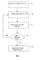
- FIG. 1a illustrates an exemplary sequence for forming a dielectric stack in accordance with a preferred embodiment.
- the sequence is shown for transistor gate dielectric structures between a semiconductor substrate and a gate electrode.
- the semiconductor substrate can be treated for subsequential ALD deposition (11).
- Such a treatment can comprise water, alcohol or Ozone treatment, intended to create surface -OH groups as known to a person skilled in the art.
- a first high-k dielectric layer is deposited on the semiconductor substrate by ALD (12).
- a dielectric layer is deposited on the first high-k layer by PECVD (13).
- the dielectric layer comprises at least Si and N. This can be done in the same tool, but in different reaction chambers. This sequence of two steps can be repeated n times (14).
- a transistor gate electrode is deposited over the dielectric layer (15).
- a step of post deposition anneal can be performed before depositing the gate electrode layer to further improve the film integrity, to promote intermixing of individual components in the stack, and to further optimize oxygen-to-nitrogen ratio in the film stack.
- Figure 1b illustrates another exemplary sequence for forming a dielectric stack in accordance with a preferred embodiment.
- the sequence is shown for transistor gate dielectric structures between a semiconductor substrate and a gate electrode.
- the semiconductor substrate can be treated for subsequential ALD deposition (11), as known by a person skilled in the art.
- a first high-k dielectric layer is deposited on the semiconductor substrate by ALD (12).
- a dielectric layer is deposited on the first high-k layer by PEALCVD (13).
- This step (13) comprises subjecting the substrate with the high-k dielectric layer to subsequent pulses of nitrogen comprising vapor phase reactants and silicon comprising vapor phase reactants.
- the dielectric layer comprises at least Si and N. This can be done in the same tool, but in different reaction chambers.
- This sequence of two steps can be repeated n times (14).
- a transistor gate electrode is deposited over the dielectric layer (15).
- a step of post deposition anneal can be performed before depositing the gate electrode layer to further improve the film integrity, to promote intermixing of individual components in the stack, and to further optimize oxygen-to-nitrogen ratio in the film stack.
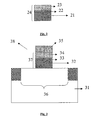
- a dielectric stack for an integrated circuit is disclosed.
- the dielectric stack is part of a transistor gate electrode structure.
- Figure 2 depicts a cross section of such a structure.
- the dielectric stack (24) comprises a high-k dielectric layer (21) comprising at least a high-k material, a dielectric layer (23) comprising at least silicon and nitrogen and an intermediate layer (22) between the high-k dielectric layer and the dielectric layer, the intermediate layer comprising the high-k dielectric material, silicon and nitrogen.
- the dielectric stack (24) can be repeated n times.
- a dielectric layer can be deposited between the substrate and the high-k dielectric layer.
- This layer can have the same characteristics as the dielectric layer discussed above.
- the crystallization temperature of the dielectric stack is higher than the crystallization temperature of the high-k dielectric layer.
- the crystallization temperature is higher than 600 degrees C, higher than 700 degrees C, preferably higher than 800 degrees C and more preferably higher than 900 degrees C.
- the crystallization temperature is between 800 degrees C and 1200 degrees C, between 800 degrees C and 1100 degrees C, and preferably between 900 degrees C and 1000 degrees C.
- the silicon and nitrogen comprising dielectric layer provides a maximum barrier to prevent interfacial reaction between the high-k dielectric layer and the conductive layer (e.g. polysilicon gate electrode) compared to any dielectric stack consisting of a high-k dielectric layer such as HfO 2 , HfO x N y or HfSiON based single layer dielectric layer.
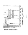
- Figure 3 illustrates an integrated circuit (IC) structure.
- the IC (38) is formed on a semiconductor substrate (31) above an active region (36).
- the IC comprises a dielectric stack (37) that replaces silicon dioxide dielectric layers as known in the prior art.
- the IC has a dielectric stack (37) being interposed between the gate electrode (35) and the upper surface of the active region (36).
- the dielectric stack consists of a high-k dielectric layer (32) comprising at least a high-k material, a dielectric layer (34) comprising at least silicon and nitrogen and an intermediate layer (33) between the high-k dielectric layer and the dielectric layer, the intermediate layer comprising the high-k material, silicon and nitrogen.
- the high-k material is preferably HfO 2 or ZrO 2
- the dielectric layer consists preferably of Si 3 N 4 or Si x O y N z
- the intermediate layer consists preferably of HfSiON produced by the plasma action in the PECVD or PEALCVD dielectric layer deposition process.
- This layer is preferably a mixture of the high-k material, silicon and nitrogen.
- This layer is preferably a mixture of the high-k material, silicon and nitrogen.
- the layers 32, 33 and 34 will repeat.
- the gate electrode (35) is polysilicon and more preferably polysilicon germanium.
- the thickness of the high-k dielectric layer is between 0.5 nm to 20 nm, between 0.5 nm and 10 nm, between 0.5 nm and 5 nm, between 0.5 nm and 1nm.
- the thickness of dielectric layer is between 0.5 to 20 nm, between 0.5 nm and 10 nm, between 0.5 nm and 5 nm, between 0.5 nm and 1nm.
- the thickness of he intermediate layer can be between 0.01 nm 2 nm, between 0.01 nm and 1 nm, between 0.01 nm and 0.5 nm.
- the present invention has the advantage that the incorporation of silicon and nitrogen into the high-k dielectric layer by forming an intermediate layer of metal-silicon oxynitride, leads to improved overall structural integrity and enhanced thermal stability.
- the present invention has further the advantage that the gate oxide thickness can be minimized without sacrificing the yield of the integrate circuits.
- the dielectric stack as provided in this invention leads to excellent equivalent oxide thickness (EOT), while maintaining leakage current reduction benefits from the high-k dielectric layer, which is beneficial since it allows scaling integrated circuits and transistors in particular.
- a method for forming a dielectric stack is formed.
- the dielectric stack comprises alternating layers of HfO 2 , SiN and an intermediate layer comprising Hf, Si and N.
- the method is disclosed in figure 4 .
- the method comprises the step of:
- This method results in the formation of a dielectric stack consisting of alternating layers of HfO 2 , SiN and an intermediate layer comprising Hf, Si and N.
- this dielectric stack will be referred to as the [HfO 2 /SiN]xZ laminate stack.
- Z refers to the number of times that the stack HfO 2 /SiN is repeated.
- hafnium dioxide HfO 2
- hafnium oxynitride HfO x N y
- Deposition of 1 st HfO 2 high-k layer is achieved by ALCVD which uses sequential exposure of the starting Si wafer surface to pulses of HfCl 4 and H 2 O precursors in a dedicated ALCVD reactor.
- ALCVD allows for precise HfO 2 thickness control down to (sub)monolayer level by self-limiting surface reactions during the HfCl 4 and H 2 O precursor exposure cycles, respectively.
- deposition of 1 st HfO x N y high-k dielectric is achieved by using sequential exposure of HfCl 4 , H 2 O and/or NH 3 precursors in a dedicated ALCVD reactor.
- the oxygen-to-nitrogen ratio in the ALCVD HfO x N y dielectric can be varied by controlling the H 2 O to NH 3 precursor cycle ratio after the prior HfCl 4 exposure cycle.
- the ALCVD layer produced is pure hafnium nitride, HfN.
- HfO 2 or HfO x N y include tetra-kis-diethylamido hafnium, TDEAH, Hf[N(C 2 H 5 ) 2 ] 4 and ozone (O 3 ).
- HfO 2 or HfO x N y thin dielectric layers are MOCVD or physical (sputter) deposition with suitable precursors or targets.
- an ultra-thin silicon (oxy)nitride cap or intermediate layer can be readily deposited, using a remote N 2 -plasma plus a dilute silane (SiH 4 ) flow in a PECVD reactor that is clustered with the ALCVD reactor. Silicon and nitrogen species are incorporated into the upper part of the underlying high-k dielectric layer in this process.
- the above CVD processes are repeated twice to complete the fabrication of the stack.
- a post deposition anneal step is performed to further improve the stack integrity and promote intermixing of material between the components.
- Final optimization of the dielectric stack composition in terms of nitrogen and oxygen content can be made by selecting either an oxidizing, nitridizing or inert ambient along with a suitable annealing temperature.
- Typical inert gas ambient includes N 2 , Ar, He.
- Typical oxidizing ambient gas includes O 2 , NO, N 2 O.
- Typical nitridizing gas ambient without oxygen is NH 3 .
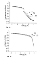
- Capacitor leakage experiments were performed for device structures obtained via the method described above.
- the gate electrode is a conducting polysilicon gate electrode. The results of the experiments are shown in figure 5 and 6 .
- the devices comprising a dielectric stack are achieved according to the following methods:
- 51 in figure 5 refers to devices with a 100 by 100 ⁇ m 2 device area
- 52 refers to devices with a 50 by 50 ⁇ m 2 device area
- 53 refers to devices with a 30 by 30 ⁇ m 2 device area.
- Experiment 5a shows low leakage current capacitor devices with well-behaved area-scaling.
- the effects of (a) silane and nitrogen plasma exposure; (b) silane exposure only; (c) N 2 -plasma exposure only and (d) N 2 post deposition anneal (PDA) on 4nm HfO 2 are shown.
- a thermal silane exposure without the N 2 -plasma ( Figure 5b ) on 4nm HfO 2 did not achieve the same low leakage current as in figure 5a .
- the plasma enhancement effect can be attributed to the enhanced reactivity of nitrogen-containing species produced by the plasma, either as ions or radicals.
- Figure 6a shows a TEM of a dielectric stack.
- the dielectric stack is obtained by the following method:
- 61 refers to the HfO 2 layer
- 62 refers to SiN layer
- 63 refer to the poly Si gate electrode.
- the dielectric stack was obtained by the method as described for figure 5a .
- Figure 6a shows that incorporation of silicon and nitrogen into bulk of the HfO 2 or HfO x N y high-k dielectric layers results in the formation of an intermediate layer of hafnium-silicon oxynitride (HfSiON), leading to improved overall structural integrity and enhanced thermal stability against interface reaction with polysilicon (gate electrode).
- the intermediate layer formation occurs due to the plasma action from the deposition of the silicon oxynitride by plasma enhanced chemical vapor deposition. Relative ratio of Hf, O, Si, and N components can be adjusted by individual layer thickness and deposition parameters.
- Figure 6b shows a TEM image of a dielectric stack obtained by the method /
- 61 refer to the HfO 2 layer
- 64 refer to a gray contrast haze layer
- 63 refers to the poly Si gate electrode.
- the silicon-rich SiN layer 62 of figure 6a between the HfO 2 layer and polisilicon gate electrode, provides an effective barrier to prevent undesired interfacial reaction between HfO 2 and polysilicon (gate electrode) compared to any HfO 2 , HfO x N y or HfSiON based single layer dielectric.
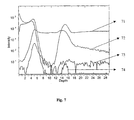
- the dielectric stacks are obtained by the method :
- HfN + secondary ions 71 refers in this figure to Si
- 72 refers to Hf
- 73 refers to SiN 2 , indicating the presence of an intermediate Hf(Si)-oxynitride layer between the HfO 2 layer and the SiN layer.
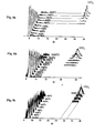
- Binary oxides such as ZrO 2 and HfO 2 have a crystallization onset temperature between 450-550 degrees C.
- the [HfO 2 /SiN] laminate approach significantly increases the crystallization onset temperature to 900-1000 degrees C.
- Figure 8a-c show the x-ray diffraction spectra of the [HfO 2 /SiN]x10 laminate structure with 30 ( figure 8a ), 20 ( figure 8b ) and 15 cycles ( figure 8c ) of HfCl 4 /H 2 O and 0.5nm SiN (repeated 10 times). Diffraction peaks located between 5-10 degrees 2-theta angle represent reflections from the individual laminated [HfO 2 /SiN] layers.
- the dielectric stacks were obtained according to the method:
- the dielectric stacks are obtained by the method of:
Landscapes
- Chemical & Material Sciences (AREA)
- Engineering & Computer Science (AREA)
- Metallurgy (AREA)
- Chemical Kinetics & Catalysis (AREA)
- Materials Engineering (AREA)
- Mechanical Engineering (AREA)
- General Chemical & Material Sciences (AREA)
- Organic Chemistry (AREA)
- Inorganic Chemistry (AREA)
- Physics & Mathematics (AREA)
- Electromagnetism (AREA)
- Plasma & Fusion (AREA)
- Insulated Gate Type Field-Effect Transistor (AREA)
- Formation Of Insulating Films (AREA)
- Semiconductor Memories (AREA)
Description
- The present invention as claimed in
claim 1 relates to integrated circuit fabrication processes and in particular to the formation of an integrated circuit comprising a multilayer dielectric stack of high-k material. The present invention as claimed inclaim 14 further relates to such dielectric stack in an integrated circuit and to a MOS transistor having such multilayer dielectric stack. Any reference to "invention" and "embodiment" is to be regarded as an example of implementation of the teachings herein unless said "invention" or "embodiment" is specifically claimed.
1Å = 0.1 nm ; 1 Torr = 133 Pa. - A multilayer dielectric stack according to the present invention replaces prior art silicon dioxide as dielectric layer in integrated circuits.
- When integrating a high-k dielectric with a gate electrode into a conventional CMOS gate stack, two major process/thermal stability issues need to be addressed and tackled. It is hereby important to
- 1. Reduce reaction(s) at the top interface between the high-k dielectric and the gate electrode such as polysilicon either during polysilicon deposition and/or during subsequent thermal processing and/or to
- 2. Minimize degradation of high-k material integrity due to crystallization, which leads to formation of structural defects such as oxygen vacancies and grain boundaries that interact with gate electrode deposition process leading to pathways of enhanced electrical leakage and/or of dopant/impurity diffusion.
- Based upon knowledge from conventional SiO2-based CMOS gate dielectric material (which is amorphous and 100% compatible with polysilicon gate), it is known that nitrogen is a key modifier introduced to improve the resistance against boron diffusion. Likewise, in high-k dielectric, enhanced stability against dopant (boron) diffusion from the polysilicon gate can be achieved through the use of a metal-oxynitride (MOxNy) or nitridation of metal oxide (
US patent No. 6,251,761 ).US 6,251,761 describes a gate stack including a gate dielectric with reduced effective electrical thickness. A high-k dielectric is deposited over the silicon substrate. In a next step, remote plasma nitridation of the high-k dielectric layer is performed to convert the upper surface of the high-k dielectric into a nitride layer. A conductive layer is formed over the nitride layer to complete the CMOS gate stack. - Published
US patent application No. 2002/0130340 A1 discloses a multilayer dielectric stack, which has alternating layers of high-k material and an interposing material. The interposing material can be Al2O3, AlN, SiN, Si3N4 and SiO2. The interposing material can be deposited by atomic layer deposition, sputtering or evaporation, resulting in the deposition of the interposing layer on the dielectric layer. Each layer is preferably less tan 50 Angstroms thick. This structure inhibits and prevents the crystallization of the high k-material. - Wu Y et al: "The performance and reliability of PMOSFET's with ultrathin silicon nitride/oxide stacked gate dielectrics with nitrided Si-Si02 interfaces prepared by remote plasma enhanced CVD and post-deposition rapid thermal annealing",IEEE Transactions on Electron Devices VOL. 47, No. 7, 1 July 2000, 1361-1369 teaches manufacture of a dielectric stack comprising SiO2/SiN with nitrided Si-Si02 interfaces prepared by PECVD.
- In a first aspect of this invention, a method for forming a dielectric stack in an integrated circuit structure is disclosed comprising the steps of:
- forming a high-k dielectric layer on a semiconductor substrate, and
- subjecting the semiconductor substrate with the high-k dielectric layer to a nitrogen comprising vapor phase reactant and a silicon comprising vapor phase reactant in a plasma-enhanced chemical vapor deposition process (PECVD) or plasma-enhanced atomic layer chemical vapor deposition (PE ALCVD) process.
- With a process according to the present invention, highly reactive species such as nitrogen ions or radicals and silicon species penetrate into the upper part of the high-k material, thereby promoting intermixing, densification and formation of an intermediate layer. The intermediate layer comprises at least the high-k material, silicon and nitrogen. Highly reactive species are formed by plasma-enhanced chemical vapor deposition (PECVD) or plasma-enhanced atomic layer chemical vapor deposition (PE ALCVD). Highly reactive species can be radicals or ions. Consequently, using PECVD or PE ALCVD, the species formed in the plasma penetrate into the upper part of the underlying high-k dielectric layer.
- The presence of both silicon and nitrogen contributes to the compatibility between the high-k dielectric layer and any other layer such as e.g. the gate electrode.
- Compared to prior art methods, the formation of an interfacial layer between the high-k dielectric layer and e.g. the gate electrode layer is avoided, thus leading to improved electrical properties.
- In an embodiment of the first aspect of this invention, a method as recited in any of the previous embodiments is disclosed wherein the subjecting step results in the formation of a dielectric layer comprising at least silicon and nitrogen and essentially no or no high-k material and in the formation of an intermediate layer disposed between the high-k dielectric layer and the dielectric layer, the intermediate layer comprising at least the high-k material, silicon and nitrogen.
- In a preferred embodiment, the dielectric layer is selected from the group consisting of SiN, SiON and Si3N4.
- In another embodiment of the first aspect of this invention, a method as recited in any of the previous embodiments is disclosed wherein the subjecting step results in the formation of an intermediate layer adjacent to the high-k dielectric layer and the dielectric layer, the intermediate layer comprising at least the high-k material, silicon and nitrogen. Preferably, the intermediate layer is on top of the high-k dielectric layer. The subjecting step results in essentially no and/or no formation at all of the dielectric layer (in the case of very thin layers).
- In an embodiment of the first aspect of this invention, a method as recited in any of the previous embodiments is disclosed further comprising subjecting the substrate with the high-k dielectric layer to an oxygen comprising vapor phase reactant. In this case, the intermediate layer formed comprises oxygen in addition.
- In a preferred embodiment, the silicon comprising compound or vapor phase reactant is selected from the group consisting of SiH4, Si2H6, Si3H8, SixHyClz and combinations thereof. In another preferred embodiment, the nitrogen comprising compound is selected from the group consisting of nitrogen, ammonia, N2H4, NO, N2O, and combinations thereof. In a further embodiment of the first aspect of this invention, a method as recited in any of the previous embodiments is disclosed wherein the ratio of silane:nitrogen containing compounds is in the range of 1:1 to 1:10000. Preferably, the ratio is between 1:1 and 1:1000.
- In an embodiment of the first aspect of this invention, a method as recited in any of the previous embodiments is disclosed further comprising repeating the forming step and the subjecting step between 2 and 100 times, between 2 and 50 times, between 10 and 50 times, between 10 and 30 times and between 2 and 10 times.
- In an embodiment of the first aspect of this invention, a method as recited in any of the previous embodiments is disclosed wherein the high-k dielectric layer comprises a high-k material selected from the group consisting of a transition metal or lanthanide oxide and a transition metal or lanthanide oxynitride. In a preferred embodiment, the high-k material is selected from the group consisting of ZrO2, HfO2, TiO2, Ta2O5, Al2O3, HfOxNy, HfN, LaxOy, LaAlO3, and/or mixtures thereof.
- In a preferred embodiment of the invention, the forming step comprises subjecting the semiconducting substrate to an atomic layer deposition process.
- In a preferred embodiment, the high-k material is selected from the group consisting of HfO2, HfOxNy and HfN.
- In an embodiment of the first aspect of this invention, a method as recited in any of the previous embodiments is disclosed wherein the subjecting step is performed in a plasma-enhanced chemical vapor deposition (PECVD) chamber at a temperature in the range of 300 to 600 degrees Celsius.
- In a further embodiment of the first aspect of this invention, a method as recited in any of the previous embodiments is disclosed wherein the subjecting step is performed in a plasma-enhanced atomic layer chemical vapor deposition chamber at a temperature in the range of 300 to 600 degrees Celsius. The semiconductor substrate with the high-k dielectric layer is subjected to alternating pulses of precursor compounds, the precursor compound being a nitrogen containing vapor phase reactant or a silicon containing vapor phase reactant.
- In a further embodiment of the first aspect of this invention, a method as recited in any of the previous embodiments is disclosed wherein the subjecting step is performed at a pressure in the range of 10-3 to 100 Torr. The pressure can vary, depending on the composition of reactants. For N2 as reactant, the pressure is preferably between 0.01 and 100 Torr, while for a silane reactant, the pressure is between 1 and 100 mTorr.
- In a further embodiment of the first aspect of this invention, a method as recited in any of the previous embodiments is disclosed wherein the subjecting step is performed in a plasma with a plasma density in the range of 1010 to 1013 reactive species cm-3.
- In another embodiment of the first aspect of this invention, a method as recited in any of the previous embodiments is disclosed wherein the high-k dielectric layer has a thickness in the range of 0.01 nm to 20 nm, 0.05 nm to 20 nm, 0.1 nm to 20 nm, 0.3 nm to 20 nm, 0.5 nm to 20 nm. The dielectric layer has a thickness in the range of 0.01 nm to 20 nm, 0.05 nm to 20 nm, 0.1 nm to 20 nm, 0.3 nm to 20 nm, 0.5 nm to 20 nm. Preferably, the thickness is below 1 nm, below 0.5 nm and below 0.3 nm. According to an embodiment of the first aspect of this invention, the dielectric layer has a thickness between 0.01 nm and 1 nm, between 0.01 nm and 0.5 nm, between 0.01 nm and 0.1 nm.
- In another embodiment of the first aspect of this invention, a method as recited in any of the previous embodiments is disclosed wherein the step of forming a high-k dielectric layer on a semiconductor substrate is performed by an atomic layer deposition process (ALD). In another embodiment of the first aspect of this invention, a method as recited in any of the previous embodiments is disclosed further comprising the step of annealing the semiconductor substrate at a temperature between 500 and 1000 degrees Celsius. Preferably, the substrate is annealed at a temperature between 600 and 900 degrees Celsius. The step of annealing can be performed after each individual step or can be performed after the formation of the dielectric stack.
- The method as recited in the previous embodiments can further comprise the step of depositing a conductive layer over the dielectric stack. The conductive layer can comprise silicon. The conductive layer can be polysilicon, polysilicon germanium or a metal. In a subsequent step, the dielectric stack and the electrode layer are patterned to form the desired integrated circuit.
- In a second aspect of the invention, a dielectric stack in an integrated circuit is provided. The dielectric stack comprises:
- a high-k dielectric layer comprising at least a high-k material; and
- an intermediate layer disposed between the high-k dielectric layer and the dielectric layer, the intermediate layer comprising the high-k material, silicon and nitrogen.
- In a preferred embodiment of the second aspect of this invention, a device a recited in any of the previous embodiments is disclosed wherein the dielectric stack further comprises a dielectric layer comprising at least silicon and nitrogen.
- In an embodiment of the second aspect of this invention, a device as recited in any of the previous embodiments is disclosed wherein the dielectric stack is characterized by a crystallization temperature, the crystallization temperature of the dielectric stack is higher than the crystallization temperature of the high-k material.
- In a preferred embodiment of the second aspect of this invention, a dielectric stack as recited in any of the previous embodiments is disclosed wherein the crystallization temperature is between 800 degrees C and 1200 degrees C.
- In another embodiment of the second aspect of this invention, the intermediate layer and the dielectric layer are formed by subjecting the semiconductor substrate with the high-k dielectric layer to a nitrogen comprising vapor phase reactant and a silicon comprising vapor phase reactant in a plasma-enhanced chemical vapor deposition process (PECVD) or plasma-enhanced atomic layer chemical vapor deposition (PE ALCVD) process.
- In another embodiment of the second aspect of this invention, the high-k layer is formed by subjecting the semiconductor substrate to an atomic layer deposition process.
- In another embodiment of the second aspect of this invention, a dielectric stack as recited in any of the previous embodiments is disclosed wherein a sequence of the high-k dielectric layer, the intermediate layer and the dielectric layer is repeated between 3 and 60 times. In a preferred embodiment, a dielectric stack is provided wherein between one of the high-k dielectric layers and an adjacent one of the dielectric layers an intermediate layer is disposed, the intermediate layer comprising the dielectric material, silicon and nitrogen.
- In another embodiment, the dielectric layer and the intermediate layer further comprise oxygen.
- In another embodiment of the second aspect of this invention, a dielectric stack as recited in any of the previous embodiments is disclosed wherein the dielectric layer does essentially not comprise the high-k material. In a preferred embodiment, the intermediate layer comprises the high-k material, nitrogen and silicon and optionally oxygen. In another embodiment, the stack as recited in any of the previous embodiments comprises a dielectric layer selected from the group consisting of SiN, SiON, and Si3N4.
In another embodiment of the second aspect of this invention, a dielectric stack as recited in any of the previous embodiments is disclosed wherein the high-k dielectric layer comprises a compound selected from the group consisting of a transition metal oxide or a transition metal oxynitride. In a preferred embodiment, the high-k dielectric layer comprises a high-k dielectric material selected from the group consisting of ZrO2, HfO2, TiO2, Ta2O5, Al2O3, HfOxNy, HfN and/or mixtures thereof. More preferably, the high-k dielectric material is selected from the group consisting of HfO2, HfOxNy and HfN. - In a further embodiment of the second aspect of this invention, a dielectric stack as recited in any of the previous embodiment is disclosed wherein the high-k dielectric layer has a thickness between 0.5 nm to 20 nm.
- In a further embodiment of the second aspect of this invention, a dielectric stack as recited in any of the previous embodiment is disclosed wherein the dielectric layer has a thickness in the range of 0.01 nm to 20 nm, 0.05 nm to 20 nm, 0.1 nm to 20 nm, 0.3 nm to 20 nm, 0.5 nm to 20 nm. Preferably, the thickness is below 1 nm, below 0.5 nm and below 0.3 nm. According to an embodiment of the second aspect of this invention, the dielectric layer has a thickness between 0.01 nm and 1 nm, between 0.01 nm and 0.5 nm, between 0.01 nm and 0.1 nm.
- In an embodiment of the invention, the intermediate layer comprises Hf, nitrogen and silicon and oxygen.
- Preferably the dielectric layer of the stack is selected from the group consisting of SiN, SiON and Si3N4.
- In a third aspect of this invention, a MOS transistor is disclosed. The MOS transistor comprises:
- a gate electrode;
- a channel region having an upper surface underlying the gate electrode; and
- a dielectric stack being interposed between the gate electrode and the upper surface of the channel region, the dielectric stack comprising a high-k dielectric layer comprising at least a high-k material, a dielectric layer comprising at least silicon and nitrogen and an intermediate layer between the high-k dielectric layer and the dielectric layer, the intermediate layer comprising the high-k material, silicon and nitrogen.
- The dielectric stack is characterized by the features as disclosed in the second aspect of the invention.
-
- The
figure 1a represents a flow chart of a method of forming a dielectric stack according to a preferred embodiment of the invention. - The
figure 1b represents a flow chart of a method of forming a dielectric stack according to another preferred embodiment of the invention. - The
figure 2 represents a schematic view of a dielectric stack according to an embodiment of the present invention. - The
figure 3 represents a schematic view of an integrated circuit structure according to an embodiment of the present invention. - The
figure 4 represents a flow chart of a method of forming an integrated circuit according to a preferred embodiment of the invention. - The
figures 5a-d represent the results of capacitor leakage experiments for devices obtained according to various methods. - The
figures 6a-b represents a TEM picture of dielectric stacks obtained according to various methods. - The
figure 7 represents a ToF-SIMS depth profile for a preferred embodiment of a device of the present invention. - The
figures 8a-c represents X-Ray diffraction spectra of devices obtained according to various methods. - The
figure 9 represents channel electron mobility measurements from n-MOSFET devices obtained according to various methods. - The
figure 10 represents the cumulative distribution of gate leakage current for 30 diode/capacitor devices obtained according to different methods. - In relation to the appended drawings the present invention is described in details in the sequel. It is apparent however that a person skilled in the art can imagine several other equivalent embodiments or other ways of executing the present invention.
- While the invention is described in conjunction with a MOS transistor, it will be apparent to those ordinary skilled in the art that the benefits of this invention can be applied to other transistor structures and other structures such as memory cell capacitors. In particular, one ordinary skilled in the art can imagine other situations where similar electrical and physical properties at an interface are desired.
- For the purpose of this invention, a Plasma enhanced CVD or plasma enhanced ALCVD process should be understood as a process wherein at least one chemical compound is subjected to a plasma source, thereby creating highly reactive species such as radicals or ions.
- The term high-k dielectric layer should be understood as a layer comprising a high-k material. A high-k material is a dielectric material having a dielectric constant greater than the dielectric constant of silicon oxide and preferably greater than 10.
- The high-k material can be a high-k material selected from the group consisting of a transition metal oxide or a transition metal oxynitride, a rare earth metal oxide, a rare earth metal oxynitride. Transition metals can be Group IV or Group V metals such as e.g. Ti, Zr, Hf, V, Nb, and Ta. Rare earth metal can be Lanthanides such as e.g. So, Ce, Pr, Eu. Lanthanides meaning an element from the lanthanide series. High-k material can also include lanthanum oxide, neodymium oxide and cerium oxide. Preferably, the metal is Hafnium (Hf). Preferably, the high-k material is selected from the group consisting of ZrO2, HfO2, TiO2, Ta2O5, Al2O3, HfOxNy, HfN and/or mixtures thereof. Preferably, the high-k material is LaAlO3, ZrO2 or HfO2, more preferably ZrO2 or HfO2, more preferably HfO2.
- In a first aspect of this invention, a method for forming a dielectric stack is provided, the method comprising the steps of:
- forming a high-k dielectric layer on a semiconductor substrate, and
- subjecting the semiconductor substrate to nitrogen comprising vapor phase reactants and silicon comprising vapor phase reactants in a plasma-enhanced chemical vapor deposition process (PECVD) or plasma-enhanced atomic layer chemical vapor deposition (PE ALCVD) process.
- Preferably, the forming step and the subjecting step are repeated n times, such that a laminate structure is formed n can be between 2 and 100, between 3 and 70, between 3 and 60, between 3 and 50, between 3 and 40, between 2 and 30, between 2 and 20, between 2 and 10.
- The method can further comprise the step of depositing a gate electrode adjacent to the dielectric layer. Preferably, the gate electrode will be deposited on top of the dielectric layer. The gate electrode can be a conducting or semiconducting material such as poly Si or poly SiGe (polysilicon germanium).
- The high-k dielectric layer can be formed by ALD, ALCVD, MOCVD (metalorganic chemical vapor deposition) or sputtering.
- The plasma enhancement effect can be attributed to the enhanced reactivity of nitrogen containing species produced by the plasma, either as ions or as radicals. Energy released from ion bombardment or by radicals help to promote intermixing, densification and incorporation of silicon and nitrogen into the high-k dielectric layer. The presence of both silicon and nitrogen contributes to the compatibility between the high-k dielectric layer and the gate electrode.
- The dielectric layer between the high-k dielectric layer and gate electrode contributes to minimize interfacial reactions between polysilicon and high-k dielectric layer at elevated temperature.
-
Figure 1a illustrates an exemplary sequence for forming a dielectric stack in accordance with a preferred embodiment. The sequence is shown for transistor gate dielectric structures between a semiconductor substrate and a gate electrode. Initially, the semiconductor substrate can be treated for subsequential ALD deposition (11). Such a treatment can comprise water, alcohol or Ozone treatment, intended to create surface -OH groups as known to a person skilled in the art. Subsequently, a first high-k dielectric layer is deposited on the semiconductor substrate by ALD (12). A dielectric layer is deposited on the first high-k layer by PECVD (13). The dielectric layer comprises at least Si and N. This can be done in the same tool, but in different reaction chambers. This sequence of two steps can be repeated n times (14). Subsequently, a transistor gate electrode is deposited over the dielectric layer (15). - Optionally, a step of post deposition anneal can be performed before depositing the gate electrode layer to further improve the film integrity, to promote intermixing of individual components in the stack, and to further optimize oxygen-to-nitrogen ratio in the film stack.
-
Figure 1b illustrates another exemplary sequence for forming a dielectric stack in accordance with a preferred embodiment. The sequence is shown for transistor gate dielectric structures between a semiconductor substrate and a gate electrode. Initially, the semiconductor substrate can be treated for subsequential ALD deposition (11), as known by a person skilled in the art. Subsequently, a first high-k dielectric layer is deposited on the semiconductor substrate by ALD (12). A dielectric layer is deposited on the first high-k layer by PEALCVD (13). This step (13) comprises subjecting the substrate with the high-k dielectric layer to subsequent pulses of nitrogen comprising vapor phase reactants and silicon comprising vapor phase reactants. The dielectric layer comprises at least Si and N. This can be done in the same tool, but in different reaction chambers. This sequence of two steps can be repeated n times (14). Subsequently, a transistor gate electrode is deposited over the dielectric layer (15). - Optionally, a step of post deposition anneal can be performed before depositing the gate electrode layer to further improve the film integrity, to promote intermixing of individual components in the stack, and to further optimize oxygen-to-nitrogen ratio in the film stack.
- In a second aspect of this invention a dielectric stack for an integrated circuit is disclosed. In an embodiment, the dielectric stack is part of a transistor gate electrode structure.
Figure 2 depicts a cross section of such a structure. The dielectric stack (24) comprises a high-k dielectric layer (21) comprising at least a high-k material, a dielectric layer (23) comprising at least silicon and nitrogen and an intermediate layer (22) between the high-k dielectric layer and the dielectric layer, the intermediate layer comprising the high-k dielectric material, silicon and nitrogen. The dielectric stack (24) can be repeated n times. - Optionally, a dielectric layer can be deposited between the substrate and the high-k dielectric layer. This layer can have the same characteristics as the dielectric layer discussed above.
- The crystallization temperature of the dielectric stack is higher than the crystallization temperature of the high-k dielectric layer. The crystallization temperature is higher than 600 degrees C, higher than 700 degrees C, preferably higher than 800 degrees C and more preferably higher than 900 degrees C. The crystallization temperature is between 800 degrees C and 1200 degrees C, between 800 degrees C and 1100 degrees C, and preferably between 900 degrees C and 1000 degrees C.
- The silicon and nitrogen comprising dielectric layer provides a maximum barrier to prevent interfacial reaction between the high-k dielectric layer and the conductive layer (e.g. polysilicon gate electrode) compared to any dielectric stack consisting of a high-k dielectric layer such as HfO2, HfOxNy or HfSiON based single layer dielectric layer.
-
Figure 3 illustrates an integrated circuit (IC) structure. The IC (38) is formed on a semiconductor substrate (31) above an active region (36). The IC comprises a dielectric stack (37) that replaces silicon dioxide dielectric layers as known in the prior art. The IC has a dielectric stack (37) being interposed between the gate electrode (35) and the upper surface of the active region (36). The dielectric stack consists of a high-k dielectric layer (32) comprising at least a high-k material, a dielectric layer (34) comprising at least silicon and nitrogen and an intermediate layer (33) between the high-k dielectric layer and the dielectric layer, the intermediate layer comprising the high-k material, silicon and nitrogen. - The high-k material is preferably HfO2 or ZrO2, while the dielectric layer consists preferably of Si3N4 or SixOyNz. The intermediate layer consists preferably of HfSiON produced by the plasma action in the PECVD or PEALCVD dielectric layer deposition process. This layer is preferably a mixture of the high-k material, silicon and nitrogen. This layer is preferably a mixture of the high-k material, silicon and nitrogen.
- In a preferred embodiment, the
layers - In a preferred embodiment, the gate electrode (35) is polysilicon and more preferably polysilicon germanium.
- The thickness of the high-k dielectric layer is between 0.5 nm to 20 nm, between 0.5 nm and 10 nm, between 0.5 nm and 5 nm, between 0.5 nm and 1nm. The thickness of dielectric layer is between 0.5 to 20 nm, between 0.5 nm and 10 nm, between 0.5 nm and 5 nm, between 0.5 nm and 1nm. The thickness of he intermediate layer can be between 0.01
nm 2 nm, between 0.01 nm and 1 nm, between 0.01 nm and 0.5 nm. - The present invention has the advantage that the incorporation of silicon and nitrogen into the high-k dielectric layer by forming an intermediate layer of metal-silicon oxynitride, leads to improved overall structural integrity and enhanced thermal stability.
- The present invention has further the advantage that the gate oxide thickness can be minimized without sacrificing the yield of the integrate circuits. The dielectric stack as provided in this invention leads to excellent equivalent oxide thickness (EOT), while maintaining leakage current reduction benefits from the high-k dielectric layer, which is beneficial since it allows scaling integrated circuits and transistors in particular.
- In a preferred embodiment, a method for forming a dielectric stack is formed. The dielectric stack comprises alternating layers of HfO2, SiN and an intermediate layer comprising Hf, Si and N. The method is disclosed in
figure 4 . The method comprises the step of: - preparing a silicon surface for ALD (41);
- forming a layer of HfO2 by atomic layer chemical vapor deposition (ALCVD) on the silicon substrate (42);
- subjecting the silicon substrate with the HfO2 layer to a nitrogen containing species and a silicon containing species in a plasma enhanced chemical vapor deposition process (PECVD) (43),repeating step (42) and (43) n times, n being an integer between 0 and 100. Preferably, n is between 2 and 100, between 3 and 70, between 3 and 60, between 3 and 50, between 3 and 40, between 3 and 30, or between 2 and 10; and then
- depositing a poly Si gate electrode layer (45).
- This method results in the formation of a dielectric stack consisting of alternating layers of HfO2, SiN and an intermediate layer comprising Hf, Si and N. For the purpose of this invention, this dielectric stack will be referred to as the [HfO2/SiN]xZ laminate stack. Z refers to the number of times that the stack HfO2/SiN is repeated. This dielectric stack results in advantages obtained by 1) incorporation of silicon and nitrogen into the high-k material; 2) formation of an intermediate layer containing HfSiON. Consequently, high-k/polysilicon interface reaction is prevented and concurrently the thermal stability of the high-k material against crystallization is improved.
- Deposition of 1st HfO2 high-k layer is achieved by ALCVD which uses sequential exposure of the starting Si wafer surface to pulses of HfCl4 and H2O precursors in a dedicated ALCVD reactor. ALCVD allows for precise HfO2 thickness control down to (sub)monolayer level by self-limiting surface reactions during the HfCl4 and H2O precursor exposure cycles, respectively.
- Alternatively, deposition of 1st HfOxNy high-k dielectric is achieved by using sequential exposure of HfCl4, H2O and/or NH3 precursors in a dedicated ALCVD reactor. The oxygen-to-nitrogen ratio in the ALCVD HfOxNy dielectric can be varied by controlling the H2O to NH3 precursor cycle ratio after the prior HfCl4 exposure cycle. In the case of using NH3 precursor only, the ALCVD layer produced is pure hafnium nitride, HfN. Other precursors that can be used for producing HfO2 or HfOxNy include tetra-kis-diethylamido hafnium, TDEAH, Hf[N(C2H5)2]4 and ozone (O3).
- Alternative methods to produce HfO2 or HfOxNy thin dielectric layers are MOCVD or physical (sputter) deposition with suitable precursors or targets.
- Following the formation of HfO2 high-k dielectric, an ultra-thin silicon (oxy)nitride cap or intermediate layer can be readily deposited, using a remote N2-plasma plus a dilute silane (SiH4) flow in a PECVD reactor that is clustered with the ALCVD reactor. Silicon and nitrogen species are incorporated into the upper part of the underlying high-k dielectric layer in this process.
The above CVD processes are repeated twice to complete the fabrication of the stack. - A post deposition anneal step is performed to further improve the stack integrity and promote intermixing of material between the components. Final optimization of the dielectric stack composition in terms of nitrogen and oxygen content can be made by selecting either an oxidizing, nitridizing or inert ambient along with a suitable annealing temperature. Typical inert gas ambient includes N2, Ar, He. Typical oxidizing ambient gas includes O2, NO, N2O. Typical nitridizing gas ambient without oxygen is NH3.
- Capacitor leakage experiments were performed for device structures obtained via the method described above. The gate electrode is a conducting polysilicon gate electrode. The results of the experiments are shown in
figure 5 and6 . - The devices comprising a dielectric stack are achieved according to the following methods:
-
- treating Si substrate to a mixture of O3 and DI water to obtain an -OH terminated surface,
- subjecting Si substrate subsequently to HfCl4 and H2O precursors (one cycle) in ALD chamber, repeat this up to a total of 80 cycles, resulting in a layer of HfO2 of approximate thickness of 4 nm,
- subjecting Si substrate with HfO2 layer to a mixture of silane + MRG (microwave radical generator) N2 plasma at 600 degrees C for 15 seconds in a PECVD chamber,
- deposition of the poly silicon gate layer, and
- post gate electrode anneal at 1000 degrees C.
-
- treating Si substrate to a mixture of O3 and DI water to obtain an -OH terminated surface,
- subjecting Si substrate subsequently to HfCl4 and H2O precursors (one cycle) in ALD chamber, repeat this up to a total of 80 cycles, resulting in a layer of HfO2 of approximate thickness of 4 nm,
- subjecting Si substrate with HfO2 layer to silane without N2 plasma at 600 degrees C for 15 seconds,
- deposition of the poly silicon gate layer, and
- post gate electrode anneal at 1000 degrees C.
-
- treating Si substrate to a mixture of O3 and DI water to obtain an -OH terminated surface,
- subjecting Si substrate subsequently to HfCl4 and H2O precursors (one cycle) in ALD chamber, repeat this up to a total of 80 cycles, resulting in a layer of HfO2 of approximate thickness of 4 nm,
- subjecting Si substrate with HfO2 layer to MRG N2 plasma in a PECVD chamber at 600 degrees C for 15 seconds,
- deposition of the poly silicon gate layer, and
- post gate electrode anneal at 1000 degrees C
-
- treating Si substrate to a mixture of O3 and DI water to obtain an -OH terminated surface,
- subjecting Si substrate subsequently to HfCl4 and H2O precursors (one cycle) in ALD chamber, repeat this up to a total of 80 cycles, resulting in a layer of HfO2 of approximate thickness of 4 nm,
- subjecting Si substrate with HfO2 layer to N2
- post deposition anneal (PDA) treatment at 600 degrees C for 15 seconds,
- deposition of the poly silicon gate layer, and
- post gate electrode anneal at 1000 degrees C
- 51 in
figure 5 refers to devices with a 100 by 100 µm2 device area, 52 refers to devices with a 50 by 50 µm2 device area, 53 refers to devices with a 30 by 30 µm2 device area. - Experiment 5a shows low leakage current capacitor devices with well-behaved area-scaling. In the next set of comparison experiments, the effects of (a) silane and nitrogen plasma exposure; (b) silane exposure only; (c) N2-plasma exposure only and (d) N2 post deposition anneal (PDA) on 4nm HfO2 are shown. A thermal silane exposure without the N2-plasma (
Figure 5b ) on 4nm HfO2 did not achieve the same low leakage current as infigure 5a . The plasma enhancement effect can be attributed to the enhanced reactivity of nitrogen-containing species produced by the plasma, either as ions or radicals. Energy released from ion bombardment or by radicals help to promote intermixing, densification and silicon/nitrogen incorporation into the HfO2 high-k dielectric. The presence of both silicon and nitrogen contributes to ensure polysilicon compatibility of the 4nm HfO2 dielectric as a N2-plasma treatment alone (Figure 5c ) or a N2 post deposition anneal treatment (Figure 5d ) did not achieve the same low leakage current as the plasma CVD SiN-HfO2 control (Figure 5a ). Thus, the incorporation of silicon and nitrogen into the HfO2 from the N2-plasma/silane plasma by plasma enhanced CVD process deposition process contributes to a dielectric stack with desired chemical composition and structural/electrical integrity. - The effect of reduced interface reaction between polysilicon gate and high-k material is demonstrated in the cross-sectional TEM images shown in
Figure 6. Figure 6a shows a TEM of a dielectric stack. The dielectric stack is obtained by the following method: - treating Si substrate to a mixture of O3 and DI water to obtain an -OH terminated surface,
- subjecting Si substrate subsequently to HfCl4 and H2O precursors (one cycle) in ALD chamber, repeat this up to a total of 80 cycles, resulting in a layer of HfO2 of approximate thickness of 4 nm,
- subjecting Si substrate with HfO2 layer to a mixture of silane + MRG (microwave radical generator) N2 plasma at 600 degrees C for 15 seconds in a PECVD chamber,
- deposition of the poly silicon gate layer, and
- post gate electrode anneal at 1000 degrees C.
- In
figure 6a , 61 refers to the HfO2 layer, 62 refers to SiN layer and 63 refer to the poly Si gate electrode. The dielectric stack was obtained by the method as described forfigure 5a .Figure 6a shows that incorporation of silicon and nitrogen into bulk of the HfO2 or HfOxNy high-k dielectric layers results in the formation of an intermediate layer of hafnium-silicon oxynitride (HfSiON), leading to improved overall structural integrity and enhanced thermal stability against interface reaction with polysilicon (gate electrode). The intermediate layer formation occurs due to the plasma action from the deposition of the silicon oxynitride by plasma enhanced chemical vapor deposition. Relative ratio of Hf, O, Si, and N components can be adjusted by individual layer thickness and deposition parameters. -
Figure 6b shows a TEM image of a dielectric stack obtained by the method / - treating Si substrate to a mixture of O3 and DI water to obtain an -OH terminated surface,
- subjecting Si substrate subsequently to HfCl4 and H2O precursors (one cycle) in ALD chamber, repeat this up to a total of 80 cycles, resulting in a layer of HfO2 of approximate thickness of 4 nm,
- deposition of the poly silicon gate layer, and
- post gate electrode anneal at 1000 degrees C.
- In
figure 6b , 61 refer to the HfO2 layer, 64 refer to a gray contrast haze layer, and typical for the HfO2/polySi interface due to interface reaction and 63 refers to the poly Si gate electrode. - The silicon-
rich SiN layer 62 offigure 6a , between the HfO2 layer and polisilicon gate electrode, provides an effective barrier to prevent undesired interfacial reaction between HfO2 and polysilicon (gate electrode) compared to any HfO2, HfOxNy or HfSiON based single layer dielectric. - An example of the intermixing of the high-k layer with silicon and nitrogen is described in the ToF SIMS depth profiles shown in
Figure 7 . - The dielectric stacks are obtained by the method :
- treating Si substrate to a mixture of O3 and DI water to obtain an -OH terminated surface,
- subjecting Si substrate subsequently to HfCl4 and H2O precursors (one cycle) in ALD chamber, repeat this up to a total of 80 cycles, resulting in a layer of HfO2 of approximate thickness of 4 nm,
- subjecting Si substrate with HfO2 layer to a mixture of silane + MRG (microwave radical generator) N2 plasma for 150 seconds in a PECVD chamber at 600 degrees C, resulting in a layer of SiN (thickness approximately 5nm),
- deposition of the poly silicon gate layer, and
- post gate electrode anneal at 1000 degrees C.
- ToF-SIMS depth profiles show the presence of HfN+ secondary ions (74). 71 refers in this figure to Si, 72 refers to Hf and 73 refers to SiN2, indicating the presence of an intermediate Hf(Si)-oxynitride layer between the HfO2 layer and the SiN layer.
- Experimental results on crystallization temperature of the dielectric stack are shown in
figure 8 . - Binary oxides such as ZrO2 and HfO2 have a crystallization onset temperature between 450-550 degrees C. The [HfO2/SiN] laminate approach significantly increases the crystallization onset temperature to 900-1000 degrees C.
Figure 8a-c show the x-ray diffraction spectra of the [HfO2/SiN]x10 laminate structure with 30 (figure 8a ), 20 (figure 8b ) and 15 cycles (figure 8c ) of HfCl4/H2O and 0.5nm SiN (repeated 10 times). Diffraction peaks located between 5-10 degrees 2-theta angle represent reflections from the individual laminated [HfO2/SiN] layers. As a function of increasing annealing temperature, a second x-ray diffraction peak located between 2-theta angle of 29-31 degrees start to emerge at or above 900°C, indicating the crystallization of the HfO2 phase-separated from [HfO2/SiN] laminate. - The dielectric stacks were obtained according to the method:
- treating Si substrate to a mixture of O3 and DI water to obtain an -OH terminated surface,
- performing 10 times the sequence of steps :
- subjecting Si substrate subsequently to HfCl4 and H2O precursors (one cycle) in ALD chamber, repeat this up to a total of y cycles, resulting in layer of HfO2, and
- subjecting Si substrate with HfO2 layer to a mixture of silane + MRG (microwave radical generator) N2 plasma in a PECVD chamber at 550 degrees C, resulting in a layer of SiN.
- Hereby, y=30 (
figure 8a ), y=20 (figure 8b ), y=15 (figure 8c ). -
Figure 9 shows channel electron mobility measurements from nMOSFET devices fabricated with HfO2 (91), HfO2/SiN (92), and [HfO2/SiN]x2 (z=2) laminate (93) as dielectric stack. It can be seen that the [HfO2/SiN]x2 laminate (93) and the HfO2/SiN (92) has a higher peak and overall mobility compared to the HfO2 reference (91). - The dielectric stacks are obtained by the method of:
- treating Si substrate to a mixture of O3 and DI water to obtain an -OH terminated surface,
- subjecting Si substrate subsequently to HfCl4 and H2O precursors (one cycle) in ALD chamber, (up to a total of 80 cycles for
condition 91, 60 cycles forcondition - subjecting Si substrate with HfO2 layer to a mixture of silane + MRG (microwave radical generator) N2 plasma in a PECVD chamber at 550 degrees C, resulting in a layer of SiN deposition of the poly silicon gate layer (only for
condition 92 and 93), and optionally - repeating both subjecting steps once (only for condition 93).
-
Figure 10 show the cumulative distribution of gate leakage current for a sample of 30 diode/capacitor devices. The devices are obtained according to method described above (conditions figure 9 ). Both the HfO2/SiN and [HfO2/SiN]x2 (z=2) devices give near 100% yield whereas about 30% HfO2 devices fail the leakage distribution trend.
Claims (25)
- A method for fabricating a dielectric stack in an integrated circuit comprising the steps of :- forming a high-k dielectric layer on a semiconductor substrate, and- subjecting said semiconductor substrate with said high-k dielectric layer to a nitrogen comprising vapor phase reactant and a silicon comprising vapor phase reactant in a plasma-enhanced chemical vapor deposition process (PECVD) or a plasma-enhanced atomic layer chemical vapor deposition (PE ALCVD) process, resulting in the formation of at least an intermediate layer comprising at least the high-k material, silicon and nitrogen and in the formation of a dielectric layer comprising at least silicon and nitrogen and no high-k material and wherein said intermediate layer is disposed between said high-k dielectric layer and said dielectric layer wherein said high-k dielectric layer comprises a high-k material selected from the group consisting of ZrO2, HfO2, TiO2, Ta2O5, Al2O3, HfOxNy, HfN and mixtures thereof.
- The method according to claim 1 wherein the method further comprises subjecting said substrate with said high-k dielectric layer to an oxygen comprising vapor phase reactant.
- The method according to any of the previous claims further comprising repeating said forming step and said subjecting step between 2 and 50 times.
- The method according to any of the previous claims wherein said forming step comprises subjecting the semiconducting substrate to an atomic layer deposition process.
- The method according to any of the previous claims wherein said subjecting step is performed in a plasma-enhanced chemical vapor deposition (PECVD) chamber at a temperature in the range of 300 to 600 degrees Celsius.
- The method according to any of the previous claims wherein said subjecting step is performed in a plasma-enhanced atomic layer chemical vapor deposition chamber at a temperature in the range of 300 to 600 degrees Celsius.
- The method according to any of the previous claims wherein said subjecting step is performed at a pressure in the range of 10-3 to 100 Torr.
- The method according to any of the previous claims wherein said subjecting step is performed in a plasma with a plasma density in the range of 1010 to 1013 cm-3.
- The method according to any of the previous claims wherein said silicon comprising vapor phase reactant is selected from the group consisting of SiH4, Si2H6, Si3H8, SixHyClz and combinations thereof.
- The method according to any of the previous claims wherein said nitrogen comprising vapor phase reactant is selected from the group consisting of nitrogen, ammonia, N2H4, NO, N2O, and combinations thereof.
- The method according to any of the previous claims wherein said high-k dielectric layer has a thickness in the range of 0.5 nm to 20 nm.
- The method according to any of the previous claims wherein said dielectric layer has a thickness in the range of 0.5 to 20 nm.
- The method according to any of the previous claims further comprising the step of depositing a conductive layer over the dielectric stack.
- A dielectric stack in an integrated circuit comprising :- a high-k dielectric layer comprising at least a high-k material, wherein the high-k dielectric layer is overlying a semiconductor substrate;- a dielectric layer comprising at least silicon and nitrogen and not comprising said high-k material; and- an intermediate layer disposed between said high-k dielectric layer and said dielectric layer, said intermediate layer comprising said high-k material, silicon and nitrogenwherein the intermediate layer is on top of the high-k dielectric layer and said high-k dielectric layer comprises a high-k material selected from the group consisting of ZrO2, HfO2, TiO2, Ta2O5, Al2O3, HfOxNy, HfN and mixtures thereof.
- The dielectric stack according to claim 14 wherein the crystallization temperature of said dielectric stack is higher than the crystallization temperature of the high-k material.
- The dielectric stack according to any of claims 14 or 15 wherein the crystallization temperature of said dielectric stack is between 800 degrees Celsius and 1200 degrees Celsius.
- The dielectric stack according to any of claims 14 to 16 wherein a sequence of said high-k dielectric layer, said intermediate layer and said dielectric layer is repeated between 3 and 60 times.
- The dielectric stack according to claim 17 wherein between one of said high-k dielectric layers and an adjacent one of said dielectric layers an intermediate layer is disposed, said intermediate layer comprising at least said dielectric material, silicon and nitrogen.
- The dielectric stack according to any of claims 14 to 18 wherein said dielectric layer further comprises oxygen.
- The dielectric stack according to any of claims 14 to 19 wherein said high-k dielectric layer has a thickness between 0.5 nm to 20 nm.
- The dielectric stack according to any of claims 14 to 20 wherein said dielectric layer has a thickness in the range of 0.5 to 20 nm.
- The dielectric stack according to any of claims 14 to 21 wherein said intermediate layer comprises Hf, nitrogen and silicon and oxygen.
- The dielectric stack according to any of claims 14 to 22 wherein said dielectric layer is selected from the group consisting of SiN, SiON and Si3N4.
- The dielectric stack according to any of claims 14 to 23 wherein said high-k dielectric layer is formed by an atomic layer deposition process.
- A MOS transistor comprising:- a gate electrode;- a channel region having an upper surface underlying the gate electrode; and- a dielectric stack according to any of the claims 14 to 24 being interposed between the gate electrode and the upper surface of the channel region,wherein the gate electrode is over the dielectric layer of the dielectric stack.
Applications Claiming Priority (3)
| Application Number | Priority Date | Filing Date | Title |
|---|---|---|---|
| US43182402P | 2002-12-09 | 2002-12-09 | |
| US431824P | 2002-12-09 | ||
| PCT/BE2003/000213 WO2004053997A1 (en) | 2002-12-09 | 2003-12-09 | Method for forming a dielectric stack |
Publications (2)
| Publication Number | Publication Date |
|---|---|
| EP1570525A1 EP1570525A1 (en) | 2005-09-07 |
| EP1570525B1 true EP1570525B1 (en) | 2015-12-02 |
Family
ID=32507800
Family Applications (1)
| Application Number | Title | Priority Date | Filing Date |
|---|---|---|---|
| EP03782011.5A Expired - Lifetime EP1570525B1 (en) | 2002-12-09 | 2003-12-09 | Method for forming a dielectric stack |
Country Status (5)
| Country | Link |
|---|---|
| US (2) | US7465626B2 (en) |
| EP (1) | EP1570525B1 (en) |
| JP (2) | JP4647311B2 (en) |
| AU (1) | AU2003289764A1 (en) |
| WO (1) | WO2004053997A1 (en) |
Families Citing this family (39)
| Publication number | Priority date | Publication date | Assignee | Title |
|---|---|---|---|---|
| JP4681886B2 (en) | 2003-01-17 | 2011-05-11 | 富士通セミコンダクター株式会社 | Semiconductor device |
| US20040144980A1 (en) * | 2003-01-27 | 2004-07-29 | Ahn Kie Y. | Atomic layer deposition of metal oxynitride layers as gate dielectrics and semiconductor device structures utilizing metal oxynitride layers |
| US7514360B2 (en) * | 2004-03-17 | 2009-04-07 | Hong Yu Yu | Thermal robust semiconductor device using HfN as metal gate electrode and the manufacturing process thereof |
| US20050224897A1 (en) * | 2004-03-26 | 2005-10-13 | Taiwan Semiconductor Manufacturing Co., Ltd. | High-K gate dielectric stack with buffer layer to improve threshold voltage characteristics |
| KR100539213B1 (en) * | 2004-07-10 | 2005-12-27 | 삼성전자주식회사 | Method of forming a composite dielectric layer and method of manufacturing a semiconductor device using the same |
| US7595538B2 (en) * | 2004-08-17 | 2009-09-29 | Nec Electronics Corporation | Semiconductor device |
| US7507629B2 (en) * | 2004-09-10 | 2009-03-24 | Gerald Lucovsky | Semiconductor devices having an interfacial dielectric layer and related methods |
| JP4309320B2 (en) * | 2004-09-13 | 2009-08-05 | 株式会社東芝 | Semiconductor device and manufacturing method thereof |
| JP4966490B2 (en) * | 2004-11-15 | 2012-07-04 | 富士通セミコンダクター株式会社 | Manufacturing method of semiconductor device |
| US7235501B2 (en) | 2004-12-13 | 2007-06-26 | Micron Technology, Inc. | Lanthanum hafnium oxide dielectrics |
| JP2006190801A (en) * | 2005-01-06 | 2006-07-20 | Fujitsu Ltd | Film-forming method and semiconductor device manufacturing method |
| US7365027B2 (en) * | 2005-03-29 | 2008-04-29 | Micron Technology, Inc. | ALD of amorphous lanthanide doped TiOx films |
| JP2006324363A (en) * | 2005-05-17 | 2006-11-30 | Elpida Memory Inc | Capacitor and manufacturing method thereof |
| US20060267113A1 (en) * | 2005-05-27 | 2006-11-30 | Tobin Philip J | Semiconductor device structure and method therefor |
| KR100780661B1 (en) * | 2005-06-29 | 2007-11-29 | 주식회사 하이닉스반도체 | Dielectric Film of Nonvolatile Memory Device and Formation Method |
| KR100706784B1 (en) * | 2005-08-08 | 2007-04-12 | 삼성전자주식회사 | Semiconductor device and manufacturing method thereof. |
| US7436034B2 (en) * | 2005-12-19 | 2008-10-14 | International Business Machines Corporation | Metal oxynitride as a pFET material |
| US7524727B2 (en) | 2005-12-30 | 2009-04-28 | Intel Corporation | Gate electrode having a capping layer |
| US8097300B2 (en) | 2006-03-31 | 2012-01-17 | Tokyo Electron Limited | Method of forming mixed rare earth oxynitride and aluminum oxynitride films by atomic layer deposition |
| US7759746B2 (en) | 2006-03-31 | 2010-07-20 | Tokyo Electron Limited | Semiconductor device with gate dielectric containing aluminum and mixed rare earth elements |
| US8012442B2 (en) | 2006-03-31 | 2011-09-06 | Tokyo Electron Limited | Method of forming mixed rare earth nitride and aluminum nitride films by atomic layer deposition |
| US7767262B2 (en) | 2006-09-29 | 2010-08-03 | Tokyo Electron Limited | Nitrogen profile engineering in nitrided high dielectric constant films |
| KR20080046438A (en) * | 2006-11-22 | 2008-05-27 | 삼성전자주식회사 | Semiconductor device and manufacturing method thereof |
| KR100877100B1 (en) * | 2007-04-16 | 2009-01-09 | 주식회사 하이닉스반도체 | Nonvolatile Memory Device Manufacturing Method |
| KR100909967B1 (en) * | 2007-06-08 | 2009-07-29 | 삼성전자주식회사 | Manufacturing method of semiconductor device |
| US20090047796A1 (en) * | 2007-08-13 | 2009-02-19 | Taiwan Semiconductor Manufacturing Co., Ltd. | Method of Manufacturing a Dielectric Layer having Plural High-K Films |
| US8633074B2 (en) | 2008-09-17 | 2014-01-21 | Spansion Llc | Electrically programmable and erasable memory device and method of fabrication thereof |
| KR20100086853A (en) * | 2009-01-23 | 2010-08-02 | 삼성전자주식회사 | Method of fabricating phase change memory device having tic layer |
| JP5247619B2 (en) * | 2009-07-28 | 2013-07-24 | キヤノンアネルバ株式会社 | Dielectric film, semiconductor device manufacturing method using the dielectric film, and semiconductor manufacturing apparatus |
| US8076241B2 (en) | 2009-09-30 | 2011-12-13 | Tokyo Electron Limited | Methods for multi-step copper plating on a continuous ruthenium film in recessed features |
| US8541275B2 (en) * | 2009-11-12 | 2013-09-24 | International Business Machines Corporation | Single metal gate CMOS integration by intermixing polarity specific capping layers |
| US8987095B2 (en) * | 2011-08-19 | 2015-03-24 | Taiwan Semiconductor Manufacturing Company, Ltd. | Method of fabricating a carbon-free dielectric layer over a carbon-doped dielectric layer |
| US9006094B2 (en) | 2012-04-18 | 2015-04-14 | International Business Machines Corporation | Stratified gate dielectric stack for gate dielectric leakage reduction |
| US20140023794A1 (en) * | 2012-07-23 | 2014-01-23 | Maitreyee Mahajani | Method And Apparatus For Low Temperature ALD Deposition |
| US8981466B2 (en) | 2013-03-11 | 2015-03-17 | International Business Machines Corporation | Multilayer dielectric structures for semiconductor nano-devices |
| US9553160B2 (en) * | 2013-10-09 | 2017-01-24 | Taiwan Semiconductor Manufacturing Co., Ltd. | Mechanisms for monitoring impurity in high-K dielectric film |
| US10121655B2 (en) | 2015-11-20 | 2018-11-06 | Applied Materials, Inc. | Lateral plasma/radical source |
| WO2018101278A1 (en) * | 2016-11-30 | 2018-06-07 | 株式会社リコー | Coating liquid for forming oxide or oxynitride insulator film, oxide or oxynitride insulator film, field effect transistor, and methods for manufacturing these |
| FI129628B (en) * | 2019-09-25 | 2022-05-31 | Beneq Oy | Method and apparatus for machining a substrate surface |
Citations (1)
| Publication number | Priority date | Publication date | Assignee | Title |
|---|---|---|---|---|
| EP0834489A1 (en) * | 1996-10-04 | 1998-04-08 | Dow Corning Corporation | Thick opaque ceramic coatings |
Family Cites Families (18)
| Publication number | Priority date | Publication date | Assignee | Title |
|---|---|---|---|---|
| JPS6338248A (en) * | 1986-08-04 | 1988-02-18 | Hitachi Ltd | Semiconductor device and manufacture thereof |
| JP2764472B2 (en) * | 1991-03-25 | 1998-06-11 | 東京エレクトロン株式会社 | Semiconductor film formation method |
| JP3180404B2 (en) * | 1992-01-10 | 2001-06-25 | ソニー株式会社 | Method of forming capacitive element |
| JP3529989B2 (en) * | 1997-09-12 | 2004-05-24 | 株式会社東芝 | Film forming method and semiconductor device manufacturing method |
| US6251761B1 (en) | 1998-11-24 | 2001-06-26 | Texas Instruments Incorporated | Process for polycrystalline silicon gates and high-K dielectric compatibility |
| US20020024139A1 (en) * | 2000-02-04 | 2002-02-28 | Chan Simon S. | Combined capping layer and ARC for CU interconnects |
| US6407435B1 (en) * | 2000-02-11 | 2002-06-18 | Sharp Laboratories Of America, Inc. | Multilayer dielectric stack and method |
| DE10010286A1 (en) * | 2000-02-25 | 2001-09-13 | Infineon Technologies Ag | Method for filling depressions in a surface of a semiconductor structure and a semiconductor structure filled in this way |
| US6287897B1 (en) * | 2000-02-29 | 2001-09-11 | International Business Machines Corporation | Gate dielectric with self forming diffusion barrier |
| US6984591B1 (en) * | 2000-04-20 | 2006-01-10 | International Business Machines Corporation | Precursor source mixtures |
| US6638877B2 (en) * | 2000-11-03 | 2003-10-28 | Texas Instruments Incorporated | Ultra-thin SiO2using N2O as the oxidant |
| US20020142531A1 (en) * | 2001-03-29 | 2002-10-03 | Hsu Sheng Teng | Dual damascene copper gate and interconnect therefore |
| US6867101B1 (en) * | 2001-04-04 | 2005-03-15 | Advanced Micro Devices, Inc. | Method of fabricating a semiconductor device having a nitride/high-k/nitride gate dielectric stack by atomic layer deposition (ALD) and a device thereby formed |
| US6573197B2 (en) * | 2001-04-12 | 2003-06-03 | International Business Machines Corporation | Thermally stable poly-Si/high dielectric constant material interfaces |
| US6528430B2 (en) * | 2001-05-01 | 2003-03-04 | Samsung Electronics Co., Ltd. | Method of forming silicon containing thin films by atomic layer deposition utilizing Si2C16 and NH3 |
| US6656282B2 (en) * | 2001-10-11 | 2003-12-02 | Moohan Co., Ltd. | Atomic layer deposition apparatus and process using remote plasma |
| US6645882B1 (en) * | 2002-01-17 | 2003-11-11 | Advanced Micro Devices, Inc. | Preparation of composite high-K/standard-K dielectrics for semiconductor devices |
| US6642573B1 (en) * | 2002-03-13 | 2003-11-04 | Advanced Micro Devices, Inc. | Use of high-K dielectric material in modified ONO structure for semiconductor devices |
-
2003
- 2003-12-09 EP EP03782011.5A patent/EP1570525B1/en not_active Expired - Lifetime
- 2003-12-09 JP JP2004557681A patent/JP4647311B2/en not_active Expired - Lifetime
- 2003-12-09 WO PCT/BE2003/000213 patent/WO2004053997A1/en not_active Ceased
- 2003-12-09 AU AU2003289764A patent/AU2003289764A1/en not_active Abandoned
-
2005
- 2005-05-25 US US11/138,746 patent/US7465626B2/en not_active Expired - Lifetime
-
2008
- 2008-11-17 US US12/272,614 patent/US20090079016A1/en not_active Abandoned
-
2010
- 2010-06-16 JP JP2010137515A patent/JP5214667B2/en not_active Expired - Lifetime
Patent Citations (1)
| Publication number | Priority date | Publication date | Assignee | Title |
|---|---|---|---|---|
| EP0834489A1 (en) * | 1996-10-04 | 1998-04-08 | Dow Corning Corporation | Thick opaque ceramic coatings |
Non-Patent Citations (1)
| Title |
|---|
| WU Y ET AL: "THE PERFORMANCE AND RELIABILITY OF PMOSFET'S WITH ULTRATHIN SILICON NITRIDE/OXIDE STACKED GATE DIELECTRICS WITH NITRIDED SI-SIO2 INTERFACES PREPARED BY REMOTE PLASMA ENHANCED CVD AND POST-DEPOSITION RAPID THERMAL ANNEALING", IEEE TRANSACTIONS ON ELECTRON DEVICES, IEEE SERVICE CENTER, PISACATAWAY, NJ, US, vol. 47, no. 7, 1 July 2000 (2000-07-01), pages 1361 - 1369, XP000958477, ISSN: 0018-9383, DOI: 10.1109/16.848278 * |
Also Published As
| Publication number | Publication date |
|---|---|
| US7465626B2 (en) | 2008-12-16 |
| EP1570525A1 (en) | 2005-09-07 |
| US20090079016A1 (en) | 2009-03-26 |
| JP4647311B2 (en) | 2011-03-09 |
| JP2010245548A (en) | 2010-10-28 |
| AU2003289764A8 (en) | 2004-06-30 |
| AU2003289764A1 (en) | 2004-06-30 |
| WO2004053997A1 (en) | 2004-06-24 |
| JP2006511934A (en) | 2006-04-06 |
| JP5214667B2 (en) | 2013-06-19 |
| US20050269651A1 (en) | 2005-12-08 |
Similar Documents
| Publication | Publication Date | Title |
|---|---|---|
| EP1570525B1 (en) | Method for forming a dielectric stack | |
| CN1832143B (en) | High dielectric constant material | |
| US7135361B2 (en) | Method for fabricating transistor gate structures and gate dielectrics thereof | |
| US6809370B1 (en) | High-k gate dielectric with uniform nitrogen profile and methods for making the same | |
| US6020243A (en) | Zirconium and/or hafnium silicon-oxynitride gate dielectric | |
| KR100568448B1 (en) | Manufacturing method of high dielectric film with reduced impurities | |
| US20050285208A1 (en) | Metal gate electrode for semiconductor devices | |
| KR101052587B1 (en) | Dielectric Films and Semiconductor Devices Using Dielectric Films | |
| US20040106261A1 (en) | Method of forming an electrode with adjusted work function | |
| US20080268653A1 (en) | Method of forming high dielectric film using atomic layer deposition and method of manufacturing capacitor having the high dielectric film | |
| JP2003059926A (en) | Semiconductor device | |
| WO2004008827A2 (en) | Atomic layer deposition of high k dielectric films | |
| US20090008725A1 (en) | Method for deposition of an ultra-thin electropositive metal-containing cap layer | |
| WO2003058695A1 (en) | Preparation of stack high-k gate dielectrics with nitrided layer | |
| EP1649501B1 (en) | High-k dielectric film, method of forming the same and related semiconductor device | |
| US7601578B2 (en) | Defect control in gate dielectrics | |
| WO2009133515A1 (en) | Gate structure for field effect transistor | |
| Wilk et al. | Improved film growth and flatband voltage control of ALD HfO/sub 2/and Hf-Al-O with n/sup+/poly-Si gates using chemical oxides and optimized post-annealing | |
| US7704821B2 (en) | In-situ nitridation of high-k dielectrics | |
| US7303970B2 (en) | Method of fabricating dielectric mixed layers and capacitive element and use thereof | |
| Swerts et al. | Highly scalable ALD-deposited hafnium silicate gate stacks for low standby power applications | |
| KR20050061077A (en) | Method for forming dielectric layer in semiconductor device | |
| Heyns et al. | High-k dielectric materials prepared by Atomic Layer CVD |
Legal Events
| Date | Code | Title | Description |
|---|---|---|---|
| PUAI | Public reference made under article 153(3) epc to a published international application that has entered the european phase |
Free format text: ORIGINAL CODE: 0009012 |
|
| 17P | Request for examination filed |
Effective date: 20050621 |
|
| AK | Designated contracting states |
Kind code of ref document: A1 Designated state(s): AT BE BG CH CY CZ DE DK EE ES FI FR GB GR HU IE IT LI LU MC NL PT RO SE SI SK TR |
|
| AX | Request for extension of the european patent |
Extension state: AL LT LV MK |
|
| DAX | Request for extension of the european patent (deleted) | ||
| 17Q | First examination report despatched |
Effective date: 20080915 |
|
| RAP1 | Party data changed (applicant data changed or rights of an application transferred) |
Owner name: ASM AMERICA, INC. Owner name: IMEC |
|
| REG | Reference to a national code |
Ref country code: DE Ref legal event code: R079 Ref document number: 60348313 Country of ref document: DE Free format text: PREVIOUS MAIN CLASS: H01L0029430000 Ipc: H01L0021316000 |
|
| GRAP | Despatch of communication of intention to grant a patent |
Free format text: ORIGINAL CODE: EPIDOSNIGR1 |
|
| RIC1 | Information provided on ipc code assigned before grant |
Ipc: H01L 21/316 20060101AFI20150519BHEP Ipc: H01L 29/43 20060101ALI20150519BHEP Ipc: H01L 21/314 20060101ALI20150519BHEP Ipc: H01L 29/49 20060101ALI20150519BHEP Ipc: H01L 21/318 20060101ALI20150519BHEP Ipc: H01L 29/51 20060101ALI20150519BHEP |
|
| INTG | Intention to grant announced |
Effective date: 20150622 |
|
| GRAS | Grant fee paid |
Free format text: ORIGINAL CODE: EPIDOSNIGR3 |
|
| GRAA | (expected) grant |
Free format text: ORIGINAL CODE: 0009210 |
|
| AK | Designated contracting states |
Kind code of ref document: B1 Designated state(s): AT BE BG CH CY CZ DE DK EE ES FI FR GB GR HU IE IT LI LU MC NL PT RO SE SI SK TR |
|
| REG | Reference to a national code |
Ref country code: GB Ref legal event code: FG4D |
|
| REG | Reference to a national code |
Ref country code: AT Ref legal event code: REF Ref document number: 763962 Country of ref document: AT Kind code of ref document: T Effective date: 20151215 Ref country code: CH Ref legal event code: EP |
|
| REG | Reference to a national code |
Ref country code: IE Ref legal event code: FG4D |
|
| REG | Reference to a national code |
Ref country code: DE Ref legal event code: R096 Ref document number: 60348313 Country of ref document: DE |
|
| REG | Reference to a national code |
Ref country code: FR Ref legal event code: PLFP Year of fee payment: 13 |
|
| REG | Reference to a national code |
Ref country code: NL Ref legal event code: MP Effective date: 20160302 |
|
| REG | Reference to a national code |
Ref country code: AT Ref legal event code: MK05 Ref document number: 763962 Country of ref document: AT Kind code of ref document: T Effective date: 20151202 |
|
| PG25 | Lapsed in a contracting state [announced via postgrant information from national office to epo] |
Ref country code: ES Free format text: LAPSE BECAUSE OF FAILURE TO SUBMIT A TRANSLATION OF THE DESCRIPTION OR TO PAY THE FEE WITHIN THE PRESCRIBED TIME-LIMIT Effective date: 20151202 |
|
| PG25 | Lapsed in a contracting state [announced via postgrant information from national office to epo] |
Ref country code: AT Free format text: LAPSE BECAUSE OF FAILURE TO SUBMIT A TRANSLATION OF THE DESCRIPTION OR TO PAY THE FEE WITHIN THE PRESCRIBED TIME-LIMIT Effective date: 20151202 Ref country code: BE Free format text: LAPSE BECAUSE OF NON-PAYMENT OF DUE FEES Effective date: 20151231 Ref country code: SE Free format text: LAPSE BECAUSE OF FAILURE TO SUBMIT A TRANSLATION OF THE DESCRIPTION OR TO PAY THE FEE WITHIN THE PRESCRIBED TIME-LIMIT Effective date: 20151202 Ref country code: FI Free format text: LAPSE BECAUSE OF FAILURE TO SUBMIT A TRANSLATION OF THE DESCRIPTION OR TO PAY THE FEE WITHIN THE PRESCRIBED TIME-LIMIT Effective date: 20151202 Ref country code: NL Free format text: LAPSE BECAUSE OF FAILURE TO SUBMIT A TRANSLATION OF THE DESCRIPTION OR TO PAY THE FEE WITHIN THE PRESCRIBED TIME-LIMIT Effective date: 20151202 Ref country code: GR Free format text: LAPSE BECAUSE OF FAILURE TO SUBMIT A TRANSLATION OF THE DESCRIPTION OR TO PAY THE FEE WITHIN THE PRESCRIBED TIME-LIMIT Effective date: 20160303 |
|
| PG25 | Lapsed in a contracting state [announced via postgrant information from national office to epo] |
Ref country code: IT Free format text: LAPSE BECAUSE OF FAILURE TO SUBMIT A TRANSLATION OF THE DESCRIPTION OR TO PAY THE FEE WITHIN THE PRESCRIBED TIME-LIMIT Effective date: 20151202 Ref country code: CZ Free format text: LAPSE BECAUSE OF FAILURE TO SUBMIT A TRANSLATION OF THE DESCRIPTION OR TO PAY THE FEE WITHIN THE PRESCRIBED TIME-LIMIT Effective date: 20151202 |
|
| REG | Reference to a national code |
Ref country code: CH Ref legal event code: PL |
|
| PG25 | Lapsed in a contracting state [announced via postgrant information from national office to epo] |
Ref country code: PT Free format text: LAPSE BECAUSE OF FAILURE TO SUBMIT A TRANSLATION OF THE DESCRIPTION OR TO PAY THE FEE WITHIN THE PRESCRIBED TIME-LIMIT Effective date: 20160404 Ref country code: SK Free format text: LAPSE BECAUSE OF FAILURE TO SUBMIT A TRANSLATION OF THE DESCRIPTION OR TO PAY THE FEE WITHIN THE PRESCRIBED TIME-LIMIT Effective date: 20151202 Ref country code: EE Free format text: LAPSE BECAUSE OF FAILURE TO SUBMIT A TRANSLATION OF THE DESCRIPTION OR TO PAY THE FEE WITHIN THE PRESCRIBED TIME-LIMIT Effective date: 20151202 Ref country code: RO Free format text: LAPSE BECAUSE OF FAILURE TO SUBMIT A TRANSLATION OF THE DESCRIPTION OR TO PAY THE FEE WITHIN THE PRESCRIBED TIME-LIMIT Effective date: 20151202 |
|
| REG | Reference to a national code |
Ref country code: DE Ref legal event code: R097 Ref document number: 60348313 Country of ref document: DE |
|
| REG | Reference to a national code |
Ref country code: IE Ref legal event code: MM4A |
|
| PG25 | Lapsed in a contracting state [announced via postgrant information from national office to epo] |
Ref country code: MC Free format text: LAPSE BECAUSE OF FAILURE TO SUBMIT A TRANSLATION OF THE DESCRIPTION OR TO PAY THE FEE WITHIN THE PRESCRIBED TIME-LIMIT Effective date: 20151202 |
|
| PLBE | No opposition filed within time limit |
Free format text: ORIGINAL CODE: 0009261 |
|
| STAA | Information on the status of an ep patent application or granted ep patent |
Free format text: STATUS: NO OPPOSITION FILED WITHIN TIME LIMIT |
|
| PG25 | Lapsed in a contracting state [announced via postgrant information from national office to epo] |
Ref country code: CH Free format text: LAPSE BECAUSE OF NON-PAYMENT OF DUE FEES Effective date: 20151231 Ref country code: LI Free format text: LAPSE BECAUSE OF NON-PAYMENT OF DUE FEES Effective date: 20151231 Ref country code: DK Free format text: LAPSE BECAUSE OF FAILURE TO SUBMIT A TRANSLATION OF THE DESCRIPTION OR TO PAY THE FEE WITHIN THE PRESCRIBED TIME-LIMIT Effective date: 20151202 Ref country code: IE Free format text: LAPSE BECAUSE OF NON-PAYMENT OF DUE FEES Effective date: 20151209 |
|
| 26N | No opposition filed |
Effective date: 20160905 |
|
| REG | Reference to a national code |
Ref country code: FR Ref legal event code: PLFP Year of fee payment: 14 |
|
| GBPC | Gb: european patent ceased through non-payment of renewal fee |
Effective date: 20160302 |
|
| PG25 | Lapsed in a contracting state [announced via postgrant information from national office to epo] |
Ref country code: SI Free format text: LAPSE BECAUSE OF FAILURE TO SUBMIT A TRANSLATION OF THE DESCRIPTION OR TO PAY THE FEE WITHIN THE PRESCRIBED TIME-LIMIT Effective date: 20151202 |
|
| PG25 | Lapsed in a contracting state [announced via postgrant information from national office to epo] |
Ref country code: BE Free format text: LAPSE BECAUSE OF FAILURE TO SUBMIT A TRANSLATION OF THE DESCRIPTION OR TO PAY THE FEE WITHIN THE PRESCRIBED TIME-LIMIT Effective date: 20151202 |
|
| PG25 | Lapsed in a contracting state [announced via postgrant information from national office to epo] |
Ref country code: GB Free format text: LAPSE BECAUSE OF NON-PAYMENT OF DUE FEES Effective date: 20160302 |
|
| PG25 | Lapsed in a contracting state [announced via postgrant information from national office to epo] |
Ref country code: HU Free format text: LAPSE BECAUSE OF FAILURE TO SUBMIT A TRANSLATION OF THE DESCRIPTION OR TO PAY THE FEE WITHIN THE PRESCRIBED TIME-LIMIT; INVALID AB INITIO Effective date: 20031209 Ref country code: BG Free format text: LAPSE BECAUSE OF FAILURE TO SUBMIT A TRANSLATION OF THE DESCRIPTION OR TO PAY THE FEE WITHIN THE PRESCRIBED TIME-LIMIT Effective date: 20151202 |
|
| PG25 | Lapsed in a contracting state [announced via postgrant information from national office to epo] |
Ref country code: CY Free format text: LAPSE BECAUSE OF FAILURE TO SUBMIT A TRANSLATION OF THE DESCRIPTION OR TO PAY THE FEE WITHIN THE PRESCRIBED TIME-LIMIT Effective date: 20151202 |
|
| PG25 | Lapsed in a contracting state [announced via postgrant information from national office to epo] |
Ref country code: TR Free format text: LAPSE BECAUSE OF FAILURE TO SUBMIT A TRANSLATION OF THE DESCRIPTION OR TO PAY THE FEE WITHIN THE PRESCRIBED TIME-LIMIT Effective date: 20151202 |
|
| REG | Reference to a national code |
Ref country code: FR Ref legal event code: PLFP Year of fee payment: 15 |
|
| PG25 | Lapsed in a contracting state [announced via postgrant information from national office to epo] |
Ref country code: LU Free format text: LAPSE BECAUSE OF NON-PAYMENT OF DUE FEES Effective date: 20151209 |
|
| PGFP | Annual fee paid to national office [announced via postgrant information from national office to epo] |
Ref country code: FR Payment date: 20221123 Year of fee payment: 20 Ref country code: DE Payment date: 20221122 Year of fee payment: 20 |
|
| REG | Reference to a national code |
Ref country code: DE Ref legal event code: R071 Ref document number: 60348313 Country of ref document: DE |