KR20120053784A - Light emitting diode chip having wavelength converting layer, method of fabricating the same and package having the same - Google Patents
Light emitting diode chip having wavelength converting layer, method of fabricating the same and package having the same Download PDFInfo
- Publication number
- KR20120053784A KR20120053784A KR1020100115082A KR20100115082A KR20120053784A KR 20120053784 A KR20120053784 A KR 20120053784A KR 1020100115082 A KR1020100115082 A KR 1020100115082A KR 20100115082 A KR20100115082 A KR 20100115082A KR 20120053784 A KR20120053784 A KR 20120053784A
- Authority
- KR
- South Korea
- Prior art keywords
- wavelength conversion
- layer
- light emitting
- emitting diode
- conversion layer
- Prior art date
Links
Images


Classifications
-
- H—ELECTRICITY
- H01—ELECTRIC ELEMENTS
- H01L—SEMICONDUCTOR DEVICES NOT COVERED BY CLASS H10
- H01L24/00—Arrangements for connecting or disconnecting semiconductor or solid-state bodies; Methods or apparatus related thereto
- H01L24/93—Batch processes
- H01L24/95—Batch processes at chip-level, i.e. with connecting carried out on a plurality of singulated devices, i.e. on diced chips
- H01L24/96—Batch processes at chip-level, i.e. with connecting carried out on a plurality of singulated devices, i.e. on diced chips the devices being encapsulated in a common layer, e.g. neo-wafer or pseudo-wafer, said common layer being separable into individual assemblies after connecting
-
- H—ELECTRICITY
- H01—ELECTRIC ELEMENTS
- H01L—SEMICONDUCTOR DEVICES NOT COVERED BY CLASS H10
- H01L21/00—Processes or apparatus adapted for the manufacture or treatment of semiconductor or solid state devices or of parts thereof
- H01L21/02—Manufacture or treatment of semiconductor devices or of parts thereof
- H01L21/02104—Forming layers
- H01L21/02365—Forming inorganic semiconducting materials on a substrate
- H01L21/02518—Deposited layers
- H01L21/02521—Materials
- H01L21/02538—Group 13/15 materials
- H01L21/0254—Nitrides
-
- H—ELECTRICITY
- H01—ELECTRIC ELEMENTS
- H01L—SEMICONDUCTOR DEVICES NOT COVERED BY CLASS H10
- H01L21/00—Processes or apparatus adapted for the manufacture or treatment of semiconductor or solid state devices or of parts thereof
- H01L21/70—Manufacture or treatment of devices consisting of a plurality of solid state components formed in or on a common substrate or of parts thereof; Manufacture of integrated circuit devices or of parts thereof
- H01L21/77—Manufacture or treatment of devices consisting of a plurality of solid state components or integrated circuits formed in, or on, a common substrate
- H01L21/78—Manufacture or treatment of devices consisting of a plurality of solid state components or integrated circuits formed in, or on, a common substrate with subsequent division of the substrate into plural individual devices
-
- H—ELECTRICITY
- H01—ELECTRIC ELEMENTS
- H01L—SEMICONDUCTOR DEVICES NOT COVERED BY CLASS H10
- H01L25/00—Assemblies consisting of a plurality of individual semiconductor or other solid state devices ; Multistep manufacturing processes thereof
- H01L25/03—Assemblies consisting of a plurality of individual semiconductor or other solid state devices ; Multistep manufacturing processes thereof all the devices being of a type provided for in the same subgroup of groups H01L27/00 - H01L33/00, or in a single subclass of H10K, H10N, e.g. assemblies of rectifier diodes
- H01L25/04—Assemblies consisting of a plurality of individual semiconductor or other solid state devices ; Multistep manufacturing processes thereof all the devices being of a type provided for in the same subgroup of groups H01L27/00 - H01L33/00, or in a single subclass of H10K, H10N, e.g. assemblies of rectifier diodes the devices not having separate containers
- H01L25/075—Assemblies consisting of a plurality of individual semiconductor or other solid state devices ; Multistep manufacturing processes thereof all the devices being of a type provided for in the same subgroup of groups H01L27/00 - H01L33/00, or in a single subclass of H10K, H10N, e.g. assemblies of rectifier diodes the devices not having separate containers the devices being of a type provided for in group H01L33/00
- H01L25/0753—Assemblies consisting of a plurality of individual semiconductor or other solid state devices ; Multistep manufacturing processes thereof all the devices being of a type provided for in the same subgroup of groups H01L27/00 - H01L33/00, or in a single subclass of H10K, H10N, e.g. assemblies of rectifier diodes the devices not having separate containers the devices being of a type provided for in group H01L33/00 the devices being arranged next to each other
-
- H—ELECTRICITY
- H01—ELECTRIC ELEMENTS
- H01L—SEMICONDUCTOR DEVICES NOT COVERED BY CLASS H10
- H01L33/00—Semiconductor devices with at least one potential-jump barrier or surface barrier specially adapted for light emission; Processes or apparatus specially adapted for the manufacture or treatment thereof or of parts thereof; Details thereof
- H01L33/02—Semiconductor devices with at least one potential-jump barrier or surface barrier specially adapted for light emission; Processes or apparatus specially adapted for the manufacture or treatment thereof or of parts thereof; Details thereof characterised by the semiconductor bodies
- H01L33/10—Semiconductor devices with at least one potential-jump barrier or surface barrier specially adapted for light emission; Processes or apparatus specially adapted for the manufacture or treatment thereof or of parts thereof; Details thereof characterised by the semiconductor bodies with a light reflecting structure, e.g. semiconductor Bragg reflector
-
- H—ELECTRICITY
- H01—ELECTRIC ELEMENTS
- H01L—SEMICONDUCTOR DEVICES NOT COVERED BY CLASS H10
- H01L33/00—Semiconductor devices with at least one potential-jump barrier or surface barrier specially adapted for light emission; Processes or apparatus specially adapted for the manufacture or treatment thereof or of parts thereof; Details thereof
- H01L33/36—Semiconductor devices with at least one potential-jump barrier or surface barrier specially adapted for light emission; Processes or apparatus specially adapted for the manufacture or treatment thereof or of parts thereof; Details thereof characterised by the electrodes
- H01L33/38—Semiconductor devices with at least one potential-jump barrier or surface barrier specially adapted for light emission; Processes or apparatus specially adapted for the manufacture or treatment thereof or of parts thereof; Details thereof characterised by the electrodes with a particular shape
- H01L33/382—Semiconductor devices with at least one potential-jump barrier or surface barrier specially adapted for light emission; Processes or apparatus specially adapted for the manufacture or treatment thereof or of parts thereof; Details thereof characterised by the electrodes with a particular shape the electrode extending partially in or entirely through the semiconductor body
-
- H—ELECTRICITY
- H01—ELECTRIC ELEMENTS
- H01L—SEMICONDUCTOR DEVICES NOT COVERED BY CLASS H10
- H01L33/00—Semiconductor devices with at least one potential-jump barrier or surface barrier specially adapted for light emission; Processes or apparatus specially adapted for the manufacture or treatment thereof or of parts thereof; Details thereof
- H01L33/48—Semiconductor devices with at least one potential-jump barrier or surface barrier specially adapted for light emission; Processes or apparatus specially adapted for the manufacture or treatment thereof or of parts thereof; Details thereof characterised by the semiconductor body packages
- H01L33/50—Wavelength conversion elements
-
- H—ELECTRICITY
- H01—ELECTRIC ELEMENTS
- H01L—SEMICONDUCTOR DEVICES NOT COVERED BY CLASS H10
- H01L2224/00—Indexing scheme for arrangements for connecting or disconnecting semiconductor or solid-state bodies and methods related thereto as covered by H01L24/00
- H01L2224/01—Means for bonding being attached to, or being formed on, the surface to be connected, e.g. chip-to-package, die-attach, "first-level" interconnects; Manufacturing methods related thereto
- H01L2224/42—Wire connectors; Manufacturing methods related thereto
- H01L2224/47—Structure, shape, material or disposition of the wire connectors after the connecting process
- H01L2224/48—Structure, shape, material or disposition of the wire connectors after the connecting process of an individual wire connector
- H01L2224/4805—Shape
- H01L2224/4809—Loop shape
- H01L2224/48091—Arched
-
- H—ELECTRICITY
- H01—ELECTRIC ELEMENTS
- H01L—SEMICONDUCTOR DEVICES NOT COVERED BY CLASS H10
- H01L2933/00—Details relating to devices covered by the group H01L33/00 but not provided for in its subgroups
- H01L2933/0008—Processes
- H01L2933/0033—Processes relating to semiconductor body packages
- H01L2933/0041—Processes relating to semiconductor body packages relating to wavelength conversion elements
Abstract
Description
본 발명은 발광 다이오드 칩, 그것을 제조하는 방법 및 그것을 갖는 패키지에 관한 것으로, 더욱 상세하게는 파장변환층을 갖는 발광 다이오드 칩, 그것을 제조하는 방법 및 그것을 갖는 패키지에 관한 것이다.The present invention relates to a light emitting diode chip, a method of manufacturing the same, and a package having the same, and more particularly, to a light emitting diode chip having a wavelength conversion layer, a method of manufacturing the same, and a package having the same.
현재 발광 다이오드는 경박단소화가 가능하고, 에너지 절감과 오랜 기간 동안 수명이 유지되는 장점으로 인해 휴대폰을 비롯한 각종 표시장치의 배면 광원으로 이용되고 있으며, 발광 다이오드를 실장한 발광소자, 즉 발광 다이오드 패키지는 높은 연색성을 갖는 백색광 구현이 가능하기 때문에 형광등과 같은 백색광원을 대체하여 일반조명에도 적용될 것으로 기대되고 있다.Currently, light emitting diodes are used as a light source for rear display of various display devices including mobile phones due to light and small size, energy saving, and long life. Since white light having high color rendering is possible, it is expected to be applied to general lighting by replacing white light sources such as fluorescent lamps.
한편, 발광 다이오드를 이용하여 백색광을 구현하는 다양한 방법이 있으며, 일반적으로 430nm~470nm의 청색광을 방출하는 InGaN 발광 다이오드와 상기 청색광을 장파장으로 변환할 수 있는 형광체를 조합하여 백색광을 구현하는 방법이 사용되고 있다. 예컨대, 백색광은 청색 발광 다이오드와 상기 청색 발광 다이오드에 의해 여기되어 황색을 방출하는 황색 형광체의 조합을 통해 구현되거나 청색 발광 다이오드와 녹색 형광체 및 적색 형광체의 조합으로 구현될 수 있다.Meanwhile, there are various methods of implementing white light using light emitting diodes. In general, a method of implementing white light by combining an InGaN light emitting diode emitting blue light of 430 nm to 470 nm with a phosphor capable of converting the blue light into a long wavelength is used. have. For example, the white light may be realized through a combination of a blue light emitting diode and a yellow phosphor that is excited by the blue light emitting diode and emits yellow, or may be implemented as a combination of a blue light emitting diode, a green phosphor, and a red phosphor.
종래, 백색 발광 소자는 형광체가 함유된 수지를 발광 다이오드가 실장된 패키지의 리세스 영역 내에 도포함으로써 형성되어 왔다. 그러나 패키지 내에 수지를 도포함에 따라 형광체가 수지 내에 균일하게 분포되지 못하고 또한 수지를 균일한 두께로 형성하는 것이 어려운 문제가 있다.Conventionally, a white light emitting element has been formed by applying a resin containing a phosphor into a recess region of a package in which a light emitting diode is mounted. However, there is a problem in that the phosphor is not uniformly distributed in the resin and the resin is formed to have a uniform thickness by applying the resin in the package.
이에 따라, 발광 다이오드 상에 파장변환 시트(sheet)를 부착하는 방식이 연구되고 있다. 파장변환 시트는 예컨대 글래스 등에 형광체를 혼합하여 형성될 수 있다. 이러한 파장변환 시트를 발광 다이오드 상면에 부착함으로써 칩 레벨에서 백색광을 구현할 수 있다.Accordingly, a method of attaching a wavelength conversion sheet on a light emitting diode has been studied. The wavelength conversion sheet may be formed by, for example, mixing phosphors on glass or the like. By attaching the wavelength conversion sheet to the upper surface of the light emitting diode, white light may be realized at the chip level.
그러나 파장변환 시트는 발광 다이오드의 상면에 부착되기 때문에 광이 주로 발광 다이오드의 상면으로 방출되는 구조의 발광 다이오드에서 백색광을 구현하는 데 제한된다. 발광 다이오드의 측면, 예컨대 성장 기판의 측면으로 상당한 양의 광이 방출되는 구조의 발광 다이오드에서는 파장변환 시트를 이용한 파장 변환이 적합하지 않다.However, since the wavelength conversion sheet is attached to the upper surface of the light emitting diode, the light is mainly limited to implementing white light in the light emitting diode having a structure in which light is emitted to the upper surface of the light emitting diode. Wavelength conversion using a wavelength conversion sheet is not suitable for light emitting diodes having a structure in which a considerable amount of light is emitted to the side of the light emitting diode, such as to the growth substrate.
한편, 패키지에서 형광체를 함유한 수지를 도포할 경우, 발광 다이오드에 와이어를 본딩한 후, 수지를 도포할 수 있다. 따라서 발광 다이오드의 전극은 형광체를 함유한 수지로 덮여도 문제가 되지 않는다. 그러나, 칩 레벨에서 파장변환층을 형성할 경우, 파장 변환층이 형성된 이후에 와이어를 발광 다이오드에 본딩할 것이 요구된다. 따라서, 파장변환층에 발광 다이오드의 전극을 노출시키는 개구부가 형성되어야 한다.On the other hand, when applying a resin containing a phosphor in the package, the resin can be applied after bonding the wire to the light emitting diode. Therefore, even if the electrode of a light emitting diode is covered with resin containing fluorescent substance, there is no problem. However, when forming the wavelength conversion layer at the chip level, it is required to bond the wire to the light emitting diode after the wavelength conversion layer is formed. Therefore, an opening for exposing the electrode of the light emitting diode should be formed in the wavelength conversion layer.
와이어 본딩은 패키지 제조 공정에서 수행되며, 일반적으로 금 와이어를 공급하는 캐필러리를 사용하여 발광 다이오드의 전극 상에 와이어 볼을 형성하고 캐필러리를 이동시켜 캐필러리로부터 와이어를 뽑아내어 리드 프레임 등의 리드 단자에 와이어를 연결하는 공정을 포함한다. 그런데, 캐필러리의 폭은 일반적으로 발광 다이오드의 전극에 비해 상대적으로 넓기 때문에, 캐필러리를 수용하기 위해 파장 변환층 내에 상대적으로 넓은 폭의 개구부가 형성될 필요가 있다. 더욱이, 상기 개구부의 폭은 전극에 대한 와이어 볼 및 캐필러리의 정렬 오차를 허용하도록 형성되며, 따라서, 상기 개구부의 폭은 일반적으로 전극의 폭에 비해 더 커진다. 이에 따라, 전극 주위에서 방출되는 광은 파장변환 없이 직접 외부로 방출되며, 따라서 전극 주위에서 청색 링(blue ring)이 형성된다. 상기 청색 링(blue ring)을 제거하기 위해 전극을 상대적으로 넓게 형성할 수 있겠지만, 전극이 광을 흡수하여 광 추출 효율을 떨어뜨리므로 바람직하지 못하다.Wire bonding is carried out in a package manufacturing process, generally using a capillary supplying gold wire to form a wire ball on the electrode of the light emitting diode and moving the capillary to extract the wire from the capillary to lead frame The process of connecting a wire to lead terminals, such as these, is included. However, since the width of the capillary is generally relatively wider than that of the electrode of the light emitting diode, a relatively wide opening needs to be formed in the wavelength conversion layer to accommodate the capillary. Moreover, the width of the opening is formed to allow alignment error of the wire ball and capillary with respect to the electrode, and thus the width of the opening is generally larger than the width of the electrode. Accordingly, the light emitted around the electrode is directly emitted to the outside without wavelength conversion, and thus a blue ring is formed around the electrode. Although the electrode may be formed relatively wide to remove the blue ring, it is not preferable because the electrode absorbs light and degrades light extraction efficiency.
와이어 본딩을 용이하게 하기 위해, 전극 상에 범프 볼 등을 이용하여 추가전극을 형성하는 기술을 고려할 수 있다. 이 경우, 전극 상에 우선 범프 볼 등을 이용하여 추가전극을 형성하고, 파장변환층을 상대적으로 두껍게 형성한 후, 파장변환층을 그라인딩 또는 폴리싱에 의해 제거하여 추가전극의 상부면을 노출시킬 수 있다. 그러나, 이 기술은 범프 볼을 형성함에 따른 추가 비용이 발생하고, 그라인딩 또는 폴리싱에 의해 파장변환층의 일부를 제거하는데 따른 파장변환층의 재료 손실이 발생하며, 범프 볼을 균일하게 형성하지 못해 와이어 본딩 불량이 초래될 수 있다.In order to facilitate wire bonding, a technique of forming an additional electrode using bump balls or the like on the electrode may be considered. In this case, an additional electrode may be first formed on the electrode by using a bump ball or the like, and the wavelength conversion layer may be formed relatively thick, and then the wavelength conversion layer may be removed by grinding or polishing to expose the top surface of the additional electrode. have. However, this technique incurs additional costs for forming bump balls, material loss of the wavelength converting layer due to the removal of a portion of the wavelength converting layer by grinding or polishing, and inability to uniformly form the bump balls. Bad bonding can result.
한편, 파장 변환층에서 변환된 광, 예컨대 장파장 가시광의 일부는 다시 발광 다이오드 내부로 입사된다. 발광 다이오드 내부로 입사된 광은 발광 다이오드 내부의 반도체층들이나 기판에 의해 또는 발광 다이오드가 실장된 리드 단자 등에 흡수되어 손실될 수 있다. 따라서, 파장변환층에서 변환된 광이 발광 다이오드 내부로 입사되어 손실되는 것을 방지할 필요가 있다.On the other hand, part of the light converted in the wavelength conversion layer, for example, long wavelength visible light, is incident again into the light emitting diode. Light incident into the light emitting diode may be absorbed and lost by the semiconductor layers or the substrate inside the light emitting diode or a lead terminal in which the light emitting diode is mounted. Therefore, it is necessary to prevent the light converted in the wavelength conversion layer from being incident and lost inside the light emitting diode.
본 발명이 해결하려는 과제는, 추가전극 형성 없이 또한 전극 크기를 증가시키지 않으면서도 와이어를 용이하게 본딩할 수 있으면서 전극 주위에서 청색 링(blue ring)이 발생되는 것을 방지할 수 있는 파장변환층을 갖는 발광 다이오드 칩 및 그것을 제조하는 방법을 제공하는 것이다.The problem to be solved by the present invention is to have a wavelength conversion layer that can easily bond the wire without forming an additional electrode and without increasing the electrode size while preventing the occurrence of a blue ring around the electrode It is to provide a light emitting diode chip and a method of manufacturing the same.
본 발명이 해결하려는 또 다른 과제는, 기판의 측면을 통해서 방출되는 광에 대해서도 파장 변환 등의 광 변환을 수행할 수 있는 발광 다이오드 칩 및 그 제조 방법을 제공하는 것이다.Another object of the present invention is to provide a light emitting diode chip capable of performing light conversion such as wavelength conversion on light emitted through the side surface of the substrate, and a method of manufacturing the same.
본 발명이 해결하려는 또 다른 과제는, 파장 변환층에서 변환된 광이 다시 발광 다이오드 칩 내부로 입사되어 손실되는 것을 방지할 수 있는 발광 다이오드 칩을 제공하는 것이다.Another object of the present invention is to provide a light emitting diode chip capable of preventing the light converted in the wavelength conversion layer from being incident and lost again into the light emitting diode chip.
본 발명의 일 태양에 따른 발광 다이오드 칩은, 상면, 하면, 상면과 하면을 연결하는 측면을 갖는 기판; 상기 기판의 상면에 위치하는 질화갈륨계 화합물 반도체 적층 구조체로서, 제1 도전형 반도체층, 활성층 및 제2 도전형 반도체층을 포함하는 반도체 적층 구조체; 상기 반도체 적층 구조체에 전기적으로 접속된 전극; 및 상기 반도체 적층 구조체의 상부를 덮되, 상기 전극을 노출시키는 개구부를 갖는 파장변환층을 포함한다. 또한, 상기 개구부는 상기 기판의 상면에 대해 경사진 내벽을 갖는다.According to an aspect of the present invention, there is provided a light emitting diode chip comprising: a substrate having a top surface, a bottom surface, and a side surface connecting the top surface and the bottom surface; A gallium nitride compound semiconductor stacked structure disposed on an upper surface of the substrate, comprising: a semiconductor stacked structure including a first conductive semiconductor layer, an active layer, and a second conductive semiconductor layer; An electrode electrically connected to the semiconductor laminate structure; And a wavelength conversion layer covering an upper portion of the semiconductor laminate structure and having an opening exposing the electrode. In addition, the opening has an inner wall inclined with respect to the upper surface of the substrate.
이에 더하여, 상기 파장변환층의 표면에 위치하는 상기 개구부의 입구는 상기 개구부의 바닥부에 비해 상대적으로 넓은 폭을 갖고, 상기 개구부의 바닥부는 상기 전극 영역 상에 한정되어 위치할 수 있다.In addition, the opening of the opening located on the surface of the wavelength conversion layer may have a relatively wider width than the bottom of the opening, and the bottom of the opening may be defined on the electrode region.
파장변환층에 형성되는 개구부를 경사지게 형성함으로써 상대적으로 넓은 폭을 갖는 캐필러리를 수용할 수 있으며, 또한 파장변환층이 전극 주위 영역을 덮기 때문에 반도체 적층 구조체로부터 전극 주위로 방출되는 광은 파장변환을 거쳐 외부로 방출된다.By inclining the openings formed in the wavelength conversion layer, the capillaries having a relatively wide width can be accommodated, and since the wavelength conversion layer covers the area around the electrode, the light emitted from the semiconductor laminate structure around the electrode is wavelength converted. It is emitted to the outside via the.
상기 개구부의 입구는 상기 전극 영역에 비해 상대적으로 넓은 폭을 가질 수 있다. 나아가, 상기 파장변환층 두께의 1/2 위치에서 상기 개구부의 폭은 상기 전극 영역에 비해 상대적으로 좁을 수 있다. 이에 따라, 전극 주위에서 방출되는 광은 적어도 파장변환층의 1/2 두께 이상을 통과하여 외부로 방출될 수 있어 충분한 파장변환을 수행할 수 있다.The inlet of the opening may have a relatively wider width than the electrode region. In addition, the width of the opening may be relatively narrower than the electrode region at a position 1/2 of the thickness of the wavelength conversion layer. Accordingly, the light emitted around the electrode can be emitted to the outside through at least 1/2 the thickness of the wavelength conversion layer to perform a sufficient wavelength conversion.
또한, 상기 개구부 내벽의 경사각은 캐필러리의 형상 및 전극에 대한 캐필러리의 상대적인 위치를 고려하여 조절될 수 있다.In addition, the inclination angle of the inner wall of the opening may be adjusted in consideration of the shape of the capillary and the relative position of the capillary with respect to the electrode.
나아가, 상기 파장변환층은 상기 반도체 적층 구조체의 측면 및 상기 기판의 측면을 덮을 수 있다. 파장변환층이 기판의 측면을 덮기 때문에 기판의 측면을 통해 방출되는 광에 대해서도 파장변환을 수행할 수 있다.Furthermore, the wavelength conversion layer may cover side surfaces of the semiconductor laminate structure and side surfaces of the substrate. Since the wavelength conversion layer covers the side surface of the substrate, the wavelength conversion may be performed on light emitted through the side surface of the substrate.
한편, 상기 파장변환층은 대체로 균일한 두께를 가질 수 있으며, 상기 파장변환층의 상부면은 평평할 수 있다. 상기 기판 측면에 위치하는 파장변환층은 상기반도체 적층 구조체 상부에 위치하는 파장변환층과 실질적으로 동일한 두께를 가질 수 있다.On the other hand, the wavelength conversion layer may have a substantially uniform thickness, the upper surface of the wavelength conversion layer may be flat. The wavelength conversion layer positioned on the side of the substrate may have substantially the same thickness as the wavelength conversion layer positioned on the semiconductor laminate structure.
몇몇 실시예들에 있어서, 상기 발광 다이오드 칩은 상기 파장변환층과 상기 반도체 적층 구조체 사이에 개재된 분포 브래그 반사기를 더 포함할 수 있다. 나아가, 상기 발광 다이오드 칩은 상기 분포 브래그 반사기와 상기 반도체 적층 구조체 사이에 개재된 응력 완화층을 더 포함할 수 있다.In some embodiments, the LED chip may further include a distributed Bragg reflector interposed between the wavelength conversion layer and the semiconductor stacked structure. The light emitting diode chip may further include a stress relaxation layer interposed between the distribution Bragg reflector and the semiconductor laminate.
상기 분포 브래그 반사기는 굴절률이 다른 절연층들, 예컨대 SiO2/TiO2 또는 SiO2/Nb2O5를 교대로 적층하여 형성될 수 있다. 상기 분포 브래그 반사기는 이들 절연층들의 광학 두께를 조절함으로써 상기 활성층에서 생성된 광을 투과시키고 상기 파장변환층에서 변환된 광을 반사시키도록 형성될 수 있다.The distributed Bragg reflector may be formed by alternately stacking insulating layers having different refractive indices, such as SiO 2 / TiO 2 or SiO 2 / Nb 2 O 5 . The distribution Bragg reflector may be formed to transmit the light generated in the active layer and reflect the light converted in the wavelength conversion layer by adjusting the optical thickness of these insulating layers.
한편, 상기 응력 완화층은 상기 분포 브래그 반사기에 유발되는 응력을 완화하여 상기 분포 브래그 반사기가 그 아래의 층, 예컨대 반도체 적층 구조체로부터 박리되는 것을 방지한다. 상기 응력 완화층은 스핀-온-글래스(SOG) 또는 다공성 실리콘 산화막으로 형성될 수 있다.On the other hand, the stress mitigating layer relieves the stresses caused by the distributed Bragg reflector to prevent the distributed Bragg reflector from peeling off from a layer below it, such as a semiconductor laminate structure. The stress relaxation layer may be formed of spin-on-glass (SOG) or a porous silicon oxide layer.
나아가, 상기 발광 다이오드 칩은 상기 기판 하면 상에 위치하는 하부 분포 브래그 반사기를 더 포함함 수 있다. 상기 하부 분포 브래그 반사기는 활성층에서 생성된 광뿐만 아니라 가시광 영역의 거의 전 영역에 대해 상대적으로 높은 반사율을 가질 수 있다. 예컨대, 상기 하부 분포 브래그 반사기는 청색 영역의 광, 녹색 영역의 광 및 적색 영역의 광에 대해 90% 이상의 반사율을 가질 수 있다. 또한, 상기 하부 분포 브래그 반사기에 금속층이 위치할 수 있다. 금속층은 반사 금속으로 형성될 수 있다.Furthermore, the LED chip may further include a lower distribution Bragg reflector positioned on the bottom surface of the substrate. The lower distribution Bragg reflector may have a relatively high reflectance for almost all of the visible region as well as the light generated in the active layer. For example, the lower distribution Bragg reflector may have a reflectivity of 90% or more with respect to light in a blue region, light in a green region, and light in a red region. In addition, a metal layer may be located in the lower distribution Bragg reflector. The metal layer may be formed of a reflective metal.
몇몇 실시예들에 있어서, 상기 반도체 적층 구조체에 전기적으로 접속된 전극은, 상기 제1 도전형 반도체층에 전기적으로 접속된 제1 전극; 및 상기 제2 도전형 반도체층에 전기적으로 접속된 제2 전극을 포함할 수 있다. 이 경우, 상기 개구부는 상기 제1 전극을 노출시키는 제1 개구부 및 상기 제2 전극을 노출시키는 제2 개구부를 포함할 수 있다.In some embodiments, an electrode electrically connected to the semiconductor laminate includes: a first electrode electrically connected to the first conductivity type semiconductor layer; And a second electrode electrically connected to the second conductivity type semiconductor layer. In this case, the opening may include a first opening exposing the first electrode and a second opening exposing the second electrode.
본 발명의 또 다른 태양에 따르면, 발광 다이오드 칩이 탑재된 발광 다이오드 패키지가 제공된다. 이 패키지는 리드 단자, 앞서 설명한 발광 다이오드 칩 및 상기 발광 다이오드 칩의 전극과 상기 리드 단자를 연결하는 본딩 와이어를 포함한다.According to another aspect of the present invention, there is provided a light emitting diode package equipped with a light emitting diode chip. The package includes a lead terminal, the light emitting diode chip described above, and a bonding wire connecting the electrode of the light emitting diode chip to the lead terminal.
나아가, 상기 본딩 와이어의 와이어 볼은 상기 파장 변환층의 개구부 내에 위치한다. 즉, 상기 와이어 볼은 상기 파장변환층의 입구 아래에 위치한다.Further, the wire ball of the bonding wire is located in the opening of the wavelength conversion layer. That is, the wire ball is located below the inlet of the wavelength conversion layer.
본 발명의 또 다른 태양에 따른 발광 다이오드 칩 제조 방법은, 지지 기판 상에 복수개의 배어 칩들을 배열하는 것을 포함한다. 여기서, 상기 각 배어 칩은 상면, 하면, 상면과 하면을 연결하는 측면을 갖는 기판과, 상기 기판의 상면에 위치하는 질화갈륨계 화합물 반도체 적층 구조체로서, 제1 도전형 반도체층, 활성층 및 제2 도전형 반도체층을 포함하는 반도체 적층 구조체와, 상기 반도체 적층 구조체에 전기적으로 접속된 전극을 포함한다. 한편, 상기 지지 기판 상에서 상기 복수개의 배어 칩들을 덮는 파장변환층이 형성된다. 그 후, 상기 파장변환층을 패터닝하여 상기 전극들을 노출시키는 개구부들이 형성된다. 상기 개구부는 상기 기판의 상면에 대해 경사진 내벽을 갖는다.A light emitting diode chip manufacturing method according to another aspect of the present invention includes arranging a plurality of bare chips on a support substrate. Here, each of the bare chips may include a substrate having a top surface, a bottom surface, and side surfaces connecting the top surface and the bottom surface, and a gallium nitride compound semiconductor laminate structure positioned on the top surface of the substrate, the first conductive semiconductor layer, the active layer, and the second layer. A semiconductor laminated structure including a conductive semiconductor layer and an electrode electrically connected to the semiconductor laminated structure are included. Meanwhile, a wavelength conversion layer covering the plurality of bare chips is formed on the support substrate. Thereafter, openings are formed to pattern the wavelength conversion layer to expose the electrodes. The opening has an inner wall inclined with respect to the upper surface of the substrate.
이에 더하여, 상기 파장변환층의 표면에 위치하는 상기 개구부의 입구는 상기 개구부의 바닥부에 비해 상대적으로 넓은 폭을 갖고, 상기 개구부의 바닥부는 상기 전극 영역 상에 한정되어 위치할 수 있다.In addition, the opening of the opening located on the surface of the wavelength conversion layer may have a relatively wider width than the bottom of the opening, and the bottom of the opening may be defined on the electrode region.
상기 개구부들은 레이저 빔을 조사하여 형성될 수 있으나, 이에 한정되는 것은 아니다. 상기 레이저 빔은 약 10㎛의 파장을 갖는 예컨대 CO2 레이저를 이용하여 제공될 수 있다. Au와 같은 전극 재료로부터 반사되는 장파장의 레이저를 사용함으로써 레이저 빔에 의해 전극 및 반도체층들이 손상되는 것을 방지할 수 있다. 더욱이, 중심부에 에너지가 집중되고 주변부에 상대적으로 약한 에너지를 갖는 레이저 빔을 이용함으로써 파장변환층에 경사진 개구부를 용이하게 형성할 수 있다.The openings may be formed by irradiating a laser beam, but are not limited thereto. The laser beam can be provided using, for example, a CO 2 laser having a wavelength of about 10 μm. By using a long wavelength laser reflected from an electrode material such as Au, it is possible to prevent the electrode and semiconductor layers from being damaged by the laser beam. Further, the inclined openings can be easily formed in the wavelength conversion layer by using a laser beam having energy concentrated in the center portion and relatively weak energy in the peripheral portion.
몇몇 실시예들에 있어서, 상기 배어 칩은, 상기 반도체 적층 구조체 상부에 위치하는 분포 브래그 반사기; 및 상기 분포 브래그 반사기와 상기 반도체 적층 구조체 사이에 개재된 응력 완화층을 더 포함할 수 있다.In some embodiments, the bare chip comprises: a distributed Bragg reflector positioned over the semiconductor stack structure; And a stress relaxation layer interposed between the distributed Bragg reflector and the semiconductor laminate.
상기 발광 다이오드 칩 제조 방법은, 상기 개구부가 형성된 후, 상기 파장 변환층을 분할하여 개별 발광 다이오드 칩들로 분할하고, 상기 지지 기판을 제거하는 것을 더 포함할 수 있다. 또한, 상기 파장 변환층을 분할하는 것은 상기 지지 기판을 제거하기 전에 수행될 수 있으나, 이에 한정되는 것은 아니며, 상기 지지 기판을 제거한 후에 수행될 수 있다.The light emitting diode chip manufacturing method may further include dividing the wavelength conversion layer into individual light emitting diode chips after removing the opening, and removing the support substrate. In addition, the dividing of the wavelength conversion layer may be performed before removing the support substrate, but is not limited thereto and may be performed after removing the support substrate.
파장변환층을 지지기판 상에서 배어 칩들에 형성하므로, 배어 칩들의 기판 측면에도 균일한 파장변환층을 형성할 수 있다. 나아가, 상기 지지 기판이 제거되기 때문에, 활성층에서 생성된 광의 방열 경로를 감소시킬 수 있다.Since the wavelength conversion layer is formed on the bare chips on the support substrate, it is possible to form a uniform wavelength conversion layer on the side surfaces of the bare chips. Furthermore, since the support substrate is removed, it is possible to reduce the heat radiation path of the light generated in the active layer.
본 발명에 따르면, 전극의 가장자리 부분 상에도 파장변환층이 위치하므로 전극 주위에서 파장변환없이 광이 방출되는 것을 방지할 수 있으며, 따라서 청색 링(blue ring)과 같은 색 편차를 방지할 수 있는 발광 다이오드 칩을 제공할 수 있다. 나아가, 기판의 측면을 통해 방출되는 광에 대해서도 파장 변환을 수행할 수 있는 발광 다이오드 칩이 제공될 수 있다. 또한, 본 발명에 따르면, 파장 선택성이 있는 분포 브래그 반사기를 파장변환층과 반도체 적층 구조체 사이에 배치함으로써 파장변환층에서 변환된 광이 반도체 적층 구조체 내부로 다시 입사되는 것을 방지할 수 있어 광 효율을 개선할 수 있다.According to the present invention, since the wavelength conversion layer is also located on the edge portion of the electrode, it is possible to prevent light from being emitted without wavelength conversion around the electrode, and thus light emission capable of preventing color deviation such as a blue ring. A diode chip can be provided. Furthermore, a light emitting diode chip capable of performing wavelength conversion on light emitted through the side surface of the substrate may be provided. In addition, according to the present invention, by distributing a wavelength Bragg reflector having a wavelength selectivity between the wavelength conversion layer and the semiconductor laminate structure, it is possible to prevent the light converted in the wavelength conversion layer from being incident again into the semiconductor laminate structure to improve the light efficiency. It can be improved.
도 1은 수직형 개구부를 통해 전극을 노출하는 파장변환층을 갖는 발광 다이오드 칩의 문제점을 설명하기 위한 발광 다이오드 칩의 단면도이다.
도 2는 본 발명의 일 실시예에 따른 발광 다이오드 칩을 설명하기 위한 단면도이다.
도 3은 본 발명의 본 발명의 일 실시예에 따른 발광 다이오드 칩을 탑재한 발광 다이오드 패키지를 설명하기 위한 단면도이다.
도 4는 본 발명의 일 실시예에 따른 발광 다이오드 칩 제조 방법을 설명하기 위한 단면도들이다.
도 5는 본 발명의 또 다른 실시예에 따른 발광 다이오드 칩을 설명하기 위한 개략적인 단면도이다.
도 6은 본 발명의 또 다른 실시예에 따른 발광 다이오드 칩을 설명하기 위한 개략적인 단면도이다.1 is a cross-sectional view of a light emitting diode chip for explaining a problem of a light emitting diode chip having a wavelength conversion layer exposing an electrode through a vertical opening.
2 is a cross-sectional view illustrating a light emitting diode chip according to an embodiment of the present invention.
3 is a cross-sectional view illustrating a light emitting diode package equipped with a light emitting diode chip according to an exemplary embodiment of the present invention.
4 is a cross-sectional view illustrating a method of manufacturing a light emitting diode chip according to an embodiment of the present invention.
5 is a schematic cross-sectional view for describing a light emitting diode chip according to another embodiment of the present invention.
6 is a schematic cross-sectional view for describing a light emitting diode chip according to another embodiment of the present invention.
이하, 첨부한 도면들을 참조하여 본 발명의 실시예들을 상세히 설명한다. 다음에 소개되는 실시예들은 당업자에게 본 발명의 사상이 충분히 전달될 수 있도록 하기 위해 예로서 제공되는 것이다. 따라서, 본 발명은 이하 설명된 실시예들에 한정되지 않고 다른 형태로 구체화될 수도 있다. 그리고, 도면들에 있어서, 구성요소의 폭, 길이, 두께 등은 편의를 위하여 과장되어 표현될 수도 있다. 명세서 전체에 걸쳐서 동일한 참조번호들은 동일한 구성요소들을 나타낸다.Hereinafter, with reference to the accompanying drawings will be described embodiments of the present invention; The following embodiments are provided as examples to ensure that the spirit of the present invention to those skilled in the art will fully convey. Accordingly, the invention is not limited to the embodiments described below and may be embodied in other forms. In the drawings, widths, lengths, thicknesses, and the like of components may be exaggerated for convenience. Like numbers refer to like elements throughout.
본 발명의 실시예들은 균일한 파장변환층을 갖는 발광 다이오드 칩을 개시한다. 상기 파장변환층은 와이어를 본딩하기 위한 전극을 노출시키는 개구부를 가지며, 상기 개구부의 내벽이 경사진 것을 특징으로 한다. 또한, 상기 개구부의 바닥부는 전극 영역 내에 한정된다. 이러한 특징에 의해, 파장변환층을 칩 레벨에서 형성하면서도, 파장변환층, 특히 형광체의 재료 낭비를 줄일 수 있고, 범프 볼 등을 이용하여 추가전극을 형성할 필요가 없어 금 등의 금속 재료의 사용량을 줄일 수 있으며 더욱 단순한 공정에 의해 파장변환층을 갖는 발광 다이오드 칩을 제공할 수 있다.Embodiments of the present invention disclose a light emitting diode chip having a uniform wavelength conversion layer. The wavelength conversion layer has an opening that exposes an electrode for bonding wires, and an inner wall of the opening is inclined. Also, the bottom portion of the opening is defined in the electrode region. With this feature, it is possible to reduce the material waste of the wavelength conversion layer, especially the phosphor, while forming the wavelength conversion layer at the chip level, and it is not necessary to form additional electrodes using bump balls, etc. The light emitting diode chip having a wavelength conversion layer can be provided by a simpler process.
본 발명의 실시예들을 설명하기 전에, 도 1을 참조하여, 수직형 개구부를 통해 전극을 노출하는 파장변환층을 갖는 발광 다이오드 칩의 문제점을 먼저 설명한다.Before describing the embodiments of the present invention, the problem of the light emitting diode chip having the wavelength conversion layer exposing the electrode through the vertical opening is first described with reference to FIG. 1.
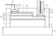
도 1을 참조하면, 기판(21) 상에 제1 도전형 반도체층(25), 활성층(27) 및 제2 도전현 반도체층(29)을 포함하는 반도체 적층 구조체(30)가 위치하고, 상기 제1 도전형 반도체층(25) 및 제2 도전형 반도체층(29)에 각각 제1 전극(41) 및 제2 전극(42)이 접속되어 있다. 상기 제2 도전형 반도체층(29) 상에 투명 도전층(31)이 위치할 수 있으며, 상기 제2 전극(42)은 투명 도전층(31)에 접속될 수 있다.Referring to FIG. 1, a semiconductor stacked
파장 변환층(50)이 반도체 적층 구조체(30)를 덮는다. 파장 변환층(50)은 제1 전극(41) 및 제2 전극(42)을 노출시키는 개구부들(50a, 50b)을 갖는다. 상기 개구부들(50a, 50b)의 내벽(50c, 50d)은 기판(21)의 상면에 대해 수직하다. 즉, 상기 개구부들(50a, 50b)의 바닥부는 입구와 그 폭이 동일하다.The
상기 파장 변환층(50)을 갖는 발광 다이오드 칩은 인쇄회로기판 또는 리드프레임(91) 등에 실장되며, 상기 파장변환층(50)에 노출된 전극들(41, 42)에 와이어(95)가 본딩된다.The LED chip having the
상기 와이어(95)는 캐필러리(60)를 이용하여 본딩되며, 이때, 상기 전극들(41, 42) 상에 와이어 볼(95a)이 먼저 형성되어 전극에 부착되고, 이어서 캐필러리(60)가 이동함에 따라 캐필러리(60)로부터 와이어(95)가 인출된다. 상기 와이어(95)는 리드프레임(91) 등에 마련된 리드 단자에 연결되어 와이어 본딩 공정이 완료된다.The
그런데, 캐필러리(60)는 도 1에 도시한 바와 같이, 상대적으로 넓은 폭(W)을 갖는다. 파장변환층(50)에 캐필러리(60)가 접촉할 경우, 파장변환층(50)이 손상될 수 있으므로, 상기 개구부(50a, 50b)는 캐필러리(60)를 수용할 수 있도록 상대적으로 넓은 폭으로 형성되어야 한다. 이에 따라, 상기 개구부들(50a, 50b)이 제1 및 제2 전극(41, 42)보다 더 큰 폭을 가지며, 따라서 개구부(50a, 50b)의 바닥부가 제1 및 제2 전극(41, 42)의 주위 영역 상에 위치하게 된다. 그 결과, 반도체 적층 구조체(30)에서 생성된 광의 일부는 파장변환층(50)의 개구부들(50a, 50b)을 통해 파장변환없이 외부로 방출된다. 이에 따라, 제1 및 제2 전극(41, 42) 주위에 예컨대 청색 링(blue ring)과 같은 색 편차가 발생된다.By the way, the capillary 60 has a relatively wide width W, as shown in FIG. When the capillary 60 contacts the
상기 청색 링(blue ring) 등의 색 편차를 제거하기 위해 제1 및 제2 전극(41, 42)의 폭을 상대적으로 넓게 형성할 수 있으나, 전극들(41, 42)이 반도체 적층 구조체(30)로부터 방출되는 광을 차단하기 때문에 광 추출 효율이 감소되어 바람직하지 못하다.The widths of the first and
본 발명은 앞서 설명한 문제점 및 기타 다른 문제점들을 해결할 수 있는 기술적 특징을 제공한다. 이하, 본 발명의 실시예들에 대해 상세하게 설명한다.The present invention provides technical features that can solve the above and other problems. Hereinafter, embodiments of the present invention will be described in detail.
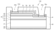
도 2는 본 발명의 일 실시예에 따른 발광 다이오드 칩(100)을 설명하기 위한 단면도이다.2 is a cross-sectional view for describing a light emitting
발광 다이오드 칩(100)은 기판(21), 제1 도전형 반도체층(25), 활성층(27) 및 제2 도전형 반도체층(29)을 포함하는 질화갈륨계 반도체 적층 구조체(30), 제1 전극(41), 제2 전극(42), 및 파장 변환층(50)을 포함한다. 또한, 상기 발광 다이오드 칩(100)은 버퍼층(23), 투명 도전층(31), 절연층(33), 응력 완화층(35) 및 상부 분포 브래그 반사기(37), 하부 분포 브래그 반사기(45) 및 금속층(47)을 포함할 수 있다.The light emitting
기판(21)은 반도체 적층 구조체가 위치하는 상면, 상기 상면에 대향하는 하면, 상면과 하면을 연결하는 측면을 갖는다. 기판(21)은 특별히 한정되지 않으며, 질화물 반도체층을 성장시킬 수 있는 기판, 예컨대 사파이어, 실리콘 탄화물, 스피넬, 또는 실리콘 등일 수 있다. 기판(21)은 반도체 적층 구조체에 비해 상대적으로 두꺼울 수 있으며, 반도체 적층 구조체에서 생성된 광의 일부가 기판(21)의 측면을 통해 방출될 수 있다.The
상기 활성층(27), 상기 제1 및 제2 도전형 반도체층들(25, 29)은 III-N 계열의 화합물 반도체, 예컨대 (Al, Ga, In)N 반도체로 형성될 수 있다. 상기 제1 및 제2 도전형 반도체층들(25, 29)은 각각 단일층 또는 다중층일 수 있다. 예를 들어, 상기 제1 도전형 및/또는 제2 도전형 반도체층(25, 29)은 콘택층과 클래드층을 포함할 수 있으며, 또한 초격자층을 포함할 수 있다. 또한, 상기 활성층(27)은 단일 양자우물 구조 또는 다중 양자우물 구조일 수 있다. 예컨대, 상기 제1 도전형은 n형이고, 상기 제2 도전형은 p형일 수 있으나, 이에 한정되는 것은 아니며, 그 반대일 수 있다. 버퍼층(23)은 기판(21)과 제1 도전형 반도체층(25) 사이에서 격자 부정합을 완화하여 반도체층들(25, 27, 29) 내에 발생되는 결함밀도를 감소시킨다.The
한편, 제1 전극(41)은 제1 도전형 반도체층(25)의 노출된 표면에 접촉하여 제1 도전형 반도체층(27)에 전기적으로 접속할 수 있다. 또한, 제2 전극(42)은 제2 도전형 반도체층(29) 상부에 위치하여 제2 도전형 반도체층(29)에 전기적으로 접속한다. 제1 전극(41) 및 제2 전극(42)은 예컨대, Ti, Cu, Ni, Al, Au 또는 Cr을 포함할 수 있으며 이들 중 2개 이상의 물질로 형성될 수도 있다. 또한, 전류 분산을 위해 Ni/Au, ITO, IZO, ZnO와 같은 투명 도전층(31)이 제2 도전형 반도체층(29) 상에 형성될 수 있으며, 제2 전극(42)은 상기 투명 도전층에 접속할 수 있다. 상기 제1 전극(41) 및 제2 전극(42)의 두께는 특별히 한정되는 것은 아니며, 예컨대 100~200㎛의 두께로 형성될 수 있다.Meanwhile, the
한편, 절연층(33)이 상기 반도체 적층 구조체(30) 및 투명 도전층(31)의 상부를 덮을 수 있다. 절연층(33)은 예컨대, 실리콘 질화물 또는 실리콘 산화물로 형성될 수 있다. 또한, 상기 절연층(33)은 굴절률이 다른 절연층들, 예컨대 SiO2/TiO2 또는 SiO2/Nb2O5를 교대로 적층한 분포 브래그 반사기로 형성될 수 있다. 이 경우, 굴절률이 다른 절연층들의 광학 두께를 조절함으로써, 상기 절연층(33)은 활성층(27)에서 생성된 광을 투과시키고, 외부에서 입사되거나 파장 변환층(50)에서 변환된 광을 반사시킬 수 있다. 이러한 분포 브래그 반사기는 가시광 영역 중 장파장 영역의 광을 반사시키고, 활성층(27)에서 생성된 단파장 가시광 또는 자외선을 투과시키는 반사 대역을 갖는다. 특히, TiO2에 비해 Nb2O5의 광 흡수율이 상대적으로 작기 때문에, SiO2/Nb2O5를 이용하여 분포 브래그 반사기를 형성하는 것이 광 손실을 방지하기 위해 더 바람직하다.The insulating
한편, 응력 완화층(35)이 반도체 적층 구조체(30) 상부, 예컨대 절연층(33) 상에 위치하고, 그 위에 상부 분포 브래그 반사기(37)가 위치할 수 있다.Meanwhile, the
상기 상부 분포 브래그 반사기(37)는 굴절률이 다른 절연층들, 예컨대 SiO2/TiO2 또는 SiO2/Nb2O5를 교대로 적층하여 형성될 수 있다. 이 경우, 굴절률이 다른 절연층들의 광학 두께를 조절함으로써, 상기 상부 분포 브래그 반사기(37)는 활성층(27)에서 생성된 광을 투과시키고, 외부에서 입사되거나 파장 변환층(50)에서 변환된 광을 반사시킬 수 있다. 상기 상부 분포 브래그 반사기(37)는 가시광 영역 중 장파장 영역의 광을 반사시키고, 활성층(27)에서 생성된 단파장 가시광 또는 자외선을 투과시키는 반사 대역을 갖는다. 특히, TiO2에 비해 Nb2O5의 광 흡수율이 상대적으로 작기 때문에, SiO2/Nb2O5를 이용하여 분포 브래그 반사기를 형성하는 것이 광 손실을 방지하기 위해 더 바람직하다.The upper
한편, 응력 완화층(35)은 스핀 온 글래스(SOG) 또는 다공성 실리콘 산화막으로 형성될 수 있다. 상기 응력 완화층(35)은 상기 상부 분포 브래그 반사기(37)의 응력을 완화하여 상부 분포 브래그 반사기(37)의 박리를 방지한다.The
굴절률이 다른 절연층들, 예컨대 SiO2/TiO2 또는 SiO2/Nb2O5를 교대로 적층하여 상부 분포 브래그 반사기(37)를 형성할 경우, 상대적으로 고밀도의 층들이 적층되기 때문에, 분포 브래그 반사기에 생기는 응력이 커진다. 이에 따라 분포 브래그 반사기가 그 아래의 층, 예컨대 절연층(33)으로부터 박리되기 쉽다. 따라서, 응력 완화층(35)을 상부 분포 브래그 반사기(37) 하부에 배치함으로써 상부 분포 브래그 반사기(37)의 박리를 방지할 수 있다.When insulating layers having different refractive indices, such as SiO 2 / TiO 2 or SiO 2 / Nb 2 O 5, are alternately stacked to form the upper
상기 상부 분포 브래그 반사기(37)를 채택하는 경우, 상기 절연층(33)은 단일층, 예컨대 실리콘 질화물 또는 실리콘 산화물로 형성될 수 있으며, 생략될 수도 있다.When the upper
한편, 상기 기판(21)의 하부에 하부 분포 브래그 반사기(45)가 위치한다. 상기 하부 분포 브래그 반사기(45)는 굴절률이 서로 다른 층들을 교대로 적층함으로써 형성되며, 청색 파장 영역의 광, 예컨대 활성층(27)에서 생성된 광뿐만 아니라, 황색 파장 영역의 광 혹은 녹색 및/또는 적색 파장 영역의 광에 대해서도 상대적으로 높은, 바람직하게 90% 이상, 더 바람직하게는 99% 이상의 반사율을 갖는다. 나아가, 상기 하부 분포 브래그 반사기(45)는 예컨대 400~700nm의 파장 범위에 걸쳐 전체적으로 90% 이상, 바람직하게는 99% 이상의 반사율을 가질 수도 있다.The lower
넓은 파장 영역에 걸쳐 상대적으로 높은 반사율을 갖는 하부 분포 브래그 반사기(45)는 반복 적층되는 재료층들의 각 광학 두께를 제어함으로써 형성된다. 상기 하부 분포 브래그 반사기(45)는 예컨대, SiO2의 제1층과 TiO2의 제2층을 교대로 적층하여 형성되거나, SiO2의 제1층과 Nb2O5의 제2층을 교대로 적층하여 형성될 수 있다. TiO2에 비해 Nb2O5의 광 흡수율이 상대적으로 작기 때문에, SiO2의 제1층과 Nb2O5의 제2층을 교대로 적층하는 것이 더 바람직하다. 제1층과 제2층의 적층수가 증가할수록 분포 브래그 반사기(45)의 반사율이 더욱 안정적이며, 예컨대, 분포 브래그 반사기(45)의 적층수는 50층 이상, 즉 25쌍 이상일 수 있다.The lower
교대로 적층되는 제1층들 또는 제2층들이 모두 동일한 두께를 가질 필요는 없으며, 활성층(27)에서 생성된 광의 파장뿐만 아니라 가시영역의 다른 파장에 대해서도 상대적으로 높은 반사율을 갖도록 제1층들 및 제2층들의 두께가 선택된다. 또한, 특정 파장 대역에 대해 반사율이 높은 복수의 분포 브래그 반사기들을 적층하여 상기 하부 분포 브래그 반사기(45)를 형성할 수도 있다.The first or second layers stacked alternately do not have to have the same thickness, and the first layers and the first layers and the first layers and the second layers do not have to have the same thickness, but have relatively high reflectance not only for the wavelength of the light generated in the
상기 하부 분포 브래그 반사기(45)를 채택함으로써, 파장변환층(50)에서 변환된 광이 다시 기판(21)쪽으로 입사될 때, 이 입사된 광을 다시 반사시켜 외부로 방출할 수 있으며, 따라서 광 효율을 개선할 수 있다.By adopting the lower
한편, 상기 분포 브래그 반사기(45)의 첫째층 및 마지막층은 SiO2일 수 있다. SiO2를 분포 브래그 반사기(45)의 첫째층 및 마지막층에 배치함으로써 분포 브래그 반사기(45)를 기판(21)에 안정하게 부착할 수 있고, 또한, 상기 마지막 SiO2층을 이용하여 하부 분포 브래그 반사기(45)를 보호할 수 있다.Meanwhile, the first and last layers of the
금속층(47)은 상기 하부 분포 브래그 반사기(45)의 하부에 위치한다. 상기 금속층(47)은 하부 분포 브래그 반사기(45)를 투과한 광을 반사시키기 위해 알루미늄과 같은 반사 금속으로 형성될 수 있으나, 반사 금속 이외의 금속으로 형성될 수도 있다. 더욱이, 금속층(47)은 적층 구조체(30)에서 생성된 열을 외부로 방출하는 것을 도와, 발광 다이오드 칩(100)의 열 방출 성능을 향상시킨다.The
파장 변환층(50)은 상기 반도체 적층 구조체(30) 상부를 덮는다. 파장 변환층(50)은 에폭시 또는 실리콘에 형광체가 함유되어 형성될 수 있으며, 예컨대, 파장 변환층(50)은 에폭시 또는 실리콘에 형광체를 함유한 후, 이를 스크린 인쇄 등의 방법을 이용하여 도포함으로써 형성될 수 있다. 나아가, 파장 변환층(50)은 예컨대 1.4~2.0 범위 내의 굴절률을 가질 수 있으며, 굴절률을 조절하기 위해 TiO2, SiO2, Y2O3 등의 분말이 파장 변환층(50) 내에 혼입될 수 있다.The
상기 파장 변환층(50)은 제1 전극(41) 및 제2 전극(42)을 각각 노출시키는 개구부들(50a, 50b)을 갖는다. 이들 개구부들(50a, 50b)은 경사진 내벽(50c, 50d)을 갖는다. 또한, 상기 개구부들(50a, 50b)의 바닥부는 각각 제1 전극(41) 및 제2 전극(42)의 전극 영역 상에 한정되어 위치할 수 있다. 상기 바닥부는 대응하는 전극의 전극 영역보다 작은 크기를 가지며, 개구부의 내부에 형성되는 와이어 볼의 폭보다 상대적으로 큰 폭을 가질 수 있다. 한편, 상기 개구부들(50a, 50b)의 입구는 각각 제1 전극(41) 및 제2 전극(42)보다 상대적으로 큰 폭으로 형성될 수 있다. 더욱이, 상기 개구부들(50a, 50b)의 입구는 캐필러리(60)의 폭(W)에 대응하는 크기를 가질 수 있다. 또한, 상기 파장변환층(50) 두께의 1/2 위치에서의 상기 개구부의 폭은 대응하는 전극의 폭, 전극 영역과 대략 동일하거나 그보다 작을 수 있다.The
상기 파장 변환층(50)은 반도체 적층 구조체(30)의 상부를 덮으며, 나아가, 기판(21)의 측면 및 반도체 적층 구조체(30)의 측면을 덮을 수 있다. 따라서, 반도체 적층 구조체(30)의 상면을 통해 방출되는 광뿐만 아니라, 기판(21)의 측면을 통해 방출되는 광에 대해서도 파장 변환을 수행할 수 있는 발광 다이오드 칩(100)이 제공된다. 또한, 파장 변환층(50)의 상면은 평평할 수 있으며, 반도체 적층 구조체(30) 상부의 파장 변화층(50)의 두께와 상기 기판(21) 측면의 파장변환층(50)의 두께는 실질적으로 동일할 수 있다.The
본 실시예에 있어서, 기판(21) 상에 단일의 반도체 적층 구조체(30)가 위치하는 것으로 도시 및 설명하였으나, 기판(21) 상에 복수의 반도체 적층 구조체들이 서로 전기적으로 이격되어 위치할 수 있으며, 상기 파장 변환층(50)이 이들 반도체 적층 구조체들을 덮을 수 있다. 또한, 상기 복수의 반도체 적층 구조체들과 상기 파장 변환층 사이에 도 2의 분포 브래그 반사기(37)와 같은 분포 브래그 반사기가 위치할 수 있으며, 상기 분포 브래그 반사기와 반도체 적층 구조체 사이에 응력 완화층이 개재될 수 있다.In the present exemplary embodiment, a single semiconductor stacked
도 3은 본 발명의 일 실시예에 따른 발광 다이오드 칩(100)을 탑재한 발광 다이오드 패키지를 설명하기 위한 단면도이다.3 is a cross-sectional view illustrating a light emitting diode package equipped with a light emitting
도 3을 참조하면, 발광 다이오드 패키지는, 발광 다이오드 칩(100) 및 발광 다이오드 칩(100)을 탑재하기 위한 마운트(91)를 포함한다. 또한, 상기 발광 다이오드 패키지는 본딩 와이어(95) 및 렌즈(97)를 포함할 수 있다. Referring to FIG. 3, the LED package includes a light emitting
상기 마운트(91)는 예컨대 인쇄회로 기판, 리드 프레임, 세라믹 기판 등일 수 있으며, 리드 단자들(93a, 93b)을 포함한다. 발광 다이오드 칩(100)의 제1 전극(도 2의 41) 및 제2 전극(도 2의 42)이 각각 본딩 와이어(95)를 통해 리드 단자들(93a, 93b)에 전기적으로 연결된다. 이때, 상기 본딩 와이어(95)의 와이어 볼(95a)은 파장 변환층(50)의 개구부들(50a, 50b) 내부에 위치한다. 즉, 와이어 볼(95a)은 파장변환층(50) 개구부(50a, 50b)의 입구 아래에 위치한다.The
한편, 렌즈(97)가 발광 다이오드 칩(100)을 덮는다. 렌즈(97)는 발광 다이오드 칩(100)에서 방출된 광의 지향각을 조절하여 원하는 방향으로 광이 방출되도록 한다. 발광 다이오드 칩(100)에 파장 변환층(50)이 형성되어 있으므로, 상기 렌즈(97)는 형광체를 함유할 필요가 없다.On the other hand, the
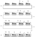
이하, 본 발명의 일 실시예에 따른 발광 다이오드 칩(100) 제조 방법에 대해 도 4를 참조하여 구체적으로 설명한다. Hereinafter, a method of manufacturing a light emitting
도 4(a)를 참조하면, 지지 기판(101) 상에 배어 칩들(150)이 배열된다. 배어 칩들(150)은 등간격으로 지지 기판(101) 상에 배열될 수 있다. 배어 칩들(150)은, 도 2에 도시된 바와 같이, 기판(21), 제1 도전형 반도체층(25), 활성층(27) 및 제2 도전형 반도체층(29)을 포함하는 질화갈륨계 반도체 적층 구조체(30), 제1 전극(41), 제2 전극(42)을 포함한다. 또한, 제1 도전형 반도체층(25)과 기판(21) 사이에 버퍼층(23)이 개재될 수 있다. 나아가, 상기 배어 칩들(150)은 투명 도전층(31) 및 절연층(33)을 포함할 수 있으며, 응력완화층(35) 및 상부 분포 브래그 반사기(37), 하부 분포 브래그 반사기(45) 및 금속층(47)을 포함할 수 있다. 즉, 상기 배어 칩(150)은 도 2의 발광 다이오드 칩(100)에서 파장 변환층(50)을 제외한 부분에 해당하며, 중복을 피하기 위해 배어칩(150)의 각 구성 요소에 대한 상세한 설명은 생략한다.Referring to FIG. 4A,
지지 기판(101)은 배어 칩들(150)이 등간격을 유지하도록 지지한다. 지지기판(101)은 예컨대, 글래스, 세라믹, 사파이어, GaN, Si 등의 기판일 수 있다.The
도 4(b)를 참조하면, 상기 지지 기판(101) 상에서 상기 배어 칩들(150), 제1 및 제2 전극들(41, 42)을 덮는 파장 변환층(50)이 형성된다. 파장 변환층(50)은 형광체를 함유할 수 있으며, 또한 굴절률을 제어하기 위해 TiO2, SiO2, Y2O3 등의 분말을 함유할 수 있다. 상기 파장 변환층(50)은 제1 및 제2 전극들(41, 42)을 덮도록 충분히 두껍게 형성되며 그 상면은 평평한 형상을 갖는다. 상기 파장변환층(50)은 또한, 배어칩들(150) 사이의 영역을 채워 각 배어칩들(150)의 기판(21) 측면을 덮는다. 파장 변환층(50)은 인젝션 몰딩, 트랜스퍼 몰딩, 컴프레션 몰딩, 프린팅 등 다양한 도포 방법에 의해 형성될 수 있다.Referring to FIG. 4B, a
도 4(c)를 참조하면, 파장 변환층(50)이 형성된 후, 상기 각 배어칩들의 제1 및 제2 전극들(41, 42)을 노출시키는 개구부들(50a, 50b)이 형성된다. 상기 개구부들(50a, 50b)은 도 2를 참조하여 설명한 바와 같이 경사진 내벽을 갖도록 형성된다. 상기 개구부들(50a, 50b)은 레이저 빔, 예를 들어 CO2 레이저를 이용한 레이저 빔을 사용하여 형성될 수 있다. CO2 레이저는 약 10㎛ 파장의 레이저 빔을 방출하며, 이 레이저 빔을 이용함으로써 전극들(41, 42)을 손상시키지 않고 개구부들(50a, 50b)을 형성할 수 있다. 개구부들(50a, 50b)을 형성한 후, 전극들(41, 42) 상에 잔류하는 형광체 또는 수지는 습식 또는 건식 세정에 의해 제거될 수 있다.Referring to FIG. 4C, after the
도 4(d)를 참조하면, 상기 개구부가 형성된 후, 지지기판(101)이 제거된다. 지지기판(101)을 쉽게 제거하기 위해, 지지기판(101) 상에 박리 필름(도시하지 않음)이 형성될 수도 있다. 이러한 박리 필름은 예컨대 열 또는 자외선 등의 광에 의해 박리되는 필름일 수 있다. 따라서, 이러한 박리 필름에 열을 가하거나 자외선 등의 광을 조사함으로써 지지기판(101)이 용이하게 제거될 수 있다.Referring to Figure 4 (d), after the opening is formed, the
그 후, 상기 배어칩들(150)을 덮는 파장 변환층(50)을 분할하여 파장변환층(50)을 갖는 개별 발광 다이오드 칩들(100)을 완성한다. 상기 지지기판(101)을 제거하기 전에 파장변환층(50)을 먼저 분할하고, 그 후 지지기판(101)을 제거할 수도 있다. 상기 파장변환층(50)은 블레이드를 이용하거나 또는 레이저를 이용하여 분할될 수 있다. Thereafter, the
한편, 본 실시예에 있어서, 기판(21) 상에 단일의 반도체 적층 구조체를 포함하는 것으로 설명하였으나, 배어 칩(150)은 복수의 반도체 적층 구조체(30)를 포함할 수 있으며, 또한 상기 반도체 적층 구조체들(30)을 전기적으로 연결하는 배선들을 포함할 수 있다.On the other hand, in the present embodiment, it has been described as including a single semiconductor stack structure on the
도 5는 본 발명의 또 다른 실시예에 따른 발광 다이오드 칩(200)을 설명하기 위한 개략적인 단면도이다.5 is a schematic cross-sectional view for describing a light emitting
도 5를 참조하면, 본 실시예에 따른 발광 다이오드 칩(200)은 도 2를 참조하여 설명한 발광 다이오드 칩(100)과 대체로 유사하나, 파장변환층(50)이 기판(21) 상부에 위치하는 것에 차이가 있다. 즉, 파장변환층(50)은 기판(21)의 측면을 덮지 않는다. 이러한 발광 다이오드 칩(200)은 기판(21)을 분할하기 전에 파장변환층(50)을 기판(21) 상에서 즉, 웨이퍼 레벨에서 형성함으로써 제조된다. 상기 파장 변환층(50)은 기판(21)의 상면에 접할 수도 있으나, 이에 한정되는 것은 아니며, 제1 도전형 반도체층(25) 상부에 위치할 수도 있다.Referring to FIG. 5, the light emitting
한편, 개구부들(50a, 50b)은 기판(21)을 분할하기 전에 형성될 수도 있으나, 이에 한정되는 것은 아니며, 기판(21)을 분할한 후에 형성될 수도 있다.The
도 6은 본 발명의 또 다른 실시예에 따른 발광 다이오드 칩(300)을 설명하기 위한 개략적인 단면도이다.6 is a schematic cross-sectional view for describing a light emitting
도 6을 참조하면, 앞서 설명한 발광 다이오드 칩들(100, 200)은 수평형 구조를 갖지만, 본 실시예에 따른 발광 다이오드 칩(300)은 수직형 구조를 갖는 것에 차이가 있다.Referring to FIG. 6, the
상기 발광 다이오드 칩(300)은 기판(51), 제1 도전형 반도체층(25), 활성층(27) 및 제2 도전형 반도체층(29)을 포함하는 반도체 적층 구조체(30), 상부 전극(41) 및 파장 변환층(60)을 포함한다. 상기 발광 다이오드 칩(300)은 또한, 도 2를 참조하여 설명한 바와 같이, 절연층(33), 응력 완화층(35) 및 상부 분포 브래그 반사기(37)를 포함할 수 있다. 나아가, 상기 발광 다이오드 칩(104)은 반사 금속층(55), 장벽 금속층(57) 및 본딩 금속(53)을 포함할 수 있다.The light emitting
기판(51)은 반도체층들(25, 27, 29)을 성장시키기 위한 성장기판과 구분되며, 이미 성장된 화합물 반도체층들(25, 27, 29)에 부착된 2차 기판이다. 상기 기판(51)은 도전성 기판, 예컨대 금속 기판 또는 반도체 기판일 수 있으나, 이에 한정되는 것은 아니며, 사파이어와 같은 절연 기판일 수도 있다.The
반도체 적층 구조체(30)는 기판(51) 상에 위치하며, 제1 도전형 반도체층(25), 활성층(27) 및 제2 도전형 반도체층(29)을 포함한다. 여기서, 상기 반도체 적층 구조체(30)는 일반적인 수직형 발광 다이오드와 같이 p형 화합물 반도체층(29)이 n형 화합물 반도체층(25)에 비해 기판(51) 측에 가깝게 위치한다. 상기 반도체 적층 구조체(30)는 기판(51)의 일부 영역 상에 위치할 수 있다. 즉, 기판(51)이 반도체 적층 구조체(30)에 비해 상대적으로 넓은 면적을 가지며, 반도체 적층 구조체(30)는 상기 기판(51)의 가장자리로 둘러싸인 영역 내에 위치할 수 있다.The semiconductor stacked
상기 제1 도전형 반도체층(25), 활성층(27) 및 제2 도전형 반도체층(29)은 도 1을 참조하여 설명한 반도체층들과 유사하므로 상세한 설명은 생략한다. 한편, 저항이 상대적으로 작은 n형 화합물 반도체층(25)을 기판(51)의 반대쪽에 위치하도록 함으로써 n형 화합물 반도체층(25)의 상부면에 거칠어진 표면이 형성될 수 있다. 한편, 상부 전극(41)이 반도체 적층 구조체(30), 예컨대 제1 도전형 반도체층(25) 상에 위치하여 제1 도전형 반도체층(25)에 전기적으로 접속된다.Since the first
상기 기판(51)과 반도체 적층 구조체(30) 사이에 반사 금속층(55)이 개재될 수 있으며, 장벽 금속층(57)이 기판(51)과 반사 금속층(55) 사이에 개재되어 반사 금속층(55)을 둘러쌀 수 있다. 나아가, 상기 기판(51)은 본딩 금속(53)을 통해 반도체 적층 구조체(30)에 본딩될 수 있다. 상기 반사 금속층(55) 및 상기 장벽 금속층(57)이 상기 제2 도전형 반도체층(29)에 전기적으로 접속된 하부 전극으로 기능할 수 있다.A
절연층(33)이 반도체 적층 구조체(30)의 상부면을 덮고, 그 위에 차례로 응력 완화층(35) 및 상부 분포 브래그 반사기(37)가 위치할 수 있다. 상기 절연층(33), 응력 완화층(35) 및 상부 분포 브래그 반사기(37)는 도 2를 참조하여 설명한 것과 동일한 재질로 형성될 수 있으므로 중복을 피하기 위해 상세한 설명은 생략한다. 또한, 상기 절연층(33)은 생략될 수도 있다. 또한, 상기 절연층(33)은 도 2의 실시예에서 설명한 바와 같이 분포 브래그 반사기일 수 있으며, 이 경우, 응력 완화층(35) 및 상부 분포 브래그 반사기(37)는 생략될 수 있다.An insulating
한편, 상기 반도체 적층 구조체(30) 상부에 파장변환층(60)이 위치한다. 상기 절연층(33), 응력 완화층(35) 및 분포 브래그 반사기(37)는 상기 파장변환층(60)과 반도체 적층 구조체(30) 사이에 위치한다. 상기 파장변환층(60)은 상기 반도체 적층 구조체(30) 상부에 한정되어 위치할 수 있으나, 이에 한정되는 것은 아니며, 상기 반도체 적층 구조체(30)의 측면, 나아가 상기 기판(51)의 측면을 덮을 수도 있다. 상기 파장변환층(60)은 상기 상부 전극(41)을 노출시키는 개구부(60a)를 가지며, 상기 개구부(60a)의 내벽(60c)은 도 2를 참조하여 설명한 바와 같이, 상기 기판(51)의 상면에 대해 경사져 있다. 상기 개구부(60a)는 앞서 도 2를 참조하여 설명한 개구부(50a, 50b)와 동일하므로 상세한 설명은 생략한다.Meanwhile, the
본 실시예에 있어서, 상기 파장변환층(60)은 기판(51)을 개별 칩 단위로 분할하기 전에 형성될 수 있으나, 이에 한정되는 것은 아니며 배어 칩으로 분할한 후에 형성될 수도 있다. In the present exemplary embodiment, the
Claims (18)
상기 기판의 상면에 위치하는 질화갈륨계 화합물 반도체 적층 구조체로서, 제1 도전형 반도체층, 활성층 및 제2 도전형 반도체층을 포함하는 반도체 적층 구조체;
상기 반도체 적층 구조체에 전기적으로 접속된 전극; 및
상기 반도체 적층 구조체의 상부를 덮되, 상기 전극을 노출시키는 개구부를 갖는 파장변환층을 포함하고,
상기 개구부는 상기 기판의 상면에 대해 경사진 내벽을 갖는 발광 다이오드 칩.A substrate having a top surface, a bottom surface, and side surfaces connecting the top surface and the bottom surface;
A gallium nitride compound semiconductor stacked structure disposed on an upper surface of the substrate, comprising: a semiconductor stacked structure including a first conductive semiconductor layer, an active layer, and a second conductive semiconductor layer;
An electrode electrically connected to the semiconductor laminate structure; And
A wavelength conversion layer covering an upper portion of the semiconductor laminate structure and having an opening exposing the electrode;
The opening has a light emitting diode chip having an inner wall inclined with respect to the upper surface of the substrate.
상기 파장변환층의 표면에 위치하는 상기 개구부의 입구는 상기 개구부의 바닥부에 비해 상대적으로 넓은 폭을 갖고, 상기 개구부의 바닥부는 상기 전극 영역 상에 한정되어 위치하는 발광 다이오드 칩.The method according to claim 1,
The inlet of the opening located on the surface of the wavelength conversion layer has a relatively wider width than the bottom of the opening, the bottom portion of the opening LED chip is located on the electrode area limited.
상기 개구부의 입구는 상기 전극 영역에 비해 상대적으로 넓은 폭을 갖는 발광 다이오드 칩.The method according to claim 2,
The opening of the opening is a light emitting diode chip having a relatively wider width than the electrode area.
상기 파장변환층 두께의 1/2 위치에서 상기 개구부의 폭은 상기 전극 영역에 비해 상대적으로 좁은 발광 다이오드 칩.The method according to claim 3,
The width of the opening at a position 1/2 of the thickness of the wavelength conversion layer is relatively narrow compared to the electrode area.
상기 파장변환층은 상기 반도체 적층 구조체의 측면 및 상기 기판의 측면을 덮는 발광 다이오드 칩.The method according to claim 1,
The wavelength conversion layer is a light emitting diode chip covering the side of the semiconductor laminated structure and the side of the substrate.
상기 파장변환층과 상기 반도체 적층 구조체 사이에 개재된 분포 브래그 반사기를 더 포함하는 발광 다이오드 칩.The method according to claim 1,
And a distributed Bragg reflector interposed between the wavelength conversion layer and the semiconductor stacked structure.
상기 분포 브래그 반사기와 상기 반도체 적층 구조체 사이에 개재된 응력 완화층을 더 포함하는 발광 다이오드 칩.The method of claim 7,
And a stress relaxation layer interposed between the distributed Bragg reflector and the semiconductor laminate.
상기 응력 완화층은 SOG 또는 다공성 실리콘 산화막으로 형성된 발광 다이오드 칩.The method according to claim 8,
The stress relief layer is a light emitting diode chip formed of SOG or porous silicon oxide film.
청구항 1 내지 9의 어느 한 항에 기재된 발광 다이오드 칩; 및
상기 발광 다이오드 칩의 전극과 상기 리드 단자를 연결하는 본딩와이어를 포함하는 발광 다이오드 패키지.Lead terminals;
The light emitting diode chip according to any one of claims 1 to 9; And
And a bonding wire connecting the electrode of the light emitting diode chip to the lead terminal.
상기 본딩와이어의 와이어 볼은 상기 파장 변환층의 개구부 내에 위치하는 발광 다이오드 패키지.The method according to claim 10,
The wire ball of the bonding wire is located in the opening of the wavelength conversion layer.
상기 지지 기판 상에서 상기 복수개의 배어 칩들을 덮는 파장변환층을 형성하고,
상기 파장변환층을 패터닝하여 상기 전극들을 노출시키는 개구부들을 형성하는 것을 포함하되,
상기 개구부는 상기 기판의 상면에 대해 경사진 내벽을 갖는 발광 다이오드 칩 제조 방법.A plurality of bare chips are arranged on a supporting substrate, wherein each bare chip comprises a substrate having a top surface, a bottom surface, and side surfaces connecting the top surface and the bottom surface, and a gallium nitride compound semiconductor stacked structure positioned on the top surface of the substrate. A semiconductor laminated structure comprising a first conductive semiconductor layer, an active layer and a second conductive semiconductor layer, and an electrode electrically connected to the semiconductor laminated structure,
Forming a wavelength conversion layer covering the plurality of bare chips on the support substrate;
Patterning the wavelength conversion layer to form openings exposing the electrodes,
The opening has a light emitting diode chip manufacturing method having an inner wall inclined with respect to the upper surface of the substrate.
상기 파장변환층의 표면에 위치하는 상기 개구부의 입구는 상기 개구부의 바닥부에 비해 상대적으로 넓은 폭을 갖고, 상기 개구부의 바닥부는 상기 전극 영역 상에 한정되어 위치하는 발광 다이오드 칩 제조 방법.The method of claim 12,
The inlet of the opening located on the surface of the wavelength conversion layer has a relatively wider width than the bottom of the opening, the bottom portion of the opening is a LED chip manufacturing method is limited to the electrode area.
상기 개구부들은 레이저 빔을 조사하여 형성되는 발광 다이오드 칩 제조 방법.The method of claim 12,
The openings are formed by irradiating a laser beam.
상기 레이저 빔은 CO2 레이저에 의해 형성되는 발광 다이오드 칩 제조 방법.The method according to claim 14,
The laser beam is a light emitting diode chip manufacturing method of the CO 2 laser.
상기 배어 칩은
상기 반도체 적층 구조체 상부에 위치하는 분포 브래그 반사기; 및
상기 분포 브래그 반사기와 상기 반도체 적층 구조체 사이에 개재된 응력 완화층을 더 포함하는 발광 다이오드 칩 제조 방법.The method of claim 12,
The bare chip
A distributed Bragg reflector positioned above the semiconductor laminate structure; And
And a stress relaxation layer interposed between the distributed Bragg reflector and the semiconductor laminate.
상기 개구부가 형성된 후, 상기 파장 변환층을 분할하여 개별 발광 다이오드 칩들로 분할하고,
상기 지지 기판을 제거하는 것을 더 포함하는 발광 다이오드 칩 제조 방법.The method of claim 12,
After the opening is formed, the wavelength conversion layer is divided into individual light emitting diode chips,
And removing the support substrate.
상기 파장 변환층을 분할하는 것은 상기 지지 기판을 제거한 후에 수행되는 발광 다이오드 칩 제조 방법.18. The method of claim 17,
The dividing of the wavelength conversion layer is performed after removing the support substrate.
Priority Applications (1)
| Application Number | Priority Date | Filing Date | Title |
|---|---|---|---|
| KR1020100115082A KR101752425B1 (en) | 2010-11-18 | 2010-11-18 | Light emitting diode chip having wavelength converting layer, method of fabricating the same and package having the same |
Applications Claiming Priority (1)
| Application Number | Priority Date | Filing Date | Title |
|---|---|---|---|
| KR1020100115082A KR101752425B1 (en) | 2010-11-18 | 2010-11-18 | Light emitting diode chip having wavelength converting layer, method of fabricating the same and package having the same |
Publications (2)
| Publication Number | Publication Date |
|---|---|
| KR20120053784A true KR20120053784A (en) | 2012-05-29 |
| KR101752425B1 KR101752425B1 (en) | 2017-07-11 |
Family
ID=46269864
Family Applications (1)
| Application Number | Title | Priority Date | Filing Date |
|---|---|---|---|
| KR1020100115082A KR101752425B1 (en) | 2010-11-18 | 2010-11-18 | Light emitting diode chip having wavelength converting layer, method of fabricating the same and package having the same |
Country Status (1)
| Country | Link |
|---|---|
| KR (1) | KR101752425B1 (en) |
Cited By (7)
| Publication number | Priority date | Publication date | Assignee | Title |
|---|---|---|---|---|
| WO2014014300A3 (en) * | 2012-07-18 | 2014-03-13 | 주식회사 세미콘라이트 | Semiconductor light-emitting element |
| KR101419867B1 (en) * | 2012-09-05 | 2014-07-16 | 주식회사 세미콘라이트 | Semiconductor light emimitting device |
| KR101427316B1 (en) * | 2012-09-05 | 2014-08-06 | 주식회사 세미콘라이트 | Semiconductor light emimitting device |
| US9236524B2 (en) | 2012-07-18 | 2016-01-12 | Semicon Light Co., Ltd. | Method of manufacturing semiconductor light emitting device |
| US9466768B2 (en) | 2012-01-13 | 2016-10-11 | Semicon Light Co., Ltd. | Semiconductor light emitting device with a light-reflecting face |
| KR20180095426A (en) * | 2017-02-17 | 2018-08-27 | 서울바이오시스 주식회사 | Light emitting diode having side reflection layer |
| US10535798B2 (en) | 2012-07-18 | 2020-01-14 | Semicon Light Co., Ltd. | Semiconductor light emitting device comprising finger electrodes |
Families Citing this family (1)
| Publication number | Priority date | Publication date | Assignee | Title |
|---|---|---|---|---|
| KR102607596B1 (en) | 2018-05-11 | 2023-11-29 | 삼성전자주식회사 | Semiconductor light emitting device and semiconductor light emitting device package using the same |
Family Cites Families (1)
| Publication number | Priority date | Publication date | Assignee | Title |
|---|---|---|---|---|
| US20100105156A1 (en) * | 2008-10-27 | 2010-04-29 | Po-Shen Chen | Method of manufacturing light-emitting diode package |
-
2010
- 2010-11-18 KR KR1020100115082A patent/KR101752425B1/en active IP Right Grant
Cited By (11)
| Publication number | Priority date | Publication date | Assignee | Title |
|---|---|---|---|---|
| US9466768B2 (en) | 2012-01-13 | 2016-10-11 | Semicon Light Co., Ltd. | Semiconductor light emitting device with a light-reflecting face |
| WO2014014300A3 (en) * | 2012-07-18 | 2014-03-13 | 주식회사 세미콘라이트 | Semiconductor light-emitting element |
| CN103988322A (en) * | 2012-07-18 | 2014-08-13 | 世迈克琉明有限公司 | Semiconductor light-emitting element |
| US9236524B2 (en) | 2012-07-18 | 2016-01-12 | Semicon Light Co., Ltd. | Method of manufacturing semiconductor light emitting device |
| CN103988322B (en) * | 2012-07-18 | 2016-10-12 | 世迈克琉明有限公司 | Light emitting semiconductor device |
| US9530941B2 (en) | 2012-07-18 | 2016-12-27 | Semicon Light Co., Ltd. | Semiconductor light emitting device |
| US10535798B2 (en) | 2012-07-18 | 2020-01-14 | Semicon Light Co., Ltd. | Semiconductor light emitting device comprising finger electrodes |
| EP2782148B1 (en) * | 2012-07-18 | 2020-05-06 | Semicon Light Co. Ltd. | Semiconductor light-emitting device |
| KR101419867B1 (en) * | 2012-09-05 | 2014-07-16 | 주식회사 세미콘라이트 | Semiconductor light emimitting device |
| KR101427316B1 (en) * | 2012-09-05 | 2014-08-06 | 주식회사 세미콘라이트 | Semiconductor light emimitting device |
| KR20180095426A (en) * | 2017-02-17 | 2018-08-27 | 서울바이오시스 주식회사 | Light emitting diode having side reflection layer |
Also Published As
| Publication number | Publication date |
|---|---|
| KR101752425B1 (en) | 2017-07-11 |
Similar Documents
| Publication | Publication Date | Title |
|---|---|---|
| US10043955B2 (en) | Light emitting diode chip having wavelength converting layer and method of fabricating the same, and package having the light emitting diode chip and method of fabricating the same | |
| EP3364469B1 (en) | Light emitting diode having side reflection layer | |
| US10580929B2 (en) | UV light emitting diode package and light emitting diode module having the same | |
| KR102641239B1 (en) | Light emitting diode, method of fabricating the same, and light emitting device module having the same | |
| KR101142965B1 (en) | Wafer-level light emitting diode package and method of fabricating the same | |
| US8026527B2 (en) | LED structure | |
| US10340425B2 (en) | Light emitting diode having light blocking layer | |
| US9773950B2 (en) | Semiconductor device structure | |
| US11935990B2 (en) | Light emitting diode having side reflection layer | |
| KR20120092000A (en) | Light emitting device having wavelength converting layer | |
| JP2011243977A (en) | Light emitting diode chip having wavelength converting layer and method of fabricating the same, and package having the light emitting diode chip and method of fabricating the same | |
| KR101752425B1 (en) | Light emitting diode chip having wavelength converting layer, method of fabricating the same and package having the same | |
| JP2012124443A (en) | Semiconductor light emitting device and manufacturing method of the same | |
| KR20160046538A (en) | Light emitting device and method of fabricating the same | |
| KR101230619B1 (en) | Light emitting diode chip having wavelength converting layer, method of fabricating the same and package having the same | |
| WO2016038757A1 (en) | Semiconductor light emitting device | |
| KR20160149827A (en) | Light emitting device including multiple wavelength conversion units and method of making the same | |
| US11749792B2 (en) | Light emitting diode, light emitting diode module, and display device including the same | |
| KR20120031473A (en) | Wafer-level light emitting diode package having plurality of light emitting cells and method of fabricating the same | |
| KR20220004002A (en) | Light emitting device | |
| KR102464320B1 (en) | Light emitting device package | |
| KR20130110131A (en) | Light emitting diode chip having wavelength converting layer, method of fabricating the same and package having the same | |
| KR20120031472A (en) | Wafer-level light emitting diode package and method of fabricating the same | |
| KR20180097979A (en) | Light emitting diode having light blocking layer | |
| KR20150069228A (en) | Light emitting diode with wavelength conversion layer and method of fabricating the same |
Legal Events
| Date | Code | Title | Description |
|---|---|---|---|
| E902 | Notification of reason for refusal | ||
| E701 | Decision to grant or registration of patent right | ||
| GRNT | Written decision to grant |