KR20120005291A - 임피던스 캘리브레이션 회로 및 그 동작 방법 - Google Patents
임피던스 캘리브레이션 회로 및 그 동작 방법 Download PDFInfo
- Publication number
- KR20120005291A KR20120005291A KR1020100065961A KR20100065961A KR20120005291A KR 20120005291 A KR20120005291 A KR 20120005291A KR 1020100065961 A KR1020100065961 A KR 1020100065961A KR 20100065961 A KR20100065961 A KR 20100065961A KR 20120005291 A KR20120005291 A KR 20120005291A
- Authority
- KR
- South Korea
- Prior art keywords
- signal
- calibration
- mode
- generator
- input
- Prior art date
- Legal status (The legal status is an assumption and is not a legal conclusion. Google has not performed a legal analysis and makes no representation as to the accuracy of the status listed.)
- Granted
Links
Images


Classifications
-
- H—ELECTRICITY
- H03—ELECTRONIC CIRCUITRY
- H03K—PULSE TECHNIQUE
- H03K19/00—Logic circuits, i.e. having at least two inputs acting on one output; Inverting circuits
- H03K19/0005—Modifications of input or output impedance
Landscapes
- Physics & Mathematics (AREA)
- Engineering & Computer Science (AREA)
- Computer Hardware Design (AREA)
- Computing Systems (AREA)
- General Engineering & Computer Science (AREA)
- Mathematical Physics (AREA)
- Dram (AREA)
Abstract
Description
도 2는 일반적인 풀 업 캘리브레이션 제어 과정도이다.
도 3은 일반적인 풀 다운 캘리브레이션 제어 과정도이다.
도 4는 ZQ 캘리브레이션 제어 과정에 따른 목표 전위 추적 과정도이다.
도 5는 ZQ 캘리브레이션 커맨드 진리표 이다.
도 6은 ZQ 캘리브레이션 타이밍 파라미터 이다.
도 7은 종래 ZQCL 동작 모드, ZQCS 동작 모드 타이밍도 이다.
도 8은 종래 ZQCL 동작 모드 타이밍도이다.
도 9는 본 발명의 실시예에 따른 자동 ZQ 캘리브레이션 모드제어회로도이다.
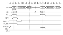
도 10은 본 발명에 따른 ZQCL 동작 모드 타이밍도이다.
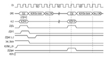
도 11은 본 발명에 따른 ZQCS 동작 모드 타이밍도이다.
6,7 : OP 앰프 8 : 외부저항
30 : 타이밍 튜닝부 31~36 : 낸드게이트
37~41 : 인버터 50 : 지연부
Claims (18)
- 파워 업 후, ZQ 캘리브레이션 커맨드가 입력되면, 제 1 캘리브레이션 제어신호를 발생하는 제 1 신호발생부; 및
리프레쉬 동작 중에 제 2 캘리브레이션 제어신호를 발생하는 제 2 신호발생부
를 포함하는 자동 ZQ 캘리브레이션 모드제어회로.
- 제 1 항에 있어서,
상기 제 2 신호발생부는, 특정 어드레스 신호가 입력되었을 때, 제 2 캘리브레이션 제어신호를 발생하는 자동 ZQ 캘리브레이션 모드제어회로.
- 제 2 항에 있어서,
상기 제 2 신호발생부는,
리프레쉬 커맨드와 특정 어드레스 신호를 연산하여 제 2 캘리브레이션 제어를 위한 펄스신호를 발생하는 연산부를 포함하는 자동 ZQ 캘리브레이션 모드제어회로.
- 제 3 항에 있어서,
상기 특정 어드레스 신호는, 어드레스 <10> 신호인 자동 ZQ 캘리브레이션 모드제어회로.
- 제 4 항에 있어서,
상기 제 2 신호발생부는, 상기 어드레스 <10> 신호를 일정시간 동안 튜닝하는 타이밍 튜닝부를 포함하는 자동 ZQ 캘리브레이션 모드제어회로.
- 제 1 항에 있어서,
상기 제 1 신호발생부는, 캘리브레이션 커맨드신호와, 특정 어드레스신호를 입력하여, 제 1 캘리브레이션 모드신호를 발생하는 연산부를 포함하는 자동 ZQ 캘리브레이션 모드제어회로.
- 제 6 항에 있어서,
상기 제 1 신호발생부는, 특정 어드레스신호를 일정시간 동안 튜닝하는 타이밍 튜닝부를 포함하는 자동 ZQ 캘리브레이션 모드제어회로. - 제 7 항에 있어서,
상기 제 1 신호발생부는, 상기 타이밍 튜닝부의 출력신호를 반전시키는 인버터를 더 포함하는 자동 ZQ 캘리브레이션 모드제어회로.
- 제 6 항에 있어서,
상기 제 1 신호발생부는, 파워 업 후 발생한 상태신호와, 상기 연산부의 출력신호를 입력하여 제 3 캘리브레이션 모드신호에 따른 펄스신호를 발생하는 제 1 펄스발생부를 포함하는 자동 ZQ 캘리브레이션 모드제어회로.
- 제 9 항에 있어서,
상기 제 1 펄스발생부는,
상기 상태신호와 제 1 캘리브레이션 모드신호를 입력하는 낸드게이트; 및
상기 낸드게이트의 출력을 반전하는 인버터를 포함하는 자동 ZQ 캘리브레이션 모드제어회로.
- 제 9 항에 있어서,
상기 제 1 신호발생부는,
상기 제 3 캘리브레이션 모드신호를 지연시키는 지연부; 및
상기 지연부의 지연신호와, 상기 상태신호 그리고 제 1 캘리브레이션 모드신호를 입력하여 제 4 캘리브레이션 모드신호에 따른 펄스신호를 발생하는 제 2 펄스발생부를 포함하는 자동 ZQ 캘리브레이션 모드제어회로.
- 제 11 항에 있어서,
상기 제 2 펄스발생부는,
상기 지연신호와 상태신호 그리고 제 1 캘리브레이션 모드신호를 입력하는 낸드게이트; 및
상기 낸드게이트의 출력을 반전하는 인버터를 포함하는 자동 ZQ 캘리브레이션 모드제어회로.
- 제 9 항에 있어서,
상기 상태신호는, 파워 업 후 발생한 리셋신호를 래치시키는 래치부의 출력신호인 자동 ZQ 캘리브레이션 모드제어회로.
- 제 12 항에 있어서,
상기 제 2 펄스발생부에 입력되는 상태신호는, 제 1 펄스발생부에 입력되는 상태신호를 반전시킨 신호인 자동 ZQ 캘리브레이션 모드제어회로.
- 제 1 항에 있어서,
상기 제 2 캘리브레이션 모드신호가 동작되는 구간에서 리프레쉬 동작 외 다른 동작은 수행되지 않는 자동 ZQ 캘리브레이션 모드제어회로.
- 파워 업 후, 처음의 ZQ 캘리브레이션 커맨드 입력시, 제 1 캘리브레이션 제어신호를 발생하는 제 1 신호발생부;
리프레쉬 동작 중에 제 2 캘리브레이션 제어신호를 발생하는 제 2 신호발생부; 및
캘리브레이션 커맨드와, 일정시간 지연된 제 1 캘리브레이션 제어신호를 입력받아서 제 3 캘리브레이션 제어신호를 발생하는 제 3 신호발생부
를 포함하는 자동 ZQ 캘리브레이션 모드제어회로.
- ZQ 캘리브레이션 커맨드가 입력되면, 제 1 캘리브레이션 제어신호를 발생하는 제 1 신호발생부;
리프레쉬 동작 중에 제 2 캘리브레이션 제어신호를 발생하는 제 2 신호발생부;
파워 업 후, 처음의 ZQ 캘리브레이션 커맨드 입력시, 상기 제 1 캘리브레이션 제어신호를 입력받아서 제 3 캘리브레이션 제어신호를 발생하는 제 3 신호발생부; 및
상기 제 1 캘리브레이션 제어신호와 일정시간 지연된 제 3 캘리브레이션 제어신호를 입력받아서 제 4 캘리브레이션 제어신호를 발생하는 제 4 신호발생부를 포함하는 자동 ZQ 캘리브레이션 모드제어회로.
- 제 16 항 또는 제 17 항에 있어서,
상기 제 2 신호발생부는, 특정 어드레스신호와 리프레쉬 동작신호가 입력되었을 때, 제 2 캘리브레이션 제어신호를 발생하는 자동 ZQ 캘리브레이션 모드제어회로.
Priority Applications (2)
| Application Number | Priority Date | Filing Date | Title |
|---|---|---|---|
| KR1020100065961A KR101206498B1 (ko) | 2010-07-08 | 2010-07-08 | 임피던스 캘리브레이션 회로 및 그 동작 방법 |
| US12/975,578 US8334706B2 (en) | 2010-07-08 | 2010-12-22 | Impedance calibration mode control circuit |
Applications Claiming Priority (1)
| Application Number | Priority Date | Filing Date | Title |
|---|---|---|---|
| KR1020100065961A KR101206498B1 (ko) | 2010-07-08 | 2010-07-08 | 임피던스 캘리브레이션 회로 및 그 동작 방법 |
Publications (2)
| Publication Number | Publication Date |
|---|---|
| KR20120005291A true KR20120005291A (ko) | 2012-01-16 |
| KR101206498B1 KR101206498B1 (ko) | 2012-11-29 |
Family
ID=45438157
Family Applications (1)
| Application Number | Title | Priority Date | Filing Date |
|---|---|---|---|
| KR1020100065961A Active KR101206498B1 (ko) | 2010-07-08 | 2010-07-08 | 임피던스 캘리브레이션 회로 및 그 동작 방법 |
Country Status (2)
| Country | Link |
|---|---|
| US (1) | US8334706B2 (ko) |
| KR (1) | KR101206498B1 (ko) |
Cited By (2)
| Publication number | Priority date | Publication date | Assignee | Title |
|---|---|---|---|---|
| US9396779B2 (en) | 2014-04-04 | 2016-07-19 | SK Hynix Inc. | Semiconductor memory device and operation method thereof |
| US11699472B2 (en) | 2021-04-21 | 2023-07-11 | Samsung Electronics Co., Ltd. | Semiconductor memory device and memory system including the same |
Families Citing this family (6)
| Publication number | Priority date | Publication date | Assignee | Title |
|---|---|---|---|---|
| JP2016018430A (ja) * | 2014-07-09 | 2016-02-01 | ソニー株式会社 | メモリ管理装置 |
| US10025685B2 (en) * | 2015-03-27 | 2018-07-17 | Intel Corporation | Impedance compensation based on detecting sensor data |
| US10192607B2 (en) * | 2016-05-31 | 2019-01-29 | Qualcomm Incorporated | Periodic ZQ calibration with traffic-based self-refresh in a multi-rank DDR system |
| KR102742848B1 (ko) | 2019-07-25 | 2024-12-13 | 삼성전자주식회사 | 출력 드라이버 회로의 저항을 조절하는 캘리브레이션 회로, 이를 포함하는 메모리 장치 및 그 동작방법 |
| US11190188B2 (en) | 2019-12-12 | 2021-11-30 | Electronics And Telecommunications Research Institute | Memory interface circuit including output impedance monitor and method of calibrating output impedance thereof |
| US12266400B2 (en) | 2021-11-09 | 2025-04-01 | Electronics And Telecommunications Research Institute | Apparatus and method for ZQ calibration of data transmission driving circuit in memory chip package of multi-memory die structure |
Family Cites Families (7)
| Publication number | Priority date | Publication date | Assignee | Title |
|---|---|---|---|---|
| JP4916699B2 (ja) | 2005-10-25 | 2012-04-18 | エルピーダメモリ株式会社 | Zqキャリブレーション回路及びこれを備えた半導体装置 |
| KR100879747B1 (ko) * | 2006-06-30 | 2009-01-21 | 주식회사 하이닉스반도체 | 데이터 입출력드라이버의 임피던스를 조정할 수 있는반도체 장치 |
| KR100862316B1 (ko) * | 2007-03-08 | 2008-10-13 | 주식회사 하이닉스반도체 | 반도체 메모리장치, 반도체 메모리장치의 zq캘리브래이션동작 제어회로 및 반도체 메모리장치의 zq캘리브래이션방법 |
| KR100897253B1 (ko) * | 2007-04-11 | 2009-05-14 | 주식회사 하이닉스반도체 | 반도체 집적 회로 및 그의 제어 방법 |
| KR20090121470A (ko) * | 2008-05-22 | 2009-11-26 | 주식회사 하이닉스반도체 | 임피던스 교정 회로를 포함하는 반도체 메모리 장치 |
| KR100974225B1 (ko) * | 2008-12-23 | 2010-08-06 | 주식회사 하이닉스반도체 | 임피던스 조정 주기 설정회로 및 반도체 집적회로 |
| KR101027689B1 (ko) * | 2009-09-30 | 2011-04-12 | 주식회사 하이닉스반도체 | 데이터 드라이빙 임피던스 자동 조정 회로 및 이를 이용한 반도체 집적회로 |
-
2010
- 2010-07-08 KR KR1020100065961A patent/KR101206498B1/ko active Active
- 2010-12-22 US US12/975,578 patent/US8334706B2/en active Active
Cited By (3)
| Publication number | Priority date | Publication date | Assignee | Title |
|---|---|---|---|---|
| US9396779B2 (en) | 2014-04-04 | 2016-07-19 | SK Hynix Inc. | Semiconductor memory device and operation method thereof |
| US11699472B2 (en) | 2021-04-21 | 2023-07-11 | Samsung Electronics Co., Ltd. | Semiconductor memory device and memory system including the same |
| US12009057B2 (en) | 2021-04-21 | 2024-06-11 | Samsung Electronics Co., Ltd. | Semiconductor memory device and memory system including the same |
Also Published As
| Publication number | Publication date |
|---|---|
| US20120007630A1 (en) | 2012-01-12 |
| US8334706B2 (en) | 2012-12-18 |
| KR101206498B1 (ko) | 2012-11-29 |
Similar Documents
| Publication | Publication Date | Title |
|---|---|---|
| KR101206498B1 (ko) | 임피던스 캘리브레이션 회로 및 그 동작 방법 | |
| US7773440B2 (en) | ZQ calibration controller and method for ZQ calibration | |
| US8947119B2 (en) | Impedance calibration circuits with adjustable reference voltages | |
| JP4916699B2 (ja) | Zqキャリブレーション回路及びこれを備えた半導体装置 | |
| US5153450A (en) | Programmable output drive circuit | |
| US8035412B2 (en) | On-die termination latency clock control circuit and method of controlling the on-die termination latency clock | |
| US9294072B2 (en) | Semiconductor device and method for adjusting impedance of output circuit | |
| JP2015076655A (ja) | 半導体装置 | |
| KR101116362B1 (ko) | 반도체 장치 | |
| US8963577B2 (en) | Termination impedance apparatus with calibration circuit and method therefor | |
| KR20090114630A (ko) | 출력드라이버, 이를 포함하는 반도체 메모리장치 및 이의동작방법 | |
| KR20150113587A (ko) | 반도체 장치 | |
| KR101094946B1 (ko) | 반도체 집적 회로 | |
| KR102679069B1 (ko) | 캘리브레이션 회로를 사용하는 출력 회로 및 이를 포함하는 반도체 장치 및 시스템 | |
| CN116959542A (zh) | 校准电路、存储器及校准方法 | |
| US8692604B2 (en) | Impedance calibration circuit | |
| CN103873028B (zh) | 用于产生延迟列选择信号的存储装置和信号延迟电路 | |
| KR101697358B1 (ko) | 출력버퍼 | |
| KR102445814B1 (ko) | 반도체 장치 | |
| JP5757888B2 (ja) | 半導体装置 | |
| JP2006140548A (ja) | 半導体集積回路装置 | |
| KR100864625B1 (ko) | 데이터 드라이빙장치를 구비하는 반도체메모리소자 | |
| KR100656461B1 (ko) | 반도체 메모리의 온 다이 터미네이션 장치 및 방법 | |
| KR20190116023A (ko) | 리시버 회로 | |
| JP2015043620A (ja) | 半導体装置においてオンダイターミネーションを提供するための方法 |
Legal Events
| Date | Code | Title | Description |
|---|---|---|---|
| A201 | Request for examination | ||
| PA0109 | Patent application |
Patent event code: PA01091R01D Comment text: Patent Application Patent event date: 20100708 |
|
| PA0201 | Request for examination | ||
| PE0902 | Notice of grounds for rejection |
Comment text: Notification of reason for refusal Patent event date: 20110930 Patent event code: PE09021S01D |
|
| AMND | Amendment | ||
| PG1501 | Laying open of application | ||
| E601 | Decision to refuse application | ||
| PE0601 | Decision on rejection of patent |
Patent event date: 20120627 Comment text: Decision to Refuse Application Patent event code: PE06012S01D Patent event date: 20110930 Comment text: Notification of reason for refusal Patent event code: PE06011S01I |
|
| AMND | Amendment | ||
| PX0901 | Re-examination |
Patent event code: PX09011S01I Patent event date: 20120627 Comment text: Decision to Refuse Application Patent event code: PX09012R01I Patent event date: 20111229 Comment text: Amendment to Specification, etc. |
|
| PX0701 | Decision of registration after re-examination |
Patent event date: 20120903 Comment text: Decision to Grant Registration Patent event code: PX07013S01D Patent event date: 20120827 Comment text: Amendment to Specification, etc. Patent event code: PX07012R01I Patent event date: 20120627 Comment text: Decision to Refuse Application Patent event code: PX07011S01I Patent event date: 20111229 Comment text: Amendment to Specification, etc. Patent event code: PX07012R01I |
|
| X701 | Decision to grant (after re-examination) | ||
| GRNT | Written decision to grant | ||
| PR0701 | Registration of establishment |
Comment text: Registration of Establishment Patent event date: 20121123 Patent event code: PR07011E01D |
|
| PR1002 | Payment of registration fee |
Payment date: 20121126 End annual number: 3 Start annual number: 1 |
|
| PG1601 | Publication of registration | ||
| FPAY | Annual fee payment |
Payment date: 20151020 Year of fee payment: 4 |
|
| PR1001 | Payment of annual fee |
Payment date: 20151020 Start annual number: 4 End annual number: 4 |
|
| FPAY | Annual fee payment |
Payment date: 20161024 Year of fee payment: 5 |
|
| PR1001 | Payment of annual fee |
Payment date: 20161024 Start annual number: 5 End annual number: 5 |
|
| FPAY | Annual fee payment |
Payment date: 20171025 Year of fee payment: 6 |
|
| PR1001 | Payment of annual fee |
Payment date: 20171025 Start annual number: 6 End annual number: 6 |
|
| FPAY | Annual fee payment |
Payment date: 20181022 Year of fee payment: 7 |
|
| PR1001 | Payment of annual fee |
Payment date: 20181022 Start annual number: 7 End annual number: 7 |
|
| PR1001 | Payment of annual fee |
Payment date: 20191024 Start annual number: 8 End annual number: 8 |
|
| PR1001 | Payment of annual fee |
Payment date: 20201026 Start annual number: 9 End annual number: 9 |
|
| PR1001 | Payment of annual fee |
Payment date: 20211026 Start annual number: 10 End annual number: 10 |
|
| PR1001 | Payment of annual fee |
Payment date: 20221025 Start annual number: 11 End annual number: 11 |
|
| PR1001 | Payment of annual fee |
Payment date: 20241024 Start annual number: 13 End annual number: 13 |