KR20110061650A - Methods and apparatus for soft data generation for memory devices based on performance factor adjustment - Google Patents
Methods and apparatus for soft data generation for memory devices based on performance factor adjustment Download PDFInfo
- Publication number
- KR20110061650A KR20110061650A KR1020117009708A KR20117009708A KR20110061650A KR 20110061650 A KR20110061650 A KR 20110061650A KR 1020117009708 A KR1020117009708 A KR 1020117009708A KR 20117009708 A KR20117009708 A KR 20117009708A KR 20110061650 A KR20110061650 A KR 20110061650A
- Authority
- KR
- South Korea
- Prior art keywords
- soft data
- value
- read
- soft
- generate
- Prior art date
Links
Images


Classifications
-
- G—PHYSICS
- G11—INFORMATION STORAGE
- G11C—STATIC STORES
- G11C16/00—Erasable programmable read-only memories
- G11C16/02—Erasable programmable read-only memories electrically programmable
- G11C16/06—Auxiliary circuits, e.g. for writing into memory
- G11C16/34—Determination of programming status, e.g. threshold voltage, overprogramming or underprogramming, retention
-
- G—PHYSICS
- G11—INFORMATION STORAGE
- G11C—STATIC STORES
- G11C16/00—Erasable programmable read-only memories
- G11C16/02—Erasable programmable read-only memories electrically programmable
- G11C16/06—Auxiliary circuits, e.g. for writing into memory
- G11C16/26—Sensing or reading circuits; Data output circuits
-
- G—PHYSICS
- G06—COMPUTING; CALCULATING OR COUNTING
- G06F—ELECTRIC DIGITAL DATA PROCESSING
- G06F11/00—Error detection; Error correction; Monitoring
- G06F11/07—Responding to the occurrence of a fault, e.g. fault tolerance
- G06F11/08—Error detection or correction by redundancy in data representation, e.g. by using checking codes
- G06F11/10—Adding special bits or symbols to the coded information, e.g. parity check, casting out 9's or 11's
- G06F11/1008—Adding special bits or symbols to the coded information, e.g. parity check, casting out 9's or 11's in individual solid state devices
- G06F11/1012—Adding special bits or symbols to the coded information, e.g. parity check, casting out 9's or 11's in individual solid state devices using codes or arrangements adapted for a specific type of error
-
- G—PHYSICS
- G06—COMPUTING; CALCULATING OR COUNTING
- G06F—ELECTRIC DIGITAL DATA PROCESSING
- G06F12/00—Accessing, addressing or allocating within memory systems or architectures
- G06F12/02—Addressing or allocation; Relocation
- G06F12/0223—User address space allocation, e.g. contiguous or non contiguous base addressing
- G06F12/023—Free address space management
- G06F12/0238—Memory management in non-volatile memory, e.g. resistive RAM or ferroelectric memory
- G06F12/0246—Memory management in non-volatile memory, e.g. resistive RAM or ferroelectric memory in block erasable memory, e.g. flash memory
-
- G—PHYSICS
- G11—INFORMATION STORAGE
- G11C—STATIC STORES
- G11C11/00—Digital stores characterised by the use of particular electric or magnetic storage elements; Storage elements therefor
- G11C11/02—Digital stores characterised by the use of particular electric or magnetic storage elements; Storage elements therefor using magnetic elements
- G11C11/16—Digital stores characterised by the use of particular electric or magnetic storage elements; Storage elements therefor using magnetic elements using elements in which the storage effect is based on magnetic spin effect
-
- G—PHYSICS
- G11—INFORMATION STORAGE
- G11C—STATIC STORES
- G11C11/00—Digital stores characterised by the use of particular electric or magnetic storage elements; Storage elements therefor
- G11C11/56—Digital stores characterised by the use of particular electric or magnetic storage elements; Storage elements therefor using storage elements with more than two stable states represented by steps, e.g. of voltage, current, phase, frequency
- G11C11/5607—Digital stores characterised by the use of particular electric or magnetic storage elements; Storage elements therefor using storage elements with more than two stable states represented by steps, e.g. of voltage, current, phase, frequency using magnetic storage elements
-
- G—PHYSICS
- G11—INFORMATION STORAGE
- G11C—STATIC STORES
- G11C11/00—Digital stores characterised by the use of particular electric or magnetic storage elements; Storage elements therefor
- G11C11/56—Digital stores characterised by the use of particular electric or magnetic storage elements; Storage elements therefor using storage elements with more than two stable states represented by steps, e.g. of voltage, current, phase, frequency
- G11C11/5621—Digital stores characterised by the use of particular electric or magnetic storage elements; Storage elements therefor using storage elements with more than two stable states represented by steps, e.g. of voltage, current, phase, frequency using charge storage in a floating gate
- G11C11/5642—Sensing or reading circuits; Data output circuits
-
- G—PHYSICS
- G11—INFORMATION STORAGE
- G11C—STATIC STORES
- G11C16/00—Erasable programmable read-only memories
- G11C16/02—Erasable programmable read-only memories electrically programmable
- G11C16/04—Erasable programmable read-only memories electrically programmable using variable threshold transistors, e.g. FAMOS
- G11C16/0483—Erasable programmable read-only memories electrically programmable using variable threshold transistors, e.g. FAMOS comprising cells having several storage transistors connected in series
-
- G—PHYSICS
- G11—INFORMATION STORAGE
- G11C—STATIC STORES
- G11C16/00—Erasable programmable read-only memories
- G11C16/02—Erasable programmable read-only memories electrically programmable
- G11C16/06—Auxiliary circuits, e.g. for writing into memory
- G11C16/34—Determination of programming status, e.g. threshold voltage, overprogramming or underprogramming, retention
- G11C16/3418—Disturbance prevention or evaluation; Refreshing of disturbed memory data
-
- G—PHYSICS
- G11—INFORMATION STORAGE
- G11C—STATIC STORES
- G11C7/00—Arrangements for writing information into, or reading information out from, a digital store
- G11C7/02—Arrangements for writing information into, or reading information out from, a digital store with means for avoiding parasitic signals
-
- G—PHYSICS
- G11—INFORMATION STORAGE
- G11C—STATIC STORES
- G11C7/00—Arrangements for writing information into, or reading information out from, a digital store
- G11C7/04—Arrangements for writing information into, or reading information out from, a digital store with means for avoiding disturbances due to temperature effects
-
- G—PHYSICS
- G11—INFORMATION STORAGE
- G11C—STATIC STORES
- G11C7/00—Arrangements for writing information into, or reading information out from, a digital store
- G11C7/10—Input/output [I/O] data interface arrangements, e.g. I/O data control circuits, I/O data buffers
-
- G—PHYSICS
- G06—COMPUTING; CALCULATING OR COUNTING
- G06F—ELECTRIC DIGITAL DATA PROCESSING
- G06F11/00—Error detection; Error correction; Monitoring
- G06F11/07—Responding to the occurrence of a fault, e.g. fault tolerance
- G06F11/08—Error detection or correction by redundancy in data representation, e.g. by using checking codes
- G06F11/10—Adding special bits or symbols to the coded information, e.g. parity check, casting out 9's or 11's
- G06F11/1008—Adding special bits or symbols to the coded information, e.g. parity check, casting out 9's or 11's in individual solid state devices
- G06F11/1068—Adding special bits or symbols to the coded information, e.g. parity check, casting out 9's or 11's in individual solid state devices in sector programmable memories, e.g. flash disk
-
- G—PHYSICS
- G06—COMPUTING; CALCULATING OR COUNTING
- G06F—ELECTRIC DIGITAL DATA PROCESSING
- G06F2212/00—Indexing scheme relating to accessing, addressing or allocation within memory systems or architectures
- G06F2212/10—Providing a specific technical effect
- G06F2212/1032—Reliability improvement, data loss prevention, degraded operation etc
-
- G—PHYSICS
- G06—COMPUTING; CALCULATING OR COUNTING
- G06F—ELECTRIC DIGITAL DATA PROCESSING
- G06F2212/00—Indexing scheme relating to accessing, addressing or allocation within memory systems or architectures
- G06F2212/20—Employing a main memory using a specific memory technology
- G06F2212/202—Non-volatile memory
- G06F2212/2022—Flash memory
-
- G—PHYSICS
- G11—INFORMATION STORAGE
- G11C—STATIC STORES
- G11C2211/00—Indexing scheme relating to digital stores characterized by the use of particular electric or magnetic storage elements; Storage elements therefor
- G11C2211/56—Indexing scheme relating to G11C11/56 and sub-groups for features not covered by these groups
- G11C2211/563—Multilevel memory reading aspects
- G11C2211/5634—Reference cells
Abstract
성능 인자 조정에 기초한 메모리 장치에 대한 소프트 데이터 생성 방법 및 장치가 제공된다. 적어도 하나의 판독 값을 획득하는 단계와, 획득된 적어도 하나의 판독 값에 기초하여 소프트 데이터 값을 생성하고 메모리 장치의 하나 이상의 성능 인자에 기초하여 조정(adjustment)을 생성하는 단계에 의해 메모리 장치에 대해 적어도 하나의 소프트 데이터 값이 생성된다. 판독 값은, 예를 들어, 데이터 비트, 전압 수준, 전류 수준 또는 저항 수준을 포함할 수 있다. 판독 값은 예를 들어 소프트 데이터 또는 생성된 소프트일 수 있다. 가능한 성능 인자는 인듀어런스(endurance), 판독 사이클의 수, 리텐션(retention) 시간, 온도, 프로세스 코너, 셀간 간섭 영향, 메모리 어레이 내의 위치 및 공격자 셀의 패턴을 포함한다. 하나 이상의 패턴 의존 성능 인자 및/또는 위치 특정 성능 인자도 고려될 수 있다. 생성된 소프트 데이터 값은 하나 이상의 LLR(log likelihood ratio)을 생성하는데 사용되는 소프트 판독 값 또는 하나 이상의 LLR 그 자체 일 수 있다.A method and apparatus for generating soft data for a memory device based on performance factor adjustment are provided. Obtaining at least one read value and generating a soft data value based on the obtained at least one read value and generating an adjustment based on one or more performance factors of the memory device. At least one soft data value is generated. The read value may include, for example, a data bit, a voltage level, a current level, or a resistance level. The read value may for example be soft data or generated soft. Possible performance factors include endurance, number of read cycles, retention time, temperature, process corners, intercell interference effects, location in the memory array, and pattern of attacker cells. One or more pattern dependent performance factors and / or location specific performance factors may also be considered. The generated soft data value may be a soft read value used to generate one or more log likelihood ratios (LLRs) or one or more LLRs themselves.
Description
관련 출원의 상호 참조Cross Reference of Related Application
본 출원은 2008.9.30.자로 출원된 미국 특허 가출원 61/194,751호 및 2009.6.30.자로 출원되고 명칭이 "Methods and Apparatus for Soft Demapping and Intercell Interference Mitigation in Flash Memories"인 국제 특허 출원 PCT/US09/49333호의 우선권을 주장하며, 이들 각각은 본 명세서에 참조로 포함된다. This application is filed in US Patent Provisional Application Nos. 61 / 194,751 and 2009.6.30, filed Sep. 30, 2008 and entitled "Methods and Apparatus for Soft Demapping and Intercell Interference Mitigation in Flash Memories." Claims priority of 49333, each of which is incorporated herein by reference.
본 출원은 명칭이 "Methods and Apparatus for Soft Data Generation for Memory Devices"인 국제 특허 출원, 명칭이 "Methods and Apparatus for Soft Data Generation for Memory Devices Using Reference Cells"인 국제 특허 출원, 명칭이 "Methods and Apparatus for Soft Data Generation for Memory Devices Using Decoder Performance Feedback"인 국제 특허 출원과 관련되며, 이들 각각은 본 출원과 동시에 출원되고 본 명세서에 참조로 포함된다. This application is an international patent application named "Methods and Apparatus for Soft Data Generation for Memory Devices", an international patent application named "Methods and Apparatus for Soft Data Generation for Memory Devices Using Reference Cells", "Methods and Apparatus" for Soft Data Generation for Memory Devices Using Decoder Performance Feedback ", each of which is filed concurrently with the present application and incorporated herein by reference.
발명의 분야Field of invention
본 발명은 일반적으로는 플래시 메모리 장치에 관한 것이고, 더 구체적으로는 검출 및 디코딩 성능을 개선하는 성능 인자 조정에 기초한, 개선된 소프트 데이터 생성 기술에 관한 것이다.
The present invention relates generally to flash memory devices and, more particularly, to improved soft data generation techniques based on performance factor adjustments that improve detection and decoding performance.
플래시 메모리 장치와 같은 많은 메모리 장치는 데이터를 저장하는데 아날로그 메모리 셀을 사용한다. 각 메모리 셀은, 저장 값이라고도 지칭되는 전하 또는 전압과 같은 아날로그 값을 저장한다. 저장 값은 셀에 저장된 정보를 나타낸다. 플래시 메모리 장치에서, 예를 들어, 각 아날로그 메모리 셀은 통상 특정 전압을 저장한다. 각 셀에 대한 가능한 아날로그 값의 범위는 통상 문턱 영역들로 나누어지고, 각 영역은 하나 이상의 데이터 비트 값에 대응한다. 희망하는 하나 이상의 비트에 대응하는 공칭 아날로그 값을 기록함으로써 데이터가 아날로그 메모리 셀에 기록된다. Many memory devices, such as flash memory devices, use analog memory cells to store data. Each memory cell stores an analog value, such as a charge or voltage, also referred to as a stored value. The stored value represents the information stored in the cell. In flash memory devices, for example, each analog memory cell typically stores a specific voltage. The range of possible analog values for each cell is typically divided into threshold regions, each region corresponding to one or more data bit values. Data is written to an analog memory cell by writing a nominal analog value corresponding to one or more desired bits.
예를 들어, SLC(single-level cell) 플래시 메모리 장치는 메모리 셀 (또는 2개의 가능한 메모리 상태) 마다 하나의 비트를 저장한다. 반면, MLC(Multi-level cell) 플래시 메모리 장치는 메모리 셀 마다 2 이상의 비트를 저장한다(즉, 각 셀은 4개 이상의 프로그램가능 상태를 갖는다). MLC 플래시 메모리 장치에 대한 더 자세한 논의에 대해서는, 예를 들어, 본 명세서에 참조로 포함되는 2009.3.11.자로 출원된 명칭이 "Methods and Apparatus for Storing Data in a Multi-Level Cell Flash Memory Device with Cross-Page Sectors, Multi-Page Coding And Per-Page Coding"인 국제 특허 출원 PCT/US09/36810호를 참조하라.For example, a single-level cell (SLC) flash memory device stores one bit per memory cell (or two possible memory states). Multi-level cell (MLC) flash memory devices, on the other hand, store two or more bits per memory cell (ie, each cell has four or more programmable states). For a more detailed discussion of MLC flash memory devices, see, for example, the method filed March 31, 2009, which is incorporated herein by reference, "Methods and Apparatus for Storing Data in a Multi-Level Cell Flash Memory Device with Cross." -International Patent Application PCT / US09 / 36810, "Page Sectors, Multi-Page Coding And Per-Page Coding".
메모리 셀에 저장된 아날로그 값은 종종 왜곡된다. 왜곡은 통상적으로, 예를 들어, 백 패턴 의존성(BPD), 잡음 및 셀간 간섭(ICI)에 기인한다. 플래시 매모리 장치에서의 왜곡에 대한 더 자세한 논의에 대해서는, 예를 들어, 본 명세서에 참조로 포함되는 J. D. Lee 등의 "Effects of Floating-Gate Interference on NAND Flash Memory Cell Operation," IEEE Electron Device Letters, 264-266 (2002 3월) 또는 Ki-Tae Park, 등의 "A Zeroing Cell-to-Cell Interference Page Architecture WithTemporary LSB Storing and Parallel MSB Program Scheme for MLC NAND Flash Memories," IEEE J. of Solid State Circuits, Vol. 43, No. 4, 919-928, (2008 4월)을 참조하라.Analog values stored in memory cells are often distorted. Distortion is typically due to, for example, back pattern dependency (BPD), noise, and intercell interference (ICI). For a more detailed discussion of distortion in flash memory devices, see, for example, JD Lee et al., "Effects of Floating-Gate Interference on NAND Flash Memory Cell Operation," IEEE Electron Device Letters, 264-266 (March 2002) or Ki-Tae Park, et al., "A Zeroing Cell-to-Cell Interference Page Architecture With Temporary LSB Storing and Parallel MSB Program Scheme for MLC NAND Flash Memories," IEEE J. of Solid State Circuits, Vol. 43, No. 4, 919-928, (April 2008).
ICI 및 기타 외란(disturbances)의 효과를 감소시키기 위해 많은 기술이 제안 또는 제시되어 왔다. 예를 들어, Ki-Tae Park 등은 ICI를 감소시키는 홀/짝(even/odd) 프로그래밍, 상향(bottom up) 프로그래밍 및 다단(multistage) 프록래밍과 같은 기존 프로그래밍 기술을 설명한다. 2009.6.30.자로 출원된 명칭이 "Methods and Apparatus for Soft Demapping and Intercell Interference Mitigation in Flash Memories"인 국제 특허 출원 PCT/US09/49333호는 플래시 메모리에서의 소프트 디매핑 및 외란 감소를 위한 방법 및 장치를 개시한다. Many techniques have been proposed or suggested to reduce the effects of ICI and other disturbances. For example, Ki-Tae Park et al. Describe existing programming techniques such as even / odd programming, bottom up programming and multistage programming that reduce ICI. International Patent Application PCT / US09 / 49333, entitled "Methods and Apparatus for Soft Demapping and Intercell Interference Mitigation in Flash Memories," filed June 30, 2009, discloses a method and apparatus for soft demapping and disturbance reduction in flash memory. Initiate.
이들 기존의 방법은 플래시 메모리의 디코딩 성능을 개선하는데 도움을 주었지만, 이들은 많은 한계를 가지고 있으며, 이를 극복하면 플래시 메모리의 신뢰성이 더 개선될 것이다. 예를 들어, 최근의 플래시 메모리는 통상 디코딩을 위해 플래시 제어 시스템에 하드 데이터만을 제공한다. 그러나, 소프트 데이터가 디코딩 프로세스에서 에러 레이트 성능을 개선할 수 있음이 잘 알려져 있다. 그러므로, 플래시 메모리로부터의 하드 데이터를 이용하여 소프트 데이터를 추정 또는 강화하고 그에 의해 디코딩 성능을 개선하는 소프트 데이터 생성 기술에 대한 필요성이 존재한다.
These existing methods have helped to improve the decoding performance of flash memory, but they have many limitations, and overcoming them will further improve the reliability of flash memory. For example, modern flash memories typically only provide hard data to the flash control system for decoding. However, it is well known that soft data can improve error rate performance in the decoding process. Therefore, there is a need for soft data generation techniques that use hard data from flash memory to estimate or enhance soft data and thereby improve decoding performance.
일반적으로, 성능 인자 조정에 기초한 메모리 장치에 대한 소프트 데이터 생성 방법 및 장치가 제공된다. 본 발명의 일 태양에 따르면, 적어도 하나의 판독 값을 획득하는 단계와, 상기 획득된 적어도 하나의 판독 값에 기초하여 상기 소프트 데이터 값을 생성하고 상기 메모리 장치의 하나 이상의 성능 인자에 기초하여 조정(adjustment)을 생성하는 단계에 의해 메모리 장치에 대해 적어도 하나의 소프트 데이터 값이 생성된다. 상기 판독 값은 소프트 데이터 및/또는 하드 데이터일 수 있고, 데이터 비트, 전압 수준, 전류 수준 또는 저항 수준 (또는 그들의 결합)을 포함할 수 있다. 생성된 소프트 데이터 값은, 예를 들어, (i) 하나 이상의 LLR(log likelihood ratio)을 생성하는데 사용되는 소프트 판독 값또는 (ii) 하나 이상의 LLR을 포함할 수 있다.Generally, a method and apparatus for generating soft data for a memory device based on performance factor adjustment are provided. According to one aspect of the present invention, there is provided a method of obtaining at least one read value, generating the soft data value based on the obtained at least one read value, and adjusting the value based on one or more performance factors of the memory device. creating at least one soft data value for the memory device. The read value may be soft data and / or hard data and may include data bits, voltage levels, current levels or resistance levels (or combinations thereof). The generated soft data values may include, for example, (i) soft read values used to generate one or more log likelihood ratios (LLRs) or (ii) one or more LLRs.
예시적인 실시형태에서, 상기 조정은 상기 획득된 적어도 하나의 판독 값에 기초하여 공칭(nominal) 값을 조정하고, 상기 조정은 상기 메모리 장치의 하나 이상의 성능 인자에 기초하는 오프셋 값을 포함한다.In an exemplary embodiment, the adjustment adjusts a nominal value based on the obtained at least one read value, wherein the adjustment includes an offset value based on one or more performance factors of the memory device.
성능 인자는, 예를 들어, 인듀어런스(endurance), 프로그램/소거 사이클의 수, 판독 사이클의 수, 리텐션(retention) 시간, 온도, 온도 변화, 프로세스 코너, 셀간 간섭 영향, 메모리 어레이 내의 위치, 상기 판독 값이 획득되는 워드라인의 위치, 상기 판독 값이 획득되는 페이지의 위치, 상기 판독 값이 판독되는 워드라인 내의 페이지의 위치 및 공격자 셀의 패턴 중 하나 이상을 포함할 수 있다. 성능 인자 중 하나 이상은 셀 내 하나 이상의 상이한 비트, 워드라인 내 상이한 페이지, 상이한 비트 라인 또는 상이한 하드 판독 데이터 값에 대해 변화될 수 있다.Performance factors include, for example, endurance, number of program / erase cycles, number of read cycles, retention time, temperature, temperature change, process corners, intercell interference effects, location within the memory array, And at least one of a position of a word line from which a read value is obtained, a position of a page from which the read value is obtained, a position of a page in a word line from which the read value is read, and a pattern of an attacker cell. One or more of the performance factors may vary for one or more different bits in a cell, different pages in a wordline, different bit lines, or different hard read data values.
본 발명 및 본 발명의 추가적인 특징 및 장점의 더 완전한 이해는 이후의 상세한 설명 및 도면을 참조하여 얻어질 것이다.
A more complete understanding of the present invention and further features and advantages of the present invention will be obtained with reference to the following detailed description and drawings.
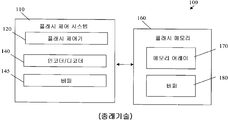
도 1은 종래 플래시 메모리 시스템의 개략적 블록도이다.
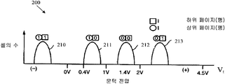
도 2는 도 1의 예시적 플래시 메모리에 대한 예시적인 문턱 전압 분포를 도시한다.
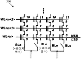
도 3은 MLC 플래시 메모리 장치에서의 예시적인 플래시 셀 어레이의 아키텍처를 도시한다.
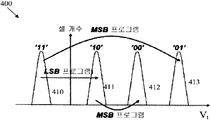
도 4는 도 2의 전압 할당 방식에 대한 예시적인 2 단계 MLC 프로그래밍 방식을 도시한다.
도 5a 및 5b는, 다 함께, 이웃 셀에 가해진 ICI를 감소시키는 다른 MLC 프로그래밍 방식을 도시한다.
도 6은 MLC 플래시 메모리 장치에서의 예시적인 플래시 셀 어레이를 더 자세히 도시한다.
도 7은 다수의 예시적인 공격자 셀에 기인하여 타겟 셀에 존재하는 셀간 간섭, 백 패턴 의존성, 잡음 및 기타 왜곡과 같은 외란을 도시한다.
도 8은 본 발명에 따라 제어기 기반 소프트 데이터 생성 기술을 포함하는 예시적인 플래시 메모리 시스템의 개략적 블록도이다.
도 9는 본 발명의 다른 실시형태에 따라 메모리 기반 소프트 데이터 생성 기술을 포함하는 예시적인 플래시 메모리 시스템의 개략적 블록도이다.
도 10은 본 발명에 따라 소프트 데이터 생성을 갖는 예시적인 플래시 메모리 시스템을 도시한다.
도 11은 본 발명의 특징을 포함하는 예시적인 소프트 데이터 생성 프로세스를 설명하는 흐름도이다.
도 12는 본 발명의 특징을 포함하는 소프트 데이터 생성 프로세스의 예시적인 다른 구현을 설명하는 흐름도이다.
도 13은 본 발명의 특징을 포함하는 예시적인 하드 데이터-소프트 데이터 매핑 데이터베이스로부터의 샘플 표이다. 1 is a schematic block diagram of a conventional flash memory system.
FIG. 2 illustrates an example threshold voltage distribution for the example flash memory of FIG. 1.
3 illustrates the architecture of an exemplary flash cell array in an MLC flash memory device.
4 illustrates an exemplary two-step MLC programming scheme for the voltage allocation scheme of FIG. 2.
5A and 5B together show another MLC programming scheme that reduces the ICI applied to neighboring cells.
6 illustrates an example flash cell array in more detail in an MLC flash memory device.
7 illustrates disturbances such as intercell interference, back pattern dependence, noise and other distortions present in the target cell due to many exemplary attacker cells.
8 is a schematic block diagram of an exemplary flash memory system including a controller based soft data generation technique in accordance with the present invention.
9 is a schematic block diagram of an exemplary flash memory system including a memory based soft data generation technique in accordance with another embodiment of the present invention.
10 illustrates an exemplary flash memory system with soft data generation in accordance with the present invention.
11 is a flow chart illustrating an exemplary soft data generation process incorporating features of the present invention.
12 is a flowchart illustrating another exemplary implementation of a soft data generation process incorporating features of the present invention.
13 is a sample table from an exemplary hard data-soft data mapping database incorporating features of the present invention.
본 발명의 다양한 태양은 단일 레벨 셀 또는 다중 레벨 셀(MLC) NAND 플래시 메모리 장치와 같은 메모리 장치에서의 개선된 디코딩을 위한 소프트 데이터 생성 기술에 관한 것이다. 본 명세서에서, 다중 레벨 셀 플래시 메모리는 각 메모리 셀이 2 이상의 비트를 저장하는 메모리를 포함한다. 통상, 하나의 플래시 셀에 저장된 다수의 비트는 상이한 페이지에 속한다. 본 발명이 여기서 아날로그 값을 전압으로 저장하는 메모리 셀을 이용하여 설명되지만, 본 발명은, 저장된 데이터를 나타내기 위해 전압, 전류 또는 저항을 사용하는 것과 같은 메모리 장치에 대한 여하한 저장 방식과 함게 사용될 수 있으며, 이는 당업자에게 명백할 것이다.Various aspects of the present invention relate to soft data generation techniques for improved decoding in memory devices such as single level cell or multi level cell (MLC) NAND flash memory devices. In the present specification, a multi-level cell flash memory includes a memory in which each memory cell stores two or more bits. Typically, multiple bits stored in one flash cell belong to different pages. Although the present invention is described herein using memory cells that store analog values as voltages, the present invention can be used with any storage scheme for memory devices, such as using voltage, current, or resistance to represent stored data. It will be apparent to those skilled in the art.
도 1은 종래의 플래시 메모리 시스템(100)의 개략 블록도이다. 도 1에 도시된 바와 같이, 예시적인 플래시 메모리 시스템(100)은 플래시 제어 시스템(110)과 플래시 메모리 블록(160)을 포함한다. 예시적인 플래시 제어 시스템(110)은 플래시 제어기(120), 인코더/디코더 블록(140) 및 하나 이상의 버퍼(145)를 포함한다. 다른 실시형태에서, 인코더/디코더 블록(140) 및 일부 버퍼(145)는 플래시 제어기(120) 내에서 내현될 수 있다. 인코더/디코더 블록(140) 및 버퍼(145)는, 예를 들어, 공지된 상용의 기술 및/또는 제품을 이용하여 구현될 수 있다.1 is a schematic block diagram of a conventional
예시적인 플래시 메모리 블록(160)은 메모리 어레이(170)와 하나 이상의 버퍼(180)를 포함할 수 있으며, 이들 각각은 공지된 사용의 기술 및/또는 제품을 이용하여 구현될 수 있다. 메모리 어레이(170)는, NAND 플래시 메모리, PCM(phase-change memory), MRM 메모리, NOR 플래시 메모리 또는 다른 비휘발성 플래시 메모리와 같은 단일 수준(single-level) 또는 다중 수준(multi-level) 셀 플래시 메모리로 구현될 수 있다. 본 발명이 주로 다중 수준 셀 NAND 플래시 메모리의 맥락에서 설명되지만, 본 발명은 단일 수준 셀 플래시 메모리 및 기타 비휘발성 메모리에도 적용될 수 있으며, 이는 당업자에게 명백할 것이다. Exemplary
다중 수준 셀 플래시 메모리Multi Level Cell Flash Memory
다중 수준 셀 NAND 플래시 메모리에서, 특정 셀과 관련된 전압 값을 사전 결정된 메모리 상태로 변환하는데 문턱 검출기가 통상 채용된다. 도 2는, 본 명세서에 참조로 포함되는 미국 특허 제6,522,580호의 개시 내용에 기초하여, 도 1의 예시적 다중 수준 셀 플래시 메모리(170)에 대한 예시적인 문턱 전압 분포를 도시한다. 일반적으로, 셀의 문턱 전압은 셀이 특정량의 전류를 도전시키기 위해 셀에 인가되어야 하는 전압이다. 문턱 전압은 셀에 저장된 데이터의 척도이다.In multilevel cell NAND flash memories, a threshold detector is typically employed to convert voltage values associated with a particular cell into a predetermined memory state. 2 illustrates an example threshold voltage distribution for the example multi-level
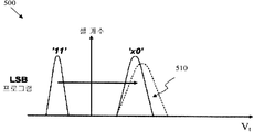
도 2에 도시된 예시적인 실시형태에서, 각 저장 소자는 각 메모리 셀에 2비트의 데이터를 저장하기 위해 4개의 가능한 데이터 상태를 사용한다. 도 2는 4개의 피크(210-213)를 도시하고, 각각의 피크는 하나의 상태에 대응한다. 다중 수준 셀 플래시 장치에서, 문턱 전압 분포 그래프(200)의 상이한 피크(210-213)는 셀에 2 비트를 저장하는데 사용된다.In the exemplary embodiment shown in FIG. 2, each storage element uses four possible data states to store two bits of data in each memory cell. 2 shows four peaks 210-213, each peak corresponding to one state. In a multilevel cell flash device, different peaks 210-213 of the threshold
문턱 전압 분포 그래프(200)의 피크(210-213)는 대응하는 이진 값으로 라벨링된다. 그러므로, 셀이 제1상태(210)에 있으면, 하위 비트(LSB(least significant bit)라고도 함)에 대한 "1"과 상위 비트(MSB(most significant bit)라고도 함)에 대한 "1"을 나타낸다. 상태(210)는 일반적으로 셀의 최초의 미프로그램(unprogrammed) 또는 소거 상태이다. 유사하게, 셀이 제2상태(211)에 있으면, 하위 비트에 대한 "0"과 상위 비트에 대한 "1"을 나타낸다. 셀이 제3상태(212)에 있으면, 하위 비트에 대한 "0"과 상위 비트에 대한 "0"을 나타낸다. 마지막으로, 셀이 제4상태(213)에 있으면, 하위 비트에 대한 "1"과 상위 비트에 대한 "0"을 나타낸다. Peaks 210-213 of threshold
문턱 전압 분포(210)는 0 볼트 아래의 음의 문턱 전압 수준을 갖는 소거 상태("11" 데이터 상태)에 있는 어레이 내의 셀의 문턱 전압 V1의 분포를 나타낸다. "10"과 "00" 사용자 데이터를 각각 저장하는 메모리 셀의 문턱 전압 분포(212 및 212)는 각각 0과 1 볼트 사이 및 1과 2 볼트 사이로 도시된다. 문턱 전압 분포(213)는 "01" 데이터 상태로 프로그램된 셀의 분포를 도시하며, 판독 패스 전압(read pass voltage)의 2와 4.5 볼트 사이로 설정된 문턱 전압 수준을 갖는다.
그러므로, 도 2의 예시적인 실시형태에서, 0 볼트, 1 볼트 및 2 볼트가 각 수준 또는 상태 사이의 전압 수준 문턱으로 사용될 수 있다. 전압 수준 문턱은 플래시 메모리(160)(예를 들어, 플래시 메모리(160)내의 감지 회로)에 의해 주어진 셀의 전압 수준 또는 상태를 결정하는데 사용된다. 플래시 메모리(160)는, 측정된 전압과 전압 수준 문턱의 비교에 기초하여 각 셀에 하나 이상의 비트를 할당할 것이고, 이는 플래시 제어 시스템(110)으로 하드 디시젼(hard decision)으로서 전송된다. 추가하여 또는 다르게는, 소프트 정보를 이용하는 구현에 있어서, 플래시 메모리(160)는 측정된 전압 또는 측정된 전압의 양자화된 버전을 소프트 정보로서 플래시 제어 시스템(110)에 전송할 수 있고, 이 경우 메모리 셀에 저장된 비트의 수보다 많은 비트가 측정된 전압을 나타내는데 사용된다. Therefore, in the exemplary embodiment of FIG. 2, 0 volts, 1 volt and 2 volts can be used as the voltage level threshold between each level or state. The voltage level threshold is used to determine the voltage level or state of a cell given by flash memory 160 (eg, sensing circuitry in flash memory 160). The
또한, 셀은 통상 공지의 프로그램/확인(Program/Verify) 기술을 이용하여 프로그램됨이 중요하라. 일반적으로, 프로그램/확인 사이클 동안, 플래시 메모리(160)는, 셀 트랜지스터에 전하를 저장하기 위해 최소 타겟 문턱 전압을 초과할 때까지 점진적으로 증가하는 전압을 인가한다. 예를 들어, 도 2의 예에서 '10' 데이터 상태를 프로그램할 때, 플래시 메모리(160)는 0.4V의 최소 타겟 문턱 전압을 초과할 때까지 셀 트랜지스터에 전하를 저장하도록 증가하는 전압을 점진적으로 인가할 수 있다.It is also important that the cell is normally programmed using known program / verify techniques. In general, during a program / verify cycle,
이후에 자세히 설명하는 바와 같이, 단일의 메모리 셀에 저장된 2 비트 각각은 상이한 페이지로부터 온 것이다. 달리 말하면, 각 메모리 셀에 저장된 2 비트 각각은 상이한 페이지 주소를 운반한다. 도 2에 도시된 오른쪽의 비트는 하위 페이지 주소가 입력될 때 액세스된다. 왼쪽 비트는 상위 페이지 주소가 입력될 때 액세스된다. As detailed below, each of the 2 bits stored in a single memory cell is from a different page. In other words, each of the two bits stored in each memory cell carries a different page address. The bits on the right shown in FIG. 2 are accessed when the lower page address is entered. The left bit is accessed when the upper page address is entered.
도 3은 MLC(multi-level cell) 플래시 메모리 장치(160)의 예시적 플래시 셀 어레이(300)의 아키텍쳐를 도시하는데, 여기서 각각의 예시적인 셀은 통상 2 비트를 저장하는 부동 게이트 트랜지스터에 대응한다. 도 3에서, 각 셀은 2개의 비트가 속하는 2 개의 페이지에 대한 2개의 숫자와 관련된다. 예시적인 셀 어레이 섹션(300)은 워드라인 n 내지 n+2 및 4개의 비트라인을 도시한다. 예시적인 플래시 셀 어레이(300)는 짝수 및 홀수 페이지로 분할되고, 여기서, 예를 들어, (번호 0 및 2를 갖는 셀과 같은) 짝수를 갖는 셀은 짝수 페이지에 대응하고, (번호 1 및 3을 갖는 셀과 같은) 홀수를 갖는 셀은 홀수 페이지에 대응한다. 워드라인 n은 예를 들어 짝수 비트라인의 짝수 페이지(0과 2)과, 홀수 비트라인의 홀수 페이지(1 및 3)을 저장한다. 3 illustrates the architecture of an example
또한, 도 3은 짝수나 홀수 비트라인 셀이 표시된 순서로 연속하여(아래에서 위로) 선택되고 프로그램되는 예시적인 프로그램 시퀀스를 나타낸다. 숫자는 페이지가 프로그램되는 순서를 나타낸다. 예를 들어, 페이지 0은 페이지 1 전에 프로그램된다. 짝수 및 홀수 페이지의 프로그래밍에 대한 추가적인 논의에 대해서는, 예를 들어, 본 명세서에 참조로 포함되는 K.-T. Park 등의 "A Zeroing Cell-to-Cell Interference Page Architecture with Temporary LSB Storing and Parallel MSB Program Scheme for MLC NAND Flash Memories," (IEEE Journal of Solid-State Circuits, Vol. 43, No. 4, 919-928 (2008 4월))을 참조하라. 3 also shows an example program sequence in which even or odd bitline cells are selected and programmed in succession (bottom to top) in the displayed order. The numbers indicate the order in which the pages are programmed. For example,
도 4는 도 2의 전압 할당 방식에 대한 예시적인 2단 MLC 프로그래밍 방식(400)을 도시한다. 도 4에 도시된 바와 같이, LSB 프로그램 단계 동안, 소거 상태(410)에 있는 선택된 셀의 상태는 LSB가 0이면 최저 프로그램 상태(411)로 이동한다. 그러므로, LSB 프로그래밍 단계에서, 메모리 셀은 소거 상태 '11'로부터 '10'으로 프로그램된다. 다음, MSB 프로그램 단계동안, 2개의 상태, 상태 '00'(412)와 '01'(413)가 이전 LSB 데이터에 따라 순차적으로 형성된다. 일반적으로, MSB 프로그래밍 단계동안, '10' 상태는 '00'으로 프로그램되고 상태 '11'은 '01'로 프로그램된다. 4 illustrates an exemplary two stage
도 4의 프로그래밍 방식(400)은 상태 410으로부터 상태 413으로의 상태 변화와 관련된 최대 전압 변이를 도시함을 유의하라. 상태 변화와 관련된 최대 전압 변이를 감소시켜 전압 변이에 의해 유발되는 ICI를 감소시키기 위해 많은 프로그래밍 방식이 제안 또는 제시되어왔다. Note that the
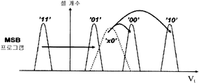
도 5a 및 5b는, 함께, 이웃 셀에 가해진 ICI를 감소시키는 다른 MLC 프로그래밍 방식(500)을 도시한다. 도 5a에 도시된 바와 같이, LSB 프로그래밍 단계 동안, 메모리 셀은 상태 '11'로부터 임시 (중간) 상태로서 'x0'로 SLC 프로그래밍과 유사한 방법으로 프로그램된다. 동일한 워드라인 내의 인접 셀도 LSB 프로그램된 후에, ICI에 의해 도 5a에서 피크(510)로 도시된 바와 같이 분포가 넓어질 수 있다. 그 후, 도 5b에 도시된 MSB 프로그래밍 단계에서, 'x0' 상태는 입력 데이터에 대응하는 최종 상태로서 '00'이나 '10'으로 프로그램되거나, 그렇지 않으면 '11' 상태가 최종 '01' 상태로 프로그램된다. 일반적으로, '11' 셀을 제외한 모든 메모리 셀은 MSB 프로그래밍 단계에서 LSB에 대한 임시 프로그램 상태로부터 그들의 최종 단계로 재 프로그램되어, 인접 셀에 의해 유발된 ICI가 많이 감소될 수 있다. 최종 상태의 셀은 중간 상태에 있을 때 겪었던 ICI를 겪지 않는데, 이는 셀이 최종 상태로 재 프로그램됐기 때문이다. 최종 상태의 셀은 최종 상태에 있은 이래로 겪은 ICI만을 격을 것이다. 상술한 바와 같이, 중간 프로그램 상태를 이용하는 도 5a 및 5b의 다단계 프로그래밍 시퀀스는 최대 전압 변화를 감소시키고, 그에 따라 이들 전압 변화에 의해 유발되는 ICI를 감소시킨다. 도 5b에서 예를 들어, MSB 프로그래밍 단계 동안 최대 전안 변이는 상태 '11' 에서 '01'로의 전이 및 상태 'x0'에서 '10'으로의 전이에 각각 관련된다는 것을 볼 수 있다. 이들 전압 변이는 도 4에서 상태 '11'로부터 '01'로의 최대 전압 변이보다 현저히 작다. 5A and 5B together show another
도 6은 MLC(multi-level cell) 플래시 메모리 장치(130) 내의 예시적인 플래시 셀 어레이(600)를 더 자세히 도시한다. 도 6에 도시된 바와 같이, 플래시 셀 어레이(600)는 플래시 셀, ci당 3 비트를 저장한다. 도 6은 한 블록에 대한 플래시 셀 어레이 아키텍쳐를 도시하는데, 여기서 각 예시적인 셀은 통상 3 비트를 저장하는 부동 게이트 트랜지스터에 대응한다. 예시적인 셀 어레이(600)는 m개의 워드라인과 n개의 비트라인으로 이루어진다. 통상, 현재의 다중 페이지(multi-page) 셀 플래시 메모리에서, 단일 셀 내의 비트는 서로 다른 페이지에 속한다. 도 6의 예에서, 각 셀에 대한 세 개의 비트는 세 개의 상이한 페이지에 대응하고, 각 워드라인은 3 페이지를 저장한다. 다음 논의에서, 페이지 0, 1 및 2는 워드라인 내의 하위, 중간 및 상위 페이지 수준이라고 지칭한다. 6 illustrates in more detail an exemplary
상술한 바와 같이, 플래시 셀 어레이는 짝수 및 홀수 페이지로 더 나눠질 수 있으며, 이 경우, 예를 들어, (도 6의 셀 2 및 4와 같은) 짝수를 갖는 셀은 짝수 페이지에 대응하고 (도 6의 셀 1 및 3과 같은) 홀수를 갖는 셀은 홀수 페이지에 대응한다. 이 경우에, (페이지 0과 같은) 페이지는 짝수 셀 내 짝수 페이지(짝수 페이지 0)을, 홀수 셀 내 홀수 페이지(홀수 페이지 0)을 포함할 것이다.As described above, the flash cell array can be further divided into even and odd pages, in which case, for example, cells with even numbers (such as
셀간 간섭 및 기타 외란Intercell Interference and Other Disturbance
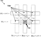
도 7은 다수의 예시적인 공격자 셀에 기인하여 타겟 셀에 존재하는 셀간 간섭, 백 패턴 의존성, 잡음 및 기타 왜곡과 같은 외란을 도시한다. 도 7에서 다음의 표기법이 사용된다.7 illustrates disturbances such as intercell interference, back pattern dependence, noise and other distortions present in the target cell due to many exemplary attacker cells. In Figure 7, the following notation is used.
WL: 워드라인;WL: word line;
BL: 비트라인;BL: bit line;
BLo: 홀수 비트라인;BLo: odd bitline;
BLe: 짝수 비트라인; 및BLe: Even Bitline; And
C: 커패시턴스.C: capacitance.
예를 들어, ICI가 타겟 셀(710)이 프로그램된 후에 프로그램되는 공격자 셀(720)에 의해 유발된다. ICI는 타겟 셀(710)의 전압 Vt를 변화시킨다. 예시적인 실시형태에서, "상향(bottom up)"프로그래밍 방식이 가정되고, 워드라인 i 및 i+1의 인접 공격자 셀이 타겟 셀(710)에 대해 ICI를 유발한다. 블록의 이러한 상향 프로그래밍으로, 하위 워드라인 i-1로부터의 ICI가 제거되고, 도 7에 도시된 바와 같이 5 개까지의 이웃 셀이 공격자 셀(720)로서 ICI에 기여한다. 그러나, 본 명세서에 개시된 기술은 워드라인 i-1과 같은 다른 워드라인으로부터의 공격자 셀이 ICI에 기여하는 경우로도 일반화될 수 있으며, 이는 당업자에게 명백할 것이다. 워드라인 i-1, i 및 i+1로부터의 공격자 셀이 ICI에 기여하는 경우, 8개까지의 최근접 이웃 셀이 고려되어야 한다. 타겟 셀로부터 더 먼 다른 셀은, 그들의 ICI에의 기여가 무시할 수 있다면, 무시될 수 있다. 일반적으로, 공격자 셀(720)은 프로그래밍 시퀀스 방식(상향 또는 홀수/짝수 기술 등)을 분석함으로써 식별되어 주어진 타겟 셀(710) 후에 프로그램되는 공격자 셀(720)을 식별한다.For example, ICI is caused by an
일반적으로, Vt는 셀 상에 저장된 데이터를 나타내는 전압이고 판독 동작 동안 획득된다. Vt는 판독 동작에 의해, 예를 들어, 셀 당 저장된 비트 수보다 더 높은 정확도의 소프트 전압 값으로서 또는 셀 당 저장된 비트 수(예를 들어, 3비트/셀 플래시에 대해 3비트)와 동일한 해상도를 갖는, 하드 전압 수준으로 양자화된 값으로 획득될 수 있다.In general, V t is the voltage representing the data stored on the cell and is obtained during a read operation. V t is the same resolution by a read operation, for example, as a soft voltage value with a higher accuracy than the number of bits stored per cell, or equal to the number of bits stored per cell (eg 3 bits per cell flash). Can be obtained as a value quantized to a hard voltage level.
ICI 감소 기술에 대한 추가적인 논의에 대해서는, 예를 들어, 각각 본 명세서에 참조로 포함되는, 명칭이 "Methods and Apparatus for Read-Side Intercell Interference Mitigation in Flash Memories"인 국제 특허 출원 PCT/US09/49326호, 또는 명칭이 ""Methods and Apparatus for Write-Side Intercell Interference Mitigation in Flash Memories"인 국제 특허 출원 PCT/US09/49327호를 참조하라. For further discussion of ICI reduction techniques, see, for example, International Patent Application PCT / US09 / 49326, entitled “Methods and Apparatus for Read-Side Intercell Interference Mitigation in Flash Memories,” each of which is incorporated herein by reference. Or International Patent Application PCT / US09 / 49327 entitled "Methods and Apparatus for Write-Side Intercell Interference Mitigation in Flash Memories."
도 8은 본 발명에 따른 제어기 기반 소프트 데이터 생성 기술을 포함하는 예시적인 플래시 메모리 시스템(800)의 개략적인 블록도이다. 도 8에 도시된 바와 같이, 예시적인 플래시 메모리 시스템(800)은 인터페이스(850)에 의해 연결된 플래시 메모리 블록(860)과 플래시 제어 시스템(810)을 포함한다. 예시적인 플래시 제어 시스템(810)은 통상 하나 이상의 집적 회로 상에 플래시 제어기(820)와 판독 채널(825)을 포함한다.8 is a schematic block diagram of an exemplary
예시적인 판독 채널(825)은 신호 처리 유니(830), 인코더/디코더 블록(840) 및 하나 이상 버퍼(845)를 포함한다. "판독 채널"이라는 용어는 기록 채널도 포함함을 유의하라. 다른 실시형태에서, 인코더/디코더 블록(840)및 일부 버퍼(845)는 플래시 제어기(820) 내에서 구현될 수 있다. 인코더/디코더 블록(840)과 버퍼(845)는, 예를 들어, 본 발명의 특징 및 기능을 제공하기 위해 본 명세서와 같이 변경한 공지된 상용의 기술 및/또는 제품을 이용하여 구현될 수 있다.
예시적인 신호 처리 유닛(830)은, 예를 들어, 각각 도 12a 및 12b와 관련하여 후술하는 하나 이상의 소프트 디매퍼 및/또는 소프트 데이터 생성 프로세스(835)를 구현하는 하나 이상의 프로세서를 포함한다. 예시적인 플래시 메모리 블록(860)은, 각각 공지된 상용의 기술 및/또는 제품을 이용하여 구현될 수 있는 메모리 어레이(870)와 하나 이상의 버퍼(880)를 포함한다. Exemplary
개시된 소프트 데이터 생성 기술의 다양한 실시형태에서, 예시적인 인터페이스(850)는 공격자 셀과 관련된 정보를 나타내는 값과 같은 종래의 플래시 메모리 시스템과 관련된 추가적인 정보를 운반하여야 할 수 있다. 그러므로, 인터페이스(850)는 종래 플래시 메모리 시스템의 인터페이스에 비해 더 큰 용량 또는 더 빠른 레이트를 가질 필요가 있을 수 있다. 인터페이스(850)는 선택적으로는 예를 들어, 명칭이 "Methods and Apparatus for Interfacing Between a Flash Memory Controller and a Flash Memory Array"이고 2009년 6월 30일에 출원되었으며 본 명세서에 참조로 포함되는 국제 특허 출원 PCT/US09/49328호(대리인 정리번호 08-0769)의 교시에 따라 구현될 수 있는데, 이는, 예를 들어, 더블 데이터 레이트(DDR) 기술을 이용하여 인터페이스(850)의 정보 운반 용량을 증가시킨다. 기록 동작 동안, 인터페이스(850)는 타겟 셀에 저장될 프로그램 값을 전달하는데, 통상 페이지 또는 워드라인 수준 액세스 기술을 이용한다. 예시적인 페이지 또는 워드라인 수준 액세스 기술에 대한 더 상세한 논의에 대해서는, 예를 들어, 본 명세서에 참조로 포함되는, 명칭이 "Methods and Apparatus for Storing Data in a Multi-Level Cell Flash Memory Device with Cross-Page Sectors, Multi-Page Coding and Per-Page Coding"인 2009년 3월 11일자로 출원된 국제 특허 출원 PCT/US09/36810호를 참조하라. In various embodiments of the disclosed soft data generation techniques,
판독 동작 동안, 인터페이스(850)는 타겟 셀 및 공격자 셀에 대해 메모리 어레이(870)로부터 획득된 하드 및/또는 소프트 판독 값을 전달한다. 예를 들어, 타겟 셀로 페이지에 대한 판독 값에 더하여, 상위/하위 워드라인 또는 인접한 짝수 또는 홀수 비트 라인의 하나 이상의 인접 페이지에 대한 판독 값이 인터페이스 버스를 통해 전달된다. 도 8의 실시형태에서, 개시된 소프트 데이터 생성 기술이 플래시 메모리 외부에서, 통상 최저 면적을 달성하기 위해 논리 회로를 위해 최적화된 처리 기술에서 구현된다. 그러나, 이는 인터페이스(850) 상에 전달될 수 있는 추가적인 공격 셀 데이터를 희생하게 된다.During the read operation, the
도 9는 본 발명의 다른 실시형태에 따른 메모리 기반 소프트 데이터 생성 기술을 포함하는 예시적인 플래시 메모리 시스템(900)의 개략적인 블록도이다. 도 9에 도시된 바와 같이, 예시적인 플래시 메모리 시스템(900)은 플래시 제어 시스템(910)과 플래시 메모리 블록(960)을 포함하고, 이들은 인터페이스(950)에 의해 연결된다.9 is a schematic block diagram of an exemplary
예시적인 플래시 제어 시스템(910)은 플래시 제어기(920)과 선택적인 판독 채널(925)을, 통상 하나 이상의 집적 회로 상에 포함한다. 다른 실시형태에서, 인코더/디코더 블록(940) 및 일부 버퍼(945)는 플래시 제어기(920) 내에 구현될 수 있다. 예시적인 플래시 제어기(920)는, 예를 들어, 본 발명의 특성 및 기능을 지원하도록 본 명세서에서와 같이 수정된, 공지된 상용의 기술 및/또는 제품을 이용하여 구현될 수 있다. 예시적인 판독 채널(925)은 인코더/디코더 블록(940)과 하나 이상의 버퍼(945)를 포함한다. 인코더/디코더 블록(940) 및 버퍼(945)는 공지된 상용의 기술 및/또는 제품을 이용하여 구현될 수 있다.Exemplary
예시적인 플래시 메모리 블록(960)은 메모리 어레이(970) 및 하나 이상의 버퍼(980)를 포함하며, 각각은 공지된 상용 기술 및/또는 제품을 이용하여 구현될 수 있다. 또한, 예시적 플래시 메모리 블록(960)은, 각각이 예를 들어 도 12a 및 12b와 관련하여 후술되는 하나 이상의 소프트 디매핑 및/또는 소프트 데이터 생성 프로세스(990)를 구현하는 하나 이상의 프로세서를 포함하는 예시적인 신호 처리 유닛(985)을 포함한다.Exemplary
개시된 소프트 데이터 생성 기술의 다양한 실시형태에서, 예시적인 인터페이스(950)는, 공격자 셀과 관련된 정보를 나타내는 값과 같은 종래의 플래시 메모리 시스템에 관한 추가적인 정보를 운반하여야 할 수 있다. 그러므로, 인터페이스(950)는 종래 플래시 메모리 시스템의 인터페이스에 비해 더 큰 용량 또는 더 빠른 레이트를 가질 필요가 있을 수 있다. 인터페이스(950)는 선택적으로는 예를 들어, 명칭이 "Methods and Apparatus for Interfacing Between a Flash Memory Controller and a Flash Memory Array"이고 2009년 6월 30일에 출원되었으며 본 명세서에 참조로 포함되는 국제 특허 출원 PCT/US09/49328호(대리인 정리번호 08-0769)의 교시에 따라 구현될 수 있는데, 이는, 예를 들어, 더블 데이터 레이트(DDR) 기술을 이용하여 인터페이스(950)의 정보 운반 용량을 증가시킨다.In various embodiments of the disclosed soft data generation techniques,
기록 동작 동안, 인터페이스(950)는 타겟 셀 및 공격 셀에 저장될 프로그램 데이터를 전달한다. 판독 동작 동안, 인터페이스(950)는 타겟 셀(들) 및 선택적으로는 공격자 셀에 대해 새로운 하드 또는 소프트 판독 값 또는 데이터를 전달한다. 통상, 단일 판독 액세스에 대해 운반되는 정보는 한 페이지 또는 워드라인의 데이터이다. 타겟 셀에 대한 데이터를 전송하는 것만이, 통상 논리 회로가 아니라 메모리에 최적화된 플래시 메모리를 제조하는데 사용되는 메모리 처리 기술을 이용하여 메모리 내에 소프트 데이터 생성 프로세스를 구현하는 것을 비용으로, 인터페이스(950)에 대한 대역폭 요구를 감소시킨다는 점을 유의하라.During a write operation, the
성능 조정에 기초한 소프트 데이터 생성Soft data generation based on performance tuning
이전에 언급한 바와 같이, 현재 플래시 메모리(860, 960)는 통상 디코딩을 위해 플래시 제어 시스템(810, 910)으로 하드 데이터를 제공하기만 한다. 그러나, 소프트 데이터가 디코딩 프로세스에서 에러 레이트 성능을 개선할 수 있다는 것이 잘 알려져 있다. 그러므로, 본 발명은 소프트 데이터를 추정 또는 강화하고 그에 의해 디코딩 성능을 개선하기 위해 플래시 메모리(860, 960)로부터의 하드 데이터를 사용하는 소프트 데이터 생성 기술을 제공한다.As previously mentioned,
본 발명의 일 태양에 따르면, 하드 데이터에 기초하여 플래시 메모리 장치(860, 960)와 같은 메모리 장치에 대해 소프트 데이터가 생성되고, 하나 이상의 성능 인자에 기초하여 조정(adjustment)가 생성된다. 본 명세서에서 사용되는 때에, 소프트 데이터는, 플래시 메모리 장치(860, 960)의 메모리 셀 내에 저장된 비트의 수보다 많은 수의 비트가 측정된 전압을 나타내는데 사용되는 경우 소프트 값을 포함하거나, 또는 메모리 셀 내에 저장된 비트의 신뢰도(reliability)를 나타내는 LLR을 포함한다. 하드 데이터는 메모리 셀 내에 저장된 (전압 수준과 같은) 수준 또는 (소프트 정보가 없는) 검출된 데이터 비트를 지칭하고, 이들은 플래시 메모리(870, 970)로부터 판독되고 종래의 플래시 메모리 장치에서 플래시 제어 시스템에 제공된다. In accordance with one aspect of the present invention, soft data is generated for a memory device, such as
예시적인 실시형태에 있어서, 소프트 데이터 값은, 플래시 메모리 블록(810, 910)에 의해 할당된 하드 데이터 값에 기초하는 공칭(nominal) 값과 플래시 메모리 블록(810, 910)의 성능에 영향을 주는 하나 이상의 인자를 보상하는 오프셋 값(또는 델타 값)의 합이다. 이 소프트 데이터 값은, 이후 LLR을 계산하는데 사용되는 (소프트 전압 값과 같은) 소프트 판독 값 또는 저장된 비트의 신뢰도를 나타내는 LLR 중 어느 하나이다. LLR의 생성 및 사용에 대한 더 자세한 논의에 대해서는, 예를 들어, 각각이 본 명세서에 참조로 포함되는, 명칭이 "Methods and Apparatus for Soft Demapping and Intercell Interference Mitigation in Flash Memories"이고 2009년 6월 30일에 출원된 국제 특허 출원 PCT/US09/49333 및 본 출원과 동일자로 출원된 명칭이 "Methods and Apparatus for Soft Data Generation in Flash Memories"인 국제 특허 출원을 참조하라. 소프트 데이터 생성기(835, 990)에 의해 생성된 LLR은 LPDC(Low Parity Density Check) 디코더와 같은 디코더에 제공된다. In an exemplary embodiment, the soft data values affect the performance of the flash memory blocks 810, 910 and nominal values based on the hard data values assigned by the flash memory blocks 810, 910. The sum of offset values (or delta values) that compensates for one or more factors. This soft data value is either a soft read value (such as a soft voltage value) that is then used to calculate the LLR or an LLR that represents the reliability of the stored bit. For a more detailed discussion of the generation and use of LLRs, see, for example, "Methods and Apparatus for Soft Demapping and Intercell Interference Mitigation in Flash Memories," each of which is incorporated herein by reference. See International Patent Application PCT / US09 / 49333, filed on May, and International Patent Application entitled "Methods and Apparatus for Soft Data Generation in Flash Memories" filed on the same date as this application. The LLRs generated by the
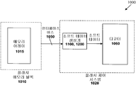
도 10은 예시적인 플래시 메모리 시스템(1000)의 개략적 블록도이다. 도 10은 본 발명의 소프트 데이터 생성 기술을 더 자세히 도시한다. 도 10에 도시된 바와 같이, 플래시 메모리 시스템(1000)은 인터페이스 버스(1050)에 의해 연결된, 플래시 제어 시스템(1020)과 플래시 메모리 블록(1010)을 포함한다. 10 is a schematic block diagram of an example
플래시 메모리 블록(1010)은 메모리 어레이(1015)에 포함된다. 플래시 메모리 블록(1010)은 메모리 어레이(1015)를 판독하고 판독되는 각 셀에 저장된 하드 데이터 값(즉, 하드 데이터 비트 또는 하드 전압 수준과 같은 하드 수준)을 결정한다. 이후에 논의되는 바와 같이, 하드 데이터 값은 통상 플래시 메모리 블록(1020)에 의해 할당되고, 추가의 디코딩 및 처리를 위해 인터페이스(1050)를 통해 플래시 제어기(1020)로 전달된다. The
예시적인 플래시 제어기(1020)는 도 11 및 12와 관련하여 후술하는 소프트 데이터 생성기(1100) 및 디코더(1060)를 포함한다. 일반적으로, 소프트 데이터 생성기(1100, 1200)는 플래시 메모리 블록(1020)에 의해 할당된 하드 데이터 값 및 하나 이상의 성능 인자 조정을 사용하여 소프트 데이터를 생성한다. 디코더(1060)는, 예를 들어, 신뢰 전파, 메시지 전달, 합-곱 또는 최소-합 알고리즘과 같은 LDPC 알고리즘을 사용하여 구현될 수 있다. 본 명세서에서 설명되는 소프트 데이터 생성기(1100, 1200)의 기능은 플래시 제어기(820), 판독 채널(825), 신호 처리 유닛(830) 및 디코더(840) 중 하나 이상에서 구현될 수 있음을 유의하라(예를 들어, 도 8 참조).Exemplary flash controller 1020 includes a
이전에 언급한 바와 같이, 본 발명의 일 태양은 하드 데이터와 추가 성능 인자의 함수로서 소프트 데이터를 계산한다. 일 예시적인 실시형태에서, 소프트 데이터 값은 플래시 메모리 블록(1010)에 의해 할당된 하드 데이터 수준에 기초한 공칭 값과 플래시 메모리 블록(1010)의 성능에 영향을 주는 하나 이상의 성능 인자를 보상하는 오프셋 값(또는 델타 값)의 합이다. As mentioned previously, one aspect of the present invention computes soft data as a function of hard data and additional performance factors. In one exemplary embodiment, the soft data value is a nominal value based on the hard data level assigned by the
예시적인 실시형태에서, 플래시 메모리 블록(1010)의 성능에 영향을 주는 성능 인자는, 인듀어런스(endurance)(예를 들어, 프로그램/소거 사이클의 수), 판독 사이클의 수, 리텐션(retention) 시간, 플래시 메모리의 온도 또는 온도 변화, 플래시 메모리를 제조하는데 사용되는 프로세스 코너, 셀간 간섭 영향 또는 다른 외란 메커니즘에 기인한 영향, 메모리 어레이 내의 위치 (워드라인 내 페이지 수준, 짝수 또는 홀수 비트라인 등) 및 공격자 셀에 저장된 데이터 패턴 중 하나 이상을 포함한다. 도 13과 관련하여 후술하는 바와 같이, 일 예시적 실시형태에서, 오프셋 값은 각각의 프로그램 수준에 대한 각각의 성능 인자에 대해 할당될 수 있다. 성능 열화를 보상하는 오프셋 값을 획득하기 위해, 성능 인자가 예를 들어 제조 테스트 동안에 미리 또는 간헐적이나 주기적으로 측정될 수 있다. 이들 성능 인자는 플래시 제어 시스템(810, 910)의 레지스터 또는 플래시 메모리(860, 960)에 저장되거나 프로그램될 수 있다. In an exemplary embodiment, performance factors affecting the performance of the
예를 들어, 소프트 데이터 값은 다음과 같이 계산될 수 있다.For example, the soft data value can be calculated as follows.

여기서 소프트 데이터 값은, 예를 들어, LLR을 나타내고 소프트 데이터 값의 부호는 하드 데이터 값을 나타내며 소프트 데이터 값의 크기(magnitude)는 신뢰도를 나타내고, nominal value0은 비트 0에 대한 최대 가능 신뢰도를 나타내는 양수이고, nominal value1은 비트 1에 대한 최대 가능 신뢰도를 나타내는 음수이며, offset은 플래시 메모리 블록(1010)의 성능에 영향을 주는 고려되는 성능 인자를 보상하는 총합(aggregate) 오프셋 값이다. 예를 들어, 0인 하드 데이터 값에 대해 nominal value0 은 +2이고, 1인 하드 데이터 값에 대해 nominal value1은 -2이다. 고려되는 성능 인자에 기초하여, 오프셋이 0보다 클 때 공칭 값의 크기는 감소된다. 달리 말하면, 소프트 데이터 값과 관련되는 신뢰도는 하드 데이터 값의 신뢰도를 감소시키는 성능 인자에 기초하여 감소된다.Here, the soft data value represents, for example, LLR, the sign of the soft data value represents the hard data value, the magnitude of the soft data value represents the reliability, and the nominal value 0 represents the maximum possible reliability for
통상, 소프트 데이터 값의 크기는 대응 하드 데이터 값의 신뢰도를 나타내고, 소프트 데이터 값의 부호는 대응 하드 데이터 값이 이진 0인지 1인지를 나타낸다. 예시적인 실시형태에서, 소프트 데이터 값은 -2과 +2 사이에서 변화할 수 있는데, 2는 최대 신뢰도를 갖는 이진 0의 값에 대응하고 -2는 최대 신뢰도를 갖는 이진 1의 값에 대응한다. 위의 식에서 채용된 오프셋 값은 플래시 메모리 장치의 신뢰도에 영향을 줄 외란을 특징화한다. 일반적으로, 오프셋 값은 예상되는 외란에 비례하여 변한다(예를 들어, 외란이 클수록 오프셋 값이 크다).Typically, the magnitude of the soft data value indicates the reliability of the corresponding hard data value, and the sign of the soft data value indicates whether the corresponding hard data value is binary zero or one. In an exemplary embodiment, the soft data value may vary between -2 and +2, where 2 corresponds to the value of binary zero with maximum confidence and -2 corresponds to the value of
일 예시적인 실시형태에서, 오프셋은 선택적으로 사전 규정된 값으로 포화(saturate)될 수 있다. 예를 들어, 오프셋이 플래시 메모리에 의해 할당된 비트에 대응하는 소프트 데이터 값의 부호를 변화시키지 않도록 보장하기 위해 오프셋이 포화될 수 있다.In one exemplary embodiment, the offset may optionally be saturated with a predefined value. For example, the offset may be saturated to ensure that the offset does not change the sign of the soft data value corresponding to the bit allocated by the flash memory.
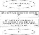
도 11은 본 발명의 특징을 포함하는 예시적인 소프트 데이터 생성 프로세스(1100)를 설명하는 흐름도이다. 일반적으로, 소프트 데이터 생성 프로세스(1100)는 하드 데이터 값을 소프트 데이터 값으로 직접, 예를 들어, 다양한 고려되는 성능 인자를 다루는 하드-소프트(hard-to-soft) 데이터 매핑 데이터베이스(1300)를 이용하여, 매핑함으로써 소프트 데이터 값을 생성한다.11 is a flow diagram illustrating an exemplary soft
도 11에 도시된 바와 같이, 소프트 데이터 생성 프로세스(1100)는 최초에 단계 1110 동안 플래시 메모리(1010)으로부터 하나 이상의 하드 데이터 값을 획득한다. 그 후, 단계 1120 동안, 소프트 데이터 생성 프로세스(1100)는 하나 이상의 하드 데이터 값에 기초하여 하나 이상의 소프트 데이터 값을 획득하고, 플래시 메모리(1010)의 하나 이상의 사전 규정된 성능 인자에 기초하여 하나 이상의 조정을 획득한다. 예를 들어, 소프트 데이터 생성 프로세스(1100)는 하드-소프트 도 13 데이터 매핑 데이터베이스(1300) 내에서 룩업(look-up)을 수행하기 위해 하드 데이터를 이용할 수 있다. 소프트 데이터 값은 후에 LLR을 계산하는데 사용되는 (소프트 전압 수준과 같은) 소프트 판독 값 또는 저장된 비트의 신뢰도를 나타내는 LLR 중 어느 하나를 나타낸다.As shown in FIG. 11, the soft
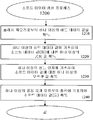
도 12는 본 발명의 특징을 포함하는 소프트 데이터 생성 프로세스(1200)의 예시적인 다른 구현을 설명하는 흐름도이다. 일반적으로, 소프트 데이터 생성 프로세스(1200)는, 플래시 메모리 블록(1010)에 의해 할당된 하드 데이터 값에 기초하는 공칭 값과 플래시 메모리 블록(1010)의 성능에 영향을 주는 하나 이상의 성능 인자를 보상하는 오프셋 값을 더함으로써 소프트 데이터 값을 생성한다. 소프트 데이터 값은 후에 LLR을 계산하는데 사용되는 (소프트 전압 수준과 같은) 소프트 판독 값 또는 저장된 비트의 신뢰도를 나타내는 LLR 중 어느 하나를 나타낸다. 12 is a flowchart illustrating another exemplary implementation of a soft
도 12에 도시된 바와 같이, 소프트 데이터 생성 프로세스(1200)는 최초에 단계 1210 동안 플래시 메모리(1010)으로부터 하나 이상의 하드 데이터 값을 획득한다. 그 후, 소프트 데이터 생성 프로세스(1200)는 단계 1220 동안 하나 이상의 하드 데이터 값에 기초하여 대응하는 하나 이상의 공칭 값을 획득하고, 단계 1230 동안 하나 이상의 고려되는 성능 인자에 기초하여 대응하는 하나 이상의 오프셋 값을 획득한다. 마지막으로, 단계 1240 동안 소프트 데이터 생성 프로세스(1200)는 획득된 하나 이상의 공칭 값과 오프셋 값의 총합(aggregation)에 기초하여 하나 이상의 희망 소프트 데이터 값을 획득한다. As shown in FIG. 12, the soft
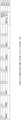
도 13은 플래시 메모리 셀 내에 LSB(least significant bit) 및 MSB(most significant bit)를 저장하는 예시적인 2비트/셀 MLC 플래시 메모리에 대한 본 발명의 특징을 포함하는 예시적인 하드 데이터-소프트 데이터(hard data-to-soft data) 매핑 데이터베이스(1300)로부터의 샘플 표이다. MLC 플래시 메모리 내 상이한 페이지 수준 (MSB와 LSB 페이지 등)은 다양한 성능 인자에 의해 상이하게 영향을 받으므로, 플래시 메모리 시스템의 에러 레이트 성능은 상이한 페이지 수준에 대해 별도의 오프셋을 사용함으로써 개선될 수 있다. 예시적인 하드 데이터-소프트 데이터 매핑 데이터베이스(1300)는 기록(1310)에 표시된 하드 데이터 값(예를 들어, 이진 1 또는 이진 0) 및 기록(1320)에 표시된 프로그램/소거 사이클의 수에 기초하여 기록(1330 및 1340)에 각각 LSB와 MSB에 대한 소프트 데이터를 기록한다. 이 예시적인 데이터베이스(1300)에서, 에러 레이트 성능을 개선하기 위해 이진 1 및 0에 대해 별도의 오프셋이 사용된다. 이진 1과 0에 대해 동일한 오프셋을 사용하고, 또한 MSB와 LSB 페이지와 같은 상이한 페이지 수준에 대해 동일한 오프셋을 사용하는 것은 에러 레이트 성능을 희생하여 데이터베이스의 복잡도를 감소시킬 수 있다. FIG. 13 illustrates exemplary hard data-soft data including features of the present invention for an exemplary 2-bit / cell MLC flash memory that stores a least significant bit (LSB) and a most significant bit (MSB) in a flash memory cell. data-to-soft data) is a sample table from the mapping database 1300. Since different page levels (such as MSB and LSB pages) in MLC flash memory are affected differently by various performance factors, the error rate performance of flash memory systems can be improved by using separate offsets for different page levels. . Exemplary hard data-soft data mapping database 1300 records based on the number of program / erase cycles indicated in
하드 데이터-소프트 데이터 매핑 데이터베이스(1300)는 짝수/홀수 비트 라인에 대한 오프셋 및/또는 메모리 어레이 내의 상이한 워드라인 위치와 같은 추가의 위치 특정(location-specific) 성능 인자 오프셋을 표시할 수도 있다. The hard data-soft data mapping database 1300 may indicate additional location-specific performance factor offsets, such as offsets for even / odd bit lines and / or different wordline locations in the memory array.
하드 데이터-소프트 데이터 매핑 데이터베이스(1300)는 위에서 논의한 예시적인 구현을 가정하되, 이진 0의 값은 +2로 매핑될 수 있고 이진 1의 값은 -2에 매핑될 수 있음을 유의하라. 패턴 의존성 및/또는, 판독 사이클 수, 프로세스 코너 및 온도 변화와 같은 추가적인 성능 인자를 설명하기 위해 예시적인 표(1300)는 선택적으로 다차원 표로 구현될 수 있음을 유의하라. The hard data-soft data mapping database 1300 assumes the example implementation discussed above, but note that the value of binary zero can be mapped to +2 and that the value of
패턴 의존 및 위치 특정 성능 인자의 더 상세한 논의에 대해서는, 예를 들어, 본 출원과 동일자로 출원되고 본 명세서에 참조로 포함되는 명칭이 "Methods and Apparatus for Soft Data Generation in Flash Memories" 국제 특허 출원을 참조하라.For a more detailed discussion of pattern dependence and location specific performance factors, see, for example, an international patent application entitled "Methods and Apparatus for Soft Data Generation in Flash Memories", filed on the same date as this application and incorporated by reference herein. See also.
프로그램/소거 사이클 및 인듀어런스를 설명하고 상이한 전압 수준에 대해 상이한 오프셋을 채용하는 도 4에 도시된 전압 분포에 대한 예시적인 구현을 고려하자. 또한, 이 구현에서, 성능 인자 오프셋은 통상-통상(TT; typical-typical), 고속-고속(FF;fast-fast) 및 저속-저속(SS; slow-slow)와 같은 복수의 상이한 프로세스 코너에 대해 특정된다. 이 예시적인 구현에서의 다음 성능 인자는, 예를 들어, 해당 성능 인자와 관련된 조건 하에서 플래시 메모리의 오프셋을 특징지우는 측정 또는 다른 제조 테스트에 기초할 수 있다:Consider an example implementation for the voltage distribution shown in FIG. 4 that describes program / erase cycles and endurance and employs different offsets for different voltage levels. Also, in this implementation, the performance factor offset may be in a plurality of different process corners, such as typical-typical (TT), fast-fast (FF) and slow-slow (SS). Is specified. The following performance factor in this example implementation may be based on, for example, a measurement or other manufacturing test that characterizes the offset of the flash memory under conditions associated with that performance factor:
(1) 인듀어런스 인자: 500 소거/프로그램 사이클 마다, 오프셋은 비트 라벨 '11'을 갖는 수준 0(410)에 대해 0.125, 비트 라벨 '10'을 갖는 수준 1(411) 및 비트 라벨 '01'을 갖는 수준 3(413)에 대해 0.375, 비트 라벨 '00'을 갖는 수준 2(412)에 대해 0.25. (1) Endurance factor: Every 500 erase / program cycles, the offset is 0.125 for level 0 (410) with bit label '11', level 1 (411) with bit label '10' and bit label '01'. 0.375 for
(2) 프로세스 코너 인자: 플래시 메모리가 제조되는 상이한 프로세스 코너에 대해 오프셋은, SS: 0.25 ; TT: 0; FF: 0.375.(2) process corner factor: for different process corners where the flash memory is manufactured, the offset is SS: 0.25; TT: 0; FF: 0.375.
그러므로, 500 소거/프로그램 사이클 후의 수준 1 및 SS 프로세스 코너에 대해, 소프트 데이터는 LSB(하드 데이터 비트=0)에 대해 2 - 0.375 - 0.25 = 1.375일 것이다. MSB 비트(하드 데이터 비트=1)에 대한 소프트 데이터는 -2 + 0.375 +0.25=-1.375일 것이다. 이 예시적인 실시형태에서, 셀에서 동일한 성능 인자 오프셋이 LSB와 MSB 양자 모두에 대해 사용된다. 상술한 바와 같이, 에러 레이트 성능을 더 개선하기 위해, LSB와 MSB 양자 모두에 대해 상이한 성능 인자 오프셋이 사용될 수 있다. Therefore, for
본 발명의 다른 태양에 따르면, 강화된 소프트 데이터 값이 플래시 메모리 장치에 의해 최초에 할당되는 소프트 데이터 값으로부터 생성된다. 강화된 소프트 데이터 값을 생성하기 위해 최초 소프트 데이터 값은 하나 이상의 고려되는 성능 인자에 기초하여 조정된다. 이들 강화된 소프트 데이터 값은 LLR 또는 신뢰도를 계산하는데 사용되는 (소프트 판독 전압과 같은) 소프트 판독 값을 나타내거나, LLR 또는 신뢰도를 나타낸다. According to another aspect of the present invention, an enhanced soft data value is generated from the soft data value initially assigned by the flash memory device. The initial soft data values are adjusted based on one or more of the considered performance factors to produce enhanced soft data values. These enhanced soft data values represent LLR or soft read values (such as soft read voltages) used to calculate reliability, or LLR or reliability.
일 예시적인 구현에서, 하나 이상의 소프트 판독 값이 플래시 메모리로부터 획득되고, LLR과 같은 소프트 정보가 소프트 판독 값에 기초하여 획득된다. 그 후, 소프트 소프트 정보(LLR 등)은 플래시 메모리의 하나 이상의 성능 인자에 기초하여 조정되어, 이후 에러 레이트 성능을 개선하기 위해 디코더로 전달되는 강화된 소프트 정보, 즉 강화된 소프트 데이터 값을 획득한다. In one exemplary implementation, one or more soft read values are obtained from flash memory, and soft information such as LLR is obtained based on the soft read values. The soft soft information (LLR, etc.) is then adjusted based on one or more performance factors of the flash memory to obtain enhanced soft information, i.e., enhanced soft data values, which are then passed to the decoder to improve error rate performance. .
다른 예시적인 구현에서, 하나 이상의 소프트 판독 값은 플래시 메모리로부터 획득된다. 대응하는 공칭 값은 그러면 소프트 판독 값에 기초하여 결정되고, 대응하는 오프셋 값은 하나 이상의 고려되는 성능 인자에 기초하여 획득된다. 그러면, LLR과 같은 희망 소프트 정보, 즉 소프트 데이터 값은 공칭 값 및 오프셋 값에 기초하여 획득된다. In another exemplary implementation, one or more soft read values are obtained from flash memory. The corresponding nominal value is then determined based on the soft read value, and the corresponding offset value is obtained based on one or more considered performance factors. Then, desired soft information such as LLR, that is, soft data value is obtained based on the nominal value and the offset value.
프로세스, 시스템 및 제품(Processes, systems and products ( articlearticle ofof manufacturemanufacture )의 상세 사항) Details
여기의 다수의 플로우 차트가 단계의 예시적인 순서를 설명하는 한편, 순서가 변할 수 있다는 것 또한 본원발명의 실시예이다. 알고리즘의 다양한 치환(permutations)은 본 발명의 다른 실시예로서 고려된다. 당업자가 자명하게 알 수 있듯이, 본원 발명의 예시적 실시예가 소프트웨어 프로그램 내 프로세싱 단계와 관련하여 설명되었지만, 다양한 기능이 소프트웨어 프로그램 내 프로세싱 단계로서의 디지탈 도메인 내에서, 회로 구성요소에 의한 하드웨어 내에서, 또는 스테이트 머신 또는 하드웨어와 소프트웨어 모두의 조합으로 구현될 수도 있다. 이러한 소프트웨어는, 예를 들어, 디시탈 신호 프로세서, 애플리케이션 특정 집적 회로, 마이크로 컨트롤러 또는 범용(general-purpose) 컴퓨터에서 사용될 수도 있다. 이러한 하드웨어와 소프트웨어는 집적 회로 내에 구현된 회로 내에서 구현될 수도 있다. While many of the flow charts herein illustrate an exemplary order of steps, it is also an embodiment of the present invention that the order may vary. Various permutations of the algorithm are contemplated as another embodiment of the present invention. As will be apparent to one skilled in the art, although exemplary embodiments of the present invention have been described in connection with processing steps in a software program, various functions may be performed in the digital domain as processing steps in the software program, in hardware by circuit components, or It may be implemented in a state machine or a combination of both hardware and software. Such software may be used, for example, in digital signal processors, application specific integrated circuits, microcontrollers or general-purpose computers. Such hardware and software may be implemented within circuitry implemented within integrated circuits.
그래서, 본원 발명의 기능은 이러한 방법의 실행을 위한 방법과 장치의 형태로 구현될 수 있다. 본원 발명의 하나 이상의 측면은, 예를 들어, 저장 매체에 저장되거나, 머신에 로딩되거나/되고 머신에 의해 실행되거나, 어떠한 전송 매체를 넘어 전송되는 프로그램 코드의 형태로 구현되고, 이 프로그램 코드가 컴퓨터와 같은 머신에 로딩되고 이에 의해 실행되는 경우, 그 머신은 본 발명을 실행하는 장치가 된다. 범용 프로세서에 구현된 경우, 프로그램 코드 세그먼트는 프로세서와 결합되어 특정 논리 회로와 유사하게 동작하는 장치를 제공한다. 본 발명은 또한 하나 이상의 집적 회로, 디지탈 신호 프로세서, 마이크로프로세서와 마이크로 컨트롤러의 형태로 구현될 수 있다. Thus, the functionality of the present invention may be implemented in the form of methods and apparatus for carrying out such a method. One or more aspects of the invention are embodied in the form of program code, for example, stored on a storage medium, loaded on a machine, and / or executed by a machine, or transmitted over any transmission medium, the program code being a computer When loaded into and executed by a machine, such a machine becomes an apparatus for implementing the invention. If implemented in a general-purpose processor, the program code segment may be combined with the processor to provide an apparatus that operates similar to a particular logic circuit. The invention may also be implemented in the form of one or more integrated circuits, digital signal processors, microprocessors and microcontrollers.
해당 분야에 알려진 바와 같이, 여기에 논의된 방법과 장치는 그 위에서 구현되는 컴퓨터 판독 가능한 코드 수단을 가지는 컴퓨터 판독 가능한 매체를 그 자체가 포함하는 제조 물품으로서 배포될 수도 있다. 컴퓨터 판독 가능한 프로그램 코드 수단은 컴퓨터 시스템과 결합하여 동작 가능하여 여기에 논의된 방법을 수행하거나 장치를 제조하기 위하여 모든 또는 일부의 단계를 수행할 수 있다. 컴퓨터 판독 가능한 매체는 기록 가능한 매체(예를 들어, 플로피 디스크, 하드 드라이브, 컴팩트 디스크, 메모리 카드, 반도체 장치, 칩, ASIC)일 수도 있고, 송신 매체(예를 들어, 광섬유, 월드와이드 웹, 케이블 또는 시간 분할 다중 접속, 코드 분할 다중 접속 또는 다른 무선 주파수 채널을 이용하는 무선 채널을 포함하는 네트워크)일 수도 있다. 컴퓨터 시스템으로 사용하는 데에 적절한 정보를 저장할 수 있는 공지되거나 개발된 임의의 매체가 사용될 수도 있다. 컴퓨터 판독 가능한 코드 수단은 컴퓨터가, 컴팩트 디스크의 표면 상의 높이 변화 또는 자기 매체의 자성 변화와 같은, 인스트력선과 데이터를 읽을 수 있게 하는 임의의 메카니즘이다. As known in the art, the methods and apparatus discussed herein may be distributed as an article of manufacture that itself includes a computer readable medium having computer readable code means implemented thereon. The computer readable program code means may be operable in conjunction with a computer system to perform all or some of the steps for carrying out the method or manufacturing the device discussed herein. Computer-readable media may be recordable media (eg, floppy disks, hard drives, compact discs, memory cards, semiconductor devices, chips, ASICs), and transmission media (eg, optical fibers, worldwide web, cables) Or a network including a radio channel using time division multiple access, code division multiple access, or another radio frequency channel). Any medium known or developed that can store information appropriate for use with a computer system may be used. Computer readable code means is any mechanism that allows a computer to read inline lines and data, such as changes in height on the surface of a compact disc or changes in magnetic properties of magnetic media.
여기에 설명된 컴퓨터 시스템과 서버는 각각 관련 프로세서를 구성하여 여기에 개시된 방법, 단계와, 기능을 구현할 메모리를 각각 포함한다. 메모리는 분산되어 있거나 로컬일 수 있고, 프로세스는 분산되어 있거나 하나(singular)일 수 있다. 메모리는, 전기적, 자기적 또는 광학적 메모리로서 또는 이들 또는 다른 타입의 저장 장치의 임의의 조합으로서 구현될 수 있다. 또한, "메모리"라는 용어는 관련 프로세서에 의해 접속되는 어드레스 가능한 공간 내 어드레스로부터 또는 어드레스로 판독되거나 기록될 수 있는 임의의 정보를 포함하기에 충분하도록 넓게 해석되어야 한다. 이러한 정의로, 네트워크 상 정보도 관련 프로세서가 네트워크로부터 정보를 검색할 수 있기 때문에 메모리 내에 있다. The computer system and server described herein each comprise an associated processor and each includes a memory for implementing the methods, steps, and functions disclosed herein. The memory may be distributed or local, and the process may be distributed or singular. The memory may be implemented as an electrical, magnetic or optical memory or any combination of these or other types of storage devices. In addition, the term “memory” should be construed broadly enough to include any information that can be read or written to or from an address in an addressable space connected by the associated processor. With this definition, information on the network is also in memory because the relevant processor can retrieve information from the network.
여기에 도시되고 설명된 실시예와 변형예는 단순히 본 발명의 원리를 설명하는 것이고 다양한 변형을 본 발명의 범위와 정신을 벗어나지 않고 당업자에 의해 구현할 수도 있다는 것을 알 수 있을 것이다. It will be appreciated that the embodiments and variations shown and described herein are merely illustrative of the principles of the invention and that various modifications may be made by those skilled in the art without departing from the scope and spirit of the invention.
Claims (20)
적어도 하나의 판독 값을 획득하는 단계와,
상기 획득된 적어도 하나의 판독 값에 기초하여 상기 소프트 데이터 값을 생성하고 상기 메모리 장치의 하나 이상의 성능 인자에 기초하여 조정(adjustment)을 생성하는 단계를 포함하는
소프트 데이터 값 생성 방법.
A method of generating at least one soft data value for a memory device, the method comprising:
Obtaining at least one reading,
Generating the soft data value based on the obtained at least one read value and generating an adjustment based on one or more performance factors of the memory device.
How to generate soft data values.
상기 조정은 상기 획득된 적어도 하나의 판독 값에 기초하여 공칭(nominal) 값을 조정하고, 상기 조정은 상기 메모리 장치의 하나 이상의 성능 인자에 기초하는 오프셋 값을 포함하는
소프트 데이터 값 생성 방법.
The method of claim 1,
The adjustment adjusts a nominal value based on the obtained at least one read value, the adjustment including an offset value based on one or more performance factors of the memory device.
How to generate soft data values.
상기 성능 인자는 인듀어런스(endurance), 프로그램/소거 사이클의 수, 판독 사이클의 수, 리텐션(retention) 시간, 온도, 온도 변화, 프로세스 코너, 셀간 간섭 영향, 메모리 어레이 내의 위치, 상기 판독 값이 획득되는 워드라인의 위치, 상기 판독 값이 획득되는 페이지의 위치, 상기 판독 값이 판독되는 워드라인 내의 페이지의 위치 및 공격자 셀의 패턴 중 하나 이상을 포함하는
소프트 데이터 값 생성 방법.
The method of claim 2,
The performance factors include endurance, number of program / erase cycles, number of read cycles, retention time, temperature, temperature change, process corners, inter-cell interference effects, location in the memory array, the readings obtained At least one of a position of a wordline to be read, a position of a page from which the read value is obtained, a position of a page within a wordline from which the read value is read, and a pattern of attacker cells
How to generate soft data values.
상기 조정은 셀 내 상이한 비트, 워드라인 내 상이한 페이지, 상이한 비트 라인, 상이한 하드 판독 데이터 값 중 하나 이상에 대한 별개의 성능 인자에 기초하는
소프트 데이터 값 생성 방법.
The method of claim 2,
The adjustment is based on separate performance factors for one or more of different bits in a cell, different pages in a wordline, different bit lines, different hard read data values.
How to generate soft data values.
상기 판독 값은 데이터 비트, 전압 수준, 전류 수준 및 저항 수준 중 하나 이상을 포함하는
소프트 데이터 값 생성 방법.
The method of claim 1,
The readout includes one or more of data bits, voltage levels, current levels, and resistance levels.
How to generate soft data values.
상기 판독 값은 소프트 데이터와 하드 데이터 중 하나 이상을 포함하는
소프트 데이터 값 생성 방법.
The method of claim 1,
The read value includes one or more of soft data and hard data.
How to generate soft data values.
상기 소프트 데이터 값은 (i) 하나 이상의 LLR(log likelihood ratio)을 생성하는데 사용되는 소프트 판독 값과 (ii) 하나 이상의 LLR 중 하나 이상을 포함하는
소프트 데이터 값 생성 방법.
The method of claim 1,
The soft data value includes one or more of (i) a soft readout value used to generate one or more log likelihood ratios (LLRs) and (ii) one or more LLRs.
How to generate soft data values.
상기 소프트 데이터 값은 상기 적어도 하나의 판독 값의 신뢰도(reliability)를 나타내는
소프트 데이터 값 생성 방법.
The method of claim 1,
The soft data value is indicative of the reliability of the at least one read value.
How to generate soft data values.
상기 단계 중 하나 이상은 제어기, 판독 채널, 신호 처리 유닛 및 디코더 중 하나 이상에 의해 구현되는
소프트 데이터 값 생성 방법.
The method of claim 1,
One or more of the steps may be implemented by one or more of a controller, read channel, signal processing unit and decoder.
How to generate soft data values.
상기 조정은 미리 획득되고 메모리에 저장되는
소프트 데이터 값 생성 방법.
The method of claim 1,
The adjustment is obtained in advance and stored in memory
How to generate soft data values.
상기 조정을 측정하는 단계를 더 포함하는
소프트 데이터 값 생성 방법.
The method of claim 1,
Further comprising measuring the adjustment
How to generate soft data values.
상기 성능 인자는 하나 이상의 패턴 의존 성능 인자를 포함하는
소프트 데이터 값 생성 방법.
The method of claim 1,
The performance factor includes one or more pattern dependent performance factors.
How to generate soft data values.
상기 성능 인자는 하나 이상의 위치 특정(location-specific) 성능 인자를 포함하는
소프트 데이터 값 생성 방법.
The method of claim 1,
The performance factor includes one or more location-specific performance factors.
How to generate soft data values.
상기 메모리 장치는 플래시 메모리 장치인
소프트 데이터 값 생성 방법.
The method of claim 1,
The memory device is a flash memory device
How to generate soft data values.
상기 조정은 상기 판독 값의 신뢰도 값을 감소시키는
소프트 데이터 값 생성 방법.
The method of claim 1,
The adjustment reduces the confidence value of the read value.
How to generate soft data values.
상기 조정은 상기 공칭 값의 신뢰도 값을 상기 오프셋 값과 동일한 양만큼 감소시키는
소프트 데이터 값 생성 방법.
The method of claim 2,
The adjustment reduces the confidence value of the nominal value by an amount equal to the offset value.
How to generate soft data values.
메모리와,
상기 메모리에 결합된 적어도 하나의 프로세서를 포함하고,
상기 프로세서는
적어도 하나의 판독 값을 획득하고,
상기 획득된 적어도 하나의 판독 값에 기초하여 상기 소프트 데이터 값을 생성하고 상기 메모리 장치의 하나 이상의 성능 인자에 기초하여 조정을 생성하도록 동작하는
소프트 데이터 값 생성 시스템.
A system for generating at least one soft data value for a memory device, the system comprising:
A memory,
At least one processor coupled to the memory,
The processor is
Obtain at least one reading,
Generate the soft data value based on the obtained at least one read value and generate an adjustment based on one or more performance factors of the memory device.
Soft data value generation system.
상기 조정은 상기 획득된 적어도 하나의 판독 값에 기초하여 공칭(nominal) 값을 조정하고, 상기 조정은 상기 메모리 장치의 하나 이상의 성능 인자에 기초하는 오프셋 값을 포함하는
소프트 데이터 값 생성 시스템.
The method of claim 17,
The adjustment adjusts a nominal value based on the obtained at least one read value, the adjustment including an offset value based on one or more performance factors of the memory device.
Soft data value generation system.
상기 성능 인자는 인듀어런스(endurance), 프로그램/소거 사이클의 수, 판독 사이클의 수, 리텐션(retention) 시간, 온도, 온도 변화, 프로세스 코너, 셀간 간섭 영향, 메모리 어레이 내의 위치, 상기 판독 값이 획득되는 워드라인의 위치, 상기 판독 값이 획득되는 페이지의 위치, 상기 판독 값이 판독되는 워드라인 내의 페이지의 위치 및 공격자 셀의 패턴 중 하나 이상을 포함하는
소프트 데이터 값 생성 시스템.
The method of claim 18,
The performance factors include endurance, number of program / erase cycles, number of read cycles, retention time, temperature, temperature change, process corners, inter-cell interference effects, location in the memory array, the readings obtained At least one of a position of a wordline to be read, a position of a page from which the read value is obtained, a position of a page within a wordline from which the read value is read, and a pattern of attacker cells
Soft data value generation system.
상기 소프트 데이터 값은 (i) 하나 이상의 LLR(log likelihood ratio)을 생성하는데 사용되는 소프트 판독 값과 (ii) 하나 이상의 LLR 중 하나 이상을 포함하는
소프트 데이터 값 생성 시스템.The method of claim 17,
The soft data value includes one or more of (i) a soft readout value used to generate one or more log likelihood ratios (LLRs) and (ii) one or more LLRs.
Soft data value generation system.
Applications Claiming Priority (4)
| Application Number | Priority Date | Filing Date | Title |
|---|---|---|---|
| US19475108P | 2008-09-30 | 2008-09-30 | |
| US61/194,751 | 2008-09-30 | ||
| PCT/US2009/049333 WO2010002948A1 (en) | 2008-07-01 | 2009-06-30 | Methods and apparatus for soft demapping and intercell interference mitigation in flash memories |
| WOPCT/US2009/049333 | 2009-06-30 |
Publications (1)
| Publication Number | Publication Date |
|---|---|
| KR20110061650A true KR20110061650A (en) | 2011-06-09 |
Family
ID=42073862
Family Applications (3)
| Application Number | Title | Priority Date | Filing Date |
|---|---|---|---|
| KR1020117009704A KR20110061649A (en) | 2008-09-30 | 2009-09-30 | Method and apparatus for soft data generation for memory devices using decoder performance feedback |
| KR1020117009695A KR101758192B1 (en) | 2008-09-30 | 2009-09-30 | Methods and apparatus for soft data generation for memory devices |
| KR1020117009708A KR20110061650A (en) | 2008-09-30 | 2009-09-30 | Methods and apparatus for soft data generation for memory devices based on performance factor adjustment |
Family Applications Before (2)
| Application Number | Title | Priority Date | Filing Date |
|---|---|---|---|
| KR1020117009704A KR20110061649A (en) | 2008-09-30 | 2009-09-30 | Method and apparatus for soft data generation for memory devices using decoder performance feedback |
| KR1020117009695A KR101758192B1 (en) | 2008-09-30 | 2009-09-30 | Methods and apparatus for soft data generation for memory devices |
Country Status (8)
| Country | Link |
|---|---|
| US (4) | US8892966B2 (en) |
| EP (4) | EP2340540A1 (en) |
| JP (4) | JP5535219B2 (en) |
| KR (3) | KR20110061649A (en) |
| CN (4) | CN102171767A (en) |
| IL (4) | IL211895A0 (en) |
| TW (4) | TW201019327A (en) |
| WO (4) | WO2010039874A1 (en) |
Cited By (3)
| Publication number | Priority date | Publication date | Assignee | Title |
|---|---|---|---|---|
| KR20140099196A (en) * | 2013-02-01 | 2014-08-11 | 엘에스아이 코포레이션 | Compensation loop for read voltage adaptation |
| KR20150121671A (en) * | 2014-04-21 | 2015-10-29 | 실리콘 모션 인코포레이티드 | Method, memory controller, and memory system for reading data stored in flash memory |
| KR20210145809A (en) * | 2019-05-02 | 2021-12-02 | 실리콘 스토리지 테크놀로지 인크 | Output Array Neuron Transformation and Calibration for Analog Neural Memory in Deep Learning Artificial Neural Networks |
Families Citing this family (108)
| Publication number | Priority date | Publication date | Assignee | Title |
|---|---|---|---|---|
| CN102132350B (en) * | 2008-07-01 | 2015-06-17 | Lsi公司 | Methods and apparatus for soft demapping and intercell interference mitigation in flash memories |
| US8611151B1 (en) | 2008-11-06 | 2013-12-17 | Marvell International Ltd. | Flash memory read performance |
| US8947929B1 (en) * | 2008-11-06 | 2015-02-03 | Marvell International Ltd. | Flash-based soft information generation |
| US8107306B2 (en) | 2009-03-27 | 2012-01-31 | Analog Devices, Inc. | Storage devices with soft processing |
| US8213236B1 (en) | 2009-04-21 | 2012-07-03 | Marvell International Ltd. | Flash memory |
| CN101923896A (en) * | 2009-06-12 | 2010-12-22 | 威刚科技(苏州)有限公司 | Electronic storage device and error correcting method thereof |
| US8392809B1 (en) * | 2009-10-16 | 2013-03-05 | Marvell International Ltd. | Log-likelihood-ratio (LLR) table calibration |
| US8510628B2 (en) * | 2009-11-12 | 2013-08-13 | Micron Technology, Inc. | Method and apparatuses for customizable error correction of memory |
| KR101678404B1 (en) * | 2010-02-25 | 2016-11-23 | 삼성전자주식회사 | MEMORY SYSTEM USING A PRIORI PROBABILITY Information AND DATA PROCESSING METHOD THEREOF |
| TWI437570B (en) * | 2010-03-10 | 2014-05-11 | Macronix Int Co Ltd | Multi-level cell programming speed improvement through program level exchange |
| US8504885B2 (en) | 2010-03-31 | 2013-08-06 | Lsi Corporation | Methods and apparatus for approximating a probability density function or distribution for a received value in communication or storage systems |
| US8429500B2 (en) | 2010-03-31 | 2013-04-23 | Lsi Corporation | Methods and apparatus for computing a probability value of a received value in communication or storage systems |
| US8775913B2 (en) | 2010-03-31 | 2014-07-08 | Lsi Corporation | Methods and apparatus for computing soft data or log likelihood ratios for received values in communication or storage systems |
| US8332728B2 (en) * | 2010-04-02 | 2012-12-11 | Skymedi Corporation | Method and apparatus of generating a soft value for a memory device |
| KR101678407B1 (en) * | 2010-05-10 | 2016-11-23 | 삼성전자주식회사 | Data storage device and program method thereof |
| US9531406B2 (en) | 2010-05-31 | 2016-12-27 | Globalfoundries Inc. | Decoding of LDPC code |
| US8819503B2 (en) | 2010-07-02 | 2014-08-26 | Stec, Inc. | Apparatus and method for determining an operating condition of a memory cell based on cycle information |
| US8737141B2 (en) | 2010-07-07 | 2014-05-27 | Stec, Inc. | Apparatus and method for determining an operating condition of a memory cell based on cycle information |
| US8756394B1 (en) | 2010-07-07 | 2014-06-17 | Marvell International Ltd. | Multi-dimension memory timing tuner |
| US8737136B2 (en) * | 2010-07-09 | 2014-05-27 | Stec, Inc. | Apparatus and method for determining a read level of a memory cell based on cycle information |
| US8499227B2 (en) * | 2010-09-23 | 2013-07-30 | Micron Technology, Inc. | Memory quality monitor based compensation method and apparatus |
| CN102436842B (en) * | 2010-09-29 | 2014-05-14 | 群联电子股份有限公司 | Memory storage device, memory controller and method for generating log likelihood ratio |
| US8848438B2 (en) | 2010-10-05 | 2014-09-30 | Stec, Inc. | Asymmetric log-likelihood ratio for MLC flash channel |
| US8549382B2 (en) | 2010-12-17 | 2013-10-01 | Intel Corporation | Storage drive with LDPC coding |
| US9898361B2 (en) | 2011-01-04 | 2018-02-20 | Seagate Technology Llc | Multi-tier detection and decoding in flash memories |
| US9086984B2 (en) * | 2011-01-04 | 2015-07-21 | Seagate Technology Llc | Detection and decoding in flash memories with selective binary and non-binary decoding |
| US9292377B2 (en) * | 2011-01-04 | 2016-03-22 | Seagate Technology Llc | Detection and decoding in flash memories using correlation of neighboring bits and probability based reliability values |
| US9106264B2 (en) | 2011-01-04 | 2015-08-11 | Lsi Corporation | Encoding and decoding in flash memories using convolutional-type low-density parity check codes |
| US9082480B2 (en) * | 2011-01-04 | 2015-07-14 | Seagate Technology Llc | Detection and decoding in flash memories with error correlations for a plurality of bits within a sliding window |
| KR101736337B1 (en) * | 2011-02-28 | 2017-05-30 | 삼성전자주식회사 | Nonvolatile memory device, controller for controlling the same, and operation method thereor |
| US9502117B2 (en) | 2011-03-14 | 2016-11-22 | Seagate Technology Llc | Cell-level statistics collection for detection and decoding in flash memories |
| US9047955B2 (en) | 2011-03-30 | 2015-06-02 | Stec, Inc. | Adjusting operating parameters for memory cells based on wordline address and cycle information |
| US8549380B2 (en) | 2011-07-01 | 2013-10-01 | Intel Corporation | Non-volatile memory error mitigation |
| KR101775660B1 (en) * | 2011-09-29 | 2017-09-07 | 삼성전자주식회사 | Method of reading memory cells with different threshold voltages without variation of word line voltage and nonvolatile memory device using the same |
| KR101919902B1 (en) * | 2011-10-18 | 2018-11-20 | 삼성전자 주식회사 | Method of reading data in memory device |
| US20140359381A1 (en) * | 2011-11-02 | 2014-12-04 | The University Of Tokyo | Memory controller and data storage device |
| US8811545B2 (en) * | 2011-11-08 | 2014-08-19 | Mitsubishi Electric Research Laboratories, Inc. | Method for reducing interference in OFDM wireless networks |
| CN102394113B (en) * | 2011-11-14 | 2014-06-18 | 清华大学 | Dynamic LDPC error correction code method for flash memory |
| US8644067B2 (en) * | 2011-11-30 | 2014-02-04 | Sandisk Technologies Inc. | Systems and methods of decoding data using soft bits at a non-binary decoder that uses probabilistic decoding |
| US8913437B2 (en) * | 2011-12-15 | 2014-12-16 | Marvell World Trade Ltd. | Inter-cell interference cancellation |
| US9117529B2 (en) * | 2011-12-23 | 2015-08-25 | Hgst Technologies Santa Ana, Inc. | Inter-cell interference algorithms for soft decoding of LDPC codes |
| US8943386B1 (en) * | 2012-02-16 | 2015-01-27 | Sk Hynix Memory Solutions Inc. | Generating soft read values which optimize dynamic range |
| US9195586B2 (en) | 2012-02-23 | 2015-11-24 | Hgst Technologies Santa Ana, Inc. | Determining bias information for offsetting operating variations in memory cells based on wordline address |
| US8943384B2 (en) * | 2012-04-12 | 2015-01-27 | Seagate Technology Llc | Using a soft decoder with hard data |
| US9256522B1 (en) * | 2012-04-19 | 2016-02-09 | Sk Hynix Memory Solutions Inc. | Method and system for generating soft-information after a single read in NAND flash using expected and measured values |
| KR102089570B1 (en) | 2012-06-04 | 2020-03-16 | 삼성전자주식회사 | Storage device and data processing method thereof |
| US8856615B1 (en) | 2012-06-11 | 2014-10-07 | Western Digital Technologies, Inc. | Data storage device tracking log-likelihood ratio for a decoder based on past performance |
| US9239754B2 (en) * | 2012-08-04 | 2016-01-19 | Seagate Technology Llc | Single read based soft-decision decoding of non-volatile memory |
| US8732537B2 (en) | 2012-08-06 | 2014-05-20 | Lsi Corporation | Method and system for symbol error rate estimation and sector quality measurement |
| RU2012134916A (en) * | 2012-08-15 | 2014-02-20 | ЭлЭсАй Корпорейшн | METHOD FOR SELECTING THE SUITABLE LDCP CODE |
| US9159407B2 (en) * | 2012-10-22 | 2015-10-13 | Apple Inc. | Soft readout from analog memory cells in the presence of read threshold errors |
| KR102005709B1 (en) * | 2012-10-22 | 2019-08-01 | 삼성전자 주식회사 | A method of operating the memory device and the memory system |
| KR102081581B1 (en) | 2012-11-02 | 2020-02-26 | 삼성전자 주식회사 | A method of operating the memory device |
| CN103811077B (en) * | 2012-11-12 | 2017-03-29 | 光宝电子(广州)有限公司 | Data compensation method in flash memory |
| US9135155B2 (en) | 2012-11-30 | 2015-09-15 | Sandisk Technologies Inc. | Storage and retrieval of shaped data |
| US9575683B2 (en) | 2012-11-30 | 2017-02-21 | Sandisk Technologies Llc | Processing shaped data |
| US9190174B2 (en) | 2012-11-30 | 2015-11-17 | Micron Technology, Inc. | Determining soft data from a hard read |
| US9116822B2 (en) | 2012-12-07 | 2015-08-25 | Micron Technology, Inc. | Stopping criteria for layered iterative error correction |
| US9021332B2 (en) | 2012-12-11 | 2015-04-28 | Seagate Technology Llc | Flash memory read error recovery with soft-decision decode |
| US20140169102A1 (en) * | 2012-12-19 | 2014-06-19 | Western Digital Technologies, Inc. | Log-likelihood ratio and lumped log-likelihood ratio generation for data storage systems |
| WO2014109756A1 (en) | 2013-01-11 | 2014-07-17 | Empire Technology Development Llc | Page allocation for flash memories |
| US9065483B2 (en) | 2013-01-21 | 2015-06-23 | Micron Technology, Inc. | Determining soft data using a classification code |
| US9229848B2 (en) | 2013-01-21 | 2016-01-05 | Micron Technology, Inc. | Determining soft data for fractional digit memory cells |
| JP6367562B2 (en) * | 2013-01-31 | 2018-08-01 | エルエスアイ コーポレーション | Detection and decoding in flash memory using selective binary and non-binary decoding |
| WO2014133490A1 (en) | 2013-02-27 | 2014-09-04 | Empire Technology Development Llc | Linear programming based decoding for memory devices |
| US10061640B1 (en) | 2013-03-12 | 2018-08-28 | Western Digital Technologies, Inc. | Soft-decision input generation for data storage systems |
| US9021331B2 (en) * | 2013-03-14 | 2015-04-28 | Seagate Technology Llc | Method and apparatus for generation of soft decision error correction code information |
| KR102081415B1 (en) | 2013-03-15 | 2020-02-25 | 삼성전자주식회사 | Method of optimizing llr used in nonvolatile memory device and method of correcting error in nonvolatile memory device |
| US9286155B1 (en) * | 2013-05-24 | 2016-03-15 | Marvell International Ltd. | Systems and methods for generating soft information in a flash device |
| GB2518632A (en) | 2013-09-26 | 2015-04-01 | Ibm | Estimation of level-thresholds for memory cells |
| US9201729B2 (en) | 2013-10-21 | 2015-12-01 | Seagate Technology, Llc | Systems and methods for soft data utilization in a solid state memory system |
| CN103594123B (en) * | 2013-11-28 | 2016-09-14 | 中国科学院微电子研究所 | Non-volatility memorizer and correcting and regulating method thereof |
| US9859925B2 (en) | 2013-12-13 | 2018-01-02 | Empire Technology Development Llc | Low-complexity flash memory data-encoding techniques using simplified belief propagation |
| US9798613B2 (en) * | 2013-12-27 | 2017-10-24 | Toshiba Memory Corporation | Controller of nonvolatile semiconductor memory |
| US9645763B2 (en) * | 2014-01-13 | 2017-05-09 | Seagate Technology Llc | Framework for balancing robustness and latency during collection of statistics from soft reads |
| TWI521529B (en) * | 2014-04-15 | 2016-02-11 | 群聯電子股份有限公司 | Decoding method, memory storage device and memory control circuit unit |
| US9460783B2 (en) | 2014-06-03 | 2016-10-04 | Micron Technology, Inc. | Determining soft data |
| CN105468471A (en) * | 2014-09-12 | 2016-04-06 | 光宝科技股份有限公司 | Solid state storage device and error correction method thereof |
| JP2016062463A (en) * | 2014-09-19 | 2016-04-25 | 株式会社東芝 | Memory system, error correction unit and error correction method |
| US9639420B2 (en) * | 2015-03-13 | 2017-05-02 | Micron Technology, Inc. | High performance memory controller |
| US10148293B2 (en) * | 2015-03-17 | 2018-12-04 | SK Hynix Inc. | Incremental LLR generation for flash memories |
| US9595317B2 (en) * | 2015-05-28 | 2017-03-14 | Sandisk Technologies Llc | Multi-state programming for non-volatile memory |
| US10204006B2 (en) | 2015-10-28 | 2019-02-12 | Avago Technologies International Sales Pte. Limited | Systems and methods for side data based soft data flash memory access |
| US9740559B2 (en) * | 2015-10-28 | 2017-08-22 | Avago Technologies General Ip (Singapore) Pte. Ltd. | Systems and methods for compaction based flash memory data recovery |
| US10108489B2 (en) | 2015-10-28 | 2018-10-23 | Avago Technologies General Ip (Singapore) Pte. Ltd. | Systems and methods for efficient soft data based flash memory data recovery |
| CN105427892B (en) * | 2015-11-23 | 2018-05-01 | 北京大学深圳研究生院 | A kind of non-homogeneous error correction method and phase change memory apparatus towards phase change memory |
| KR102459077B1 (en) * | 2016-01-12 | 2022-10-27 | 삼성전자주식회사 | Memory system using non-linear filtering shceme and read method thereof |
| US9984752B2 (en) * | 2016-03-14 | 2018-05-29 | Toshiba Memory Corporation | Memory system and data encoding and decoding method to mitigate inter-cell interference |
| US10289484B2 (en) * | 2016-09-16 | 2019-05-14 | Micron Technology, Inc. | Apparatuses and methods for generating probabilistic information with current integration sensing |
| US10158380B2 (en) * | 2016-12-06 | 2018-12-18 | Sandisk Technologies Llc | ECC and read adjustment based on dynamic memory error model estimation |
| JP2019053798A (en) | 2017-09-14 | 2019-04-04 | 東芝メモリ株式会社 | Semiconductor storage device |
| CN107705817B (en) * | 2017-09-22 | 2020-09-08 | 山东存储之翼电子科技有限公司 | Decoding method and device using flash memory channel characteristics and data storage system |
| TWI693604B (en) * | 2018-03-06 | 2020-05-11 | 深圳衡宇芯片科技有限公司 | Method and system for determining bit values in non-volatile memory |
| CN108563533A (en) * | 2018-03-27 | 2018-09-21 | 深圳忆联信息系统有限公司 | A method of it obtaining ICI impact factors and promotes error correcting capability |
| KR102653843B1 (en) * | 2018-04-19 | 2024-04-02 | 에스케이하이닉스 주식회사 | Data Storage Device and Operation Method for Preventing of Read Disturbance Thereof, Storage System Using the Same |
| CN110444242B (en) * | 2018-05-03 | 2023-09-08 | 爱思开海力士有限公司 | Memory system with deep learning based disturbance correction capability and method of operation |
| US11099781B2 (en) * | 2018-07-19 | 2021-08-24 | Silicon Motion, Inc. | Flash memory controller, flash memory module and associated electronic device |
| JP7066584B2 (en) | 2018-09-18 | 2022-05-13 | キオクシア株式会社 | Memory system |
| CN109379087B (en) * | 2018-10-24 | 2022-03-29 | 江苏华存电子科技有限公司 | Method for LDPC to modulate kernel coding and decoding rate according to error rate of flash memory component |
| US11349495B2 (en) * | 2020-04-15 | 2022-05-31 | Seagate Technology Llc | Recovering from hard decoding errors by remapping log likelihood ratio values read from NAND memory cells |
| US11177002B1 (en) * | 2020-06-30 | 2021-11-16 | Sandisk Technologies Llc | Programming memory cells using encoded TLC-fine |
| US11699498B2 (en) | 2020-12-04 | 2023-07-11 | Micron Technology, Inc. | Managing probabilistic data integrity scan intervals |
| US11609857B2 (en) | 2020-12-04 | 2023-03-21 | Micron Technology, Inc. | Identification and caching of frequent read disturb aggressors |
| US11467737B2 (en) * | 2020-12-04 | 2022-10-11 | Micron Technology, Inc. | Reducing probabilistic data integrity scan collisions |
| US11409599B2 (en) | 2020-12-04 | 2022-08-09 | Micron Technology, Inc. | Managing probabilistic data integrity scans in workloads with localized read patterns |
| KR20220080589A (en) * | 2020-12-07 | 2022-06-14 | 삼성전자주식회사 | Error Correcting Code Engine performing ECC decoding, operation method thereof, and Storage device including ECC engine |
| US20230229336A1 (en) * | 2022-01-20 | 2023-07-20 | Dell Products L.P. | Read-disturb-based read temperature time-based attenuation system |
| US11881869B1 (en) | 2022-09-30 | 2024-01-23 | SK Hynix Inc. | Asymmetric bit errors in low-density parity-check codes for non-volatile memory devices |
Family Cites Families (73)
| Publication number | Priority date | Publication date | Assignee | Title |
|---|---|---|---|---|
| US4015238A (en) * | 1975-11-24 | 1977-03-29 | Harris Corporation | Metric updater for maximum likelihood decoder |
| US5657332A (en) * | 1992-05-20 | 1997-08-12 | Sandisk Corporation | Soft errors handling in EEPROM devices |
| US6029264A (en) * | 1997-04-28 | 2000-02-22 | The Trustees Of Princeton University | System and method for error correcting a received data stream in a concatenated system |
| US6041430A (en) * | 1997-11-03 | 2000-03-21 | Sun Microsystems, Inc. | Error detection and correction code for data and check code fields |
| US5867429A (en) | 1997-11-19 | 1999-02-02 | Sandisk Corporation | High density non-volatile flash memory without adverse effects of electric field coupling between adjacent floating gates |
| US6560733B1 (en) * | 1999-07-09 | 2003-05-06 | Micron Technology, Inc. | Soft error detection for digital signal processors |
| JP3928311B2 (en) * | 1999-09-06 | 2007-06-13 | 三菱電機株式会社 | Turbo code error correction decoding apparatus and turbo code error correction decoding method |
| US6625236B1 (en) * | 2000-02-08 | 2003-09-23 | Ericsson Inc. | Methods and systems for decoding symbols by combining matched-filtered samples with hard symbol decisions |
| WO2001076079A2 (en) * | 2000-04-04 | 2001-10-11 | Comtech Telecommunication Corp. | Enhanced turbo product code decoder system |
| US7107511B2 (en) * | 2002-08-15 | 2006-09-12 | Broadcom Corporation | Low density parity check (LDPC) code decoder using min*, min**, max* or max** and their respective inverses |
| US6813322B2 (en) * | 2001-04-26 | 2004-11-02 | Telefonaktiebolaget L.M. Ericsson (Publ) | Soft output value biasing |
| JP3814502B2 (en) * | 2001-08-09 | 2006-08-30 | 松下電器産業株式会社 | Interference canceling apparatus and interference canceling method |
| JP2003152553A (en) * | 2001-11-13 | 2003-05-23 | Ntt Docomo Inc | Decoding method and communication apparatus |
| US7051264B2 (en) * | 2001-11-14 | 2006-05-23 | Monolithic System Technology, Inc. | Error correcting memory and method of operating same |
| JP3549519B2 (en) * | 2002-04-26 | 2004-08-04 | 沖電気工業株式会社 | Soft output decoder |
| US6751766B2 (en) * | 2002-05-20 | 2004-06-15 | Sandisk Corporation | Increasing the effectiveness of error correction codes and operating multi-level memory systems by using information about the quality of the stored data |
| KR100526186B1 (en) * | 2003-04-04 | 2005-11-03 | 삼성전자주식회사 | Method and apparatus for managing bad block in flash memory |
| US6980140B1 (en) * | 2004-06-18 | 2005-12-27 | Nortel Networks Limited | Flash ADC receiver with reduced errors |
| US7181676B2 (en) | 2004-07-19 | 2007-02-20 | Texas Instruments Incorporated | Layered decoding approach for low density parity check (LDPC) codes |
| CN100593911C (en) * | 2004-07-19 | 2010-03-10 | 德克萨斯仪器股份有限公司 | Method and system for decoding the layer data received by communication system |
| JP2006114078A (en) * | 2004-10-12 | 2006-04-27 | Toshiba Corp | Nonvolatile semiconductor memory device and operation method therefor |
| US7730384B2 (en) * | 2005-02-28 | 2010-06-01 | Agere Systems Inc. | Method and apparatus for evaluating performance of a read channel |
| US7187585B2 (en) | 2005-04-05 | 2007-03-06 | Sandisk Corporation | Read operation for non-volatile storage that includes compensation for coupling |
| US7276855B2 (en) * | 2005-07-15 | 2007-10-02 | General Electric Company | Auxilary lighting circuit for high intensity discharge system |
| JP4664797B2 (en) * | 2005-10-13 | 2011-04-06 | ジーイー・メディカル・システムズ・グローバル・テクノロジー・カンパニー・エルエルシー | MRI equipment |
| US7526715B2 (en) * | 2005-10-17 | 2009-04-28 | Ramot At Tel Aviv University Ltd. | Probabilistic error correction in multi-bit-per-cell flash memory |
| US7954037B2 (en) * | 2005-10-25 | 2011-05-31 | Sandisk Il Ltd | Method for recovering from errors in flash memory |
| WO2007062391A2 (en) * | 2005-11-22 | 2007-05-31 | Triton Systems, Inc. | Multilayer flame retardant barrier films and fabrics |
| JP2007183844A (en) * | 2006-01-10 | 2007-07-19 | Hitachi Global Storage Technologies Netherlands Bv | Auxiliary storage device and record reproduction method |
| US8055979B2 (en) * | 2006-01-20 | 2011-11-08 | Marvell World Trade Ltd. | Flash memory with coding and signal processing |
| US7844879B2 (en) * | 2006-01-20 | 2010-11-30 | Marvell World Trade Ltd. | Method and system for error correction in flash memory |
| US7400532B2 (en) | 2006-02-16 | 2008-07-15 | Micron Technology, Inc. | Programming method to reduce gate coupling interference for non-volatile memory |
| US7388781B2 (en) * | 2006-03-06 | 2008-06-17 | Sandisk Il Ltd. | Multi-bit-per-cell flash memory device with non-bijective mapping |
| US7502254B2 (en) * | 2006-04-11 | 2009-03-10 | Sandisk Il Ltd | Method for generating soft bits in flash memories |
| KR101375955B1 (en) | 2006-05-12 | 2014-03-18 | 애플 인크. | Distortion estimation and cancellation in memory devices |
| JP4999921B2 (en) * | 2006-05-12 | 2012-08-15 | アノビット テクノロジーズ リミテッド | Combination of distortion estimation and error correction coding for memory devices. |
| KR101202537B1 (en) * | 2006-05-12 | 2012-11-19 | 애플 인크. | Combined distortion estimation and error correction coding for memory devices |
| CN102306501B (en) | 2006-06-19 | 2014-03-19 | 桑迪士克股份有限公司 | Programming defferently sized margins and sensing with compensations at select states for improved read operations in non-volatile memory |
| JP4896605B2 (en) * | 2006-07-04 | 2012-03-14 | 株式会社東芝 | Nonvolatile semiconductor memory system |
| US7894269B2 (en) * | 2006-07-20 | 2011-02-22 | Sandisk Corporation | Nonvolatile memory and method for compensating during programming for perturbing charges of neighboring cells |
| WO2008019348A2 (en) | 2006-08-04 | 2008-02-14 | Metacarta, Inc. | Systems and methods for presenting results of geographic text searches |
| CA2660087C (en) * | 2006-08-05 | 2014-09-23 | Benhov Gmbh, Llc | Memory configuration and method for calibrating read/write data based on performance characteristics of the memory configuration |
| JP4791912B2 (en) | 2006-08-31 | 2011-10-12 | 株式会社東芝 | Nonvolatile semiconductor memory device and nonvolatile memory system |
| TWI353521B (en) | 2006-09-28 | 2011-12-01 | Sandisk Corp | Soft-input soft-output decoder for nonvolatile mem |
| JP5177991B2 (en) * | 2006-10-25 | 2013-04-10 | 株式会社東芝 | Nonvolatile semiconductor memory device |
| US7975192B2 (en) * | 2006-10-30 | 2011-07-05 | Anobit Technologies Ltd. | Reading memory cells using multiple thresholds |
| US7558109B2 (en) | 2006-11-03 | 2009-07-07 | Sandisk Corporation | Nonvolatile memory with variable read threshold |
| EP2084709B1 (en) | 2006-11-03 | 2014-04-02 | SanDisk Technologies Inc. | Nonvolatile memory with variable read threshold |
| KR100766042B1 (en) * | 2006-12-06 | 2007-10-12 | 삼성전자주식회사 | Multi-level cell memory device using concatenated coding |
| US7814401B2 (en) * | 2006-12-21 | 2010-10-12 | Ramot At Tel Aviv University Ltd. | Soft decoding of hard and soft bits read from a flash memory |
| US7480184B2 (en) * | 2007-01-07 | 2009-01-20 | International Business Machines Corporation | Maximum likelihood statistical method of operations for multi-bit semiconductor memory |
| US7966546B2 (en) * | 2007-03-31 | 2011-06-21 | Sandisk Technologies Inc. | Non-volatile memory with soft bit data transmission for error correction control |
| KR100838292B1 (en) * | 2007-06-20 | 2008-06-17 | 삼성전자주식회사 | Apparatus for controlling read level of memory cell and method using the same |
| KR101425958B1 (en) | 2007-09-06 | 2014-08-04 | 삼성전자주식회사 | Memory system capable of storing multi-bit data and its read method |
| US7751237B2 (en) * | 2007-09-25 | 2010-07-06 | Sandisk Il, Ltd. | Post-facto correction for cross coupling in a flash memory |
| US7656707B2 (en) * | 2007-12-14 | 2010-02-02 | Intel Corporation | Systems and methods for discrete channel decoding of LDPC codes for flash memory |
| KR101515122B1 (en) * | 2008-02-15 | 2015-04-27 | 삼성전자주식회사 | Memory data detecting apparatus and method for controlling reference voltage based on error of stored data |
| KR101437396B1 (en) * | 2008-02-27 | 2014-09-05 | 삼성전자주식회사 | Memory system comprising ecc block for reducing a latency and error correction method thereof |
| KR101378365B1 (en) * | 2008-03-12 | 2014-03-28 | 삼성전자주식회사 | Apparatus and method for hybrid detecting memory data |
| KR101398200B1 (en) | 2008-03-18 | 2014-05-26 | 삼성전자주식회사 | Memory device and encoding and/or decoding method |
| KR101398212B1 (en) | 2008-03-18 | 2014-05-26 | 삼성전자주식회사 | Memory device and encoding and/or decoding method |
| JP2009271852A (en) * | 2008-05-09 | 2009-11-19 | Toshiba Corp | Semiconductor storage device |
| US7843725B2 (en) | 2008-06-11 | 2010-11-30 | Micron Technology, Inc. | M+L bit read column architecture for M bit memory cells |
| US8464131B2 (en) * | 2008-06-23 | 2013-06-11 | Ramot At Tel Aviv University Ltd. | Reading a flash memory by constrained decoding |
| US8458563B2 (en) * | 2008-06-23 | 2013-06-04 | Ramot At Tel Aviv University Ltd. | Reading a flash memory by joint decoding and cell voltage distribution tracking |
| JP2010109468A (en) * | 2008-10-28 | 2010-05-13 | Toshiba Corp | Decoder, memory controller, and semiconductor memory device |
| JP4818381B2 (en) * | 2009-03-02 | 2011-11-16 | 株式会社東芝 | Semiconductor memory device |
| JP5361603B2 (en) * | 2009-08-13 | 2013-12-04 | 株式会社東芝 | controller |
| JP2011065599A (en) * | 2009-09-18 | 2011-03-31 | Toshiba Corp | Memory system and method of controlling the same |
| US8549385B2 (en) | 2009-12-15 | 2013-10-01 | Marvell World Trade Ltd. | Soft decoding for quantizied channel |
| US9245653B2 (en) | 2010-03-15 | 2016-01-26 | Intelligent Intellectual Property Holdings 2 Llc | Reduced level cell mode for non-volatile memory |
| US8498152B2 (en) | 2010-12-23 | 2013-07-30 | Sandisk Il Ltd. | Non-volatile memory and methods with soft-bit reads while reading hard bits with compensation for coupling |
| KR102149770B1 (en) | 2013-08-26 | 2020-08-31 | 삼성전자주식회사 | Memory controller and the method of operation thereof |
-
2009
- 2009-09-30 JP JP2011530195A patent/JP5535219B2/en not_active Expired - Fee Related
- 2009-09-30 JP JP2011530194A patent/JP5590620B2/en not_active Expired - Fee Related
- 2009-09-30 US US13/063,899 patent/US8892966B2/en not_active Expired - Fee Related
- 2009-09-30 EP EP09793198A patent/EP2340540A1/en not_active Withdrawn
- 2009-09-30 TW TW098133219A patent/TW201019327A/en unknown
- 2009-09-30 EP EP09793195.0A patent/EP2340538A1/en not_active Withdrawn
- 2009-09-30 CN CN2009801383272A patent/CN102171767A/en active Pending
- 2009-09-30 KR KR1020117009704A patent/KR20110061649A/en not_active Application Discontinuation
- 2009-09-30 TW TW098133247A patent/TWI581269B/en not_active IP Right Cessation
- 2009-09-30 TW TW098133217A patent/TWI517162B/en not_active IP Right Cessation
- 2009-09-30 EP EP09793200A patent/EP2340541A1/en not_active Withdrawn
- 2009-09-30 WO PCT/US2009/059087 patent/WO2010039874A1/en active Application Filing
- 2009-09-30 KR KR1020117009695A patent/KR101758192B1/en active IP Right Grant
- 2009-09-30 EP EP09793196A patent/EP2340539A1/en not_active Withdrawn
- 2009-09-30 CN CN200980143074.8A patent/CN102203875B/en active Active
- 2009-09-30 WO PCT/US2009/059069 patent/WO2010039859A1/en active Application Filing
- 2009-09-30 US US13/063,888 patent/US8830748B2/en active Active
- 2009-09-30 JP JP2011530196A patent/JP5535220B2/en not_active Expired - Fee Related
- 2009-09-30 KR KR1020117009708A patent/KR20110061650A/en not_active Application Discontinuation
- 2009-09-30 JP JP2011530193A patent/JP2012504820A/en active Pending
- 2009-09-30 CN CN200980143076.7A patent/CN102203876B/en active Active
- 2009-09-30 US US13/063,874 patent/US9064594B2/en not_active Expired - Fee Related
- 2009-09-30 WO PCT/US2009/059077 patent/WO2010039866A1/en active Application Filing
- 2009-09-30 US US13/063,895 patent/US9378835B2/en active Active
- 2009-09-30 WO PCT/US2009/059081 patent/WO2010039869A1/en active Application Filing
- 2009-09-30 CN CN200980143075.2A patent/CN102203877B/en not_active Expired - Fee Related
- 2009-09-30 TW TW098133227A patent/TWI562151B/en not_active IP Right Cessation
-
2011
- 2011-03-24 IL IL211895A patent/IL211895A0/en unknown
- 2011-03-27 IL IL211955A patent/IL211955A0/en unknown
- 2011-03-27 IL IL211956A patent/IL211956A0/en unknown
- 2011-03-28 IL IL211969A patent/IL211969A0/en unknown
Cited By (9)
| Publication number | Priority date | Publication date | Assignee | Title |
|---|---|---|---|---|
| KR20140099196A (en) * | 2013-02-01 | 2014-08-11 | 엘에스아이 코포레이션 | Compensation loop for read voltage adaptation |
| KR20150121671A (en) * | 2014-04-21 | 2015-10-29 | 실리콘 모션 인코포레이티드 | Method, memory controller, and memory system for reading data stored in flash memory |
| US9601219B2 (en) | 2014-04-21 | 2017-03-21 | Silicon Motion Inc. | Method, memory controller, and memory system for reading data stored in flash memory |
| US9959165B2 (en) | 2014-04-21 | 2018-05-01 | Silicon Motion Inc. | Method, memory controller, and memory system for reading data stored in flash memory |
| US10599516B2 (en) | 2014-04-21 | 2020-03-24 | Silicon Motion, Inc. | Method, memory controller, and memory system for reading data stored in flash memory |
| US11144390B2 (en) | 2014-04-21 | 2021-10-12 | Silicon Motion, Inc. | Method, memory controller, and memory system for reading data stored in flash memory |
| US11537469B2 (en) | 2014-04-21 | 2022-12-27 | Silicon Motion, Inc. | Method, memory controller, and memory system for reading data stored in flash memory |
| US11822428B2 (en) | 2014-04-21 | 2023-11-21 | Silicon Motion, Inc. | Method, memory controller, and memory system for reading data stored in flash memory |
| KR20210145809A (en) * | 2019-05-02 | 2021-12-02 | 실리콘 스토리지 테크놀로지 인크 | Output Array Neuron Transformation and Calibration for Analog Neural Memory in Deep Learning Artificial Neural Networks |
Also Published As
Similar Documents
| Publication | Publication Date | Title |
|---|---|---|
| US9064594B2 (en) | Methods and apparatus for soft data generation for memory devices based on performance factor adjustment | |
| US10929221B2 (en) | Multi-tier detection and decoding in flash memories utilizing data from additional pages or wordlines | |
| KR101671313B1 (en) | Methods and apparatus for read-side intercell interference mitigation in flash memories | |
| TWI596616B (en) | Inter-cell interference cancellation | |
| CN103843067B (en) | Read for dynamic on the piece of nonvolatile memory | |
| CN111052245B (en) | Determining data states of memory cells | |
| KR101662621B1 (en) | Methods and apparatus for programming multiple program values per signal level in flash memories | |
| KR101541710B1 (en) | Non-volatile memory and method for sensing with pipelined corrections for neighboring perturbations | |
| KR101526165B1 (en) | Non-volatile memory and method with continuous scanning time-domain sensing | |
| US20120069658A1 (en) | Methods, devices, and systems for dealing with threshold voltage change in memory devices | |
| US8677056B2 (en) | Methods and apparatus for interfacing between a flash memory controller and a flash memory array | |
| WO2013070368A1 (en) | Soft information generation for memory systems | |
| EP2537157A1 (en) | Non-volatile storage with temperature compensation based on neighbor state information | |
| US9007835B2 (en) | Enhanced data storage in 3-D memory using string-specific source-side biasing | |
| US9292377B2 (en) | Detection and decoding in flash memories using correlation of neighboring bits and probability based reliability values | |
| KR20110082016A (en) | Methods and apparatus for soft data generation for memory devices using reference cells |
Legal Events
| Date | Code | Title | Description |
|---|---|---|---|
| WITN | Application deemed withdrawn, e.g. because no request for examination was filed or no examination fee was paid |