KR20110030564A - Short thermal profile oven useful for screen printing - Google Patents
Short thermal profile oven useful for screen printing Download PDFInfo
- Publication number
- KR20110030564A KR20110030564A KR1020117000750A KR20117000750A KR20110030564A KR 20110030564 A KR20110030564 A KR 20110030564A KR 1020117000750 A KR1020117000750 A KR 1020117000750A KR 20117000750 A KR20117000750 A KR 20117000750A KR 20110030564 A KR20110030564 A KR 20110030564A
- Authority
- KR
- South Korea
- Prior art keywords
- substrate
- gas
- heat exchange
- conveyor
- substrate processing
- Prior art date
Links
Images


Classifications
-
- H—ELECTRICITY
- H01—ELECTRIC ELEMENTS
- H01L—SEMICONDUCTOR DEVICES NOT COVERED BY CLASS H10
- H01L21/00—Processes or apparatus adapted for the manufacture or treatment of semiconductor or solid state devices or of parts thereof
- H01L21/67—Apparatus specially adapted for handling semiconductor or electric solid state devices during manufacture or treatment thereof; Apparatus specially adapted for handling wafers during manufacture or treatment of semiconductor or electric solid state devices or components ; Apparatus not specifically provided for elsewhere
- H01L21/67005—Apparatus not specifically provided for elsewhere
- H01L21/67011—Apparatus for manufacture or treatment
- H01L21/67098—Apparatus for thermal treatment
- H01L21/67115—Apparatus for thermal treatment mainly by radiation
-
- H—ELECTRICITY
- H01—ELECTRIC ELEMENTS
- H01L—SEMICONDUCTOR DEVICES NOT COVERED BY CLASS H10
- H01L21/00—Processes or apparatus adapted for the manufacture or treatment of semiconductor or solid state devices or of parts thereof
- H01L21/67—Apparatus specially adapted for handling semiconductor or electric solid state devices during manufacture or treatment thereof; Apparatus specially adapted for handling wafers during manufacture or treatment of semiconductor or electric solid state devices or components ; Apparatus not specifically provided for elsewhere
- H01L21/67005—Apparatus not specifically provided for elsewhere
- H01L21/67011—Apparatus for manufacture or treatment
- H01L21/67098—Apparatus for thermal treatment
- H01L21/67109—Apparatus for thermal treatment mainly by convection
-
- H—ELECTRICITY
- H01—ELECTRIC ELEMENTS
- H01L—SEMICONDUCTOR DEVICES NOT COVERED BY CLASS H10
- H01L21/00—Processes or apparatus adapted for the manufacture or treatment of semiconductor or solid state devices or of parts thereof
- H01L21/67—Apparatus specially adapted for handling semiconductor or electric solid state devices during manufacture or treatment thereof; Apparatus specially adapted for handling wafers during manufacture or treatment of semiconductor or electric solid state devices or components ; Apparatus not specifically provided for elsewhere
- H01L21/67005—Apparatus not specifically provided for elsewhere
- H01L21/67242—Apparatus for monitoring, sorting or marking
- H01L21/67253—Process monitoring, e.g. flow or thickness monitoring
-
- H—ELECTRICITY
- H01—ELECTRIC ELEMENTS
- H01L—SEMICONDUCTOR DEVICES NOT COVERED BY CLASS H10
- H01L21/00—Processes or apparatus adapted for the manufacture or treatment of semiconductor or solid state devices or of parts thereof
- H01L21/67—Apparatus specially adapted for handling semiconductor or electric solid state devices during manufacture or treatment thereof; Apparatus specially adapted for handling wafers during manufacture or treatment of semiconductor or electric solid state devices or components ; Apparatus not specifically provided for elsewhere
- H01L21/677—Apparatus specially adapted for handling semiconductor or electric solid state devices during manufacture or treatment thereof; Apparatus specially adapted for handling wafers during manufacture or treatment of semiconductor or electric solid state devices or components ; Apparatus not specifically provided for elsewhere for conveying, e.g. between different workstations
- H01L21/67703—Apparatus specially adapted for handling semiconductor or electric solid state devices during manufacture or treatment thereof; Apparatus specially adapted for handling wafers during manufacture or treatment of semiconductor or electric solid state devices or components ; Apparatus not specifically provided for elsewhere for conveying, e.g. between different workstations between different workstations
- H01L21/67715—Changing the direction of the conveying path
-
- H—ELECTRICITY
- H01—ELECTRIC ELEMENTS
- H01L—SEMICONDUCTOR DEVICES NOT COVERED BY CLASS H10
- H01L21/00—Processes or apparatus adapted for the manufacture or treatment of semiconductor or solid state devices or of parts thereof
- H01L21/67—Apparatus specially adapted for handling semiconductor or electric solid state devices during manufacture or treatment thereof; Apparatus specially adapted for handling wafers during manufacture or treatment of semiconductor or electric solid state devices or components ; Apparatus not specifically provided for elsewhere
- H01L21/677—Apparatus specially adapted for handling semiconductor or electric solid state devices during manufacture or treatment thereof; Apparatus specially adapted for handling wafers during manufacture or treatment of semiconductor or electric solid state devices or components ; Apparatus not specifically provided for elsewhere for conveying, e.g. between different workstations
- H01L21/67703—Apparatus specially adapted for handling semiconductor or electric solid state devices during manufacture or treatment thereof; Apparatus specially adapted for handling wafers during manufacture or treatment of semiconductor or electric solid state devices or components ; Apparatus not specifically provided for elsewhere for conveying, e.g. between different workstations between different workstations
- H01L21/67718—Changing orientation of the substrate, e.g. from a horizontal position to a vertical position
-
- H—ELECTRICITY
- H01—ELECTRIC ELEMENTS
- H01L—SEMICONDUCTOR DEVICES NOT COVERED BY CLASS H10
- H01L21/00—Processes or apparatus adapted for the manufacture or treatment of semiconductor or solid state devices or of parts thereof
- H01L21/67—Apparatus specially adapted for handling semiconductor or electric solid state devices during manufacture or treatment thereof; Apparatus specially adapted for handling wafers during manufacture or treatment of semiconductor or electric solid state devices or components ; Apparatus not specifically provided for elsewhere
- H01L21/677—Apparatus specially adapted for handling semiconductor or electric solid state devices during manufacture or treatment thereof; Apparatus specially adapted for handling wafers during manufacture or treatment of semiconductor or electric solid state devices or components ; Apparatus not specifically provided for elsewhere for conveying, e.g. between different workstations
- H01L21/67739—Apparatus specially adapted for handling semiconductor or electric solid state devices during manufacture or treatment thereof; Apparatus specially adapted for handling wafers during manufacture or treatment of semiconductor or electric solid state devices or components ; Apparatus not specifically provided for elsewhere for conveying, e.g. between different workstations into and out of processing chamber
- H01L21/6776—Continuous loading and unloading into and out of a processing chamber, e.g. transporting belts within processing chambers
Abstract
본 발명은 기판 표면 상에 증착된 재료를 효과적으로 건조하기 위한 장치 및 방법을 제공한다. 본 발명에서 설명된 상기 장치 및 방법은 기판 표면 상에 증착된 재료로부터 용매 형태의 재료를 제거하는데 유용할 수 있다. 몇몇의 경우에 상기 재료는 스크린 인쇄 공정을 사용하여 증착될 수 있다. 일 실시예에서, 스크린 인쇄 챔버는 결정질 실리콘 기판 상에 패턴 재료를 증착한 후에 건조 챔버 내에서 증착 재료를 건조시키도록 구성된다. 일 실시예에서, 스크린 인쇄 챔버 및 건조 챔버는 미국 캘리포니아 산타 클라라 소재의 어플라이드 머티리얼즈 인코포레이티드 소유의 백시니 에스. 페. 아로부터 이용가능한 로터리 라인 툴 또는 소프트라인(등록상표) 툴 내에 모두 위치된다.The present invention provides an apparatus and method for effectively drying a material deposited on a substrate surface. The apparatus and methods described herein can be useful for removing material in solvent form from materials deposited on a substrate surface. In some cases the material may be deposited using a screen printing process. In one embodiment, the screen printing chamber is configured to dry the deposition material in the drying chamber after depositing the pattern material on the crystalline silicon substrate. In one embodiment, the screen printing chamber and drying chamber are fabricated from Applied Materials Inc., Santa Clara, California, USA. P. Both are located within the available rotary line tool or softline® tool.

Description
본 발명은 스크린 인쇄 공정과 같은 기판 표면 상에 패턴 층을 증착하는데 유용한 시스템에 관한 것이다.
The present invention relates to a system useful for depositing a pattern layer on a substrate surface, such as a screen printing process.
태양 전지는 태양광을 직접 전력으로 변환시키는 태양광발전(PV) 장치이다. PV 장치는 통상적으로, 하나 또는 그보다 많은 p-n 접합(p-n junction)을 가진다. 각각의 접합은 한쪽이 p-형 영역으로 지칭되고 다른 한쪽이 n-형 영역으로 지칭되는, 반도체 재료 내에 두 개의 상이한 영역을 포함한다. PV 전지의 p-n 접합이 (광자로부터의 에너지로 구성되는)태양광에 노출될 때, 태양광은 PV 효과를 통해 전력으로 직접적으로 변환된다. PV 태양 전지는 특정 양의 전력을 생성하며 태양 전지들은 소정 양의 시스템 전력을 분배할 수 있는 크기의 모듈로 타일처럼 구성된다. PV 모듈은 특정 프레임과 커넥터에 의해 패널로 접합된다. 태양 전지는 일반적으로, 단결정질 또는 다결정질 실리콘 기판 형태일 수 있는 실리콘 기판 상에 형성된다. 통상적인 PV 전지는 기판 내에 형성된 p-형 영역의 상부에 n-형 실리콘의 얇은 층을 갖는 두께 약 0.3 mm 미만인 p형 실리콘 웨이퍼, 기판 또는 시이트를 포함한다.Solar cells are photovoltaic (PV) devices that convert sunlight directly into power. PV devices typically have one or more p-n junctions. Each junction includes two different regions in the semiconductor material, one of which is referred to as a p-type region and the other of which is referred to as an n-type region. When the p-n junction of a PV cell is exposed to sunlight (consisting of energy from photons), the sunlight is converted directly to power through the PV effect. PV solar cells generate a certain amount of power, and the solar cells are configured like tiles in a module sized to distribute a certain amount of system power. PV modules are bonded to panels by specific frames and connectors. Solar cells are generally formed on a silicon substrate, which may be in the form of a monocrystalline or polycrystalline silicon substrate. Typical PV cells include p-type silicon wafers, substrates or sheets less than about 0.3 mm thick with a thin layer of n-type silicon on top of the p-type regions formed in the substrate.
태양광발전 시장은 지난 10년 동안 매년 30% 초과의 성장률로 성장해 왔다. 몇몇 학술지에는 전 세계적인 태양전지 발전량이 가까운 미래에 10 GWp를 초과할 것임을 암시하고 있다. 모든 태양광발전 모듈의 95% 이상이 실리콘 웨이퍼에 기반을 두게 될 것으로 추정하고 있다. 태양광발전 비용을 실질적으로 감소시켜야 할 필요성과 함께 높은 시장 성장률은 고 품질의 태양광발전 장치를 저렴하게 제조하기 위한 다수의 심각한 도전들을 초래했다. 그러므로, 상업적으로 생존 가능한 태양 전지를 제조함에 있어서의 하나의 주요한 요소는 장치의 수율을 개선함으로써 태양 전지를 제조하는데 요구되는 제작 비용을 감소시켜 장치를 제조하는데 소모되는 에너지의 감소 및/또는 기판 생산성을 증가시키는 것이다.The PV market has grown at a rate of over 30% annually for the past decade. Some journals suggest that global solar cell generation will exceed 10 GWp in the near future. It is estimated that over 95% of all PV modules will be based on silicon wafers. Along with the need to substantially reduce photovoltaic costs, high market growth has led to a number of serious challenges for the fabrication of high quality photovoltaic devices at low cost. Therefore, one major factor in the manufacture of commercially viable solar cells is to reduce the manufacturing costs required to manufacture solar cells by improving the yield of the device, thereby reducing the energy consumed to manufacture the device and / or substrate productivity. To increase.
스크린 인쇄는 천과 같은 대상물 상에 디자인을 인쇄하는데 오랫동안 사용되어 왔으며 기판의 표면 상에 전기 접점 및 상호접점과 같은 전기 구성요소의 디자인을 인쇄하기 위한 전자 산업에 사용되었다. 태양전지 제조 공정 분야에서도 스크린 인쇄공정을 사용한다.Screen printing has long been used to print designs on objects such as fabrics and in the electronics industry for printing designs of electrical components such as electrical contacts and interconnects on the surface of the substrate. The screen printing process is also used in the solar cell manufacturing process.
일반적으로, 구성 요소의 표면 상에 패턴을 증착한 후에 증착된 재료를 건조함으로써, 증착 패턴이 이후의 이송 단계 중에 안정화되고 태양전지 제조 중에 수행되는 고온 어닐링 공정과 같은 차후 처리 단계에 저항할 수 있게 하는 것이 바람직하다. 태양전지 제조 중에 사용된 종래의 복사 가열형 건조 공정은 기판에 의한 통상적인 근적외선(low infrared) 흡수로 인해 완료하는데 상당한 양의 시간과 상당한 양의 에너지 소모를 필요로 한다.In general, by depositing the pattern on the surface of the component and then drying the deposited material so that the deposition pattern is stabilized during subsequent transfer steps and resists subsequent processing steps such as high temperature annealing processes performed during solar cell manufacturing. It is desirable to. Conventional radiant heating drying processes used during solar cell fabrication require significant amounts of time and significant energy consumption to complete due to conventional low infrared absorption by the substrate.
또한, 용매 재료가 통상적으로, 건조 공정 중에 기판 표면 상에 증착된 재료로부터 제거되는데, 이는 건조 장치 내의 부품들 및 처리 기판들을 오염시킬 수 있다. 또한, 증착 재료로부터의 용매의 증발률 및 그에 따른 증착 재료를 건조하는데 요구되는 시간은 건조 장치의 처리 영역 내에 있는 용매 재료의 부분압에 의존할 수 있다. 그러므로, 기판과 지원 하드웨어의 오염을 감소시키기 위해 오븐 내의 증기량을 감소시키고 증발된 용매 재료를 제거하며 건조 공정 속도를 높이기 위한 방법이 필요하다.In addition, the solvent material is typically removed from the material deposited on the substrate surface during the drying process, which may contaminate the components and processing substrates in the drying apparatus. In addition, the evaporation rate of the solvent from the deposition material and thus the time required to dry the deposition material may depend on the partial pressure of the solvent material in the treatment region of the drying apparatus. Therefore, there is a need for a method to reduce the amount of vapor in the oven, remove evaporated solvent material, and speed up the drying process to reduce contamination of the substrate and supporting hardware.
그러므로, 스크린 인쇄 공정 중에 형성된 증착 재료를 건조하는데 소요되는 시간을 감소시키고 장치 수율을 개선하며 다른 공지의 장치들보다 낮은 소유비용(CoC)을 초래하는, 태양전지, 전자 회로 또는 다른 유용한 소자들을 제조하기 위한 스크린 인쇄 장치가 필요하다.
Therefore, manufacturing solar cells, electronic circuits or other useful devices that reduce the time spent drying the deposition material formed during the screen printing process, improve device yield and result in lower cost of ownership (CoC) than other known devices. There is a need for a screen printing apparatus.
본 발명은 일반적으로 기판 처리 장치를 제공하며, 상기 장치는 처리 영역을 통해 하나 또는 그보다 많은 기판을 이송하도록 구성되는 제 1 컨베이어와, 상기 제 1 컨베이어 상에 위치된 하나 또는 그보다 많은 기판으로 하나 또는 그보다 많은 파장에서 전자기 에너지를 분배하도록 구성되는 복사 열 전달 조립체, 및 내부에 배열되는 가열 소자를 갖는 플레넘, 및 상기 플레넘 내에 배열되는 상기 가열 소자를 지나치게 그리고 상기 처리 영역 내의 상기 제 1 컨베이어 상에 위치된 기판의 표면을 지나치게 가스를 이동시키도록 구성되는 유체 분배 장치를 포함하는 대류 열 전달 조립체를 포함한다.The present invention generally provides a substrate processing apparatus, the apparatus comprising: a first conveyor configured to transfer one or more substrates through a processing region and one or more substrates located on the first conveyor; A plenum having a radiant heat transfer assembly configured to distribute electromagnetic energy at more wavelengths, and a heating element arranged therein, and the heating element arranged in the plenum overlying and on the first conveyor in the processing region. And a convective heat transfer assembly comprising a fluid distribution device configured to move the gas excessively over the surface of the substrate located at.
본 발명의 실시예들은 기판 처리 방법을 더 제공하며, 상기 방법은 기판의 표면 상에 재료를 증착하는 단계와, 상기 재료의 증착 이후에 건조 챔버의 처리 영역으로 상기 기판을 이송하는 단계와, 상기 처리 영역 내에 위치된 상기 기판의 표면으로 상당한 양의 전자기 에너지를 분배하는 단계, 및 상기 처리 영역 내에 위치된 상기 기판의 표면을 지나치게 가열된 가스를 분배하는 단계를 포함한다.Embodiments of the present invention further provide a method of treating a substrate, the method comprising depositing material on a surface of a substrate, transferring the substrate to a processing region of a drying chamber after deposition of the material, and Distributing a significant amount of electromagnetic energy to the surface of the substrate located in the processing region, and distributing the overheated gas to the surface of the substrate located in the processing region.
본 발명의 실시예들은 기판 처리 방법을 더 제공하며, 상기 방법은 기판의 표면 상에 패턴 재료를 증착하는 단계와, 상기 패턴 재료를 증착한 이후에 컨베이어로 기판을 이송하는 단계와, 상기 컨베이어를 이용하여 건조 챔버의 처리 영역의 적어도 일부분을 통해 기판을 이송하는 단계와, 상기 처리 영역을 통해 기판이 이송될 때 기판의 표면으로 상당한 양의 전자기 에너지를 분배하는 단계, 및 기판이 상기 처리 영역을 통해 이송될 때 기판을 지나치게 가열된 가스를 분배하는 단계를 포함하며, 상기 가열된 가스를 분배하는 단계는 가열 소자를 지나치게 상기 가스를 유동시킴으로써 가스를 가열하는 단계와, 상기 처리 영역의 범위를 통과하도록 상기 가열된 가스를 지향시키는 단계, 및 상기 처리 영역을 통과하도록 지향된 상기 가열된 가스의 적어도 일부분을 수용하며, 상기 가열된 가스의 일부분을 재순환시키도록 상기 가열 소자를 지나치게 적어도 상기 가열된 가스의 일부분을 분배하는 단계를 더 포함한다.Embodiments of the present invention further provide a method for processing a substrate, the method comprising depositing a pattern material on a surface of a substrate, transferring the substrate to a conveyor after depositing the pattern material, and Transporting the substrate through at least a portion of the processing region of the drying chamber, distributing a significant amount of electromagnetic energy to the surface of the substrate as the substrate is transported through the processing region, and the substrate displacing the processing region. Distributing the heated gas over the substrate as it is conveyed, wherein dispensing the heated gas comprises heating the gas by flowing the gas excessively through a heating element and passing through a range of processing regions. Directing the heated gas so that it is suitable, and the product of the heated gas directed to pass through the processing region. Also accommodates a portion, further comprising the step of over-the heating elements distributed at least a portion of said heated gas so as to recycle a portion of the heated gas.
본 발명의 실시예들은 기판 처리 장치를 더 제공하며, 상기 장치는 처리 영역을 통해 하나 또는 그보다 많은 기판을 이송하도록 구성되는 제 1 컨베이어와, 상기 제 1 컨베이어 상에 위치된 하나 또는 그보다 많은 기판으로 하나 또는 그보다 많은 파장에서 전자기 에너지를 분배하도록 구성되는 복사 열 전달 조립체, 및 대류 열 전달 조립체를 포함하며, 상기 대류 열 전달 조립체는 복수의 열 교환 튜브 및 내부에 배열되는 가열 소자를 갖는 플레넘과, 상기 복수의 열 교환 튜브의 제 1 표면 및 상기 플레넘 내에 배열되는 가열 소자 전반에 걸쳐서 그리고 상기 처리 영역 내의 제 1 컨베이어 상에 위치되는 기판의 표면을 지나치게 가스를 이동시키도록 구성되는 유체 분배 장치와, 상기 복수의 열 교환 튜브의 온도를 제어하도록 구성되는 열 교환 장치, 및 상기 기판의 표면을 지나치게 이동된 가스를 수용하고 그 수용된 가스가 상기 열 교환 튜브의 제 2 표면을 지나치게 지향시키도록 위치되는 플레넘 입구를 포함한다.Embodiments of the present invention further provide a substrate processing apparatus, the apparatus comprising a first conveyor configured to transfer one or more substrates through a processing region and one or more substrates located on the first conveyor. A radiant heat transfer assembly configured to distribute electromagnetic energy at one or more wavelengths, and a convection heat transfer assembly, the convection heat transfer assembly comprising: a plenum having a plurality of heat exchange tubes and heating elements arranged therein; And a fluid distribution device configured to move gas excessively over a first surface of the plurality of heat exchange tubes and a heating element arranged in the plenum and over a surface of a substrate located on a first conveyor in the processing region. A heat exchange device configured to control a temperature of the plurality of heat exchange tubes, and A plenum inlet positioned to receive the gas that has been excessively moved over the surface of the substrate and the received gas to be too oriented to the second surface of the heat exchange tube.
본 발명의 실시예들은 기판 처리 방법을 더 제공하며, 상기 방법은 기판의 표면 상에 재료를 증착하는 단계와, 상기 재료의 증착 이후에 건조 챔버의 처리 영역으로 기판을 이송하는 단계와, 상기 처리 영역 내에 위치된 기판의 표면으로 상당한 양의 전자기 에너지를 분배하는 단계, 및 기판이 상기 처리 영역을 통해 이송될 때 기판으로 가열된 가스를 분배하는 단계를 포함하며, 상기 가열된 가스를 분배하는 단계는 가열 소자를 지나치게 상기 가스를 유동시킴으로써 가스를 가열하는 단계와, 상기 처리 영역 내에 위치된 기판을 지나치게 상기 가열된 가스를 지향시키는 단계와, 상기 기판을 지나치게 지향된 가열된 가스의 적어도 일부분을 수용하는 단계, 및 상기 가열된 가스로부터 에너지를 제거하기 위해 제 1 열 교환 표면으로 상기 가열된 가스를 분배하는 단계를 더 포함한다.Embodiments of the present invention further provide a method of treating a substrate, the method comprising depositing material on a surface of a substrate, transferring the substrate to a processing region of a drying chamber after deposition of the material, and treating the substrate. Distributing a significant amount of electromagnetic energy to the surface of the substrate located within the region, and distributing the heated gas to the substrate as the substrate is transported through the processing region, distributing the heated gas. Heating the gas by flowing the gas excessively through a heating element, directing the heated gas to a substrate located within the processing region, and receiving at least a portion of the heated gas too oriented the substrate; And the heated gas to a first heat exchange surface to remove energy from the heated gas. Further comprising the step of dispensing.
본 발명의 실시예들은 기판 처리 장치를 더 포함하며, 상기 장치는 제 1 회전 축선을 갖는 회전 작동기 조립체와, 상기 회전 작동기에 연결되는 제 1 기판 지지대와, 처리 영역을 통해 하나 또는 그보다 많은 기판을 이송시키고 상기 회전 작동기가 제 1 방위에 각위치될 때 상기 제 1 기판 지지대로부터 기판을 수용하도록 위치되는 제 1 컨베이어와, 제 2 컨베이어 상에 위치된 하나 또는 그보다 많은 기판으로 하나 또는 그보다 많은 파장에서 전자기 에너지를 분배하도록 구성되는 복사 열 전달 조립체, 및 대류 열 전달 조립체를 포함하며, 상기 대류 열 전달 조립체는 복수의 열 교환 튜브 및 내부에 배열되는 가열 소자를 갖는 플레넘과, 복수의 열 교환 튜브의 제 1 표면과 가열 소자 및 상기 처리 영역 내에 위치된 하나 또는 그보다 많은 기판 각각의 표면 전체에 걸쳐서 가스를 이동시키도록 구성되는 유체 분배 장치와, 상기 복수의 열 교환 튜브의 온도를 제어하도록 구성되는 열 교환 장치, 및 하나 또는 그보다 많은 기판의 표면을 지나치게 이동된 가스를 수용하고 상기 복수의 열 교환 튜브의 제 2 표면을 지나치게 수용된 상기 가스를 지향시키도록 위치되는 플레넘 입구를 포함한다.Embodiments of the present invention further comprise a substrate processing apparatus, the apparatus comprising a rotary actuator assembly having a first axis of rotation, a first substrate support coupled to the rotary actuator, and one or more substrates through a processing area. At one or more wavelengths with a first conveyor positioned to receive the substrate from the first substrate support when the rotary actuator is angularly positioned in the first orientation and one or more substrates positioned on the second conveyor. A radiant heat transfer assembly configured to distribute electromagnetic energy, and a convection heat transfer assembly, the convection heat transfer assembly comprising: a plenum having a plurality of heat exchange tubes and heating elements arranged therein; A table of each of the first surface and a heating element of the substrate and one or more substrates located within the processing region A fluid distribution device configured to move the gas throughout, a heat exchange device configured to control the temperature of the plurality of heat exchange tubes, and a surface of one or more substrates containing the gas that has been moved excessively and the plurality of A plenum inlet positioned to direct the second surface of the heat exchange tube of the gas to be excessively received.
본 발명의 전술한 특징들이 달성되고 더 상세히 이해될 수 있는 방식으로, 위에서 약술한 본 발명에 대해 첨부도면에 도시된 실시예들을 참조하여 상세히 설명될 것이다.
In the manner in which the foregoing features of the invention can be achieved and understood in more detail, the invention outlined above will be described in detail with reference to the embodiments shown in the accompanying drawings.
도 1은 본 발명의 일 실시예에 따른 스크린 인쇄 시스템의 등축도이며,
도 2는 본 발명의 일 실시예에 따른 도 1에 도시된 스크린 인쇄 시스템의 평면도이며,
도 3은 본 발명의 일 실시예에 따른 회전 작동기 조립체의 등축도이며,
도 4는 본 발명의 일 실시예에 따른 스크린 인쇄 시스템의 프린팅 네스트 부분(nest portion)의 등축도이며,
도 5는 본 발명의 일 실시예에 따른 건조 챔버의 측면 단면도이며,
도 6은 도 5에 따른 건조 챔버의 다른 측면 단면도이며,
도 7은 본 발명의 일 실시예에 따른 건조 챔버의 측면 횡단면도이다.1 is an isometric view of a screen printing system according to an embodiment of the present invention,
2 is a plan view of the screen printing system shown in FIG. 1 according to an embodiment of the present invention;
3 is an isometric view of a rotary actuator assembly according to one embodiment of the invention,
4 is an isometric view of a printing nest portion of a screen printing system according to one embodiment of the invention,
5 is a side cross-sectional view of a drying chamber according to an embodiment of the present invention,
6 is another side cross-sectional view of the drying chamber according to FIG. 5, FIG.
7 is a side cross-sectional view of a drying chamber according to an embodiment of the present invention.
이해를 촉진시키기 위해, 도면에서 공통인 동일한 구성요소를 지칭하기 위해 가능하다면, 동일한 참조 부호가 사용되었다. 일 실시예의 구성요소와 특징들은 추가의 언급없이도 다른 실시예에 유리하게 결합될 수 있다고 이해해야 한다.To facilitate understanding, the same reference numerals have been used where possible to refer to the same components that are common in the figures. It is to be understood that the components and features of one embodiment may be advantageously combined with other embodiments without further recitation.
그러나, 첨부 도면들은 본 발명의 단지 예시적인 실시예들만을 도시하며, 따라서 본 발명의 범주를 한정하는 것으로 이해해서는 안 되며 다른 균등한 효과적인 실시예들이 있을 수 있다고 이해해야 한다.However, the accompanying drawings show only exemplary embodiments of the invention, and therefore should not be understood as limiting the scope of the invention, but it should be understood that there may be other equivalent effective embodiments.
본 발명은 기판 표면 상에 증착된 재료를 효과적으로 건조하기 위한 장치 및 방법을 제공한다. 본 발명에서 설명되는 상기 장치 및 방법은 기판 표면에 증착된 재료로부터 용매 형태의 재료를 제거하는데 유용할 수 있다. 몇몇의 경우에 상기 재료들은 스크린 인쇄 공정을 사용하여 증착될 수 있다. 일 실시예에서, 스크린 인쇄 챔버는 결정질 실리콘 기판 상에 패턴 재료를 증착한 후에 건조 챔버 내에서 증착된 재료를 건조하도록 구성된다. 일 실시예에서, 스크린 인쇄 챔버 및 건조 챔버는 미국 캘리포니아 산타 클라라 소재의 어플라이드 소유인 Baccini S.p.A로부터 이용가능한 로터리 라인 툴 또는 소프트라인(등록상표) 툴 내에 모두 위치된다.The present invention provides an apparatus and method for effectively drying a material deposited on a substrate surface. The apparatus and methods described herein can be useful for removing material in solvent form from materials deposited on a substrate surface. In some cases the materials may be deposited using a screen printing process. In one embodiment, the screen printing chamber is configured to dry the deposited material in the drying chamber after depositing the pattern material on the crystalline silicon substrate. In one embodiment, the screen printing chamber and the drying chamber are both located in a rotary line tool or a softline® tool available from Baccini S.p.A, Applied in Santa Clara, California.
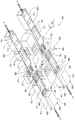
도 1 및 도 2는 본 발명의 다양한 실시예와 관련하여 사용될 수 있는 다중 스크린 프린팅 챔버 처리 시스템, 또는 시스템(100)을 도시한다. 일 실시예에서, 상기 시스템(100)은 일반적으로, 두 개의 유입 컨베이어(111), 회전 작동기 조립체(130), 두 개의 스크린 프린팅 헤드(102), 두 개의 유출 컨베이어(112) 및 두 개의 건조 챔버(200)를 포함한다. 두 개의 유입 컨베이어(111) 각각은 병렬식 처리 구성으로 구성됨으로써, 이들 컨베이어 각각은 인풋 컨베이어(113)와 같은 인풋 장치로부터 기판을 수용하며 그 기판을 회전 작동기 조립체(130)에 연결된 프린팅 네스트(131)로 이송한다. 또한, 유출 컨베이어(112) 각각은 회전 작동기 조립체(130)에 연결되는 프린팅 네스트(131)로부터 처리된 기판을 수용하며 처리된 각각의 기판을 건조 챔버(200)로 이송하도록 구성된다. 인풋 컨베이어(113) 및 건조 챔버(200) 내에 포함되는 건조기 컨베이어(114)는 일반적으로, 대형 제조 라인, 예를 들어 로터리 라인 툴 또는 소프트라인(등록상표) 툴에 연결되는, 즉 상기 시스템(100)에 연결되는 자동화 기판 취급 장치이다. 건조기 컨베이어(114), 유입 컨베이어(111), 유출 컨베이어(112), 및 인풋 컨베이어(113)가 벨트형 컨베이어로서 이후에 설명되지만, 다른 형태의 컨베이어, 로봇 장치, 또는 다른 유사한 기판 이송 기구들이 여기서 설명되는 본 발명의 기본 범주로부터의 변화없이 사용될 수 있다. 도 1 내지 도 4는 본 발명에서 설명된 다양한 실시예들로부터 유리한 하나의 가능한 처리 시스템의 구성만을 도시한 것이며, 따라서 다른 컨베이어 구성 및 다른 형태의 재료 증착 챔버가 여기서 설명된 본 발명의 기본 범주로부터 이탈함이 없이 사용될 수 있다는 것에 주목해야 한다.1 and 2 illustrate a multiple screen printing chamber processing system, or
도 2는 두 개의 프린팅 네스트(131)가 각각의 프린팅 네스트(131)로부터 유출 컨베이어(112)로 기판(150)을 이송하고 각각의 유입 컨베이어(111)로부터 기판(150)을 수용할 수 있도록 두 개의 프린팅 네스트(131)(예를 들어 참조 부호 "1" 및 "2")가 지향되어 있는 회전 작동기 조립체(130)의 위치를 개략적으로 도시하는 시스템(100)의 평면도이다. 따라서 기판 운동은 도 1 및 도 2에 도시된 통로"A"를 일반적으로 따른다. 이러한 구성에서, 다른 두 개의 프린팅 네스트(131)(예를 들어, 참조 부호 "2" 및 "4")는 스크린 인쇄 공정이 두 개의 스크린 인쇄 챔버(즉, 도 1의 스크린 인쇄 헤드(102)) 내에 위치된 기판(150) 상에서 수행될 수 있도록 지향된다. 또한, 이러한 구성에서 프린팅 네스트(131)는 네스트 상에서의 기판 운동의 방향이 회전 작동기 조립체(130)에 접선을 이루도록 지향된다. 회전 작동기 조립체(130)에 대한 컨베이어의 접선 방위는 상기 시스템의 차지 공간을 증가시킴이 없이 기판이 분배되고 두 위치, 예를 들어 참조 부호 "1" 및 "3"으로부터 수용될 수 있게 한다.2 shows that two printing
유입 컨베이어(111) 및 유출 컨베이어(112)는 일반적으로, 시스템 제어기(101)와 통신하는 작동기(도시 않음)의 사용에 의해 시스템(100) 내의 소정의 위치에 기판(150)을 지지하고 이송할 수 있는 적어도 하나의 벨트(116)를 포함한다. 도 1 및 도 2가 일반적으로 두 개의 벨트(116) 형태의 기판 이송 시스템을 도시하고 있지만, 본 발명의 기본 범주로부터의 변경없이 동일한 기판을 이송하고 위치시키는 기능(들)을 수행하기 위해 다른 형태의 이송 기구들이 사용될 수 있다.The
상기 시스템 제어기(101)는 일반적으로 전체 시스템(100)의 제어 및 자동화를 촉진하도록 설계되며 통상적으로 중앙 처리 유닛(CPU)(도시 않음), 메모리(도시 않음), 및 지원 회로(또는 I/O)(도시 않음)를 포함할 수 있다. 상기 CPU는 다양한 챔버 공정 및 하드웨어(예를 들어, 컨베이어, 검출기, 모터, 유체 분배 하드웨어 등)을 제어하고 상기 시스템 및 챔버 공정들(예를 들어, 기판 위치, 처리 시간, 검출기 신호 등)을 모니터링하기 위해 산업적 세팅 분야에 사용되는 임의 형태의 컴퓨터 프로세서 중의 하나의 형태일 수 있다. 상기 메모리는 CPU에 연결되며 랜덤 어쎄스 메모리(RAM), 읽기 전용 메모리(ROM), 플로피 디스크, 하드 디스크, 또는 로컬이나 원격 형태의 다른 디지털 스토리지와 같은 용이하게 이용가능한 메모리 중의 하나 또는 그보다 많은 메모리일 수 있다. 소프트웨어 지시어 및 데이타는 CPU를 지시하기 위해 메모리 내에 코드화되거나 저장될 수 있다. 상기 지원 회로도 종래 방식으로 프로세서를 지원하기 위해 CPU에 연결된다. 상기 지원 회로는 캐시(cache), 파워 서플라이, 클록 회로, 인풋/아웃풋 회로, 서브시스템 등을 포함할 수 있다. 시스템 제어기(101)에 의해 판독될 수 있는 프로그램(또는 컴퓨터 지시어)는 업무가 기판 상에서 수행 가능한지를 결정한다. 바람직하게, 상기 프로그램은 적어도 기판 위치 정보, 다양한 제어 요소들의 운동 시퀀스, 기판 검사 시스템 정보, 및 이들의 조합 정보를 생성 및 저장하기 위한 코드를 포함하는 시스템 제어기(101)에 의해 판독가능한 소프트웨어이다.The
상기 시스템(100)에 이용되는 두 개의 스크린 헤드(102)는 스크린 인쇄 공정 중에 프린팅 네스트(131) 상에 위치된 기판 표면 상에 소정의 패턴으로 재료를 증착하도록 구성되는, Baccini S.p.A로부터 이용가능한 종래의 스크린 프린팅 헤드일 수 있다. 일 실시예에서, 스크린 프린트 헤드(102)는 태양전지 기판 상에 금속 함유 또는 유전체 함유 재료를 증착하도록 구성된다. 일 예에서, 상기 기판은 약 125 mm 내지 156 mm 범위의 폭 및 약 70 mm 내지 156 mm 범위의 길이를 갖는 태양전지 기판이다.The two screen heads 102 used in the
일 실시예에서, 상기 시스템(100)은 또한 스크린 인쇄 공정의 수행 전후에 기판을 검사하도록 구성되는 검사 조립체(199)를 포함한다. 검사 조립체(199)는 도 1 및 도 2에 도시된 바와 같은 위치 "1" 및 "2"에 놓인 유입 또는 처리된 기판을 검사하도록 놓이는 하나 또는 그보다 많은 카메라(120)를 포함할 수 있다. 검사 조립체(199)는 일반적으로, 검사하고 그 검사결과를 시스템 제어기(101)와 통신함으로써 손상 또는 오처리된 기판이 제조 라인으로부터 제거될 수 있게 하는 적어도 하나의 카메라(120)(예를 들어, CCD 카메라) 및 다른 전자 구성요소들을 포함한다. 일 실시예에서, 프린팅 네스트(131)는 검사 조립체(199)에 의해 더욱 쉽게 검사될 수 있도록 지지대(138)(도 4)) 위에 놓인 기판(150)을 조사하기 위한 램프, 또는 다른 유사한 광학적 복사 장치를 각각 포함할 수 있다. 기판이 손상되었다면, 그 기판은 지지대(138) 내의 구성요소를 사용함으로써 폐기물 수집통(107)으로 이동될 수 있다.In one embodiment, the
검사 조립체(199)는 각각의 프린트 네스트(131) 상의 기판의 정밀한 위치를 결정하는데 사용될 수도 있다. 각각의 프린트 네스트(131) 상의 각각의 기판(150)에 대한 위치 데이터는 차후 스크린 프린팅 공정의 정밀도를 개선하기 위해 스크린 프린트 내에 스크린 프린트 헤드 구성요소를 위치 및 지향시키도록 시스템 제어기(101)에 의해 사용될 수 있다. 이 경우에 각각의 프린트 헤드의 위치는 검사 처리 단계(들) 중에 수용된 데이터에 근거하여 프린트 네스트(131) 상에 위치된 기판의 정확한 위치에 스크린 프린트 헤드(102)를 정렬시키도록 자동 조절될 수 있다.The
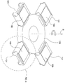
일 실시예에서, 도 1 내지 도 3에 도시한 바와 같은 회전 작동기 조립체(130)는 각각의 스크린 프린트 헤드(102) 내에서 수행된 스크린 인쇄 공정 중에 기판을 지지하도록 각각 구성되는 4 개의 프린팅 헤드(131)를 포함한다. 도 3은 기판이 4 개의 프린팅 헤드(131) 각각에 배열된 구성을 도시하는 회전 작동기 조립체(130)의 등각도이다. 회전 작동기 조립체(130)는 프린팅 네스트(131)가 시스템 내에 바람직하게 위치될 수 있도록 회전 작동기(도시 않음)와 시스템 제어기(101)의 사용에 의해 축선(B) 주위에서 회전되며 각도를 이루도록 위치될 수 있다. 회전 작동기 조립체(130)은 시스템(100) 내의 기판 처리 시퀀스를 수행하는데 사용되는 프린팅 네스트(131) 또는 다른 자동화 장치의 제어를 촉진시키는 하나 또는 그보다 많은 지원 구성요소들도 가질 수 있다.
In one embodiment, the
프린팅Printing 네스트의Nest 구성 Configuration
도 4에 도시한 바와 같이, 각각의 프린팅 네스트(131)는 일반적으로, 공급 스풀(135), 테이크-업 스풀(136), 및 공급 스풀(135)과 테이크-업 스풀(136)에 연결되고 지지대(138)에 위치되는 지지 재료(137)를 공급 및 유지하도록 구성되는 하나 또는 그보다 많은 작동기(도시 않음)를 가지는 컨베이어 조립체(139)로 구성된다. 상기 지지대(138)는 일반적으로 기판 지지면을 가지며, 그 지지면 위에 기판(150) 및 지지 재료(137)가 스크린 인쇄 공정이 스크린 프린트 헤드(102) 내에서 수행되는 동안에 위치된다. 일 실시예에서, 지지 재료(137)는 지지 재료(137)의 한쪽 면에 배열되는 기판(150)이 종래의 진공 발생 장치(예를 들어, 진공 펌프, 진공 분사기)에 의해 지지 재료(137)의 반대쪽 면에 가해지는 진공에 의해 지지대(138) 상에 유지될 수 있게 하는 다공성 재료이다. 일 실시예에서, 진공은 기판이 지지대의 기판 지지면(138A)에 척으로 고정될 수 있도록 지지대(138)의 기판 지지면(138A) 내에 형성된 진공 포트(도시 않음)에 가해진다. 일 실시예에서, 지지 재료(137)는 예를 들어, 담배용으로 사용되는 형태의 발산가능한(transpirable) 종이 또는 동일한 목적을 수행하는 다른 유사한 재료로 구성되는 발산가능한 재료이다.As shown in FIG. 4, each
일 구성에 있어서, 네스트 구동기구(148)는 지지 재료(137) 상에 위치되는 기판(150)의 운동이 프린팅 네스트(131) 내에서 정밀하게 제어될 수 있도록 공급 스풀(135) 및 테이크-업 스풀(136)에 연결되거나 그들과 결합하도록 구성된다. 일 실시예에서, 공급 스풀(135) 및 테이크-업 스풀(136)은 지지 재료(137)의 길이의 대향 단부들을 수용하도록 각각 구성된다. 일 실시예에서, 네스트 구동기구(148)는 지지대(138)를 가로지르는 지지 재료(137)의 운동 및 위치를 제어하기 위해 공급 스풀(135) 및/또는 테이크-업 스풀(136) 상에 위치되는 지지 재료(137)의 표면에 연결되거나 그 표면과 접촉되는 하나 또는 그보다 많은 구동 휠(147)을 포함한다. In one configuration, the nest drive mechanism 148 is adapted to supply the
도 4를 참조하면, 하나의 구성에서 지지대(138)를 가로지르는 지지 재료(137)의 장력과 운동은 공급 스풀(135) 및/또는 테이크-업 스풀(136)의 회전 운동을 제어할 수 있는 종래의 작동기(도시 않음)에 의해 제어된다. 일 구성에서, 지지 재료(137)는 공급 스풀(135)과 테이크-업 스풀(136) 사이의 어느 한 방향으로 이동하므로 복수의 풀리(140)에 의해 안내 및 지지된다.
Referring to FIG. 4, the tension and movement of the
건조 오븐의 구성Composition of drying oven
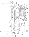
도 1은 일반적으로 기판(150)이 스크린 프린팅 헤드(102) 내에서 처리된 후에 유출 컨베이어(112)로부터 기판(150)을 수용하도록 각각 위치되는 두 개의 건조 챔버(200)를 포함하는 시스템 구성을 도시한다. 도 5 및 도 6은 일반적으로 이후에 더 상세히 설명되는 건조 챔버(200)의 하나 또는 그보다 많은 실시예들을 도시한다. 일반적으로, 건조 챔버(200)는 서멀 시스템(201)으로부터 서멀 시스템 내부에 위치되는 하나 또는 그보다 많은 기판으로 에너지가 분배되어 하나 또는 그보다 많은 기판의 표면 상에 증착된 재료들이 건조될 수 있는 처리 영역(202)을 포함한다. 일 예에서, 증착된 재료는 결정질 태양전지 기판 상에 배면 접점들을 형성하기 위한 태양전지 제조 공정에 공통적으로 사용되는 무연(lead free)알루미늄 시멘트 페이스트(예를 들어, Al 시멘트 6214)와 같은 알루미늄(Al) 함유 페이스트(paste)이다. 다른 예에서, 증착된 재료는 태양전지의 정면 쪽에 사용되는 은(Ag) 페이스트(예를 들어, 튜퐁에 의해 제조되는 PV 156(등록상표)) 또는 태양전지의 배면쪽에 사용되는 은-알루미늄(Ag/Al) 페이스트(튜퐁에 의해 제조되는 PV 202(등록상표))일 수 있다. 상기 처리 영역(202)은 다른 이송 장치(예를 들어, 유출 컨베이어(112))로부터 기판을 수용하고, 처리 영역(202) 내에 기판(150)을 이동 및/또는 위치시키도록 구성되는 건조 컨베이어(114)를 가진다.1 generally illustrates a system configuration that includes two drying
도 5는 건조 챔버(200) 내에 포함되는 서멀 시스템(201)의 일 실시예를 도시하는 측면 횡단면도이다. 서멀 시스템(201)은 일반적으로 복사 가열 조립체(204) 및 기판의 표면 상에 증착되는 재료를 급속 건조시키기 위해 함께 사용되는 대류 가열 조립체(203)를 포함한다. 이러한 구성에서, 대류 및 복사 열 전달 모드는 생산성을 개선하고 에너지 소모를 감소시키기 위해 건조 공정 중에 소정의 서멀 프로파일(예를 들어, 온도 대 시간)을 달성하도록 별도로 제어될 수 있다. 일 실시예에서, 건조 공정 중의 기판 온도는 약 150 ℃ 내지 약 300 ℃ 범위로 증가된다. 일반적으로, 기판 상에 형성된 패턴에 대한 손상을 방지하기 위해 증착된 재료 내의 결합제가 파괴되는 온도(예를 들어, 300 내지 350 ℃)를 초과하지 않는 것이 바람직하다.5 is a side cross-sectional view illustrating one embodiment of a
일 구성에 있어서, 도 5에 도시한 바와 같은 하나 또는 그보다 많은 기판(150)들이 건조기 컨베이어(114)를 사용하여 통로(D)를 따라 처리 영역(202)으로 이송된다. 건조기 컨베이어(114)는 일반적으로 처리 영역(202)을 통해 하나 또는 그보다 많은 기판을 이송 및/또는 위치시키는데 사용되는 자동화 기판 취급 장치이다. 일 실시예에서, 도 6에 도시한 바와 같이 건조기 컨베이어(114)는 처리 영역(202) 내에서의 처리 중에 기판(150)을 지지하도록 구성되는 단일 벨트(205)로 구성된다. 일 구성에서, 상기 벨트(205)는 처리 영역(202) 내에 도달되는 처리 온도에 견딜 수 있는 금속 벨트, 유리 섬유 함침(impregnated) 벨트, 세라믹 재료 함침 벨트, 또는 금속 함침 벨트이다. In one configuration, one or
상기 복사 가열 조립체(204)는 일반적으로 기판들이 처리 영역(202)을 통과할 때 벨트(205) 상에 놓인 기판에 에너지를 제공하는데 사용되는 하나 또는 그보다 많은 전자기 에너지 분배 장치를 포함한다. 일 실시예에서, 상기 전자기 에너지 분배 장치는 기판(150)에 하나 또는 그보다 많은 소정의 파장에서 복사 에너지를 분배하도록 구성 및/또는 선택되는 하나 또는 그보다 많은 램프(204A)(도 5 및 도 6)를 포함한다. 상기 복사 가열 조립체(204)로부터 분배되는 복사 에너지의 파장은 일반적으로 기판의 표면 상에 증착되는 재료에 의해 흡수되도록 선택된다. 그러나, 처리된 기판의 열 운영(budget)이 반도체 기판, 태양전지, 또는 다른 유사한 장치와 같은 대상물에 관한 것인 경우에, 복사 에너지가 일반적으로 기판을 형성한 재료에 의해 흡수되는 것이 아니고 증착된 재료에 의해 우선적으로 복사 에너지가 흡수되도록 기판으로 공급되는 복사 에너지의 파장을 제한하는 것이 바람직할 수 있다. 일 예에서, 기판이 실리콘 함유 재료로 제조되는 경우에 램프(204A)에 의해 분배되는 에너지의 파장은 일반적으로 약 1.06 ㎛인 실리콘의 흡수 에지보다 큰 파장만이 실리콘 기판에 의해 흡수되는 에너지 양을 감소시키기 위해 분배되도록 조절 또는 필터링될 수 있다.The
일 실시예에서, 복사 가열 조립체(204)에 의해 분배되는 최적 파장은 분배된 에너지의 흡수를 개선하기 위해 기판의 표면 상에 증착된 각각의 재료 형태 및 각각의 기판 형태 및 그에 따른 증착 재료의 건조 공정에 대해 선택 및/또는 조절된다. 일 실시예에서, 램프(204A)는 약 1200 ℃ 내지 1800 ℃ 범위의 최대 작동 온도를 가지며 약 1.4 ㎛보다 큰 파장에서 최대 방출능(power emission)을 가지는 적외선(IR) 램프이다. 일 예에서, 상기 램프(204A)는 독일 하나우 소재의 Heraeus Nobelight GmbH로부터 이용가능한 약 1 미터 길이의 이중 필라멘트 5 ㎾ 신속 중파 IR 램프이다. 몇몇 경우에 램프로 분배되는 전력을 조절하고 그에 따라 램프 내의 필라멘트의 온도를 조절함으로써[빈의 법칙(Wien's law)] 램프(204A)로부터 방출되는 복사선의 파장을 조절하는 것이 바람직하다. 그러므로, 시스템 제어기(101), 램프(204A)에 연결되는 파워 서플라이(도시 않음), 및 기판 표면 상에 증착된 재료의 광 흡수 특성에 대한 지식을 이용하는 것에 의해서, 램프(204A)에 의해 분배된 에너지의 파장은 건조 공정을 개선하도록 조절될 수 있다.In one embodiment, the optimum wavelength distributed by the
도 6은 처리 영역(202)의 소정 길이 내에 위치되고 그 소정 길이를 따라 연장하는 두 개의 램프(204A)를 이용하는 복사 가열 조립체(204)의 일 실시예를 도시한다. 이러한 구성에 있어서, 램프(204A)는 하나 또는 그보다 많은 기판들이 건조 공정 중에 램프(204A)의 길이를 따라 이송될 때 처리 영역(202) 내의 벨트(205) 상에 위치된 하나 또는 그보다 많은 기판으로 에너지를 이송하도록 위치된다(통로 "E"). 몇몇 경우에 서멀 시스템(201)의 다른 원하지 않는 부분들로 이송되는 열의 양을 감소시키고 에너지를 기판(150) 쪽으로 집중시키도록 램프(204A) 위에 하나 또는 그보다 많은 반사기(249)를 제공하는 것이 바람직할 수 있다. 또한, 몇몇 경우에 램프(204A)는 서멀 시스템(201)의 다른 원하지 않는 부분들로 이송되는 열의 양을 감소시키고 에너지를 기판(150) 쪽으로 집중시키도록 램프의 한 쪽에 배열되는 반사기를 가진다.6 illustrates one embodiment of a
서멀 시스템(201)은 또한 처리 영역(202) 내에 위치되는 기판의 표면 전체에 가열된 가스(예를 들어, 공기)를 분배하는 것과 같은 대류식 열 전달 방법을 사용하여 기판에 열을 전달하기 위한 대류 가열 조립체(203)도 사용한다. 대류식 열 전달 방법은 일반적으로 동일한 비율로 기판과 증착된 재료를 가열할 것이다. 기판 전도율이 실리콘 기판처럼 상당히 높은 경우에, 기판 전체에 걸친 온도 균일도는 상당히 균일하게 유지될 것이다. 대류식 열 전달률은 또한 대류 가스의 온도 및/또는 유동률을 조절함으로써 쉽게 제어될 수 있다.The
도 5를 참조하면, 대류 가열 조립체(203)는 일반적으로 유체 이송 장치(229), 플레넘(245) 및 가스 가열 조립체(240)를 포함한다. 따라서 처리 영역(202) 내에 분배된 기판은 유체 이송 장치(229)로부터 제공된 가스를 가열 조립체(240)를 통해 기판(150)의 표면을 통과하도록 지향시킴으로써 가열된다. 일 실시예에서, 유체 이송 장치(229)는 복사 가열 조립체(204)를 통해 처리 영역(202) 내측으로 소정 유동률의 가스를 분배할 수 있는(통로 "B" 참조) AC 팬이다.Referring to FIG. 5, the
상기 가스 가열 조립체(240)는 일반적으로 유체 이송 장치(229)로부터 분배되는 가스를 가열하도록 구성되는, 가열 영역(241) 내에 위치되는 하나 또는 그보다 많은 저항 가열 소자를 포함한다. 가스 가열 조립체(240)를 빠져나오는 가스의 온도는 종래의 가열 소자 온도 제어기(242), 하나 또는 그보다 많은 종래의 온도 감지 장치(도시 않음), 가열 영역(241) 내에 위치되는 저항 가열소자, 및 시스템 제어기(101)로부터 송신되는 명령어에 의해 제어될 수 있다. 일반적으로, 가열 영역(241) 내에 위치되는 저항 가열소자의 파워, 크기 및 길이는 분배 가스의 유동률 및 건조 공정 중에 도달하는 소정 가스의 온도에 의존할 것이다. 일 실시예에서, 가스 가열 조립체(240)의 출구에서의 가스 온도는 약 150 ℃ 내지 약 300 ℃ 범위로 제어된다.The
플레넘(245)은 일반적으로, 유체 이송 장치(229)로부터 분배되는 가스를 가스 가열 조립체(240)를 통해 플레넘 출구 섹션(243)으로 지향시킨 후에 처리 영역(202)을 통과하도록 지향시키는데 사용되는 둘러싸인 영역이다. 상기 플레넘(245)은 또한, 가스 복귀 또는 재순환 통로를 제공하여 공기와 같은 가열된 가스가 수집되고 재사용될 수 있도록 처리 영역(202)을 통해 이송되는 가스를 수용하도록 구성되는 플레넘 입구 섹션(244)을 포함할 수 있다. 따라서 재순환 통로는 일반적으로 열 교환 영역(246), 가열 조립체(240), 플레넘 출구 섹션(243), 처리 영역(202), 및 플레넘 입구 섹션(244)을 통과하는 통로(A1-A6)를 따른다. 가열된 가스의 재순환은 적어도 일부분이 처리 영역(202) 내측으로 재분배되기 이전에 소정 온도로 공기를 가열하는데 요구되는 에너지 양을 감소시키는데 커다란 도움이 될 수 있다.
일 실시예에서, 대류 가열 조립체(203)도 유체 이송 장치(229)에 의해 분배되는 가스 및 처리 영역(202)(참조 부호 A5-A6)으로부터 수용되는 재순환 가스로부터의 바람직하지 않은 오염을 제거하는데 사용되는 열 교환 장치(230)를 포함한다. 열 교환 장치(230)는 열 제어기(231)에 연결되는 하나 또는 그보다 많은 열 교환 표면(232) 및/또는 상기 플레넘(245)의 상기 섹션을 통과하는 가스로부터의 잠재적 오염물들을 제거하도록 구성되는 하나 또는 그보다 많은 필터형 구성요소들을 포함할 수 있다. 일반적으로, 열 제어기(231)는 재순환 가스 내에 포함된 어떤 휘발성 성분들을 응축 및 제거하기 위해 처리 영역(202)으로 분배되는 가열된 가스의 온도 미만의 온도로 열 교환 표면(232)의 온도를 유지하도록 구성된다. 상기 열 교환 표면(232)들도 유체 이송 장치(229)(즉, 통로 "B")로부터 가스 가열 조립체(240)로 분배되는 가스를 예열하는데 사용될 수 있다. 가스 가열 조립체(240)로 유입되기 이전에 가스를 예열하는 것도 가스 가열 효율을 개선함으로써 건조 챔버 내에서 수행되는 건조 공정의 전력 소모를 감소시키는데 도움을 줄 것이다. 에너지 소모가 태양전지 소자를 제조하기 위한 비용에서 종종 중요한 요소가 되므로, 본 발명에서 논의된 가스 예열 및/또는 재순환 방법들은 스크린 인쇄 제조 라인의 소유 비용 및 그에 따른 제조 소자의 제조 비용을 감소시키는데 도움을 줄 수 있다.In one embodiment, the
통상적으로, 재순환된 가스는 건조 공정 중에 증착된 재료로부터 배출되는 휘발 성분들의 휘발로 인해 재순환 가스 내에 수반된 하나 또는 그보다 많은 휘발 성분들의 양을 포함할 것이다. 휘발 성분들의 응축점 미만의 온도로 열 교환 표면(232)을 유지함으로써, 휘발 성분들은 응축될 것이며 재순환 가스로부터 제거된다. 열교환 장치(230) 내의 휘발 성분들을 포획하는 것은 또한, 재순환 가스에 의한 기판과 플레넘(245) 구성 요소들의 오염을 감소시키는데 도움을 줄 것이다. 일 예에서, 열 교환 표면(232)의 온도는 테르피놀(terpinol) 또는 에스테르와 같은 어떤 유기 용매를 제거하기 위해 <219 ℃의 온도로 유지된다. 일 실시예에서, 열 교환 표면(232)들은 재순환 가스 내에 수반된 증기 재료를 응축시키기 위해 약 40 ℃ 내지 약 80 ℃ 범위의 온도로 유지된다. 열 교환 표면(232)들의 온도는 종래의 재순환 유체형 또는 열전형 열 교환 장치와 같은 시스템 제어기(101) 및 열 제어기(231)의 사용에 의해 제어될 수 있다. 또한, 중력으로 인해 열 교환 표면(232) 상에 응축되는 휘발성 성분들은 플레넘(245)의 유체 수집 영역(233) 내로 유동하여 그 내부에 수집될 수 있다. 유체 수집 영역(233)은 폐기물 수집 시스템(도시 않음)으로 수집된 증기 재료를 분배하는데 사용되는 하나 또는 그보다 많은 배수구를 포함할 수 있다.Typically, the recycled gas will comprise the amount of one or more volatile components involved in the recycle gas due to the volatilization of volatile components released from the material deposited during the drying process. By maintaining the
또한, 상기 가스 내에 수반된 어떤 휘발 성분들을 수집하기 위해 열 교환 장치(230)를 사용하는 것도 두 번째로 처리 영역(202)을 통과하는 가스 부분 내의 증기의 부분 압력을 감소시키는데 도움을 줌으로써 증기의 상당한 잔류량이 재순환 가스 내에 유지되어 있는 경우에 허용될 수 있는 것보다, 증착된 재료로부터 배출되는 많은 양의 용매 재료를 상기 유동 가스가 수용할 수 있게 한다. 그러므로, 건조 공정을 완료하는데 요구되는 시간은 기판을 지나 유동하는 가스 내에 수용된 용매 재료의 양을 증가시킴으로써 감소될 수 있다.In addition, the use of
도 6은 도 5에 도시된 도면에 수직하고 상기 방향(A4)을 지향하는 처리 영역(202)에 대한 측면 횡단면도이다. 도 6에 도시된 바와 같이, 처리 영역(202)은 서멀 시스템(201)의 벽(251) 및 건조기 컨베이어(114)의 벽(114A)과 같은 하나 또는 그보다 많은 벽들에 의해 부분적으로 둘러싸여 있어서 대류 가열 조립체(203)에 의해 분배되는 가열 가스 및 복사 가열 조립체(204)에 의해 제공되는 열의 대부분이 손실되지 않는다. 도 5를 참조하면, 일 실시예에서 서멀 시스템(201) 및 처리 영역(202)은 하나 또는 그보다 많은 벽(207)에 의해 적어도 부분적으로 둘러싸인다. 일 구성에서, 상기 벽(207)은 처리 영역(202)의 대향 단부들에 작은 개구(208)를 가짐으로써, 기판이 벨트(205)의 사용에 의해 처리 영역(202) 내외로 이송될 수 있는 반면에, 건조 챔버(200)를 빠져나가는 가열 가스의 양은 최소화한다. 처리 영역(202)을 부분적으로 에워싸는 것도 처리 영역(202)을 통해 유동하는 가스 내에서 발견되는 어떤 오염물들이 인접한 어떤 처리 챔버들을 오염시키는 것을 방지하는데 도움을 줄 수 있다.FIG. 6 is a side cross-sectional view of the
일 실시예에서, 내측 차폐물(252)은 플레넘 출구 섹션(243)의 출구 포트(243A)로부터 제공되는 유동 가스를 처리 영역(202) 내에 위치되는 기판(150)을 가로지르도록 그리고 플레넘 입구 섹션(244)의 입구 포트(244A)로 추가로 지향시키는데 사용된다. 내측 차폐물(252)은 또한 복사 가열 조립체(204)에 의해 제공된 어떤 열을 벨트(205) 상에 위치된 기판(150)으로 반사시키고 추가로 지향시키는데 사용될 수도 있다.In one embodiment, the
대류 가열 조립체(203) 및 복사 가열 조립체(204)에 의해 제공된 열을 조절함으로써 상기 건조 공정은 증착된 재료의 건조 시간을 개선하고 건조 공정에서 유발될 수 있는 어떤 잠재적인 열 운영 문제점들을 감소시키도록 조절 및/또는 최적화될 수 있다. 일 실시예에서, 도 5에 도시한 바와 같이 대류 가스 유동은 온도 램프 업 속도(temperature ramp up rate)를 개선하고 유입 기판을 예열하기 위해 처리 영역(202)을 통과하는 기판(150)의 운동 방향(즉, "D" 방향)과 반대인 방향(즉, "A4" 방향)으로 분배된다. 또한, 실리콘 기판이 IR 파장 내의 낮은 흡수 계수를 가지므로, 열 전달 효율 및 그에 따른 기판 건조에 요구되는 시간은 대류 열 전달 및 복사 열 전달 모드들의 조합에 의해 현저히 감소될 수 있다. 증가된 열 전달 효율로 인해 건조된 각각의 기판에 대한 서멀 프로파일이 개선되는데, 이는 처리 온도가 높을수록 더욱 쉽게 달성되기 때문이다.By regulating the heat provided by the
본 발명에서 설명된 방법의 사용으로 증착된 재료가 건조될 수 있게 하기 위해 종래의 스크린 인쇄 공정에 통상적으로 사용되는 버퍼링 장치에 대한 필요성도 감소시킬 수 있는데, 이는 종래의 단지 복사 건조 공정에서의 사이클 시간이 종종 너무 비효율적이고 너무 길어서 나머지 제조 라인의 생산성을 저하시키기 때문이라고 생각된다. 대류 열 전달 및 파장 제어된 복사 가열의 사용으로 각각의 건조 챔버(200) 내의 기판 가열 사이클은 건조 오븐 생산량이 약 2 미터의 길이보다 짧은 시스템 내에서 시간 당 1400 개의 결정질 실리콘 156 mm × 156 mm 기판을 초과할 수 있도록 감소될 것이라고 생각된다. 따라서 본 발명에서 설명된 급열 처리 방법은 사이클 시간을 감소시키며, 건조 챔버(200)가 차지하는 플로어 공간을 감소시키며, 또한 기판을 건조시키는데 필요한 소유비용을 감소시킬 것으로 생각된다.The use of the method described herein can also reduce the need for a buffering device commonly used in conventional screen printing processes to allow the deposited material to dry, which is a cycle in conventional only radiation drying processes. It is believed that the time is often too inefficient and too long to reduce the productivity of the remaining manufacturing lines. Substrate heating cycles in each drying
도 7은 처리 영역(202)(즉, 통로 A5 및 A6)으로부터 복귀하는 가스가 재순화되지 않는 도 5 및 도 6에 도시된 서멀 시스템(201)의 다른 실시예에 대한 측면 횡단면도이다. 이러한 구성에서, 유체 이송 장치(229)(예를 들어, 통로 "B")를 빠져나오는 가스는 복수의 열 교환 튜브(248)를 통과해 입구 플레넘(249A)으로 유입되며 가스 가열 조립체(240) 및 처리 영역(202)을 통해 분배되기 이전에 출구 플레넘(249B)으로 유입된다. 열 교환 튜브(248)는 통로 "B"를 따르는 가스가 튜브의 내측 영역(248A)을 통과하여 처리 영역(202)으로부터 복귀하는 가스와 혼합되지 않도록 일반적으로 밀봉된다. 일 구성에서, 통로(A5 및 A6)를 따라 처리 영역(202)으로부터 복귀하는 가스는 포트(247)를 통해 서멀 시스템(201)으로부터 배출되기 이전에 열 교환 튜브(248)의 외측 표면을 통과한다. 그러므로, 열 제어기(231)를 사용하여 열 교환 튜브(248)의 온도를 제어함으로써, 유체 이송 장치(229)로부터 가스 가열 조립체(240)로 유동하는 가스의 온도가 예열될 수 있으며, 처리 영역(202)으로부터 복귀하는 가스가 수반된 어떤 휘발 성분들을 제거하도록 냉각될 수 있다. 일반적으로, 열 제어기(231)는 통로(A6)를 따라 유동하는 가스 내에 포함된 어떤 휘발 성분을 응축 및 제거하기 위해 처리 영역(202)으로 분배되는 가열된 가스의 온도 미만의 온도로 열 교환 튜브(248)의 표면(즉, 열 교환 표면(232))의 온도를 유지하도록 구성된다. 중력으로 인해 열 교환 튜브(248) 상에 응축되는 휘발 성분들은 플레넘(245)의 유체 수집 영역(223)으로 유동되(즉, 통로 "C")고 그 내부에 수집될 것이다. 유체 수집 영역(233)은 폐기물 수집 시스템(도시 않음)으로 수집된 증기 재료를 분배하는데 사용되는 하나 또는 그보다 많은 배수구를 포함할 수 있다.FIG. 7 is a side cross-sectional view of another embodiment of the
전술한 설명은 본 발명의 실시예들에 관한 것이지만, 본 발명의 다른 추가의 실시예들이 본 발명의 기본 범주로부터 이탈함이 없이 창안될 수 있으며 본 발명의 범주는 다음의 특허청구범위에 의해 결정된다.
While the foregoing description is directed to embodiments of the invention, other additional embodiments of the invention may be devised without departing from the basic scope thereof, and the scope thereof is determined by the claims that follow. do.
Claims (15)
처리 영역을 통해 하나 또는 그보다 많은 기판을 이송하도록 구성되는 제 1 컨베이어와,
상기 제 1 컨베이어 상에 위치된 하나 또는 그보다 많은 기판으로 하나 또는 그보다 많은 파장에서 전자기 에너지를 분배하도록 구성되는 복사 열 전달 조립체, 및
내부에 배열되는 가열 소자를 갖는 플레넘, 및 상기 플레넘 내에 배열되는 상기 가열 소자를 지나치게 그리고 상기 처리 영역 내의 상기 제 1 컨베이어 상에 위치된 기판의 표면을 지나치게 가스를 이동시키도록 구성되는 유체 분배 장치를 포함하는 대류 열 전달 조립체를 포함하는,
기판 처리 장치.
As a substrate processing apparatus,
A first conveyor configured to transport one or more substrates through the processing region,
A radiant heat transfer assembly configured to distribute electromagnetic energy at one or more wavelengths to one or more substrates located on the first conveyor, and
A plenum having a heating element arranged therein, and a fluid distribution configured to move gas excessively over the heating element arranged within the plenum and over the surface of the substrate located on the first conveyor in the processing region A convection heat transfer assembly comprising a device,
Substrate processing apparatus.
상기 대류 열 전달 조립체는,
상기 기판 표면을 지나치게 이동된 상기 가스를 수용하도록 위치되는 입구 포트를 갖는 상기 플레넘, 및
상기 입구 포트를 통해 수용된 가스와 유체 소통되는 열 교환 표면을 갖는 열 교환 조립체를 더 포함하는,
기판 처리 장치.
The method of claim 1,
The convection heat transfer assembly,
The plenum having an inlet port positioned to receive the gas excessively moved over the substrate surface, and
Further comprising a heat exchange assembly having a heat exchange surface in fluid communication with the gas received through the inlet port,
Substrate processing apparatus.
상기 열 교환 조립체는 상기 열 교환 표면과 열 소통되며 상기 입구 포트를 통해 수용된 가스로부터 열을 제거하도록 구성되는 열 제어기를 더 포함하는,
기판 처리 장치.
The method of claim 2,
The heat exchange assembly further comprises a heat controller in thermal communication with the heat exchange surface and configured to remove heat from the gas received through the inlet port,
Substrate processing apparatus.
상기 제 1 컨베이어 및 상기 처리 영역을 부분적으로 에워싸는 하나 또는 그보다 많은 벽을 더 포함하며,
상기 플레넘은 상기 가열 소자와 상기 처리 영역 사이에 위치되는 출구 포트를 더 포함하며, 상기 유체 분배 장치에 의해 분배되는 가스는 상기 입구 포트로 유입되기 이전에 상기 처리 영역을 부분적으로 에워싸는 하나 또는 그보다 많은 벽들 사이로 상기 출구 포트를 통해 유동하도록 구성되는,
기판 처리 장치.
The method of claim 2,
Further comprising one or more walls partially enclosing said first conveyor and said processing region,
The plenum further comprises an outlet port located between the heating element and the treatment region, wherein gas dispensed by the fluid dispensing device partially surrounds the treatment region prior to entering the inlet port. Configured to flow through the outlet port between walls,
Substrate processing apparatus.
하나 또는 그보다 많은 램프 및 상기 램프에 전기 접속되는 파워 서플라이를 갖는 상기 복사 열 전달 조립체, 및
상기 기판으로 상기 램프에 의해 분배되는 전자기 에너지의 파장을 조절하도록 구성되는 제어기를 더 포함하는,
기판 처리 장치.
The method of claim 1,
The radiant heat transfer assembly having one or more lamps and a power supply electrically connected to the lamps, and
And a controller configured to adjust a wavelength of electromagnetic energy distributed by the lamp to the substrate.
Substrate processing apparatus.
상기 컨베이어는 상기 처리 장치를 통해 그리고 상기 입구 포트와 출구 포트를 지나치게 기판을 이송하도록 구성되는 벨트를 포함하는,
기판 처리 장치.
The method of claim 4, wherein
The conveyor comprises a belt configured to convey the substrate excessively through the processing apparatus and through the inlet and outlet ports,
Substrate processing apparatus.
회전 작동기에 연결되는 제 1 기판 지지대와,
상기 회전 작동기가 제 1 방위에 각위치될 때 상기 제 1 기판 지지대를 수용하도록 위치되는 제 1 스크린 인쇄 챔버, 및
상기 회전 작동기가 제 2 방위에 각위치될 때 상기 제 1 기판 지지대로부터 기판을 이송하도록 위치되며, 상기 제 1 컨베이어와 이송가능하게 소통되는 제 2 컨베이어를 더 포함하는,
기판 처리 장치.
The method of claim 1,
A first substrate support connected to the rotary actuator,
A first screen printing chamber positioned to receive the first substrate support when the rotary actuator is angularly positioned in a first orientation, and
And further comprising a second conveyor positioned to transport the substrate from the first substrate support when the rotary actuator is angularly positioned in a second orientation, the second conveyor being in transferable communication with the first conveyor.
Substrate processing apparatus.
상기 회전 작동기에 연결되는 제 2 기판 지지대와,
상기 회전 작동기가 상기 제 1 방위에 각위치될 때 상기 제 2 기판 지지대로 기판을 이송하도록 위치되는 제 3 컨베이어, 및
상기 회전 작동기가 상기 제 1 방위에 각위치될 때 상기 제 2 기판 지지대로부터 기판을 수용하도록 위치되는 제 4 컨베이어를 더 포함하는,
기판 처리 장치.
The method of claim 7, wherein
A second substrate support coupled to the rotary actuator;
A third conveyor positioned to transfer a substrate to the second substrate support when the rotary actuator is angularly positioned in the first orientation, and
Further comprising a fourth conveyor positioned to receive the substrate from the second substrate support when the rotary actuator is angularly positioned in the first orientation,
Substrate processing apparatus.
상기 대류 열 전달 조립체는,
상기 플레넘 내에 배열되는 복수의 열 교환 튜브로서, 상기 유체 분배 장치가 상기 복수의 열 전달 튜브의 제 1 표면, 상기 가열 소자, 및 상기 처리 영역 내에 위치된 하나 또는 그보다 많은 기판 각각의 표면 전체에 걸쳐 가스를 이동시키도록 구성되는, 복수의 열 교환 튜브와,
상기 복수의 열 교환 튜브의 온도를 제어하도록 구성되는 열 교환 장치, 및
하나 또는 그보다 많은 기판의 표면을 지나치게 이동된 상기 가스를 수용하며 상기 복수의 열 교환 튜브의 제 2 표면을 지나치게 수용된 상기 가스를 지향시키도록 위치되는 플레넘 입구를 더 포함하는,
기판 처리 장치.
The method of claim 1,
The convection heat transfer assembly,
A plurality of heat exchange tubes arranged in the plenum, the fluid dispensing device being provided throughout the first surface of the plurality of heat transfer tubes, the heating element, and the surface of each of one or more substrates located within the processing region. A plurality of heat exchange tubes, configured to move the gas over,
A heat exchange device configured to control a temperature of the plurality of heat exchange tubes, and
Further comprising a plenum inlet positioned to receive the gas that has been excessively moved over the surface of one or more substrates and to direct the gas that is excessively received to the second surface of the plurality of heat exchange tubes,
Substrate processing apparatus.
스크린 인쇄 챔버 내에 기판을 위치시킨 후에 스크린 인쇄 공정을 사용하여 상기 기판 상에 재료를 증착하는 단계와,
상기 재료의 증착 이후에 건조 챔버의 처리 영역으로 상기 기판을 이송하는 단계와,
상기 처리 영역 내에 위치된 상기 기판의 표면으로 일정량의 전자기 에너지를 분배하는 단계, 및
상기 처리 영역 내에 위치된 상기 기판의 표면을 지나치게 가열된 가스를 분배하는 단계를 포함하는,
기판 처리 방법.
As a substrate processing method,
Depositing material on the substrate using a screen printing process after positioning the substrate in the screen printing chamber;
Transferring the substrate to a processing region of a drying chamber after deposition of the material;
Distributing an amount of electromagnetic energy to a surface of the substrate located within the processing region, and
Distributing an overheated gas over the surface of the substrate located within the processing region,
Substrate processing method.
일정량의 전자기 에너지를 분배하는 단계는,
상기 기판 내에 포함된 하나 또는 그보다 많은 재료에 의해 흡수된 에너지의 양을 최소화하면서, 상기 증착된 재료에 의한 전자기 에너지의 흡수를 촉진시키도록 하나 또는 그보다 많은 소정의 파장에서 상기 전자기 에너지를 제공하는 단계를 더 포함하는,
기판 처리 방법.
The method of claim 10,
Distributing a certain amount of electromagnetic energy,
Providing the electromagnetic energy at one or more predetermined wavelengths to facilitate absorption of electromagnetic energy by the deposited material while minimizing the amount of energy absorbed by one or more materials contained within the substrate. Further comprising,
Substrate processing method.
가열된 가스를 분배하는 단계는,
열 교환 표면의 온도를 제어하는 단계, 및
상기 가열된 가스가 상기 기판을 지나치게 분배된 이후에 상기 가열된 가스의 적어도 일부분을 상기 열 교환 표면으로 분배하는 단계를 더 포함하며,
상기 열 교환 표면의 온도는 상기 가열된 가스의 일부분 내에 포함된 휘발 성분이 상기 열 교환 표면 상에 응축되도록 제어되는,
기판 처리 방법.
The method of claim 10,
Distributing the heated gas,
Controlling the temperature of the heat exchange surface, and
Distributing at least a portion of the heated gas to the heat exchange surface after the heated gas has been excessively dispensed with the substrate,
The temperature of the heat exchange surface is controlled such that volatile components contained within the portion of the heated gas condense on the heat exchange surface,
Substrate processing method.
상기 열 교환 표면의 온도는 약 40 ℃ 내지 약 300 ℃ 범위인,
기판 처리 방법.
The method of claim 12,
The temperature of the heat exchange surface is in a range from about 40 ° C. to about 300 ° C.,
Substrate processing method.
가열된 가스를 분배하는 단계는,
가열 소자를 지나치게 상기 가스를 유동시킴으로써 가스를 가열하는 단계와,
상기 처리 영역의 범위를 통해 상기 가열된 가스를 지향시키는 단계, 및
상기 처리 영역을 통해 지향된 상기 가열된 가스의 적어도 일부분을 수용하며, 상기 가열된 가스의 일부분을 재순환시키도록 상기 가열 소자를 지나치게 적어도 상기 가열된 가스의 일부분을 분배하는 단계를 더 포함하는,
기판 처리 방법.
The method of claim 10,
Distributing the heated gas,
Heating the gas by flowing the gas excessively through a heating element;
Directing the heated gas through the range of the processing region, and
Receiving at least a portion of the heated gas directed through the processing region, and dispensing the portion of the heated gas excessively at least a portion of the heating element to recycle a portion of the heated gas;
Substrate processing method.
상기 기판은 실리콘 함유 기판인,
기판 처리 방법.
The method of claim 10,
The substrate is a silicon-containing substrate,
Substrate processing method.
Applications Claiming Priority (8)
| Application Number | Priority Date | Filing Date | Title |
|---|---|---|---|
| ITUD2008A000135 | 2008-06-11 | ||
| ITUD20080135 ITUD20080135A1 (en) | 2008-06-11 | 2008-06-11 | LOW THERMAL PROFILE OVEN FOR SCREEN PRINTING |
| ITUD2008A000154 | 2008-06-27 | ||
| ITUD20080154 ITUD20080154A1 (en) | 2008-06-27 | 2008-06-27 | LOW THERMAL PROFILE OVEN FOR SCREEN PRINTING |
| US12/240,955 | 2008-09-29 | ||
| US12/240,955 US20090308860A1 (en) | 2008-06-11 | 2008-09-29 | Short thermal profile oven useful for screen printing |
| US12/273,442 | 2008-11-18 | ||
| US12/273,442 US20090311439A1 (en) | 2008-06-11 | 2008-11-18 | Short Thermal Profile Oven Useful For Screen Printing |
Publications (1)
| Publication Number | Publication Date |
|---|---|
| KR20110030564A true KR20110030564A (en) | 2011-03-23 |
Family
ID=41151966
Family Applications (1)
| Application Number | Title | Priority Date | Filing Date |
|---|---|---|---|
| KR1020117000750A KR20110030564A (en) | 2008-06-11 | 2009-05-29 | Short thermal profile oven useful for screen printing |
Country Status (7)
| Country | Link |
|---|---|
| US (2) | US20090308860A1 (en) |
| EP (1) | EP2301064B1 (en) |
| JP (1) | JP2011526734A (en) |
| KR (1) | KR20110030564A (en) |
| CN (2) | CN102057462B (en) |
| TW (1) | TWI479590B (en) |
| WO (1) | WO2009150070A1 (en) |
Cited By (7)
| Publication number | Priority date | Publication date | Assignee | Title |
|---|---|---|---|---|
| KR20150074190A (en) * | 2012-11-30 | 2015-07-01 | 카티바, 인크. | Gas enclosure assembly and system |
| US10442226B2 (en) | 2008-06-13 | 2019-10-15 | Kateeva, Inc. | Gas enclosure assembly and system |
| US11034176B2 (en) | 2008-06-13 | 2021-06-15 | Kateeva, Inc. | Gas enclosure assembly and system |
| US11107712B2 (en) | 2013-12-26 | 2021-08-31 | Kateeva, Inc. | Techniques for thermal treatment of electronic devices |
| US11338319B2 (en) | 2014-04-30 | 2022-05-24 | Kateeva, Inc. | Gas cushion apparatus and techniques for substrate coating |
| US11489119B2 (en) | 2014-01-21 | 2022-11-01 | Kateeva, Inc. | Apparatus and techniques for electronic device encapsulation |
| US11633968B2 (en) | 2008-06-13 | 2023-04-25 | Kateeva, Inc. | Low-particle gas enclosure systems and methods |
Families Citing this family (20)
| Publication number | Priority date | Publication date | Assignee | Title |
|---|---|---|---|---|
| CN101321604B (en) * | 2005-12-06 | 2011-09-14 | 武藏高科技有限公司 | Processing apparatus and method |
| WO2011110231A1 (en) * | 2010-03-12 | 2011-09-15 | Q-Cells Se | Method and in-line production system for the production of solar cells |
| US20120060758A1 (en) * | 2011-03-24 | 2012-03-15 | Primestar Solar, Inc. | Dynamic system for variable heating or cooling of linearly conveyed substrates |
| US9589817B2 (en) * | 2011-04-15 | 2017-03-07 | Illinois Tool Works Inc. | Dryer |
| US10676847B2 (en) | 2014-11-07 | 2020-06-09 | Illinois Tool Works Inc. | Discharge nozzle plate for center-to-ends fiber oxidation oven |
| US10458710B2 (en) | 2014-11-07 | 2019-10-29 | Illinois Tool Works Inc. | Supply plenum for center-to-ends fiber oxidation oven |
| CN104441956B (en) * | 2014-12-10 | 2017-05-24 | 苏州互强工业设备有限公司 | Silk-printing drying line |
| CN104527218B (en) * | 2014-12-24 | 2016-01-13 | 庄统壹 | A kind of screen printer and the process utilizing this screen printer to print |
| KR20180099844A (en) * | 2016-02-22 | 2018-09-05 | 어플라이드 머티어리얼스 이탈리아 에스.알.엘. | Apparatus for processing solar cell substrates, systems for processing solar cell substrates, and methods for processing solar cell substrates |
| GB2562503A (en) * | 2017-05-16 | 2018-11-21 | Asm Assembly Systems Singapore Pte Ltd | Workpiece transfer and printing |
| WO2019081041A1 (en) * | 2017-10-27 | 2019-05-02 | Applied Materials Italia S.R.L. | Apparatus configured to determine a state of a deposition arrangement, system for the manufacture of a solar cell, and method for determining a state of a deposition arrangement |
| CN110534611A (en) * | 2018-05-25 | 2019-12-03 | 米亚索乐装备集成(福建)有限公司 | A kind of heating equipment for small disc type batteries |
| DE102018210558A1 (en) * | 2018-06-28 | 2019-02-28 | Heidelberger Druckmaschinen Ag | Printing device with a planar motor system |
| KR102088778B1 (en) * | 2018-08-07 | 2020-03-13 | 김영택 | Thermal drying equipment of printing machine using water-soluble ink |
| EP3725525B1 (en) * | 2019-04-18 | 2024-02-28 | Exentis Knowledge GmbH | Device and method for the preparation of three-dimensional screen printing workpieces |
| EP3725526A1 (en) * | 2019-04-18 | 2020-10-21 | Exentis Knowledge GmbH | Method for producing three-dimensional screen printing workpieces |
| EP4319508A3 (en) * | 2019-04-18 | 2024-03-27 | Exentis Knowledge GmbH | Device and method for producing three-dimensional screen printing workpieces |
| CN111186211B (en) * | 2020-02-04 | 2021-06-04 | 北部湾大学 | Printing ink drying device for ceramic decal paper printing machine |
| CN114801452A (en) * | 2021-01-18 | 2022-07-29 | 博泽精密科技(苏州)有限公司 | Automatic feeding mechanism of printing machine |
| CN215305176U (en) * | 2021-06-15 | 2021-12-28 | 江门市新会恒隆家居创新用品有限公司 | Toaster |
Family Cites Families (57)
| Publication number | Priority date | Publication date | Assignee | Title |
|---|---|---|---|---|
| US3216127A (en) * | 1962-02-09 | 1965-11-09 | Universal Oil Prod Co | Coating oven with catalytic incineration of volatiles |
| US3961569A (en) * | 1974-08-15 | 1976-06-08 | The United States Of America As Represented By The Secretary Of The Army | Apparatus for continuous microwave sterilization of food in pouches |
| US3924569A (en) * | 1974-08-28 | 1975-12-09 | Goodyear Tire & Rubber | Apparatus for treating tire cord fabric |
| SE455479B (en) * | 1982-03-17 | 1988-07-18 | Svecia Silkscreen Maskiner Ab | DRYING FOR A PRINT ON A MATERIAL |
| US4565917B1 (en) * | 1984-01-18 | 1999-06-08 | Vitronics Corp | Multi-zone thermal process system utilizing nonfocused infared panel emitters |
| US4753735A (en) * | 1985-03-11 | 1988-06-28 | Allied-Signal Inc. | Solvent and apparatus and method for cleaning and drying surfaces of non absorbent articles |
| US4694586A (en) * | 1985-05-17 | 1987-09-22 | David Reznik | Apparatus and method for drying and curing coated substrates |
| CH671231A5 (en) * | 1985-07-24 | 1989-08-15 | Basf Ag | |
| US4757759A (en) * | 1986-03-05 | 1988-07-19 | Tam Ceramics, Inc. | Multilayer ceramic bar printing and assembling apparatus |
| DE3633106A1 (en) * | 1986-09-30 | 1988-03-31 | Pagendarm Beschichtungstechnik | METHOD AND DEVICE FOR COATING A MOVING SUPPORT MATERIAL WITH A COATING AGENT CONTAINING A SOLVENT |
| US4798007A (en) * | 1987-05-28 | 1989-01-17 | Eichenlaub John E | Explosion-proof, pollution-free infrared dryer |
| DE8817120U1 (en) * | 1988-04-07 | 1993-02-04 | Vits Maschinenbau Gmbh, 4018 Langenfeld, De | |
| JPH01262069A (en) * | 1988-04-13 | 1989-10-18 | Matsushita Electric Ind Co Ltd | Heating device for substrate and heating method |
| US5883362A (en) * | 1988-05-19 | 1999-03-16 | Quadlux, Inc. | Apparatus and method for regulating cooking time in a lightwave oven |
| JPH0248132Y2 (en) * | 1988-09-16 | 1990-12-18 | ||
| US5263265A (en) * | 1989-10-23 | 1993-11-23 | Despatch Industries | Convection/radiation material treatment oven |
| DE69107170T2 (en) * | 1990-11-16 | 1995-06-08 | Setsuo Tate | Drying methods and devices for a coated substrate. |
| IT1252949B (en) * | 1991-09-30 | 1995-07-06 | Gisulfo Baccini | PROCEDURE FOR THE PROCESSING OF GREEN-TAPE TYPE CIRCUITS AND DEVICE ADOPTING THIS PROCEDURE |
| JPH0694369A (en) * | 1992-09-14 | 1994-04-05 | Tdk Corp | Atmospheric gas controller for firing furnace |
| US5467912A (en) * | 1992-11-27 | 1995-11-21 | Hitachi Techno Engineering Co., Ltd. | Reflow soldering apparatus for soldering electronic parts to circuit substrate |
| JP3226651B2 (en) * | 1993-02-02 | 2001-11-05 | 千住金属工業株式会社 | Reflow furnace and cooling device for reflow furnace |
| JPH0899610A (en) * | 1994-09-30 | 1996-04-16 | Tsutsunaka Plast Ind Co Ltd | Synthetic-resin-made window material having anti-fog performance and manufacture thereof |
| JP2718007B2 (en) * | 1995-06-06 | 1998-02-25 | 太陽インキ製造株式会社 | Alkali-developable one-pack type photo solder resist composition and method for manufacturing printed wiring board using the same |
| AU2139197A (en) * | 1996-03-29 | 1997-10-22 | Minnesota Mining And Manufacturing Company | Apparatus and method for drying a coating on a substrate employing multiple drying subzones |
| TW466772B (en) * | 1997-12-26 | 2001-12-01 | Seiko Epson Corp | Method for producing silicon oxide film, method for making semiconductor device, semiconductor device, display, and infrared irradiating device |
| JP3754841B2 (en) * | 1998-06-11 | 2006-03-15 | キヤノン株式会社 | Photovoltaic element and manufacturing method thereof |
| CA2271401C (en) * | 1999-02-23 | 2008-07-29 | Tesco Corporation | Drilling with casing |
| JP2000238233A (en) * | 1999-02-23 | 2000-09-05 | Fuji Mach Mfg Co Ltd | Method and equipment for inspecting screen, and screen printer |
| JP3934281B2 (en) * | 1999-07-02 | 2007-06-20 | 三菱電機株式会社 | Conveyor furnace |
| KR100671986B1 (en) * | 1999-07-12 | 2007-01-23 | 타이요 잉크 메뉴펙츄어링 컴퍼니, 리미티드 | Alkalidevelopment type photocurable composition and pattern of burned matter obtained from the same |
| CN1211807C (en) * | 2000-02-21 | 2005-07-20 | 东洋油墨制造株式会社 | Active energy beam curing type conductive paste, production method and device for conductor circuit substrate and non-contact ID and production method thereof |
| CN1237085C (en) * | 2000-09-20 | 2006-01-18 | 太阳油墨制造株式会社 | Carboxylated photosensitive resin, alkali-developable photocurable/heat-curable composition containing the same, and cured article obtained therefrom |
| JP2002225221A (en) * | 2001-02-02 | 2002-08-14 | Matsushita Electric Ind Co Ltd | Screen press and method for screen printing |
| JP3910054B2 (en) * | 2001-12-10 | 2007-04-25 | 東京エレクトロン株式会社 | Substrate processing equipment |
| JP2004140120A (en) * | 2002-10-16 | 2004-05-13 | Canon Inc | Polycrystalline silicon substrate |
| JP2004181483A (en) * | 2002-12-03 | 2004-07-02 | Senju Metal Ind Co Ltd | Reflow furnace |
| JP4042592B2 (en) * | 2003-03-05 | 2008-02-06 | ウシオ電機株式会社 | Heating device |
| EP2610567A1 (en) * | 2003-03-26 | 2013-07-03 | Fujifilm Corporation | Drying method for a coating layer |
| US20040226513A1 (en) * | 2003-05-12 | 2004-11-18 | Applied Materials, Inc. | Chamber for uniform heating of large area substrates |
| US7485410B2 (en) * | 2004-06-30 | 2009-02-03 | Canon Kabushiki Kaisha | Method of manufacturing thick dielectric pattern and method of manufacturing image displaying apparatus |
| KR101071004B1 (en) * | 2004-12-22 | 2011-10-06 | 가부시키가이샤 소쿠도 | Integrated thermal unit |
| US20060130767A1 (en) * | 2004-12-22 | 2006-06-22 | Applied Materials, Inc. | Purged vacuum chuck with proximity pins |
| FR2886577B1 (en) * | 2005-06-06 | 2008-12-26 | Mach Dubuit Soc Par Actions Si | MACHINE AND PRINTING DEVICE BY SCREEN PRINTING |
| JP4319647B2 (en) * | 2005-06-30 | 2009-08-26 | 株式会社タムラ古河マシナリー | Reflow furnace |
| JP4622705B2 (en) * | 2005-07-01 | 2011-02-02 | パナソニック株式会社 | Movable contact for panel switch |
| WO2007136598A2 (en) * | 2006-05-19 | 2007-11-29 | Nu-Vu Food Service Systems | Combination conveyor oven |
| US7805064B2 (en) * | 2006-06-26 | 2010-09-28 | TP Solar, Inc. (Corporation of CA, USA) | Rapid thermal firing IR conveyor furnace having high intensity heating section |
| KR100856411B1 (en) * | 2006-12-01 | 2008-09-04 | 삼성전자주식회사 | Method and apparatus for compensating illumination compensation and method and apparatus for encoding moving picture based on illumination compensation, and method and apparatus for encoding moving picture based on illumination compensation |
| US7851727B2 (en) * | 2007-05-16 | 2010-12-14 | Prince Castle LLC | Method of controlling an oven with hybrid heating sources |
| ITUD20080136A1 (en) * | 2008-06-13 | 2009-12-14 | Baccini S P A | PLANT FOR PROCESSING PLATES FOR ELECTRONIC CIRCUITS |
| IT1392993B1 (en) * | 2009-02-23 | 2012-04-02 | Applied Materials Inc | SUPPORT MATERIAL SUBSTRATE IMPROVED USEFUL FOR PRINTING PRINTING PROCEDURES |
| IT1392992B1 (en) * | 2009-02-23 | 2012-04-02 | Applied Materials Inc | PROCEDURE AND EQUIPMENT FOR THE SERIGRAPHIC PRINTING OF A MULTIPLE LAYER DIAGRAM |
| IT1392991B1 (en) * | 2009-02-23 | 2012-04-02 | Applied Materials Inc | AUTOREGULATING SERIGRAPHIC PRINTING PROCEDURE |
| US8828776B2 (en) * | 2009-04-16 | 2014-09-09 | Tp Solar, Inc. | Diffusion furnaces employing ultra low mass transport systems and methods of wafer rapid diffusion processing |
| WO2010121190A1 (en) * | 2009-04-16 | 2010-10-21 | Tp Solar, Inc. A Corporation Of Ca | Diffusion furnaces employing ultra low mass transport systems and methods of wafer rapid diffusion processing |
| IT1394811B1 (en) * | 2009-07-08 | 2012-07-13 | Applied Materials Inc | APPARATUS AND PROCEDURE FOR THE MANIPULATION OF DAMAGED SUBSTRATES IN SUBSTRATE PROCESSING SYSTEMS |
| IT1398433B1 (en) * | 2009-09-03 | 2013-02-22 | Applied Materials Inc | APPARATUS AND PROCEDURE FOR PROCESSING A SUBSTRATE |
-
2008
- 2008-09-29 US US12/240,955 patent/US20090308860A1/en not_active Abandoned
- 2008-11-18 US US12/273,442 patent/US20090311439A1/en not_active Abandoned
-
2009
- 2009-05-29 EP EP09761633.8A patent/EP2301064B1/en not_active Not-in-force
- 2009-05-29 KR KR1020117000750A patent/KR20110030564A/en active IP Right Grant
- 2009-05-29 WO PCT/EP2009/056663 patent/WO2009150070A1/en active Application Filing
- 2009-05-29 JP JP2011512930A patent/JP2011526734A/en active Pending
- 2009-05-29 CN CN2009801225813A patent/CN102057462B/en not_active Expired - Fee Related
- 2009-05-29 CN CN2013101388946A patent/CN103227127A/en active Pending
- 2009-06-06 TW TW098118947A patent/TWI479590B/en not_active IP Right Cessation
Cited By (7)
| Publication number | Priority date | Publication date | Assignee | Title |
|---|---|---|---|---|
| US10442226B2 (en) | 2008-06-13 | 2019-10-15 | Kateeva, Inc. | Gas enclosure assembly and system |
| US11034176B2 (en) | 2008-06-13 | 2021-06-15 | Kateeva, Inc. | Gas enclosure assembly and system |
| US11633968B2 (en) | 2008-06-13 | 2023-04-25 | Kateeva, Inc. | Low-particle gas enclosure systems and methods |
| KR20150074190A (en) * | 2012-11-30 | 2015-07-01 | 카티바, 인크. | Gas enclosure assembly and system |
| US11107712B2 (en) | 2013-12-26 | 2021-08-31 | Kateeva, Inc. | Techniques for thermal treatment of electronic devices |
| US11489119B2 (en) | 2014-01-21 | 2022-11-01 | Kateeva, Inc. | Apparatus and techniques for electronic device encapsulation |
| US11338319B2 (en) | 2014-04-30 | 2022-05-24 | Kateeva, Inc. | Gas cushion apparatus and techniques for substrate coating |
Also Published As
| Publication number | Publication date |
|---|---|
| CN102057462A (en) | 2011-05-11 |
| US20090311439A1 (en) | 2009-12-17 |
| EP2301064A1 (en) | 2011-03-30 |
| WO2009150070A1 (en) | 2009-12-17 |
| TW201009990A (en) | 2010-03-01 |
| TWI479590B (en) | 2015-04-01 |
| EP2301064B1 (en) | 2018-08-29 |
| US20090308860A1 (en) | 2009-12-17 |
| CN102057462B (en) | 2013-05-15 |
| JP2011526734A (en) | 2011-10-13 |
| CN103227127A (en) | 2013-07-31 |
Similar Documents
| Publication | Publication Date | Title |
|---|---|---|
| KR20110030564A (en) | Short thermal profile oven useful for screen printing | |
| KR20110022051A (en) | Plant for forming electronic circuits on substrates | |
| KR101059277B1 (en) | Apparatus and method for heating substrate and coating and developing system | |
| US20120171632A1 (en) | Device and treatment chamber for thermally treating substrates | |
| US10443941B2 (en) | Light annealing in a cooling chamber of a firing furnace | |
| CN203210829U (en) | System used for printing on substrates | |
| JP2011526734A5 (en) | ||
| CN110265326A (en) | Air cushion equipment and technology for substrate coating | |
| US20120219725A1 (en) | Substrate Processing Apparatus And Method | |
| JP6377717B2 (en) | Temperature control system and method for small lot substrate handling system | |
| KR20120036295A (en) | Apparatus with multiple heating systems for in-line thermal treatment of substrates | |
| TWI540662B (en) | Substrate processing apparatus and substrate processing system | |
| US20190044021A1 (en) | Apparatus for processing of a solar cell substrate, system for processing of a solar cell substrate and method for processing of a solar cell substrate | |
| ITUD20080135A1 (en) | LOW THERMAL PROFILE OVEN FOR SCREEN PRINTING | |
| ITUD20080154A1 (en) | LOW THERMAL PROFILE OVEN FOR SCREEN PRINTING | |
| KR20210015950A (en) | Apparatus for thermal treatment, substrate processing system, and method for processing a substrate | |
| KR102454656B1 (en) | Apparatus and method for treating substrate | |
| JPH0714863A (en) | Semiconductor treatment device |
Legal Events
| Date | Code | Title | Description |
|---|---|---|---|
| A201 | Request for examination | ||
| E902 | Notification of reason for refusal | ||
| E701 | Decision to grant or registration of patent right |