KR20100118994A - Ceramic coating comprising yttrium which is resistant to a reducing plasma - Google Patents
Ceramic coating comprising yttrium which is resistant to a reducing plasma Download PDFInfo
- Publication number
- KR20100118994A KR20100118994A KR1020107020779A KR20107020779A KR20100118994A KR 20100118994 A KR20100118994 A KR 20100118994A KR 1020107020779 A KR1020107020779 A KR 1020107020779A KR 20107020779 A KR20107020779 A KR 20107020779A KR 20100118994 A KR20100118994 A KR 20100118994A
- Authority
- KR
- South Korea
- Prior art keywords
- article
- plasma
- coating
- yttrium
- yttrium oxide
- Prior art date
Links
Images


Classifications
-
- C—CHEMISTRY; METALLURGY
- C23—COATING METALLIC MATERIAL; COATING MATERIAL WITH METALLIC MATERIAL; CHEMICAL SURFACE TREATMENT; DIFFUSION TREATMENT OF METALLIC MATERIAL; COATING BY VACUUM EVAPORATION, BY SPUTTERING, BY ION IMPLANTATION OR BY CHEMICAL VAPOUR DEPOSITION, IN GENERAL; INHIBITING CORROSION OF METALLIC MATERIAL OR INCRUSTATION IN GENERAL
- C23C—COATING METALLIC MATERIAL; COATING MATERIAL WITH METALLIC MATERIAL; SURFACE TREATMENT OF METALLIC MATERIAL BY DIFFUSION INTO THE SURFACE, BY CHEMICAL CONVERSION OR SUBSTITUTION; COATING BY VACUUM EVAPORATION, BY SPUTTERING, BY ION IMPLANTATION OR BY CHEMICAL VAPOUR DEPOSITION, IN GENERAL
- C23C4/00—Coating by spraying the coating material in the molten state, e.g. by flame, plasma or electric discharge
- C23C4/04—Coating by spraying the coating material in the molten state, e.g. by flame, plasma or electric discharge characterised by the coating material
- C23C4/10—Oxides, borides, carbides, nitrides or silicides; Mixtures thereof
- C23C4/11—Oxides
-
- Y—GENERAL TAGGING OF NEW TECHNOLOGICAL DEVELOPMENTS; GENERAL TAGGING OF CROSS-SECTIONAL TECHNOLOGIES SPANNING OVER SEVERAL SECTIONS OF THE IPC; TECHNICAL SUBJECTS COVERED BY FORMER USPC CROSS-REFERENCE ART COLLECTIONS [XRACs] AND DIGESTS
- Y10—TECHNICAL SUBJECTS COVERED BY FORMER USPC
- Y10T—TECHNICAL SUBJECTS COVERED BY FORMER US CLASSIFICATION
- Y10T428/00—Stock material or miscellaneous articles
- Y10T428/24—Structurally defined web or sheet [e.g., overall dimension, etc.]
- Y10T428/24355—Continuous and nonuniform or irregular surface on layer or component [e.g., roofing, etc.]
-
- Y—GENERAL TAGGING OF NEW TECHNOLOGICAL DEVELOPMENTS; GENERAL TAGGING OF CROSS-SECTIONAL TECHNOLOGIES SPANNING OVER SEVERAL SECTIONS OF THE IPC; TECHNICAL SUBJECTS COVERED BY FORMER USPC CROSS-REFERENCE ART COLLECTIONS [XRACs] AND DIGESTS
- Y10—TECHNICAL SUBJECTS COVERED BY FORMER USPC
- Y10T—TECHNICAL SUBJECTS COVERED BY FORMER US CLASSIFICATION
- Y10T428/00—Stock material or miscellaneous articles
- Y10T428/249921—Web or sheet containing structurally defined element or component
- Y10T428/249953—Composite having voids in a component [e.g., porous, cellular, etc.]
- Y10T428/249967—Inorganic matrix in void-containing component
- Y10T428/24997—Of metal-containing material
Abstract
미립자 생성은 고 부식성 플라즈마 환경 하에서 반도체 소자를 처리하는데 있어서 문제점이었다. 그러한 문제점은 플라즈마가 환원성 플라즈마일 때 더욱 심화된다. 이트륨 산화물, Y2O3-ZrO2 고용체, YAG, 및 YF3와 같은 플라즈마 스프레이 코팅된 이트륨 함유 세라믹의 형성에 의해 약 22 ㎛ 내지 약 0.1 ㎛ 범위의 평균 유효 직경을 갖는 분말 공급물로부터 스프레이 코팅될 때 부드럽고 조밀한 표면을 갖는 저 다공성 코팅을 제공한다는 것을 실험적으로 생성된 데이터에 의해 밝혀졌다. 이들 스프레이 코팅된 재료들은 부식성 환원성 플라즈마 환경 하에서의 미립자 생성을 감소시킨다.Particulate production has been a problem in processing semiconductor devices under high corrosive plasma environments. Such problem is exacerbated when the plasma is a reducing plasma. Yttrium Oxide, Y 2 O 3 -ZrO 2 Low porosity with a smooth and dense surface when spray coated from a powder feed having an average effective diameter in the range from about 22 μm to about 0.1 μm by formation of plasma spray coated yttrium containing ceramics such as solid solution, YAG, and YF 3 It was found by experimentally generated data to provide a coating. These spray coated materials reduce particulate production under corrosive reducing plasma environments.
Description
본 발명은 스프레이-코팅된 이트륨 함유 세라믹 재료를 사용하는 반도체 처리 부품들에 관한 두 개의 다른 출원에 관한 것이다. 스프레이-코팅된 이트륨을 포함하는 세라믹 재료는 알루미늄 또는 알루미늄 합금 기판 위에 종종 도포된다. 본원과 관련된 출원은 "반도체 IC 처리 진공 챔버용 이트륨 산화물계 표면 코팅"이란 발명의 명칭으로 2002년 2월 14일자로 선 등에 의해 미국 특허 출원 번호 10/075,967호로 출원되어 2004년 8월 17일자로 미국 특허 제 6,776,873호로 허여된 특허, 및 "반도체 장치 보호용 청정 고밀도 이트륨 산화물 코팅"이란 발명의 명칭으로 2004년 7월 22일자로 선 등에 의해 미국 특허 출원 번호 10/898,113호로 출원되어 2005년 2월 17일자로 US 2005/0037193 A1호로 공개되었으며 현재 계류 중인 출원이다. 전술한 특허 및 출원의 요지들은 본 발명의 설명에 참조되었다.
The present invention relates to two different applications of semiconductor processing components using spray-coated yttrium containing ceramic materials. Ceramic materials, including spray-coated yttrium, are often applied onto aluminum or aluminum alloy substrates. The application associated with this application is filed as U.S. Patent Application No. 10 / 075,967, filed by Sun et al. On Feb. 14, 2002, entitled “Yttrium Oxide Surface Coating for Semiconductor IC Process Vacuum Chamber,” dated Aug. 17, 2004. US Patent No. 10 / 898,113, filed Jul. 22, 2004, entitled “Clean High Density Yttrium Oxide Coatings for Semiconductor Device Protection,” and US Pat. No. 6,776,873, issued February 17, 2005. The application is published as US 2005/0037193 A1 and is pending. The subject matter of the foregoing patents and applications is incorporated into the description of the present invention.
1. 분야1. Field
본 발명의 실시예들은 반도체 처리 환경에서 처리 표면 위의 보호 코팅으로서 유용한 플라즈마 또는 화염 스프레이(flame sprayed) 이트륨-함유 코팅에 관한 것이다. 플라즈마 또는 화염 스프레이 이트륨 함유 코팅은 처리될 기판의 특정 오염을 방지하기 위한 환원성 플라즈마에 특히 유용하다.
Embodiments of the invention relate to a plasma or flame sprayed yttrium-containing coating useful as a protective coating on a treatment surface in a semiconductor processing environment. Plasma or flame spray yttrium containing coatings are particularly useful in reducing plasmas to prevent certain contamination of the substrate to be treated.
2. 배경2. Background
본 항목에서는 전술한 본 발명의 실시예들과 관련된 배경의 요지에 관해 설명한다. 본 항목에서 설명되는 배경 기술은 법적으로 종래 기술을 구성하는 표현이나 암시하려는 의도는 없다.In this section, the background of the above-described embodiments of the present invention will be described. The background art described in this section is not legally intended to be expressed or suggestive of what constitutes the prior art.
(내침식성을 포함한)내식성은 부식 환경 하에 있는 반도체 처리 챔버에서 사용되는 장치의 구성 요소와 라이너에 중요한 특징이다. 부식성 플라즈마가 플라즈마 강화 화학 기상 증착(PECVD) 및 물리 기상 증착(PVD)을 포함한 대부분의 반도체 처리 환경에 존재하더라도, 가장 부식성 있는 플라즈마 환경은 처리 장치의 세정 및 반도체 기판의 에칭에 사용되는 환경이다. 이는 상기 환경 내에 존재하는 구성 요소들의 표면에서 작용하기 위해 고-에너지 플라즈마가 존재하고 화학적 반응성과 결합되어야 하는 경우에 특히 그러하다. 고-에너지 플라즈마가 수소-종 함유 플라즈마와 같은 환원성 플라즈마이면, 처리 챔버 내에 문제의 소지가 될 미립자의 형성이 관찰된다. 이러한 미립자들은 종종, 반도체 처리 챔버 내에서 처리되는 기판 내에 포함된 소자들의 표면을 오염시킨다.Corrosion resistance (including corrosion resistance) is an important feature for liners and components of devices used in semiconductor processing chambers in corrosive environments. Although corrosive plasma is present in most semiconductor processing environments, including plasma enhanced chemical vapor deposition (PECVD) and physical vapor deposition (PVD), the most corrosive plasma environment is the environment used for cleaning processing devices and etching semiconductor substrates. This is particularly true where a high-energy plasma is present and must be combined with chemical reactivity to act on the surface of the components present in the environment. If the high-energy plasma is a reducing plasma, such as a hydrogen-species containing plasma, formation of problematic particulates in the processing chamber is observed. Such particulates often contaminate the surfaces of elements contained within substrates processed in a semiconductor processing chamber.
전자 소자 및 미세-전자-기계 시스템(MEMS)들을 제조하는데 사용되는 처리 챔버 내에 존재하는 처리 챔버 라이너 및 장치의 구성 요소들은 주로 알루미늄과 알루미늄 합금으로 구성된다. (챔버 내에 존재하는)처리 챔버 및 장치 구성 요소들의 표면들은 부식 환경으로부터 보호 등급을 제공하도록 주로 양극 산화처리된다. 그러나, 양극 산화처리된 층의 일체성은 알루미늄 또는 알루미늄 합금 내의 불순물에 의해 악화되어, 부식이 조기에 발생되기 시작하여 보호 코팅의 수명을 단축시킨다. 알루미늄 산화물의 플라즈마 저항 특성은 몇몇 다른 세라믹 재료에 비해서 분명하지 않다. 그 결과, 다양한 조성의 세라믹 코팅이 전술한 알루미늄 산화물 층 대신에 사용되었으며, 몇몇 예에서 알루미늄 합금 기판 상에 존재하는 양극 산화처리 층의 표면 위에 사용되어 하부 알루미늄계 재료의 보호성을 개선했다.The components of the processing chamber liner and device present in the processing chamber used to manufacture electronic devices and micro-electro-mechanical systems (MEMS) consist mainly of aluminum and aluminum alloys. The surfaces of the processing chamber and the device components (which are present in the chamber) are mainly anodized to provide a degree of protection from corrosive environments. However, the integrity of the anodized layer is exacerbated by impurities in the aluminum or aluminum alloy, which leads to premature corrosion and shorten the life of the protective coating. The plasma resistance properties of aluminum oxide are not clear compared to some other ceramic materials. As a result, ceramic coatings of various compositions have been used in place of the aluminum oxide layers described above, and in some instances have been used on the surface of the anodizing layer present on aluminum alloy substrates to improve the protection of underlying aluminum based materials.
이트륨 산화물은 반도체 장치의 제조에 사용되는 종류의 할로겐 함유 플라즈마에 노출되는 알루미늄 및 알루미늄 합금 표면의 보호에 대한 상당한 보증을 나타낸 세라믹 재료이다. 스프레이 코팅된 이트륨 산화물 코팅은 우수한 내식성을 제공하기 위해 고순도 알루미늄 합금 처리 챔버의 양극 산화처리된 표면 또는 처리 챔버의 구성 요소들의 표면 위에 도포된다(예를 들어, 전술한 선 등에게 허여된 미국 특허 제 6,777,873호).Yttrium oxide is a ceramic material that has shown considerable assurance for the protection of aluminum and aluminum alloy surfaces exposed to halogen-containing plasmas of the kind used in the manufacture of semiconductor devices. The spray coated yttrium oxide coating is applied on the anodized surface of the high purity aluminum alloy treatment chamber or on the surface of the components of the treatment chamber to provide excellent corrosion resistance (e.g., US Pat. 6,777,873).
챔버 벽 또는 라이너 및 장치 구성 요소의 기판 기자재는 세라믹 재료(Al2O3, SiO2, AlN 등), 알루미늄, 스테인리스 스틸, 또는 다른 금속이나 금속 합금일 수 있다. 이들 중의 어느 하나는 기자재 위에 스프레이된 필름을 가질 수 있다. 상기 필름은 Y2O3와 같은, 주기율표의 Ⅲ-B 원소의 화합물로 제조될 수 있다. 상기 필름은 실질적으로 Al2O3 및 Y2O3을 포함할 수 있다. 이트륨-알루미늄-가닛(garnet)(YAG)의 스프레이 필름도 설명되었다. 스프레이 필름 두께의 예는 예를 들어, 50 ㎛ 내지 300 ㎛ 범위이다.The substrate material of the chamber wall or liner and device component may be a ceramic material (Al 2 O 3 , SiO 2 , AlN, etc.), aluminum, stainless steel, or other metal or metal alloy. Any one of these may have a film sprayed onto the equipment. The film may be made of a compound of the III-B element of the periodic table, such as Y 2 O 3 . The film may comprise substantially Al 2 O 3 and Y 2 O 3 . A spray film of yttrium-aluminum garnet (YAG) has also been described. Examples of spray film thicknesses range from 50 μm to 300 μm, for example.
부식 및 침식 저항성을 제공하기 위해 이트륨 산화물 함유 필름으로 스프레이 코팅된 알루미늄 및 알루미늄 합금에는 문제점들이 있다. 특히, 45 nm 및 32 nm의 기술적 노드(node)(뿐만 아니라 미래의 기술적 노드)에 대한 집적 회로(IC) 에칭에 있어서의 강력한 도전의 일부로서, IC 제조 공정 중에 생성되는 미립자 및 오염물에 의해 소자들에 대한 허용가능한 수율이 감소되었다.There are problems with aluminum and aluminum alloys spray coated with yttrium oxide containing films to provide corrosion and erosion resistance. In particular, as a part of the strong challenge in IC etching for 45 nm and 32 nm technical nodes (as well as future technical nodes), the devices are formed by particulates and contaminants generated during the IC manufacturing process. The acceptable yields for these plants were reduced.
특히 플라즈마가 환원성 플라즈마일 때, IC 구성 요소들에 대한 제조의 일부로서 플라즈마 처리 중에 생성되는 미립자와 오염물의 양을 감소시키고자 하는 요구가 반도체 산업에 있어왔다.
There has been a need in the semiconductor industry to reduce the amount of particulates and contaminants generated during plasma processing as part of the manufacturing for IC components, especially when the plasma is a reducing plasma.
미립자들은 고도의 부식성 플라즈마 환경에서의 반도체 소자 처리 중에 문제가 될 수 있음이 관찰되었다. 미립자들은 반도체 소자의 수율에 영향을 준다. 실험적으로 생성된 데이터에 의해 반도체 처리 챔버 표면 및 챔버 내부에 존재하는 장치 구성 요소를 보호하기 위해 사용되는 세라믹 보호 코팅이 대량 미립자의 근원임이 밝혀졌다. 실험적으로 생성된 데이터에 의해, 세라믹 코팅된 장치의 사용 이전에 세라믹 코팅된 처리 챔버 라이너 또는 장치 구성 요소의 표면을 폴리싱함으로써 미립자 생성량이 감소될 수 있음이 밝혀졌다. 그럼에도 불구하고, 생성된 미립자의 양은 반도체 수율에 상당한 영향을 끼친다.It has been observed that particulates can be problematic during semiconductor device processing in highly corrosive plasma environments. The fine particles affect the yield of the semiconductor device. Experimental data have shown that ceramic protective coatings used to protect device components present on and within the semiconductor processing chamber surface are the source of bulk particulates. Experimentally generated data have shown that particulate production can be reduced by polishing the surface of the ceramic coated process chamber liner or device component prior to use of the ceramic coated device. Nevertheless, the amount of fine particles produced has a significant effect on semiconductor yield.
미립자 생성 문제는 플라즈마 처리 챔버 내의 환경이 환원 분위기일 때 특히 악화된다. 다수의 플라즈마 처리 공정들은 다른 반응성 종들 중에서도 수소를 사용하며, 이러한 환원성 환경은 수소가 없을 때 관찰된 것에 비해서 미립자의 양이 증가되었다. 환원 분위기에서 보다 적은 미립자를 생성하는 개선된 보호 세라믹 코팅을 형성하고자 하는 본 발명의 실시예들로 귀결된 광범위한 발전 프로젝트가 수행되었다. 그 발전 프로그램은 이트륨 함유 세라믹을 기초로 한다. 이러한 이트륨 함유 세라믹에는 이트륨 산화물(Y2O3), Y2O3-ZrO2 고용체, YAG 및 YF3 이외에도 특히, 기계적, 물리적 또는 전기적 특성을 제공하도록 설계된 더 독특한 세라믹 코팅 조성물이 포함된다.The particulate generation problem is particularly exacerbated when the environment in the plasma processing chamber is a reducing atmosphere. Many plasma treatment processes use hydrogen, among other reactive species, and this reducing environment has increased the amount of particulates compared to that observed in the absence of hydrogen. Extensive development projects have resulted in embodiments of the present invention that seek to form improved protective ceramic coatings that produce less particulates in a reducing atmosphere. The development program is based on yttrium-containing ceramics. Such yttrium containing ceramics include, in addition to yttrium oxide (Y 2 O 3 ), Y 2 O 3 -ZrO 2 solid solutions, YAG and YF 3 , more particularly ceramic coating compositions designed to provide mechanical, physical or electrical properties.
시편에 대한 현미경 사진을 위해 알루미늄 기판으로부터 절단되었으며, 이 알루미늄 기판은 본 기술 분야에 공지된 플라즈마 분사 코팅기술을 사용하여 도포되는 이트륨 산화물 코팅으로 피복되어 환원성 종 함유 플라즈마에 노출된 후 다공도 및 표면 거칠기에 있어서 상당한 증가를 나타냈다. 스프레이 코팅된 이트륨 산화물 표면의 다공도 및 표면 거칠기의 상당한 감소는 상기 코팅을 제공하기 위해 사용된 플라즈마 스프레이 코팅 장치로 공급되는 보다 작은 평균 입자 크기를 갖는 이트륨 산화물 분말을 사용함으로써 달성할 수 있음이 실험적으로 결정되었다. 본 발명의 실시예들은 기판을 스프레이 코팅하기 위해 보다 작은 평균 입자 크기를 갖는 Y2O3, Y2O3-ZrO2 고용체, YAG, 및 YF3 분말을 사용한다. 예를 들어, 본 발명 이전에 플라즈마 스프레이 코팅 장치로 공급되는 이트륨 산화물 분말에 대한 종래의 유효한 미립자 직경은 약 25 ㎛ 또는 그보다 컸다. 환원성 플라즈마에 대한 부식/침식 저항성의 예상치 못한 개선은 플라즈마 코팅 장치로 공급되는 미립자 유효 직경이 약 22 ㎛ 미만, 통상적으로 약 15 ㎛ 미만, 유효하게는 약 15 ㎛ 내지 약 5 ㎛ 범위일 때 달성되었다. 0.1 ㎛ 이하의 덜 유효한 미립자 직경을 갖는 분말은 스프레이 코팅 시스템이 그와 같은 미립자들을 취급하도록 구성될 수 있는 몇몇 예에서 사용될 수 있다. 감소된 미립자 크기를 갖는 분말을 사용하여 스프레이 코팅된 기판들은 이트륨 함유 스프레이 코팅의 평균 다공도에 대응하는 예상치 못한 상당한 감소를 나타냈다. 이러한 평균 다공도에서의 감소는 알루미늄 합금 기판 표면 위에 증착된 Y2O3, Y2O3-ZrO2 고용체, YAG, 및 YF3에 대한 코팅 실시예들에서 관찰되었다. 예를 들어, 200 ㎛ 두께 코팅에 대해 25 ㎛ 또는 그보다 큰 이트륨 산화물을 위한 유효 분말 직경을 사용하는 종래의 스프레이 코팅 기술을 사용하여 제조된 이트륨 산화물 코팅의 평균 다공도는 SEM 미세조직 이미지와 조합하여 이미지-프로 플러스(등록 상표) 버젼 6.0 소프트웨어를 사용하여 측정했을 때 1.5 % 초과 내지 약 4 % 범위이다. 이는 플라즈마 스프레이 장치로 공급되는 평균 유효 분말 직경이 약 22 ㎛ 내지 약 5 ㎛ 범위에 있는 본 발명의 플라즈마 스프레이 코팅 실시예를 사용하여 제조된 이트륨 산화물 코팅에 대해 1.5% 미만으로부터 약 0.15% 범위의 평균 다공도와 비교된다. 예로서, 약 0.47%의 평균 다공도를 갖는 이트륨 산화물 코팅은 15 ㎛ 유효 분말 직경을 사용하여 달성되었다. 또한, 25 ㎛의 유효 직경 분말을 사용하여 제조된 이트륨 산화물의 평균 표면 거칠기는 레이저 스프레이 코팅 장치로 공급되는 15 ㎛ 직경 분말을 갖는 이트륨 산화물을 사용하여 제조된 이트륨 산화물 코팅에 대한 단지 약 51.2 μ-인치 Ra(1.28 ㎛ Ra)의 평균 표면 거칠기와 비교하여, 약 200 μ-인치 Ra(1.28 ㎛ Ra)였다. 일반적으로 본 발명의 실시예에서, 평균 표면 거칠기는 약 3 ㎛ Ra 내지 약 0.6 ㎛ Ra 범위일 수 있다.Cut from an aluminum substrate for micrographs of the specimen, the aluminum substrate was coated with a yttrium oxide coating applied using plasma spray coating techniques known in the art to expose porosity and surface roughness after exposure to a reducing species-containing plasma. There was a significant increase in. It is experimentally demonstrated that a significant reduction in porosity and surface roughness of the spray coated yttrium oxide surface can be achieved by using a yttrium oxide powder having a smaller average particle size supplied to the plasma spray coating apparatus used to provide the coating. It was decided. Embodiments of the invention are Y 2 O 3 , Y 2 O 3 -ZrO 2 solid solution, YAG, and YF 3 having a smaller average particle size for spray coating a substrate. Use powder. For example, the conventional effective particulate diameter for the yttrium oxide powder fed to the plasma spray coating apparatus prior to the present invention was about 25 μm or larger. Unexpected improvements in corrosion / erosion resistance to reducing plasma have been achieved when the effective particle diameter supplied to the plasma coating apparatus ranges from less than about 22 μm, typically less than about 15 μm, preferably from about 15 μm to about 5 μm. . Powders having a less effective particulate diameter of 0.1 μm or less can be used in some instances where the spray coating system can be configured to handle such particulates. Substrates coated with a powder having a reduced particulate size showed an unexpected and significant reduction corresponding to the average porosity of the yttrium containing spray coating. This reduction in average porosity was observed in the coating examples for Y 2 O 3 , Y 2 O 3 -ZrO 2 solid solution, YAG, and YF 3 deposited on the aluminum alloy substrate surface. For example, the average porosity of yttrium oxide coatings prepared using conventional spray coating techniques using an effective powder diameter for yttrium oxide of 25 μm or larger for a 200 μm thick coating can be combined with SEM microstructure images. -Ranges from greater than 1.5% to about 4% as measured using Pro Plus® version 6.0 software. This means that the average effective powder diameter supplied to the plasma spray apparatus ranges from less than 1.5% to about 0.15% for yttrium oxide coatings made using the plasma spray coating embodiments of the present invention having a range from about 22 μm to about 5 μm. Compared to porosity. As an example, a yttrium oxide coating having an average porosity of about 0.47% was achieved using a 15 μm effective powder diameter. In addition, the average surface roughness of yttrium oxide prepared using an effective diameter powder of 25 μm was only about 51.2 μ− for a yttrium oxide coating made using yttrium oxide having a 15 μm diameter powder supplied to a laser spray coating apparatus. Compared to the average surface roughness of inch Ra (1.28 μm Ra), it was about 200 μ-inch Ra (1.28 μm Ra). In general, in embodiments of the present invention, the average surface roughness may range from about 3 μm Ra to about 0.6 μm Ra.
전술한 200 ㎛ 두께의 이트륨 산화물 코팅과 관련하여, 이후에 설명되는 표준 HCl 버블 테스트를 사용하여, 25 ㎛ 유효 직경을 갖는 이트륨 산화물 분말을 사용하여 제조된 이트륨 산화물 코팅이 약 7.5 내지 8 시간 동안 수행된 반면에, 15 ㎛(또는 그보다 작은) 직경 분말을 사용하여 제조된 이트륨 산화물 코팅은 10 시간을 초과하는 시간 주기 동안 수행되었다. 또한, 25 ㎛ 직경 분말을 사용하여 제조된 이트륨 산화물 코팅에 대한 파괴 전압(VBD)은 750 V/mil인 반면에, 15 ㎛ 직경 분말을 사용하여 제조된 이트륨 산화물 코팅에 대한 파괴 전압은 적어도 875 V/mil였다. With respect to the 200 μm thick yttrium oxide coating described above, a yttrium oxide coating prepared using yttrium oxide powder having a 25 μm effective diameter was performed for about 7.5 to 8 hours, using the standard HCl bubble test described below. In contrast, yttrium oxide coatings prepared using 15 μm (or smaller) diameter powders were performed for a time period of greater than 10 hours. In addition, the breakdown voltage (V BD ) for the yttrium oxide coating made using a 25 μm diameter powder was 750 V / mil, while the breakdown voltage for the yttrium oxide coating made using a 15 μm diameter powder was at least 875. V / mil.
본 기술 분야의 당업자 중의 누군가는 이트륨 함유 코팅의 스프레이 코팅을 위해 산업 분야에서 공통으로 사용되는 플라즈마 스프레이 코팅 장치 중의 하나를 선택할 수 있으며 최소 실험으로도 유사한 상대 결과를 얻을 수 있다.One of ordinary skill in the art can select one of the plasma spray coating apparatus commonly used in the industry for spray coating of yttrium containing coatings and achieve similar relative results with minimal experimentation.
보다 작은 유효 직경을 갖는 이트륨 함유 분말의 사용은 증착된 코팅의 두께 당 더 많은 소모 분말을 갖는 덜 효과적인 기판 코팅을 제공한다. 이트륨 함유 분말이 고가이므로, 스프레이 코팅을 위한 보다 작은 직경을 갖는 이트륨 함유 분말의 사용을 발전시키기 위한 더 이상의 노력은 없었다. 본 발명의 실시예들에 따라, 유효 분말 직경이 약 22 ㎛ 내지 약 0.1 ㎛ 범위일 때 제조된 코팅의 성능면에서의 예상치 못한 상대적인 장점은 보다 작은 유효 분말 직경의 사용에 따른 적정량보다 더 많았다. 예를 들어, 300 ㎛ 또는 그 미만의 두께를 갖는 스프레이 코팅은 전술한 방식으로 이미지-프로 플러스(등록 상표) 소프트웨어를 사용하여 측정했을 때 약 0.15 % 내지 약 1.5 % 범위의 특성을 나타냈다. 본 발명의 실시예에 따라, 보다 작은 유효 직경 분말을 사용하는 개선된 스프레이 코팅 기술을 사용하여 제조된 스프레이-코팅된 이트륨 산화물 처리 구성 요소는 환원 플라즈마 내에서 침식 저항이 훨씬 더 컸으며 고체 이트륨 산화물 구성 요소보다 더 적은 미립자를 생성했음을 실험적으로 생성된 데이터로부터 알 수 있다. 이는 고체 이트륨 산화물 구성 요소가 미립자 형성의 원인인 입자간 유리질 상을 생성하는 소결 첨가제의 사용을 필요로 한다는 사실에 인한 것으로 추정된다.The use of yttrium containing powders with smaller effective diameters provides a less effective substrate coating with more spent powder per thickness of the deposited coating. Since yttrium containing powders are expensive, no further effort has been made to advance the use of yttrium containing powders with smaller diameters for spray coating. According to embodiments of the present invention, the unexpected relative advantage in performance of the coatings produced when the effective powder diameter ranges from about 22 μm to about 0.1 μm was more than the appropriate amount with the use of smaller effective powder diameters. For example, spray coatings having a thickness of 300 μm or less exhibited properties in the range of about 0.15% to about 1.5% as measured using Image-Pro Plus® software in the manner described above. In accordance with an embodiment of the present invention, spray-coated yttrium oxide processing components made using improved spray coating techniques using smaller effective diameter powders have much higher erosion resistance in the reducing plasma and solid yttrium oxide. It can be seen from the experimentally generated data that fewer particulates were produced than the components. This is presumed to be due to the fact that solid yttrium oxide components require the use of sintering additives to create intergranular glassy phases that are responsible for particulate formation.
환원성 플라즈마에서 이트륨 산화물 코팅의 성능을 개선하고자 하는 것이지만, 이트륨 산화물 표면의 침식 메카니즘은 이트륨 수산화물[Y(OH)3]의 형성을 통한 것임이 발견되었다. 수소 또는 수소와 산소의 반응성 플라즈마 종들이 존재하면, Y(OH)3 화합물이 형성된다. 수소, 불소, 및 산소의 반응성 플라즈마 종들이 존재하면, Y(OH)3화합물이 형성되며 또한 YF3 화합물도 형성되는데, 이 YF3 형성물은 열역학적 고려에 기초하여 우선적으로 형성된다.While attempting to improve the performance of yttrium oxide coatings in reducing plasma, it has been found that the erosion mechanism of the yttrium oxide surface is through the formation of yttrium hydroxide [Y (OH) 3 ]. When reactive plasma species of hydrogen or hydrogen and oxygen are present, a Y (OH) 3 compound is formed. When reactive plasma species of hydrogen, fluorine, and oxygen are present, a Y (OH) 3 compound is formed and a YF 3 compound is formed, which is YF 3. Formations are formed preferentially based on thermodynamic considerations.
이트륨 산화물 표면 상에 환원 분위기에서 형성된 Y(OH)3는 미립자가 생성되는 주요 이유이다. 일단 이러한 발견이 이루어지면, 형성된 미립자의 양을 감소시키는데 사용될 수 있는 본 발명의 실시예에 따른 여러 예시적인 방법들이 있음을 추가의 실험으로 알아냈다. 즉, 1) 계속해서 이트륨 산화물 코팅을 사용하지만, 환원성 종들에 의해 보다 늦은 속도로 침식되는 보다 조밀하고 보다 부드러운 Y2O3 플라즈마를 생성하는 방법이다. 이는 약 22 ㎛ 내지 약 0.1 ㎛ 범위로 스프레이-코팅을 형성하기 위한 유효 미립자 직경 크기를 감소시킴으로써 달성된다. 2) YAG(Y3Al5O12 형태로 일반적으로 사용되는 이트륨 알루미늄 가닛), 또는 Y2O3-ZrO2 고용체, 또는 YF3 조성물(또는 이들의 조합물)을 플라즈마 스프레이-코팅 장치로 대체하여 YAG, 또는 Y2O3-ZrO2 고용체, 또는 YF3(또는 이들의 조합물) 코팅을 형성하는 것이다. 이들 재료는 Y(OH)3의 형성을 각각 감소 또는 방지한다. 3) YAG, 또는 Y2O3-ZrO2 고용체, 또는 YF3(또는 이들의 조합물) 재료를 Y2O3로 교체하고 플라즈마 스프레이 코팅 장치에 대한 YAG, 또는 Y2O3-ZrO2 고용체, 또는 YF3(또는 이들의 조합물) 유효 직경을 약 22 ㎛ 내지 약 0.1 ㎛ 범위로 감소시키는 방법이다. 특히, 약 15 ㎛ 내지 약 5 ㎛ 범위의 분말 직경이 사용된다. 5 ㎛ 내지 400 ㎛ 범위의 코팅 두께가 생성되었다. 더 일반적으로, 약 25 ㎛ 내지 약 300 ㎛ 범위의 코팅 두께가 사용된다.Y (OH) 3 formed in the reducing atmosphere on the yttrium oxide surface is the main reason why the fine particles are produced. Once this discovery has been made, further experiments have shown that there are several exemplary methods in accordance with embodiments of the present invention that can be used to reduce the amount of particulates formed. That is, 1) a more dense and softer Y 2 O 3 which continues to use the yttrium oxide coating but is eroded at a slower rate by the reducing species. It is a method of generating a plasma. This is accomplished by reducing the effective particulate diameter size for forming spray-coatings in the range of about 22 μm to about 0.1 μm. 2) YAG (yttrium aluminum garnet commonly used in the form of Y 3 Al 5 O 12 ), or Y 2 O 3 -ZrO 2 solid solution, or YF 3 The composition (or combination thereof) is replaced with a plasma spray-coating apparatus to form a YAG, or Y 2 O 3 -ZrO 2 solid solution, or YF 3 (or combination thereof) coating. These materials reduce or prevent the formation of Y (OH) 3 , respectively. 3) YAG, or Y 2 O 3 -ZrO 2 solid solution, or YF 3 (or combination thereof) material is replaced with Y 2 O 3 and YAG, or Y 2 O 3 -ZrO 2 solid solution for plasma spray coating apparatus Or reducing the YF 3 (or combination thereof) effective diameter in the range of about 22 μm to about 0.1 μm. In particular, powder diameters in the range of about 15 μm to about 5 μm are used. Coating thicknesses ranging from 5 μm to 400 μm were produced. More generally, coating thicknesses ranging from about 25 μm to about 300 μm are used.
달성된 본 발명의 예시적인 실시예들이 명확해지고 더 상세히 이해될 수 있는 방식으로 전술한 특정 설명을 참조하고 예시적인 실시예들에 대한 상세한 설명을 참조하여 출원인은 설명을 위한 도면들을 제공한다. 도면들은 단지 본 발명을 이해를 위해 제공된 것이며 어떤 공지의 공정 및 장치들은 설명의 요지에 대한 발명의 성격을 가리는 것을 피하기 위해 본 발명에서 설명하지 않는다.
With reference to the foregoing specific description and with reference to the detailed description of the exemplary embodiments, the applicant provides drawings for illustration, in a manner that will be apparent to those embodiments of the invention that are achieved and will be understood in greater detail. The drawings are provided only for understanding the present invention and certain known processes and apparatuses are not described in the present invention in order to avoid obscuring the nature of the invention for the gist of the description.
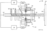
도 1은 본 발명의 코팅을 적용하는데 사용될 수 있는 본 기술 분야에서 공지된 종류인 일종의 플라즈마 스프레이 시스템의 개략적인 횡단면도(100)이며,
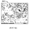
도 2a 내지 도 2c는 각각, 300배, 1000배, 및 5000배의 공지된 애스-코팅된(as-coated) 플라즈마 스프레이 이트륨 산화물 코팅의 표면에 대한 비교 현미경 사진(200,210,220)이며,
도 2d, 도 2e, 및 도 2f는 환원성 화학 플라즈마에 노출된 후 도 2a 내지 도 2c에 도시된 애스-코팅된 플라즈마 스프레이 이트륨 산화물 코팅의 표면에 대한 현미경 사진(230,240,250)으로서, 도 2d는 300배, 도 2e는 1000배, 및 도 2f는 5000배 사진이며,
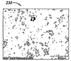
도 3a 내지 도 3c는 각각, 300배, 1000배, 및 5000배의 랩(rapped)(폴리싱) 및 애스-코팅된 플라즈마 스프레이 이트륨 산화물 코팅의 표면에 대한 현미경 사진(300,310,320)이며,
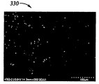
도 3d, 도 3e, 및 도 3f는 환원성 화학 플라즈마에 노출된 후 도 3a 내지 도 3c에 도시된 랩(폴리싱)된 스프레이 이트륨 산화물 코팅의 표면에 대한 현미경 사진(330,340,350)으로서, 도 3d는 300배, 도 3e는 1000배, 및 도 3f는 5000배 현미경사진이며,
도 4a는 본 발명 이전의 이용가능한 기술을 사용하여 생성된 애스-코팅된 플라즈마 스프레이 이트륨 산화물 코팅의 표면을 따라 중심선(410)으로부터 미크론 단위의 표면 거칠기의 범위를 나타내는 그래프(400)를 도시하는 비교 예이며,
도 4b는 본 발명에 따른 실시예의 기술을 사용하여 생성된 표면을 따라 중심선(430)으로부터 미크론 단위의 표면 거칠기의 범위를 나타내는 그래프(420)이며,
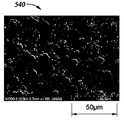
도 5a 및 도 5b는 각각, 200배 및 1000배의 본 발명 이전의 플라즈마 스프레이 기술을 사용하여 준비된 플라즈마 스프레이 이트륨 산화물 코팅의 조직을 위에서 본 비교 현미경사진(510,520)이며,
도 5c 및 도 5d는 각각, 200배 및 1000배의 본 발명의 실시예에 따른 플라즈마 스프레이 기술을 사용하여 준비된 플라즈마 스프레이 이트륨 산화물 코팅의 조직을 위에서 본 현미경사진(530,540)이며,
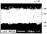
도 6a는 알루미늄 합금 기판(602)의 표면 위에 증착된 이트륨 산화물 코팅(606)을 갖는 알루미늄 합금 기판(602)을 횡단면에서 본 현미경사진(600)으로서, 200배의 본 발명 이전의 플라즈마 스프레이 기술을 사용하여 준비된 이러한 구조의 특징을 도시하는 비교 현미경사진이며,
도 6b는 알루미늄 합금 기판(612)의 표면(614) 위에 증착된 이트륨 산화물 코팅(616)을 갖는 알루미늄 합금 기판(612)을 횡단면에서 본 현미경사진(610)으로서, 200배의 본 발명에 따른 실시예인 플라즈마 스프레이 기술을 사용하여 준비된 이러한 구조의 특징을 도시하는 현미경사진이며,
도 7a는 종래의 스프레이 코팅 기술을 사용하여 도포된 (알루미늄 합금 기판 위의)플라즈마 스프레이 이트륨 산화물 코팅용 부식률을 이트륨 산화물(706)의 벌크 기판용 부식률 및 본 발명의 실시예를 사용하여 도포된 (알루미늄 기판 위의)플라즈마 스프레이 이트륨 산화물 코팅용 부식률과 비교하는 블록 다이어그램이며, 여기서 이들 테스트 시편 기판 각각은 환원 종을 함유하는 등가한 플라즈마에 노출되었으며,
도 7b는 일련의 벌크, 소결 재료들에 대한 부식률을 비교하는 블록 다이어그램(720)이며, 여기서 이들 테스트 시편 기판 각각은 환원 종을 함유하는 등가한 플라즈마에 노출되었으며,
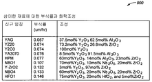
도 8은 부식률이 도 7b에 제시되어 있는 다양한 벌크 재료들에 대한 비교 결과를 요약한 테이블(800)이며,
도 9는 테이블(800)에 요약된 대부분의 재료들을 나타내는 상태도(900)이다.1 is a schematic
2A-2C are
2D, 2E, and 2F are micrographs 230,240,250 of the surface of the as-coated plasma spray yttrium oxide coating shown in FIGS. 2A-2C after exposure to a reducing chemical plasma, FIG. 2D being 300 times 2E is 1000 times, and FIG. 2F is 5000 times photograph,
3A-3C are micrographs (300,310,320) of the surface of 300 times, 1000 times, and 5000 times of rapped (polished) and as-coated plasma spray yttrium oxide coatings, respectively,
3D, 3E, and 3F are micrographs (330, 340, 350) of the surface of the wrapped (polished) spray yttrium oxide coating shown in FIGS. 3A-3C after exposure to a reducing chemical plasma, FIG. 3D being 300 times 3E is 1000 times, and FIG. 3F is 5000 times micrograph,
4A is a comparison showing a
4B is a
5A and 5B are comparative micrographs (510, 520) seen from above of the tissue of the plasma spray yttrium oxide coating prepared using the plasma spray technology prior to the present invention at 200 and 1000 times, respectively,
5C and 5D are
6A is a
FIG. 6B is a
FIG. 7A shows a corrosion rate for plasma spray yttrium oxide coating (on an aluminum alloy substrate) applied using a conventional spray coating technique using the corrosion rate for a bulk substrate of
FIG. 7B is a block diagram 720 comparing the corrosion rates for a series of bulk, sintered materials, where each of these test specimen substrates was exposed to an equivalent plasma containing reducing species,
FIG. 8 is a table 800 summarizing comparison results for various bulk materials whose corrosion rates are presented in FIG. 7B,
9 is a state diagram 900 illustrating most of the materials summarized in the table 800.
상세한 설명에 앞서, 상세한 설명 및 특허청구범위에 사용된 바와 같은, 단수 형태의 관사들은 달리 명확히 언급하지 않는 한 복수의 관련 내용을 포함한다는 것에 주의해야 한다.Prior to the description, it should be noted that articles in the singular form, as used in the description and claims, include plural related contents unless expressly stated otherwise.
용어 "약"이 본 발명에 사용된 경우에, 이 용어는 제시된 그 수치의 ±10% 이내에 있음을 의미하는 것이다.When the term "about" is used in the present invention, it is meant that it is within ± 10% of its numerical value given.
이해를 촉진시키기 위해, 도면에서 공통인 등가한 구성 요소를 지칭하는데 가능한 한 등가한 참조 부호가 사용되었다. 일 실시예의 구성 요소와 특징들은 추가의 언급 없이도 다른 실시예와 유리하게 결합될 수 있다고 이해해야 한다. 첨부 도면들은 실시예를 이해하는데 특히 도움을 줄 수 있는, 단지 본 발명의 예시적인 실시예만을 도시한 것으로 이해해야 한다. 모든 실시예들을 이해하는데 도면이 필요로 하지 않으므로, 도면들은 본 발명의 범주를 한정하는 것으로 이해해서는 안 되며 다른 균등한 유효한 실시예들이 있을 수 있다고 이해해야 한다.In order to facilitate understanding, equivalent reference numerals have been used wherever possible to refer to equivalent components that are common in the figures. It is to be understood that the components and features of one embodiment may be advantageously combined with other embodiments without further recitation. It is to be understood that the accompanying drawings illustrate only exemplary embodiments of the invention, which may be particularly helpful in understanding the embodiments. Since drawings are not required to understand all embodiments, it should be understood that the drawings are not to be construed as limiting the scope of the present invention and that there may be other equivalent effective embodiments.
전술한 바와 같이, 미립자들은 고 부식 환경에서의 반도체 소자 처리 중에 문제가 됨이 관찰되었다. 실험적으로 생성된 데이터에 의해 챔버 내 다양한 반도체 장치 처리 표면을 보호하는데 사용되는 세라믹 보호 코팅이 미립자의 대량 공급원이라는 것을 밝혀냈다. 또한, 부식률을 다양한 반도체 처리 플라즈마에 대해 비교했을 때, 플라즈마가 환원 종, 특히 수소를 포함하는 환원성 플라즈마였을 때, 미립자의 생성이 증가한다는 것이 분명해졌다.As mentioned above, fine particles have been observed to be problematic during semiconductor device processing in high corrosive environments. Experimental data have shown that the ceramic protective coatings used to protect the various semiconductor device processing surfaces in the chamber are a large source of particulates. It was also evident that when the corrosion rate was compared for various semiconductor treated plasmas, the generation of particulates increased when the plasma was a reducing plasma comprising reducing species, in particular hydrogen.
제조 공정 당 반도체 소자의 수율은 소자의 크기가 더 작아짐에 따라 그리고 반도체 기판 표면 상의 미립자의 존재가 반도체 소자의 기능과 관련하여 더욱 중요해짐에 따라 감소되었다. 반도체 처리 장치 표면을 보호하는데 사용된 코팅에 의한 미립자 생성을 감소시키기 위한 프로그램이 시작되었다.The yield of semiconductor devices per fabrication process has decreased as the size of the device becomes smaller and as the presence of particulates on the surface of the semiconductor substrate becomes more important with respect to the function of the semiconductor device. A program has been initiated to reduce particulate generation by coatings used to protect semiconductor processing device surfaces.
발전된 프로그램은 이트륨 함유 세라믹을 기초로 했다. 이들 이트륨 함유 세라믹에는 특별한 기계적 전기적 특성들을 제공하도록 설계된 더욱 특이한 다른 이트륨 함유 세라믹 재료 이외에도, 이트륨 산화물, Y2O3-ZrO2 고용체, YAG, 및 YF3가 포함된다.The developed program was based on yttrium-containing ceramics. These yttrium containing ceramics include yttrium oxide, Y 2 O 3 —ZrO 2 solid solution, YAG, and YF 3 in addition to other more specific yttrium containing ceramic materials designed to provide special mechanical and electrical properties.
도 1은 본 발명의 코팅을 적용하는데 유용한 플라즈마 스프레이 시스템의 한 형태를 개략적으로 도시하는 횡단면도(100)이다. 도 1에 도시한 특정 장치는 일본 도쿄 소재의 에어로플라즈마 가부시끼 가이샤로부터 이용 가능한 APS 7000 시리즈 에어로플라즈마 스프레이 시스템이다. 상기 장치(100)는 다음과 같은 구성 요소, 즉 제 1 DC 주 전극(102), 제 1 보조 전극(104), 제 1 아르곤 소오스(106), 제 1 공기 소오스(108), 스프레이 재료 전력 공급원(110), 캐소스 토치(112), 가속기 노즐(114), 플라즈마 아크(116), 제 2 DC 주 전극(118), 제 2 보조 전극(120), 애노드 토치(122), 스프레이 베이스 재료 소오스(124), 제 2 아르곤 소오스(126), 제 2 공기 소오스(플라즈마 트리밍)(128;128A,128B)), 스프레이 필름(130), 플라즈마 제트(132), 용융 분말 소오스(134), 제 3 아르곤 소오스(136), 및 트윈 애노드 알파 토치(138)를 포함한다.1 is a
트윈 애노드 알파 토치(138)는 두 개의 애노드 토치로 구성되어서, 각각의 애노드 토치가 열 부하의 반을 부담한다. 트윈 애노드 알파 토치(138)를 사용하여, 상당히 낮은 전류로 고전압을 얻을 수 있음으로써, 각각의 토치에 대한 열 부하가 낮아질 것이다. 토치들의 각각의 노즐과 전극은 별도로 수냉되며, 아크 시작점과 끝점이 불활성 가스에 의해 보호되어서, 200 시간 또는 그보다 많은 시간 동안 안정한 작동(200)이 보장되며, 소모 부품에 대한 수명이 연장되어 보수 유지 비용이 감소된다.Twin
안정한 고온 아크가 캐소드 토치(112)와 애노드 토치(122) 사이에 형성되며, 스프레이 재료가 아크로 직접 공급될 수 있다. 스프레이 재료가 고온 아크 칼럼에 의해 완전히 용융된다. 아크 시작점과 끝점은 불활성 가스에 의해 보호되어서, 공기 또는 산소가 가속기 노즐(114)을 통해 도입되는 플라즈마 가스용으로 사용될 수 있다.A stable high temperature arc is formed between the
플라즈마 트리밍 기능(128)이 트윈 애노드 알파에 대해 사용된다. 플라즈마 트리밍은 스프레이 재료의 용융에 기여하지 못하는 플라즈마 제트의 열을 트리밍하여 가능한 한 짧은 거리로 스프레이하도록 기판 재료와 필름 상의 열 부하를 감소시킨다.Plasma trimming function 128 is used for the twin anode alpha. Plasma trimming reduces the heat load on the substrate material and the film to trim the heat of the plasma jet that does not contribute to the melting of the spray material to spray it as short a distance as possible.
도 1에 한 종류의 플라즈마 스프레이 코팅 장치가 도시되었지만, 본 기술 분야의 당업자들은 본 발명을 수행하는데 다른 종류의 코팅 장치도 사용될 수 있다고 인정할 것이다. 본 발명에서 계속해서 제시되는 정보에 대한 이해로, 플라즈마 스프레이 코팅 및 화염 스프레이 코팅 분야의 당업자들은 최소 실험만으로도 다양한 코팅 증착 장비를 사용하여 본 발명을 수행할 수 있다.Although one type of plasma spray coating apparatus is shown in FIG. 1, those skilled in the art will recognize that other types of coating apparatus may be used to carry out the present invention. With an understanding of the information presented further in the present invention, those skilled in the art of plasma spray coatings and flame spray coatings can perform the present invention using a variety of coating deposition equipment with minimal experimentation.
도 2a, 도 2b 및 도 2c는 본 발명의 선행 기술을 사용하여 증착된 약 200 ㎛ 두께를 갖는 애스-코팅된 플라즈마 스프레이 이트륨 산화물 코팅의 상부면에 대한 비교 현미경사진(200,210,220)을 나타낸다. 상기 현미경사진들은 각각, 300배, 1000배, 및 5000배 사진이다. 직접 미립자를 형성할 수 있는 벗겨지기 쉬운 표면 조직은 상기 배율에서 모두 명확히 나타나나, 특히 5000 배율에서 특히 명확하다.2A, 2B and 2C show
도 2d, 도 2e 및 도 2f는 환원성 화학물 플라즈마에 노출된 후 도 2a 내지 도 2c에 도시된 애스-코팅된 플라즈마 스프레이 이트륨 산화물 코팅의 표면에 대한 현미경사진(230,240,250)을 나타낸다. 도 2d는 300배, 도 2e는 1000배, 그리고 도 2f는 5000배 사진이다. 미국 캘리포니아 산타 클라라 소재의 어플라이드 머티리얼즈 인코포레이티드로부터 이용 가능한 종류의 300 mm eMax(등록상표) CT+ 챔버에서의 도 2, 도 3 및 도 7b의 데이터에 대한 환원 플라즈마 레시피를 표 1에 나타냈다. 평가된 테스트 시편 기판이 웨이퍼 위에 위치된 후에 처리 챔버 내의 ESC 위치에 넣어졌다. 도 2a, 도 2b 및 도 2c에 도시된 대량의 벗겨지기 쉬운 조직이 환원 플라즈마에 노출 중에 제거되었다. 제거된 재료는 환원성 화학물 플라즈마를 사용하여 처리된 소자를 포함하는 반도체 구조물의 표면 상에 나타나는 미립자일 것이다.
2D, 2E and 2F show micrographs 230,240 and 250 of the surface of the as-coated plasma spray yttrium oxide coating shown in FIGS. 2A-2C after exposure to reducing chemical plasma. FIG. 2D is 300 times, FIG. 2E is 1000 times, and FIG. 2F is a 5000 times picture. Table 1 shows the reduction plasma recipe for the data of FIGS. 2, 3 and 7B in a 300 mm eMax® CT + chamber of the kind available from Applied Materials, Inc. of Santa Clara, California. The evaluated test specimen substrate was placed on the wafer and then placed in the ESC position in the processing chamber. The large amount of flaky tissue shown in FIGS. 2A, 2B and 2C was removed during exposure to the reducing plasma. The material removed will be particulates that appear on the surface of the semiconductor structure including the device treated using a reducing chemical plasma.
HRF
H
LRF
L
SRF
S
fldB
fld
* 완전 개방* Fully Open
전술한 처리 레시피에 노출되는 동안 기판 온도는 약 25℃였다.
The substrate temperature was about 25 [deg.] C. while exposed to the treatment recipe described above.
도시된 도 2c와 도 2f를 비교함으로써 플라즈마에 노출 중에 이트륨 산화물 코팅 표면으로부터 벗겨지기 쉬운 조직이 제거되었음을 쉽게 알 수 있다. 이는 처리된 반도체 소자 표면 상에서 발견되는 미립자의 화학 조성과 관련하여 벌크 미립자들이 이트륨 산화물 코팅으로부터 생성되었음을 확인되었다.By comparing FIG. 2C with FIG. 2F shown, it can be readily seen that the flaky tissue was removed from the yttrium oxide coating surface during exposure to the plasma. It was confirmed that bulk particles were produced from the yttrium oxide coating in relation to the chemical composition of the particles found on the treated semiconductor device surface.
코팅 두께의 깊이가 증가함에 따른 스프레이 코팅 이트륨 산화물 층의 실험에 따른 연구에 의해 이트륨 산화물의 전체 결정질 조직과 이트륨 산화물 코팅의 다공도가 코팅 두께에 걸쳐 상당히 일정하다는 것이 밝혀졌다. 그러나, 도시된 도 2a 내지 도 2c를 도 2d 내지 도 2f와 비교함으로써, 반도체 소자를 제조하기 위한 반도체 코팅 장치를 사용하기 이전에 애스-코팅 장치의 벗겨지기 쉬운 상부 표면을 제거하는 것에 의해 신규한 코팅 장치가 처리 챔버 내측으로 도입될 때인 초기의 심각한 미립자 생성 시기를 피하는 것이 가능하다.Experimental studies of spray coated yttrium oxide layers as the depth of the coating thickness increased have found that the overall crystalline structure of the yttrium oxide and the porosity of the yttrium oxide coating are fairly constant over the coating thickness. However, by comparing the depicted FIGS. 2A-2C with FIGS. 2D-2F, the novel method is achieved by removing the flaky top surface of the as-coating apparatus prior to using the semiconductor coating apparatus for manufacturing the semiconductor device. It is possible to avoid the initial severe particulate generation timing, which is when the coating apparatus is introduced into the processing chamber.
벗겨지기 쉬운 상부 표면은 도 2d 내지 도 2f를 참조하여 설명한 극도의 환원성 플라즈마에 노출함으로써 제거될 수 있다. 그러나, 이는 플라즈마에 대략 50시간의 노출을 필요로 함으로써 실용적이지 못하다. 대신에, 이트륨 산화물 플라즈마 스프레이 코팅 장치의 표면이 세라믹 재료의 폴리싱을 위한 기술 분야에서 일반적으로 공지된 랩핑(lapping) 기술을 사용하여 폴리싱되었다. 도 3a 내지 도 3c는 각각, 300배, 1000배 및 5000배의 래핑되고(폴리싱되고) 애스-코팅된 플라즈마 스프레이 이트륨 산화물 코팅의 표면에 대한 현미경사진(300,310,320)이다. 벗겨지기 쉬운 재료가 코팅의 상부 표면으로부터 제거되었음을 쉽게 알 수 있다.The flaky top surface can be removed by exposure to the extreme reducing plasma described with reference to FIGS. 2D-2F. However, this is not practical by requiring approximately 50 hours of exposure to the plasma. Instead, the surface of the yttrium oxide plasma spray coating apparatus was polished using a lapping technique generally known in the art for polishing ceramic materials. 3A-3C are micrographs 300,310, and 320 of the surface of the wrapped (polished) as-coated plasma spray yttrium oxide coating of 300, 1000, and 5000 times, respectively. It can be readily seen that the flaky material has been removed from the top surface of the coating.
도 3d 내지 도 3f는 도 3a 내지 도 3c에 도시된 랩핑된(폴리싱된) 플라즈마 스프레이 이트륨 산화물 코팅의 표면에 대한 현미경사진(330,340,350)이다. 도 3d는 300배이며, 도 3e는 1000배이며, 도 3f는 5000배이다. 환원성 플라즈마는 표 1에 나타낸 방법으로 생성되었다. 노출 시간은 50 시간이었다. 벗겨지기 쉬운 조직이 도시된 도 3c를 도 3f와 비교함으로써 노출 중에 이트륨 산화물 코팅 표면으로부터 제거됨을 쉽게 알 수 있다. 그러나, 도 3f로부터 알 수 있는 바와 같이, 부식 환경에서 처리 시간에 걸쳐 노출된 코팅 표면은 (이트륨 산화물의 보호 층에 대해 점진적인 부식이 발생하기 때문에)코팅 표면 내의 크랙과 스프레이 코팅된 세라믹 재료의 전반적인 입계 조직으로 인해 미립자 형성에 아주 상당히 민감하다. 조밀하고 기공이 감소된 보디 조직 및 부드럽고 조밀한 코팅 표면을 제공하기 위한 스프레이 코팅된 이트륨 산화물의 추가 개선은 미립자 생성의 감소에 도움이 될 것이다.3D-3F are
본 발명의 다른 실시예는 환원성 플라즈마에 의한 침식에 덜 민감한 더욱 조밀한 스프레이 코팅을 얻기 위한 스프레이 코팅 기술의 개선에 관한 것이다. 플라즈마 스프레이 코팅 공정의 다양한 변수들이 실험된 상당한 실험 이후에, 알루미늄 합금 기판에 코팅을 도포하는데 사용되었던 플라즈마 스프레이 코팅 장치로 공급되는 보다 작은 크기의 이트륨 산화물 분말의 사용에 의해 스프레이 코팅된 이트륨 산화물 표면의 다공도와 표면 거칠기에 있어서 예상치 못한 상당한 감소가 달성되었다.Another embodiment of the present invention is directed to an improvement in spray coating technology to obtain a more dense spray coating that is less susceptible to erosion by reducing plasma. After considerable experiments where various parameters of the plasma spray coating process were tested, the surface of the yttrium oxide surface sprayed by the use of smaller sized yttrium oxide powder supplied to the plasma spray coating apparatus that was used to apply the coating to the aluminum alloy substrate. An unexpected and significant reduction in porosity and surface roughness was achieved.
예를 들어, 본 발명 이전의 플라즈마 스프레이 코팅 장치로 공급되었던 이트륨 산화물 분말의 종래의 평균적인 유효 입자 직경은 25 ㎛ 이상이었다. 실험적 데이터에 의해 이러한 평균 분말 직경의 약 22 ㎛ 또는 그 미만, 통상적으로 약 15 ㎛ 내지 약 0.1 ㎛으로의 감소는 알루미늄 합금 기판 표면 상에 생성된 이트륨 산화물 코팅의 다공도를 상당히 감소시켰음을 알 수 있다.For example, the conventional average effective particle diameter of the yttrium oxide powder supplied to the plasma spray coating apparatus prior to the present invention was 25 μm or more. Experimental data show that a reduction of this average powder diameter to about 22 μm or less, typically from about 15 μm to about 0.1 μm, significantly reduced the porosity of the yttrium oxide coating produced on the aluminum alloy substrate surface. .
아래의 표 2는 플라즈마 스프레이 이트륨 산화물 코팅의 물리적 특징들의 개선을 나타내는데, 이러한 특징들의 개선은 플라즈마 스프레이 코팅 장치로 공급되는 이트륨 산화물 분말의 크기를 전술한 방법으로 변경시킨 본 발명의 실시예들을 사용하여 달성되었다.
Table 2 below shows the improvement of the physical characteristics of the plasma spray yttrium oxide coating, which improvement was carried out using the embodiments of the present invention in which the size of the yttrium oxide powder supplied to the plasma spray coating apparatus was changed by the method described above. Was achieved.
증착기술coating
Deposition technology
거칠기(Ra)Coated surface
Roughness Ra
테스트*HCl Bubble
Test*
실시예The present invention
Example
*버블 테스트은 반도체 기술에서 일반적으로 공지된 어플라이드 머티리얼즈 기술 편람, 파트 번호 0250-39691로 수행되었다. 현재, 이 실험의 실패 기준은 연속 기준으로 초 당 4 수소 기포의 출현이다.The bubble test was performed with the Applied Materials Technology Handbook, Part No. 0250-39691, generally known in semiconductor technology. Currently, the failure criterion for this experiment is the appearance of 4 hydrogen bubbles per second on a continuous basis.
**이트륨 산화물 코팅의 체적 다공도는 코팅의 표면에 대한 현미경사진에 적용된 (미국 메릴랜드 베데스다 소재의 메디아 사이버네틱스로부터 이용가능한)이미지-프로 플러스, 버전 6.0을 사용하여 측정되었다.** Volume porosity of the yttrium oxide coating was measured using Image-Pro Plus, version 6.0 (available from Media Cybernetics, Bethesda, MD) applied to micrographs of the surface of the coating.
***경도는 비커스 경도(Hv) 실험을 사용하여 측정되었으며, Hv 값은 ASTM E92-82에 기초하여 계산되었다.
*** Hardness was measured using Vickers hardness (Hv) experiments and Hv values were calculated based on ASTM E92-82.
표 2에서 설명한 바와 같이, 200 ㎛ 두께의 코팅에 대해 종래의 25 ㎛ 직경의 이트륨 산화물 분말을 사용하여 생성된 이트륨 산화물 코팅의 평균 다공도는 약 1.5 % 내지 약 4 % 범위인 반면에, 크기가 감소된 동등한 직경 크기의 이트륨 산화물 분말을 사용하여 생성된 이트륨 산화물 코팅의 평균 다공도는 약 1.5% 미만으로부터 약 0.15%로 감소되었다. 예로서, 15 ㎛의 동등한 직경의 분말은 약 0.47%의 다공도를 갖는 코팅을 생성했다. 이와 같은 다공도의 감소는 환원 종을 함유하는 플라즈마의 침식 용이성을 나타내는 지표로서 특히 중요하다. 또한, 종래의 25 ㎛ 직경의 분말을 사용하여 생성된 이트륨 산화물의 평균 표면 거칠기(Ra)는 플라즈마 스프레이 코팅 장치로 공급되는 크기가 감소된 15 ㎛ 직경의 이트륨 산화물 분말을 사용하여 생성된 이트륨 산화물 코팅에 대한 단지 51.2 μ-인치 Ra(1.28 ㎛ Ra)의 평균 표면 거칠기와 비교하여 약 200 μ-인치 Ra(5.0 ㎛ Ra)였다. 표준 HCl 버블 테스트을 사용하여, 종래의 25 ㎛ 동등한 직경 분말을 사용하여 생성된 200 ㎛ 두께의 이트륨 산화물에 대해 약 7.5 내지 8 시간 동안 수행된 반면에, 크기가 감소된 15 ㎛ 직경 분말을 사용하여 생성된 200 ㎛ 두께의 이트륨 산화물 코팅은 10 시간을 초과하는 시간 주기 동안 수행되었다. 또한, 종래의 25 ㎛ 동등한 직경 분말을 사용하여 생성된 상기 이트륨 산화물에 대한 파괴 전압(VBD)은 단지 750 V/mil인 반면에, 크기가 감소된 15 ㎛ 직경 분말을 사용하여 생성된 상기 이트륨 산화물 코팅에 대한 파괴 전압은 875 V/mil였다. 본 기술 분야의 당업자들은 이트륨 함유 코팅의 스프레이 코팅을 위해 산업 분야에 일반적으로 사용되는 임의의 장치를 사용할 수 있으며 최소 실험으로 유사한 상대적인 결과를 얻을 수 있다.As described in Table 2, the average porosity of the yttrium oxide coating produced using a conventional 25 μm diameter yttrium oxide powder for a 200 μm thick coating ranged from about 1.5% to about 4%, while the size was reduced. The average porosity of the yttrium oxide coating produced using the equivalent diameter sized yttrium oxide powder was reduced from less than about 1.5% to about 0.15%. As an example, an equivalent diameter powder of 15 μm produced a coating having a porosity of about 0.47%. This reduction in porosity is particularly important as an indicator of the erosion ease of plasma containing reducing species. In addition, the average surface roughness (Ra) of yttrium oxide produced using a conventional 25 μm diameter powder was obtained by using a yttrium oxide powder having a reduced size of 15 μm diameter yttrium oxide powder supplied to a plasma spray coating apparatus. It was about 200 μ-inch Ra (5.0 μm Ra) compared to the average surface roughness of only 51.2 μ-inch Ra (1.28 μm Ra) for. Using a standard HCl bubble test, it was performed for about 7.5 to 8 hours on 200 μm thick yttrium oxide produced using a conventional 25 μm equivalent diameter powder, while using a reduced
도 4a는 본 발명 이전에 이용가능한 기술을 사용하여 생성된 애스-코팅된 플라즈마 스프레이 이트륨 산화물 코팅의 표면을 따라 중심선(410)으로부터 μ 단위의 표면 거칠기 범위를 나타내는 그래프(400)이다. 표면을 따른 이동 거리는 축선(402) 상의 밀리미터 단위로 나타낸 반면에, 중심선 아래의 깊이 또는 중심선 위의 높이는 축선(404) 상에 μ 단위 범위로 나타냈다. 상기 범위의 중심선으로부터의 표면 거리는 약 + 23 μ 내지 약 - 17 μ 범위였다.4A is a
도 4b는 애스-코팅된 플라즈마 스프레이 이트륨 산화물 코팅의 표면을 따른 중심선(430)으로부터 표면 거칠기의 범위를 μ단위로 나타낸 그래프(420)이다. 플라즈마 스프레이 코팅은 감소된 유효 직경의 분말이 플라즈마 스프레이 장치로 공급되는 본 발명의 실시예를 사용하여 제조되었다. 표면을 따라 이동된 거리는 축선(422) 상에 밀리미터 단위로 나타낸 반면에, 상기 범위의 중심선 아래 깊이 또는 중심선 위의 높이는 축선(424) 상에 μ 단위로 나타냈다. 중심선으로부터의 표면 거리는 약 + 6 μ 내지 약 - 4.5 μ 범위였다. 높이 및 깊이의 표면 편차 범위에서의 이러한 상당한 변동은 부식성 환원 플라즈마에 노출된 보호 코팅의 표면적을 실질적으로 감소시킨다.4B is a
도 5a 및 도 5b는 각각, 200배 및 1000배의 본 발명 이전의 플라즈마 스프레이 기술을 사용하여 준비된 플라즈마 스프레이 이트륨 산화물 코팅의 조직을 위에서 본 비교 현미경 사진(510,520)이다. 도 5c 및 도 5d는 감소된 유효 직경의 분말이 플라즈마 스프레이 장치로 공급되는 본 발명의 실시예를 사용하여 준비된 플라즈마 스프레이 이트륨 산화물 코팅의 조직을 위에서 본 현미경 사진(530,540)이다. 도 5c 및 도 5d는 각각 200배 및 1000배 사진이다. 도 5a 및 도 5b를 도 5c 및 도 5d와의 비교로 플라즈마에 의해 침식된 표면적이 감소되었음을 알 수 있다. 도 5a 및 도 5b의 표면 조직은 환원성 플라즈마에 의해 (도 5c 및 도 5d의 표면 조직에 비해)더욱 침식받기 쉽다는 것을 나타내는데, 이는 표면의 높이 및 깊이에 있어서 수직 변동에 의해 2차원 방향으로의 노출 증가뿐만 아니라, 코팅 표면 위로 연장하는 구형 구조물로 인한 표면적의 증가에 의한 것이다.5A and 5B are
도 6a는 알루미늄 합금 기판(602)의 표면(604) 위에 증착된 이트륨 산화물 코팅(606)을 갖는 알루미늄 합금 기판(602)의 횡단면도를 나타내는 비교 현미경사진(600)이다. 이러한 비교 현미경 사진은 약 200 ㎛ 두께를 갖는 이트륨 산화물 코팅을 생성하기 위해, 본 발명 이전의 플라즈마 스프레이 기술을 사용하여 준비된 구조물의 특징들을 나타낸다. 현미경 사진의 배율은 200배이다. 상기 실험 시편의 알루미늄 합금 기판(602)은 현미경사진(600)의 기저부에 나타나 있다. 알루미늄 합금의 표면(604)의 거칠기는 명확히 한정되어 있다. 스프레이 코팅된 이트륨 산화물(606)의 전체 다공도도 종래의 25 ㎛의 평균 유효 직경의 이트륨 산화물 분말이 플라즈마 스프레이 코팅 장치로 공급되는 종래 기술의 플라즈마 스프레이 기술을 사용하여 준비된 코팅의 표면(608) 거칠기와 같이, 식별가능하다.6A is a
도 6b는 감소된 유효 직경 분말의 이트륨 산화물이 플라즈마 스프레이어로 공급될 때 달성되는 플라즈마 스프레이 코팅된 이트륨 산화물 코팅에서의 개선을 나타내는 현미경사진(610)이다. 도 6b는 알루미늄 합금 기판의 표면(614) 위에 증착된 이트륨 산화물 코팅(616)을 갖는 알루미늄 합금 기판(612)의 횡단면도이다. 또한, 그 배율은 200배이다. 실험 시편의 알루미늄 합금 기판(612)은 현미경사진(61)의 기저부에 도시되어 있다. 알루미늄 합금의 표면(614)의 거칠기도 명확히 한정되어 있으며, 도 6a에 도시된 것과 유사하다. 스프레이 코팅된 이트륨 산화물(616)의 전체 다공도는 도 6a에 도시된 종래 기술의 공정을 사용하여 준비된 코팅에 대한 것보다 상당히 작아졌다. 본 발명의 실시예를 사용하여 준비된 코팅의 표면(618) 거칠기는 종래 기술의 플라즈마 스프레이 기술을 사용하여 생성된 것보다 훨씬 더 부드럽다. 현미경사진(600,610)은 표 2에 포함된 데이터를 추가로 지지한다.6B is a
도 7a는 다양한 이트륨 산화물 함유 기판들에 대한 부식률을 비교하는 블록 다이어그램(700)이다. 각각의 이트륨 산화물 함유 기판에 대한 부식률은 블록 다이어그램(700)의 축선(702)에 ㎛/시간의 단위로 도시되어 있다. 블록(704)은 25 ㎛ 또는 그보다 큰 평균 유효 입자 직경을 갖는 사용된 이트륨 산화물 미립자들이 플라즈마 스프레이 장치로 공급되는 선행 스프레이 코팅 방법을 사용하여 (알루미늄 합금 기판 위에)도포되는 플라즈마 스프레이 이트륨 산화물 코팅에 대한 부식률을 나타낸다. 블록(706)은 이트륨 산화물(706)의 (본 기술분야에서 이미 공지된 종류의)벌크 시편 기판에 대한 부식률을 나타낸다. 블록(708)은 (알루미늄 기판 위에)플라즈마 스프레이 이트륨 산화물 코팅에 대한 부식을 나타내며, 여기서 플라즈마 스프레이 장치로 공급되는 감소된 분말 입자크기의 이트륨 산화물을 사용하는 본 발명의 실시예를 사용하여 이트륨 산화물 코팅이 도포되었다. 각각의 실험 기판은 환원성 종을 함유하는 등가한 플라즈마에 노출되었다. 도 7a에 도시된 데이터를 생성하는데 사용된 플라즈마 처리 레시피가 아래의 표 3에 제시되어 있다. 처리 중의 평균 온도는 처리 단계에 따라 약 20 ℃ 내지 약 90 ℃ 범위이다. 플라즈마에 대한 노출 시간 주기는 87 시간이었다. 플라즈마 스프레이 장치로 공급되는 감소된 분말 크기의 이트륨 산화물을 사용하여 생성된 종류의 스프레이 코팅된 이트륨 산화물 처리 성분이 고체 이트륨 산화물 성분보다 더 적은 미립자를 생성했다고 판단했다. 이는 고체 이트륨 산화물 성분이 소결 첨가제 사용을 필요한다는 사실에 기인하다고 생각된다. 입계 유리질 상을 생성하는 소결 첨가제의 사용은 미립자 형성의 근원이다.
7A is a block diagram 700 comparing the corrosion rates for various yttrium oxide containing substrates. The corrosion rate for each yttrium oxide containing substrate is shown on the
전력bias
power
전력Source
power
인/아웃**CSTU
In / Out **
인/아웃***He
In / Out ***
*NSTU : 중립 시편 튜닝 유닛(비율).NSTU: Neutral Specimen Tuning Unit (ratio).
**CSTU : 변경 시편 튜닝 유닛(암페어).** CSTU: Modified Specimen Tuning Unit (Amps).
***기판 지지 플랫폼으로, 지지 플랫폼 표면에서 내측 유체 순환 링으로 그리고 외측 유체 순환 링으로 헬륨 냉각제가 공급됨.
*** With substrate support platform, helium coolant is supplied from the support platform surface to the inner fluid circulation ring and to the outer fluid circulation ring.
도 7b는 각각 다른 화학 조성을 갖는 일련의 벌크 재료에 대한 부식률을 비교하는 블록 다이어그램(720)이다. 이들 실험 시편 각각은 300 mm eMax CT+ 처리 챔버 내에서 표 1에 제시한 레시피에 따라 환원성 시편을 함유하는 등가한 플라즈마에 노출되었다. YAG 벌크 재료에 대한 실험의 수행으로 내식성을 개선하는 방법으로서 환원성 플라즈마로 Y(OH)3의 형성을 방지하는 것에 관한 이론을 확인했다. 블록(724)은 HFO1 기판을 나타내며, 블록(726)은 NB04 기판을 나타내며, 블록(728)은 Y-ZrO2 기판을 나타내며, 블록(730)은 NB01 기판을 나타내며, 블록(732)는 HPM 기판을 나타내며, 블록(734)는 YA3070 기판을 나타내며, 블록(736)은 Y2O3 기판을 나타내며, 블록(738)은 YZ20을 나타내며, 블록(740)은 YAG 기판을 나타낸다. 블록(736,738,740)은 이것들이 각각 Y2O3, 20 원자%의 ZrO2를 함유하는 Y2O3-ZrO2, 및 YAG를 위한 벌크 기판을 대표하기 때문에 가장 흥미롭다. 이들 3 개의 재료는 본 발명의 실시예들 중 하나에 따라 플라즈마 스프레이 코팅에 적용될 때 환원성 플라즈마에 대한 특별한 저항력을 나타낸다.7B is a block diagram 720 comparing the corrosion rates for a series of bulk materials, each having a different chemical composition. Each of these test specimens was exposed to an equivalent plasma containing reducing specimens according to the recipes presented in Table 1 in a 300 mm eMax CT + treatment chamber. Experiments on YAG bulk materials confirmed the theory of preventing the formation of Y (OH) 3 with reducing plasma as a method of improving the corrosion resistance.
도 8은 도 7b에 부식률을 나타낸 다양한 벌크 재료의 다양한 출발 분말에 대한 화학 조성들을 요약한 표(800)이다.FIG. 8 is a table 800 summarizing the chemical compositions for various starting powders of various bulk materials showing corrosion rates in FIG. 7B.
도 9는 재료가 표(800)에 요약되어 있는, 출발 분말의 화학 조성 및 형성된 최종 재료 내의 상들을 도시하는 상태도(900)이다.9 is a state diagram 900 showing the chemical composition of the starting powder and the phases in the final material formed, the materials of which are summarized in the table 800.
이트륨 산화물 코팅의 성능을 개선하기 위한 작업 중에, 이트륨 산화물 표면에 대한 침식 메카니즘이 이트륨 수산화물[Y(OH)3]의 형성을 통해 발견되었다. 수소와 산소의 반응성 플라즈마 종이 존재하면, Y(OH)3 화합물이 형성된다. 수소, 불소 및 산소의 플라즈마 종이 존재하면, Y(OH)3 화합물이 형성된다. 이론적으로, 다양한 화합물에 대한 열역학적 데이터(깁스의 형성 자유 에너지)를 검토함으로써, Y(OH)3 화합물이 형성될 가능성을 결정할 수 있다. 실험에 있어서, Y(OH)3 화합물의 형성을 검출하는데 고 해상도 XPS가 사용되었다. 일반적으로 Y3Al5O12 형태인 이트륨 알루미늄 가닛의 사용 및 Y2O3-ZrO2 고용체의 사용으로 Y(OH)3의 형성을 방지할 수 있음이 실험에 의해 밝혀졌다. 또한, YF3가 열역학적으로 안정하고 Y(OH)3의 형성에 저항함으로써 환원성 활성 종을 함유하는 플라즈마 환경에서의 보호 코팅으로서 이러한 재료의 사용이 바람직하다는 것도 추가의 연구로 알아냈다. 이와 같은 YAG, Y2O3-ZrO2 고용체, YF3, 또는 이들의 조합물이 환원성 활성 종을 포함하는 플라즈마 환경에서의 보호 코팅으로의 사용에 우수한 재료이다. 약 0.5 % 또는 그 미만 범위의 유리한 다공도 및 875 또는 그 초과의 파괴 전압(VBD)을 제공하기 위해, 플라즈마 스프레이된 YAG, Y2O3-ZrO2 고용체, YF3 코팅을 증착하는데 사용된 평균(등가 직경) 미립자 크기는 약 22 ㎛ 내지 약 5 ㎛ 범위이다. 또한, 스프레이 코팅 장치가 상기 크기의 미립자들을 취급할 수 있도록 구성되면, 크기가 약 0.1 ㎛로 감소된 등가 직경 미립자도 사용될 수 있다. 이러한 크기가 감소된 분말은 플라즈마 스프레이 코팅의 다공도를 감소시키며 플라즈마 스프레이된 Y2O3 함유 코팅에 크기 감소된 분말의 사용에서 관찰된 것과 등가한 방식으로 더욱 조밀한 구조물을 제공할 수 있다.During work to improve the performance of yttrium oxide coatings, erosion mechanisms on the yttrium oxide surface have been found through the formation of yttrium hydroxide [Y (OH) 3 ]. When a reactive plasma species of hydrogen and oxygen is present, a Y (OH) 3 compound is formed. When plasma species of hydrogen, fluorine and oxygen are present, Y (OH) 3 compounds are formed. In theory, by examining the thermodynamic data (free energy of formation of casts) for various compounds, the possibility of forming Y (OH) 3 compounds can be determined. In the experiments, high resolution XPS was used to detect the formation of Y (OH) 3 compounds. Use of yttrium aluminum garnet, usually in the form of Y 3 Al 5 O 12 and Y 2 O 3 -ZrO 2 Experiments have shown that the use of a solid solution can prevent the formation of Y (OH) 3 . It has also been found in further studies that the use of such a material as a protective coating in a plasma environment containing reducing active species is desirable by the fact that YF 3 is thermodynamically stable and resists the formation of Y (OH) 3 . Such YAG, Y 2 O 3 -ZrO 2 Solid solutions, YF 3 , or a combination thereof are excellent materials for use as a protective coating in a plasma environment comprising reducing active species. Plasma sprayed YAG, Y 2 O 3 -ZrO 2 to provide advantageous porosity in the range of about 0.5% or less and 875 or more breakdown voltage (V BD ) Solid solution, YF 3 The average (equivalent diameter) particulate size used to deposit the coating ranges from about 22 μm to about 5 μm. Also, if the spray coating apparatus is configured to handle fine particles of this size, equivalent diameter fine particles reduced in size to about 0.1 μm may also be used. This reduced powder reduces the porosity of the plasma spray coating and results in plasma sprayed Y 2 O 3 More dense structures can be provided in an equivalent manner as observed in the use of reduced size powders in the containing coating.
이상의 설명은 본 발명의 실시예에 관한 것이었지만, 본 발명의 다른 추가의 실시예들이 본 발명의 기본 범주를 벗어남이 없이 본 발명의 설명을 감안하여 창안될 수 있으며, 본 발명의 범주는 다음의 특허청구범위에 의해 결정된다.While the foregoing description has been directed to embodiments of the present invention, other additional embodiments of the invention may be devised in view of the description of the invention without departing from the basic scope thereof, and the scope of the invention is set forth in the following Determined by the claims.
Claims (17)
표면 상에 스프레이 코팅된 이트륨 함유 세라믹 재료를 갖는 금속 또는 금속 합금 기판을 포함하며,
상기 세라믹 코팅의 다공도가 1.5% 미만인,
물품.
An article having corrosion or erosion resistance to chemically active reducing plasma,
A metal or metal alloy substrate having a yttrium containing ceramic material spray coated on the surface,
The porosity of the ceramic coating is less than 1.5%,
article.
상기 다공도는 1.5% 미만 내지 약 0.1% 범위인,
물품.
The method of claim 1,
The porosity ranges from less than 1.5% to about 0.1%,
article.
상기 다공도는 약 1% 내지 약 0.1% 범위인,
물품.
The method of claim 2,
The porosity ranges from about 1% to about 0.1%,
article.
상기 스프레이 코팅된 이트륨 함유 세라믹 재료의 노출 표면은 약 3 ㎛ Ra 미만의 표면 거칠기를 가지는,
물품.
The method of claim 1,
The exposed surface of the spray coated yttrium containing ceramic material has a surface roughness of less than about 3 μm Ra
article.
상기 표면 거칠기는 약 1.5 ㎛ Ra 미만 내지 약 0.6 ㎛ Ra 범위인,
물품.
The method of claim 3, wherein
The surface roughness ranges from less than about 1.5 μm Ra to about 0.6 μm Ra,
article.
상기 스프레이 코팅된 이트륨 함유 세라믹 재료의 파괴 전압은 650 V/mil 이상인,
물품.
The method of claim 1,
The breakdown voltage of the spray coated yttrium containing ceramic material is 650 V / mil or more,
article.
상기 파괴 전압은 약 650 V/mil 내지 약 900 V/mil 이상까지의 범위인,
물품.
The method according to claim 6,
The breakdown voltage ranges from about 650 V / mil to about 900 V / mil or more;
article.
상기 스프레이 코팅된 이트륨 함유 세라믹 재료는 약 5 ㎛ 내지 약 400 ㎛ 범위의 두께를 가지는,
물품.
The method according to claim 1 or 4 or 6,
The spray coated yttrium containing ceramic material has a thickness in a range from about 5 μm to about 400 μm,
article.
상기 재료의 두께는 약 25 ㎛ 내지 약 300 ㎛ 범위인,
물품.
The method of claim 8,
Wherein the thickness of the material ranges from about 25 μm to about 300 μm,
article.
상기 이트륨 함유 세라믹 재료는 Y2O3, Y2O3-ZrO2 고용체, YAG, YF3, 또는 이들의 조합물로 이루어지는 그룹으로부터 선택되는,
물품.
The method of claim 8,
The yttrium-containing ceramic material is Y 2 O 3 , Y 2 O 3 -ZrO 2 Selected from the group consisting of solid solutions, YAG, YF 3 , or combinations thereof
article.
상기 스프레이 코팅된 이트륨 함유 세라믹 재료는 8 시간 이상의 시간 주기 동안의 HCl 버블 테스트를 통과한,
물품.
The method of claim 2,
The spray coated yttrium containing ceramic material passed the HCl bubble test for a time period of at least 8 hours,
article.
상기 스프레이 코팅된 이트륨 함유 세라믹 재료는 10 시간 이상의 시간 주기 동안의 HCl 버블 테스트를 통과한,
물품.
The method of claim 3, wherein
The spray coated yttrium containing ceramic material passed the HCl bubble test for a time period of 10 hours or more,
article.
금속 또는 금속 합금 기판 상에 이트륨 함유 세라믹 재료를 플라즈마 스프레이 코팅함으로써 상기 물품을 제조하는 단계를 포함하며,
상기 이트륨 함유 세라믹 재료는 약 22 ㎛ 내지 약 0.1 ㎛ 범위의 평균 등가 직경을 갖는 분말 형태인,
물품 제조 방법.
A method of making an article having corrosion or erosion resistance to chemically active reducing plasma,
Preparing the article by plasma spray coating a yttrium containing ceramic material on a metal or metal alloy substrate,
The yttrium containing ceramic material is in powder form with an average equivalent diameter in the range of about 22 μm to about 0.1 μm.
Method of manufacturing the article.
상기 평균 등가 직경은 약 15 ㎛ 내지 약 5 ㎛ 범위인,
물품 제조 방법.
The method of claim 13,
The average equivalent diameter ranges from about 15 μm to about 5 μm,
Method of manufacturing the article.
상기 이트륨 함유 재료는 Y2O3, Y2O3-ZrO2 고용체, YAG, YF3, 또는 이들의 조합물로 이루어지는 그룹으로부터 선택되는,
물품 제조 방법.
The method according to claim 13 or 14,
The yttrium containing material is Y 2 O 3 , Y 2 O 3 -ZrO 2 Selected from the group consisting of solid solutions, YAG, YF 3 , or combinations thereof
Method of manufacturing the article.
상기 이트륨 함유 재료는 Y2O3-ZrO2 고용체, YAG, YF3, 또는 이들의 조합물로 이루어지는 그룹으로부터 선택되는,
물품 제조 방법.
The method of claim 13,
The yttrium containing material is Y 2 O 3 -ZrO 2 Selected from the group consisting of solid solutions, YAG, YF 3 , or combinations thereof
Method of manufacturing the article.
금속 또는 금속 합금 기판 상에 이트륨 함유 세라믹 재료를 플라즈마 스프레이 코팅함으로써 상기 물품을 제조하는 단계를 포함하며,
상기 이트륨 함유 세라믹 재료는 Y2O3-ZrO2 고용체, YF3, 또는 이들의 조합물로 이루어지는 그룹으로부터 선택되는,
물품 제조 방법.A method of making an article having corrosion or erosion resistance to chemically active reducing plasma,
Preparing the article by plasma spray coating a yttrium containing ceramic material on a metal or metal alloy substrate,
The yttrium-containing ceramic material is Y 2 O 3 -ZrO 2 Selected from the group consisting of a solid solution, YF 3 , or a combination thereof,
Method of manufacturing the article.
Applications Claiming Priority (2)
| Application Number | Priority Date | Filing Date | Title |
|---|---|---|---|
| US12/072,530 | 2008-02-26 | ||
| US12/072,530 US20090214825A1 (en) | 2008-02-26 | 2008-02-26 | Ceramic coating comprising yttrium which is resistant to a reducing plasma |
Publications (1)
| Publication Number | Publication Date |
|---|---|
| KR20100118994A true KR20100118994A (en) | 2010-11-08 |
Family
ID=40998600
Family Applications (1)
| Application Number | Title | Priority Date | Filing Date |
|---|---|---|---|
| KR1020107020779A KR20100118994A (en) | 2008-02-26 | 2009-02-13 | Ceramic coating comprising yttrium which is resistant to a reducing plasma |
Country Status (7)
| Country | Link |
|---|---|
| US (1) | US20090214825A1 (en) |
| JP (1) | JP5674479B2 (en) |
| KR (1) | KR20100118994A (en) |
| CN (1) | CN102084020B (en) |
| SG (2) | SG187415A1 (en) |
| TW (1) | TWI455820B (en) |
| WO (1) | WO2009108275A2 (en) |
Cited By (2)
| Publication number | Priority date | Publication date | Assignee | Title |
|---|---|---|---|---|
| WO2018151462A1 (en) * | 2017-02-15 | 2018-08-23 | 주식회사 펨빅스 | Gas showerhead having gas flow channel with crackless coating film |
| KR102290498B1 (en) | 2020-03-30 | 2021-08-17 | (주)도 은 | Low refractrive index substance containing oxyittirum fluoride for coating film of lens and process for preparing the same |
Families Citing this family (381)
| Publication number | Priority date | Publication date | Assignee | Title |
|---|---|---|---|---|
| US7371467B2 (en) | 2002-01-08 | 2008-05-13 | Applied Materials, Inc. | Process chamber component having electroplated yttrium containing coating |
| US20080213496A1 (en) * | 2002-02-14 | 2008-09-04 | Applied Materials, Inc. | Method of coating semiconductor processing apparatus with protective yttrium-containing coatings |
| US10622194B2 (en) | 2007-04-27 | 2020-04-14 | Applied Materials, Inc. | Bulk sintered solid solution ceramic which exhibits fracture toughness and halogen plasma resistance |
| US10242888B2 (en) * | 2007-04-27 | 2019-03-26 | Applied Materials, Inc. | Semiconductor processing apparatus with a ceramic-comprising surface which exhibits fracture toughness and halogen plasma resistance |
| JP2009212293A (en) * | 2008-03-04 | 2009-09-17 | Tokyo Electron Ltd | Component for substrate treatment apparatus, and substrate treatment apparatus |
| US8206829B2 (en) * | 2008-11-10 | 2012-06-26 | Applied Materials, Inc. | Plasma resistant coatings for plasma chamber components |
| US9394608B2 (en) | 2009-04-06 | 2016-07-19 | Asm America, Inc. | Semiconductor processing reactor and components thereof |
| US8802201B2 (en) | 2009-08-14 | 2014-08-12 | Asm America, Inc. | Systems and methods for thin-film deposition of metal oxides using excited nitrogen-oxygen species |
| JP2013512573A (en) * | 2009-11-25 | 2013-04-11 | グリーン, ツイード オブ デラウェア, インコーポレイテッド | Method of coating a substrate with a plasma resistant coating and associated coated substrate |
| US10283321B2 (en) | 2011-01-18 | 2019-05-07 | Applied Materials, Inc. | Semiconductor processing system and methods using capacitively coupled plasma |
| US9064815B2 (en) | 2011-03-14 | 2015-06-23 | Applied Materials, Inc. | Methods for etch of metal and metal-oxide films |
| US20130023129A1 (en) | 2011-07-20 | 2013-01-24 | Asm America, Inc. | Pressure transmitter for a semiconductor processing environment |
| US8854451B2 (en) | 2011-10-19 | 2014-10-07 | Lam Research Corporation | Automated bubble detection apparatus and method |
| US9017481B1 (en) | 2011-10-28 | 2015-04-28 | Asm America, Inc. | Process feed management for semiconductor substrate processing |
| US9238863B2 (en) * | 2012-02-03 | 2016-01-19 | Tocalo Co., Ltd. | Method for blackening white fluoride spray coating, and fluoride spray coating covered member having a blackened layer on its surface |
| US9034199B2 (en) | 2012-02-21 | 2015-05-19 | Applied Materials, Inc. | Ceramic article with reduced surface defect density and process for producing a ceramic article |
| US9212099B2 (en) | 2012-02-22 | 2015-12-15 | Applied Materials, Inc. | Heat treated ceramic substrate having ceramic coating and heat treatment for coated ceramics |
| US9090046B2 (en) * | 2012-04-16 | 2015-07-28 | Applied Materials, Inc. | Ceramic coated article and process for applying ceramic coating |
| US20130288037A1 (en) * | 2012-04-27 | 2013-10-31 | Applied Materials, Inc. | Plasma spray coating process enhancement for critical chamber components |
| US9394615B2 (en) * | 2012-04-27 | 2016-07-19 | Applied Materials, Inc. | Plasma resistant ceramic coated conductive article |
| KR101932429B1 (en) * | 2012-05-04 | 2018-12-26 | (주)코미코 | Plasma resistant coating layer, method of manufacturing the same and Plasma resistant unit |
| WO2013191224A1 (en) * | 2012-06-20 | 2013-12-27 | 東京エレクトロン株式会社 | Seasoning method, plasma processing apparatus, and manufacturing method |
| US9267739B2 (en) | 2012-07-18 | 2016-02-23 | Applied Materials, Inc. | Pedestal with multi-zone temperature control and multiple purge capabilities |
| US9604249B2 (en) | 2012-07-26 | 2017-03-28 | Applied Materials, Inc. | Innovative top-coat approach for advanced device on-wafer particle performance |
| US9343289B2 (en) | 2012-07-27 | 2016-05-17 | Applied Materials, Inc. | Chemistry compatible coating material for advanced device on-wafer particle performance |
| US9373517B2 (en) | 2012-08-02 | 2016-06-21 | Applied Materials, Inc. | Semiconductor processing with DC assisted RF power for improved control |
| JP5939084B2 (en) | 2012-08-22 | 2016-06-22 | 信越化学工業株式会社 | Method for producing rare earth element oxyfluoride powder sprayed material |
| US9132436B2 (en) | 2012-09-21 | 2015-09-15 | Applied Materials, Inc. | Chemical control features in wafer process equipment |
| US20140099794A1 (en) * | 2012-09-21 | 2014-04-10 | Applied Materials, Inc. | Radical chemistry modulation and control using multiple flow pathways |
| US10714315B2 (en) | 2012-10-12 | 2020-07-14 | Asm Ip Holdings B.V. | Semiconductor reaction chamber showerhead |
| CN103794460B (en) * | 2012-10-29 | 2016-12-21 | 中微半导体设备(上海)有限公司 | The coating improved for performance of semiconductor devices |
| CN103794459B (en) * | 2012-10-29 | 2016-04-06 | 中微半导体设备(上海)有限公司 | For gas spray and the coating shaping method thereof of plasma treatment chamber |
| US9916998B2 (en) | 2012-12-04 | 2018-03-13 | Applied Materials, Inc. | Substrate support assembly having a plasma resistant protective layer |
| US9685356B2 (en) | 2012-12-11 | 2017-06-20 | Applied Materials, Inc. | Substrate support assembly having metal bonded protective layer |
| US8941969B2 (en) | 2012-12-21 | 2015-01-27 | Applied Materials, Inc. | Single-body electrostatic chuck |
| CN103021773B (en) * | 2012-12-31 | 2016-03-16 | 中微半导体设备(上海)有限公司 | Porous composite ceramics parts, its preparation method and plasma process chamber |
| US9358702B2 (en) | 2013-01-18 | 2016-06-07 | Applied Materials, Inc. | Temperature management of aluminium nitride electrostatic chuck |
| US20160376700A1 (en) | 2013-02-01 | 2016-12-29 | Asm Ip Holding B.V. | System for treatment of deposition reactor |
| US10256079B2 (en) | 2013-02-08 | 2019-04-09 | Applied Materials, Inc. | Semiconductor processing systems having multiple plasma configurations |
| US9362130B2 (en) | 2013-03-01 | 2016-06-07 | Applied Materials, Inc. | Enhanced etching processes using remote plasma sources |
| US9669653B2 (en) | 2013-03-14 | 2017-06-06 | Applied Materials, Inc. | Electrostatic chuck refurbishment |
| US9887121B2 (en) | 2013-04-26 | 2018-02-06 | Applied Materials, Inc. | Protective cover for electrostatic chuck |
| US9666466B2 (en) | 2013-05-07 | 2017-05-30 | Applied Materials, Inc. | Electrostatic chuck having thermally isolated zones with minimal crosstalk |
| US9708713B2 (en) | 2013-05-24 | 2017-07-18 | Applied Materials, Inc. | Aerosol deposition coating for semiconductor chamber components |
| US9865434B2 (en) * | 2013-06-05 | 2018-01-09 | Applied Materials, Inc. | Rare-earth oxide based erosion resistant coatings for semiconductor application |
| US9850568B2 (en) | 2013-06-20 | 2017-12-26 | Applied Materials, Inc. | Plasma erosion resistant rare-earth oxide based thin film coatings |
| US9711334B2 (en) * | 2013-07-19 | 2017-07-18 | Applied Materials, Inc. | Ion assisted deposition for rare-earth oxide based thin film coatings on process rings |
| US9583369B2 (en) * | 2013-07-20 | 2017-02-28 | Applied Materials, Inc. | Ion assisted deposition for rare-earth oxide based coatings on lids and nozzles |
| US10468235B2 (en) * | 2013-09-18 | 2019-11-05 | Applied Materials, Inc. | Plasma spray coating enhancement using plasma flame heat treatment |
| US20150126036A1 (en) | 2013-11-05 | 2015-05-07 | Tokyo Electron Limited | Controlling etch rate drift and particles during plasma processing |
| US9440886B2 (en) | 2013-11-12 | 2016-09-13 | Applied Materials, Inc. | Rare-earth oxide based monolithic chamber material |
| US9725799B2 (en) * | 2013-12-06 | 2017-08-08 | Applied Materials, Inc. | Ion beam sputtering with ion assisted deposition for coatings on chamber components |
| KR102370665B1 (en) | 2014-03-05 | 2022-03-03 | 어플라이드 머티어리얼스, 인코포레이티드 | Critical chamber component surface improvement to reduce chamber particles |
| US11015245B2 (en) | 2014-03-19 | 2021-05-25 | Asm Ip Holding B.V. | Gas-phase reactor and system having exhaust plenum and components thereof |
| US9869013B2 (en) | 2014-04-25 | 2018-01-16 | Applied Materials, Inc. | Ion assisted deposition top coat of rare-earth oxide |
| US9976211B2 (en) | 2014-04-25 | 2018-05-22 | Applied Materials, Inc. | Plasma erosion resistant thin film coating for high temperature application |
| US10730798B2 (en) * | 2014-05-07 | 2020-08-04 | Applied Materials, Inc. | Slurry plasma spray of plasma resistant ceramic coating |
| US10196728B2 (en) * | 2014-05-16 | 2019-02-05 | Applied Materials, Inc. | Plasma spray coating design using phase and stress control |
| US10858737B2 (en) | 2014-07-28 | 2020-12-08 | Asm Ip Holding B.V. | Showerhead assembly and components thereof |
| US9460898B2 (en) | 2014-08-08 | 2016-10-04 | Applied Materials, Inc. | Plasma generation chamber with smooth plasma resistant coating |
| US9890456B2 (en) | 2014-08-21 | 2018-02-13 | Asm Ip Holding B.V. | Method and system for in situ formation of gas-phase compounds |
| JP2016065302A (en) * | 2014-09-17 | 2016-04-28 | 東京エレクトロン株式会社 | Component for plasma treatment apparatus and manufacturing method of the component |
| US10941490B2 (en) | 2014-10-07 | 2021-03-09 | Asm Ip Holding B.V. | Multiple temperature range susceptor, assembly, reactor and system including the susceptor, and methods of using the same |
| US9355922B2 (en) | 2014-10-14 | 2016-05-31 | Applied Materials, Inc. | Systems and methods for internal surface conditioning in plasma processing equipment |
| US9966240B2 (en) | 2014-10-14 | 2018-05-08 | Applied Materials, Inc. | Systems and methods for internal surface conditioning assessment in plasma processing equipment |
| KR102182690B1 (en) * | 2014-11-11 | 2020-11-25 | (주) 코미코 | Internal member applying plasma treatment apparatus and method for manufacturing the same |
| US11637002B2 (en) | 2014-11-26 | 2023-04-25 | Applied Materials, Inc. | Methods and systems to enhance process uniformity |
| US10573496B2 (en) | 2014-12-09 | 2020-02-25 | Applied Materials, Inc. | Direct outlet toroidal plasma source |
| US10224210B2 (en) | 2014-12-09 | 2019-03-05 | Applied Materials, Inc. | Plasma processing system with direct outlet toroidal plasma source |
| US11257693B2 (en) | 2015-01-09 | 2022-02-22 | Applied Materials, Inc. | Methods and systems to improve pedestal temperature control |
| US9728437B2 (en) | 2015-02-03 | 2017-08-08 | Applied Materials, Inc. | High temperature chuck for plasma processing systems |
| US20160225652A1 (en) | 2015-02-03 | 2016-08-04 | Applied Materials, Inc. | Low temperature chuck for plasma processing systems |
| US9881805B2 (en) | 2015-03-02 | 2018-01-30 | Applied Materials, Inc. | Silicon selective removal |
| US10276355B2 (en) | 2015-03-12 | 2019-04-30 | Asm Ip Holding B.V. | Multi-zone reactor, system including the reactor, and method of using the same |
| US10458018B2 (en) | 2015-06-26 | 2019-10-29 | Asm Ip Holding B.V. | Structures including metal carbide material, devices including the structures, and methods of forming same |
| JP6500681B2 (en) | 2015-07-31 | 2019-04-17 | 信越化学工業株式会社 | Yttrium-based thermal spray coating and method for producing the same |
| US9691645B2 (en) | 2015-08-06 | 2017-06-27 | Applied Materials, Inc. | Bolted wafer chuck thermal management systems and methods for wafer processing systems |
| US9741593B2 (en) | 2015-08-06 | 2017-08-22 | Applied Materials, Inc. | Thermal management systems and methods for wafer processing systems |
| US9349605B1 (en) | 2015-08-07 | 2016-05-24 | Applied Materials, Inc. | Oxide etch selectivity systems and methods |
| US10504700B2 (en) | 2015-08-27 | 2019-12-10 | Applied Materials, Inc. | Plasma etching systems and methods with secondary plasma injection |
| US10211308B2 (en) | 2015-10-21 | 2019-02-19 | Asm Ip Holding B.V. | NbMC layers |
| US10020218B2 (en) | 2015-11-17 | 2018-07-10 | Applied Materials, Inc. | Substrate support assembly with deposited surface features |
| JP6742341B2 (en) * | 2015-12-28 | 2020-08-19 | 日本イットリウム株式会社 | Material for film formation |
| US11139308B2 (en) | 2015-12-29 | 2021-10-05 | Asm Ip Holding B.V. | Atomic layer deposition of III-V compounds to form V-NAND devices |
| US10529554B2 (en) | 2016-02-19 | 2020-01-07 | Asm Ip Holding B.V. | Method for forming silicon nitride film selectively on sidewalls or flat surfaces of trenches |
| US9999907B2 (en) * | 2016-04-01 | 2018-06-19 | Applied Materials, Inc. | Cleaning process that precipitates yttrium oxy-flouride |
| JP6443380B2 (en) * | 2016-04-12 | 2018-12-26 | 信越化学工業株式会社 | Yttrium-based fluoride sprayed coating and corrosion resistant coating containing the sprayed coating |
| US10388492B2 (en) * | 2016-04-14 | 2019-08-20 | Fm Industries, Inc. | Coated semiconductor processing members having chlorine and fluorine plasma erosion resistance and complex oxide coatings therefor |
| US10190213B2 (en) | 2016-04-21 | 2019-01-29 | Asm Ip Holding B.V. | Deposition of metal borides |
| US10865475B2 (en) | 2016-04-21 | 2020-12-15 | Asm Ip Holding B.V. | Deposition of metal borides and silicides |
| US10367080B2 (en) | 2016-05-02 | 2019-07-30 | Asm Ip Holding B.V. | Method of forming a germanium oxynitride film |
| US11572617B2 (en) | 2016-05-03 | 2023-02-07 | Applied Materials, Inc. | Protective metal oxy-fluoride coatings |
| US10504754B2 (en) | 2016-05-19 | 2019-12-10 | Applied Materials, Inc. | Systems and methods for improved semiconductor etching and component protection |
| US10522371B2 (en) | 2016-05-19 | 2019-12-31 | Applied Materials, Inc. | Systems and methods for improved semiconductor etching and component protection |
| US11453943B2 (en) | 2016-05-25 | 2022-09-27 | Asm Ip Holding B.V. | Method for forming carbon-containing silicon/metal oxide or nitride film by ALD using silicon precursor and hydrocarbon precursor |
| JP6908973B2 (en) | 2016-06-08 | 2021-07-28 | 三菱重工業株式会社 | Manufacturing methods for thermal barrier coatings, turbine components, gas turbines, and thermal barrier coatings |
| US9865484B1 (en) | 2016-06-29 | 2018-01-09 | Applied Materials, Inc. | Selective etch using material modification and RF pulsing |
| US10612137B2 (en) | 2016-07-08 | 2020-04-07 | Asm Ip Holdings B.V. | Organic reactants for atomic layer deposition |
| US9859151B1 (en) | 2016-07-08 | 2018-01-02 | Asm Ip Holding B.V. | Selective film deposition method to form air gaps |
| JP6315151B1 (en) * | 2016-07-14 | 2018-04-25 | 信越化学工業株式会社 | Suspension plasma spray slurry and method for forming rare earth oxyfluoride spray coating |
| US20180016678A1 (en) | 2016-07-15 | 2018-01-18 | Applied Materials, Inc. | Multi-layer coating with diffusion barrier layer and erosion resistant layer |
| KR102532607B1 (en) | 2016-07-28 | 2023-05-15 | 에이에스엠 아이피 홀딩 비.브이. | Substrate processing apparatus and method of operating the same |
| US9812320B1 (en) | 2016-07-28 | 2017-11-07 | Asm Ip Holding B.V. | Method and apparatus for filling a gap |
| US9887082B1 (en) | 2016-07-28 | 2018-02-06 | Asm Ip Holding B.V. | Method and apparatus for filling a gap |
| US10062575B2 (en) | 2016-09-09 | 2018-08-28 | Applied Materials, Inc. | Poly directional etch by oxidation |
| US10629473B2 (en) | 2016-09-09 | 2020-04-21 | Applied Materials, Inc. | Footing removal for nitride spacer |
| US10546729B2 (en) | 2016-10-04 | 2020-01-28 | Applied Materials, Inc. | Dual-channel showerhead with improved profile |
| US10062585B2 (en) | 2016-10-04 | 2018-08-28 | Applied Materials, Inc. | Oxygen compatible plasma source |
| US9934942B1 (en) | 2016-10-04 | 2018-04-03 | Applied Materials, Inc. | Chamber with flow-through source |
| US10062579B2 (en) | 2016-10-07 | 2018-08-28 | Applied Materials, Inc. | Selective SiN lateral recess |
| US9947549B1 (en) | 2016-10-10 | 2018-04-17 | Applied Materials, Inc. | Cobalt-containing material removal |
| US10643826B2 (en) | 2016-10-26 | 2020-05-05 | Asm Ip Holdings B.V. | Methods for thermally calibrating reaction chambers |
| US11532757B2 (en) | 2016-10-27 | 2022-12-20 | Asm Ip Holding B.V. | Deposition of charge trapping layers |
| US10714350B2 (en) | 2016-11-01 | 2020-07-14 | ASM IP Holdings, B.V. | Methods for forming a transition metal niobium nitride film on a substrate by atomic layer deposition and related semiconductor device structures |
| US10229833B2 (en) | 2016-11-01 | 2019-03-12 | Asm Ip Holding B.V. | Methods for forming a transition metal nitride film on a substrate by atomic layer deposition and related semiconductor device structures |
| KR102431547B1 (en) | 2016-11-02 | 2022-08-11 | 모간 어드밴스드 세라믹스, 인코포레이티드 | Yttrium Aluminum Silicate Glass Ceramic Coatings for Semiconductor Chamber Devices |
| US10163696B2 (en) | 2016-11-11 | 2018-12-25 | Applied Materials, Inc. | Selective cobalt removal for bottom up gapfill |
| US9768034B1 (en) | 2016-11-11 | 2017-09-19 | Applied Materials, Inc. | Removal methods for high aspect ratio structures |
| US10242908B2 (en) | 2016-11-14 | 2019-03-26 | Applied Materials, Inc. | Airgap formation with damage-free copper |
| US10026621B2 (en) | 2016-11-14 | 2018-07-17 | Applied Materials, Inc. | SiN spacer profile patterning |
| KR102546317B1 (en) | 2016-11-15 | 2023-06-21 | 에이에스엠 아이피 홀딩 비.브이. | Gas supply unit and substrate processing apparatus including the same |
| KR20180068582A (en) | 2016-12-14 | 2018-06-22 | 에이에스엠 아이피 홀딩 비.브이. | Substrate processing apparatus |
| US11447861B2 (en) | 2016-12-15 | 2022-09-20 | Asm Ip Holding B.V. | Sequential infiltration synthesis apparatus and a method of forming a patterned structure |
| US11581186B2 (en) | 2016-12-15 | 2023-02-14 | Asm Ip Holding B.V. | Sequential infiltration synthesis apparatus |
| KR20180070971A (en) | 2016-12-19 | 2018-06-27 | 에이에스엠 아이피 홀딩 비.브이. | Substrate processing apparatus |
| US10269558B2 (en) | 2016-12-22 | 2019-04-23 | Asm Ip Holding B.V. | Method of forming a structure on a substrate |
| US10566206B2 (en) | 2016-12-27 | 2020-02-18 | Applied Materials, Inc. | Systems and methods for anisotropic material breakthrough |
| US10867788B2 (en) | 2016-12-28 | 2020-12-15 | Asm Ip Holding B.V. | Method of forming a structure on a substrate |
| US11390950B2 (en) | 2017-01-10 | 2022-07-19 | Asm Ip Holding B.V. | Reactor system and method to reduce residue buildup during a film deposition process |
| US10403507B2 (en) | 2017-02-03 | 2019-09-03 | Applied Materials, Inc. | Shaped etch profile with oxidation |
| US10431429B2 (en) | 2017-02-03 | 2019-10-01 | Applied Materials, Inc. | Systems and methods for radial and azimuthal control of plasma uniformity |
| US10043684B1 (en) | 2017-02-06 | 2018-08-07 | Applied Materials, Inc. | Self-limiting atomic thermal etching systems and methods |
| US10319739B2 (en) | 2017-02-08 | 2019-06-11 | Applied Materials, Inc. | Accommodating imperfectly aligned memory holes |
| US10468261B2 (en) | 2017-02-15 | 2019-11-05 | Asm Ip Holding B.V. | Methods for forming a metallic film on a substrate by cyclical deposition and related semiconductor device structures |
| US10943834B2 (en) | 2017-03-13 | 2021-03-09 | Applied Materials, Inc. | Replacement contact process |
| US10529563B2 (en) | 2017-03-29 | 2020-01-07 | Asm Ip Holdings B.V. | Method for forming doped metal oxide films on a substrate by cyclical deposition and related semiconductor device structures |
| US10319649B2 (en) | 2017-04-11 | 2019-06-11 | Applied Materials, Inc. | Optical emission spectroscopy (OES) for remote plasma monitoring |
| KR102457289B1 (en) | 2017-04-25 | 2022-10-21 | 에이에스엠 아이피 홀딩 비.브이. | Method for depositing a thin film and manufacturing a semiconductor device |
| US10892156B2 (en) | 2017-05-08 | 2021-01-12 | Asm Ip Holding B.V. | Methods for forming a silicon nitride film on a substrate and related semiconductor device structures |
| US10770286B2 (en) | 2017-05-08 | 2020-09-08 | Asm Ip Holdings B.V. | Methods for selectively forming a silicon nitride film on a substrate and related semiconductor device structures |
| US20180327892A1 (en) * | 2017-05-10 | 2018-11-15 | Applied Materials, Inc. | Metal oxy-flouride films for chamber components |
| US11276590B2 (en) | 2017-05-17 | 2022-03-15 | Applied Materials, Inc. | Multi-zone semiconductor substrate supports |
| US11276559B2 (en) | 2017-05-17 | 2022-03-15 | Applied Materials, Inc. | Semiconductor processing chamber for multiple precursor flow |
| US10049891B1 (en) | 2017-05-31 | 2018-08-14 | Applied Materials, Inc. | Selective in situ cobalt residue removal |
| US10497579B2 (en) | 2017-05-31 | 2019-12-03 | Applied Materials, Inc. | Water-free etching methods |
| US10886123B2 (en) | 2017-06-02 | 2021-01-05 | Asm Ip Holding B.V. | Methods for forming low temperature semiconductor layers and related semiconductor device structures |
| US10920320B2 (en) | 2017-06-16 | 2021-02-16 | Applied Materials, Inc. | Plasma health determination in semiconductor substrate processing reactors |
| US10541246B2 (en) | 2017-06-26 | 2020-01-21 | Applied Materials, Inc. | 3D flash memory cells which discourage cross-cell electrical tunneling |
| US11306395B2 (en) | 2017-06-28 | 2022-04-19 | Asm Ip Holding B.V. | Methods for depositing a transition metal nitride film on a substrate by atomic layer deposition and related deposition apparatus |
| US10727080B2 (en) | 2017-07-07 | 2020-07-28 | Applied Materials, Inc. | Tantalum-containing material removal |
| US10541184B2 (en) | 2017-07-11 | 2020-01-21 | Applied Materials, Inc. | Optical emission spectroscopic techniques for monitoring etching |
| US10354889B2 (en) | 2017-07-17 | 2019-07-16 | Applied Materials, Inc. | Non-halogen etching of silicon-containing materials |
| KR20190009245A (en) | 2017-07-18 | 2019-01-28 | 에이에스엠 아이피 홀딩 비.브이. | Methods for forming a semiconductor device structure and related semiconductor device structures |
| US11018002B2 (en) | 2017-07-19 | 2021-05-25 | Asm Ip Holding B.V. | Method for selectively depositing a Group IV semiconductor and related semiconductor device structures |
| US11374112B2 (en) | 2017-07-19 | 2022-06-28 | Asm Ip Holding B.V. | Method for depositing a group IV semiconductor and related semiconductor device structures |
| US10541333B2 (en) | 2017-07-19 | 2020-01-21 | Asm Ip Holding B.V. | Method for depositing a group IV semiconductor and related semiconductor device structures |
| US10590535B2 (en) | 2017-07-26 | 2020-03-17 | Asm Ip Holdings B.V. | Chemical treatment, deposition and/or infiltration apparatus and method for using the same |
| US10170336B1 (en) | 2017-08-04 | 2019-01-01 | Applied Materials, Inc. | Methods for anisotropic control of selective silicon removal |
| US10043674B1 (en) | 2017-08-04 | 2018-08-07 | Applied Materials, Inc. | Germanium etching systems and methods |
| US10297458B2 (en) | 2017-08-07 | 2019-05-21 | Applied Materials, Inc. | Process window widening using coated parts in plasma etch processes |
| US10770336B2 (en) | 2017-08-08 | 2020-09-08 | Asm Ip Holding B.V. | Substrate lift mechanism and reactor including same |
| US10692741B2 (en) | 2017-08-08 | 2020-06-23 | Asm Ip Holdings B.V. | Radiation shield |
| US11139191B2 (en) | 2017-08-09 | 2021-10-05 | Asm Ip Holding B.V. | Storage apparatus for storing cassettes for substrates and processing apparatus equipped therewith |
| US11769682B2 (en) | 2017-08-09 | 2023-09-26 | Asm Ip Holding B.V. | Storage apparatus for storing cassettes for substrates and processing apparatus equipped therewith |
| US11830730B2 (en) | 2017-08-29 | 2023-11-28 | Asm Ip Holding B.V. | Layer forming method and apparatus |
| US11056344B2 (en) | 2017-08-30 | 2021-07-06 | Asm Ip Holding B.V. | Layer forming method |
| KR102491945B1 (en) | 2017-08-30 | 2023-01-26 | 에이에스엠 아이피 홀딩 비.브이. | Substrate processing apparatus |
| US11295980B2 (en) | 2017-08-30 | 2022-04-05 | Asm Ip Holding B.V. | Methods for depositing a molybdenum metal film over a dielectric surface of a substrate by a cyclical deposition process and related semiconductor device structures |
| KR102630301B1 (en) | 2017-09-21 | 2024-01-29 | 에이에스엠 아이피 홀딩 비.브이. | Method of sequential infiltration synthesis treatment of infiltrateable material and structures and devices formed using same |
| US10844484B2 (en) | 2017-09-22 | 2020-11-24 | Asm Ip Holding B.V. | Apparatus for dispensing a vapor phase reactant to a reaction chamber and related methods |
| US10658205B2 (en) | 2017-09-28 | 2020-05-19 | Asm Ip Holdings B.V. | Chemical dispensing apparatus and methods for dispensing a chemical to a reaction chamber |
| US10403504B2 (en) | 2017-10-05 | 2019-09-03 | Asm Ip Holding B.V. | Method for selectively depositing a metallic film on a substrate |
| US10128086B1 (en) | 2017-10-24 | 2018-11-13 | Applied Materials, Inc. | Silicon pretreatment for nitride removal |
| US10283324B1 (en) | 2017-10-24 | 2019-05-07 | Applied Materials, Inc. | Oxygen treatment for nitride etching |
| US10923344B2 (en) | 2017-10-30 | 2021-02-16 | Asm Ip Holding B.V. | Methods for forming a semiconductor structure and related semiconductor structures |
| US10910262B2 (en) | 2017-11-16 | 2021-02-02 | Asm Ip Holding B.V. | Method of selectively depositing a capping layer structure on a semiconductor device structure |
| US11022879B2 (en) | 2017-11-24 | 2021-06-01 | Asm Ip Holding B.V. | Method of forming an enhanced unexposed photoresist layer |
| US11639811B2 (en) | 2017-11-27 | 2023-05-02 | Asm Ip Holding B.V. | Apparatus including a clean mini environment |
| JP7214724B2 (en) | 2017-11-27 | 2023-01-30 | エーエスエム アイピー ホールディング ビー.ブイ. | Storage device for storing wafer cassettes used in batch furnaces |
| US10256112B1 (en) | 2017-12-08 | 2019-04-09 | Applied Materials, Inc. | Selective tungsten removal |
| CN109920715A (en) * | 2017-12-12 | 2019-06-21 | 中微半导体设备(上海)股份有限公司 | A kind of plasma etch reactor |
| KR102395660B1 (en) * | 2017-12-19 | 2022-05-10 | (주)코미코 | Powder for thermal spray and thermal spray coating using the same |
| US10903054B2 (en) | 2017-12-19 | 2021-01-26 | Applied Materials, Inc. | Multi-zone gas distribution systems and methods |
| US11328909B2 (en) | 2017-12-22 | 2022-05-10 | Applied Materials, Inc. | Chamber conditioning and removal processes |
| US10854426B2 (en) | 2018-01-08 | 2020-12-01 | Applied Materials, Inc. | Metal recess for semiconductor structures |
| US10872771B2 (en) | 2018-01-16 | 2020-12-22 | Asm Ip Holding B. V. | Method for depositing a material film on a substrate within a reaction chamber by a cyclical deposition process and related device structures |
| US11482412B2 (en) | 2018-01-19 | 2022-10-25 | Asm Ip Holding B.V. | Method for depositing a gap-fill layer by plasma-assisted deposition |
| TW202325889A (en) | 2018-01-19 | 2023-07-01 | 荷蘭商Asm 智慧財產控股公司 | Deposition method |
| US11018047B2 (en) | 2018-01-25 | 2021-05-25 | Asm Ip Holding B.V. | Hybrid lift pin |
| USD880437S1 (en) | 2018-02-01 | 2020-04-07 | Asm Ip Holding B.V. | Gas supply plate for semiconductor manufacturing apparatus |
| US11081345B2 (en) | 2018-02-06 | 2021-08-03 | Asm Ip Holding B.V. | Method of post-deposition treatment for silicon oxide film |
| CN111699278B (en) | 2018-02-14 | 2023-05-16 | Asm Ip私人控股有限公司 | Method for depositing ruthenium-containing films on substrates by cyclical deposition processes |
| US10896820B2 (en) | 2018-02-14 | 2021-01-19 | Asm Ip Holding B.V. | Method for depositing a ruthenium-containing film on a substrate by a cyclical deposition process |
| US10679870B2 (en) | 2018-02-15 | 2020-06-09 | Applied Materials, Inc. | Semiconductor processing chamber multistage mixing apparatus |
| US10964512B2 (en) | 2018-02-15 | 2021-03-30 | Applied Materials, Inc. | Semiconductor processing chamber multistage mixing apparatus and methods |
| KR102636427B1 (en) | 2018-02-20 | 2024-02-13 | 에이에스엠 아이피 홀딩 비.브이. | Substrate processing method and apparatus |
| US11047035B2 (en) | 2018-02-23 | 2021-06-29 | Applied Materials, Inc. | Protective yttria coating for semiconductor equipment parts |
| US10975470B2 (en) | 2018-02-23 | 2021-04-13 | Asm Ip Holding B.V. | Apparatus for detecting or monitoring for a chemical precursor in a high temperature environment |
| TWI766433B (en) | 2018-02-28 | 2022-06-01 | 美商應用材料股份有限公司 | Systems and methods to form airgaps |
| US11473195B2 (en) | 2018-03-01 | 2022-10-18 | Asm Ip Holding B.V. | Semiconductor processing apparatus and a method for processing a substrate |
| US10593560B2 (en) | 2018-03-01 | 2020-03-17 | Applied Materials, Inc. | Magnetic induction plasma source for semiconductor processes and equipment |
| US11014853B2 (en) | 2018-03-07 | 2021-05-25 | Applied Materials, Inc. | Y2O3—ZrO2 erosion resistant material for chamber components in plasma environments |
| US11629406B2 (en) | 2018-03-09 | 2023-04-18 | Asm Ip Holding B.V. | Semiconductor processing apparatus comprising one or more pyrometers for measuring a temperature of a substrate during transfer of the substrate |
| US10319600B1 (en) | 2018-03-12 | 2019-06-11 | Applied Materials, Inc. | Thermal silicon etch |
| US10497573B2 (en) | 2018-03-13 | 2019-12-03 | Applied Materials, Inc. | Selective atomic layer etching of semiconductor materials |
| US11114283B2 (en) | 2018-03-16 | 2021-09-07 | Asm Ip Holding B.V. | Reactor, system including the reactor, and methods of manufacturing and using same |
| JP7169077B2 (en) | 2018-03-26 | 2022-11-10 | 三菱重工業株式会社 | Thermal barrier coating, turbine component, gas turbine, and method for producing thermal barrier coating |
| KR102646467B1 (en) | 2018-03-27 | 2024-03-11 | 에이에스엠 아이피 홀딩 비.브이. | Method of forming an electrode on a substrate and a semiconductor device structure including an electrode |
| US11230766B2 (en) | 2018-03-29 | 2022-01-25 | Asm Ip Holding B.V. | Substrate processing apparatus and method |
| US11088002B2 (en) | 2018-03-29 | 2021-08-10 | Asm Ip Holding B.V. | Substrate rack and a substrate processing system and method |
| KR102501472B1 (en) | 2018-03-30 | 2023-02-20 | 에이에스엠 아이피 홀딩 비.브이. | Substrate processing method |
| US10573527B2 (en) | 2018-04-06 | 2020-02-25 | Applied Materials, Inc. | Gas-phase selective etching systems and methods |
| US10490406B2 (en) | 2018-04-10 | 2019-11-26 | Appled Materials, Inc. | Systems and methods for material breakthrough |
| US10699879B2 (en) | 2018-04-17 | 2020-06-30 | Applied Materials, Inc. | Two piece electrode assembly with gap for plasma control |
| US10886137B2 (en) | 2018-04-30 | 2021-01-05 | Applied Materials, Inc. | Selective nitride removal |
| TW202344708A (en) | 2018-05-08 | 2023-11-16 | 荷蘭商Asm Ip私人控股有限公司 | Methods for depositing an oxide film on a substrate by a cyclical deposition process and related device structures |
| TW202349473A (en) | 2018-05-11 | 2023-12-16 | 荷蘭商Asm Ip私人控股有限公司 | Methods for forming a doped metal carbide film on a substrate and related semiconductor device structures |
| KR102596988B1 (en) | 2018-05-28 | 2023-10-31 | 에이에스엠 아이피 홀딩 비.브이. | Method of processing a substrate and a device manufactured by the same |
| US11718913B2 (en) | 2018-06-04 | 2023-08-08 | Asm Ip Holding B.V. | Gas distribution system and reactor system including same |
| US11270899B2 (en) | 2018-06-04 | 2022-03-08 | Asm Ip Holding B.V. | Wafer handling chamber with moisture reduction |
| US11286562B2 (en) | 2018-06-08 | 2022-03-29 | Asm Ip Holding B.V. | Gas-phase chemical reactor and method of using same |
| KR102568797B1 (en) | 2018-06-21 | 2023-08-21 | 에이에스엠 아이피 홀딩 비.브이. | Substrate processing system |
| US10797133B2 (en) | 2018-06-21 | 2020-10-06 | Asm Ip Holding B.V. | Method for depositing a phosphorus doped silicon arsenide film and related semiconductor device structures |
| KR20210027265A (en) | 2018-06-27 | 2021-03-10 | 에이에스엠 아이피 홀딩 비.브이. | Periodic deposition method for forming metal-containing material and film and structure comprising metal-containing material |
| CN112292478A (en) | 2018-06-27 | 2021-01-29 | Asm Ip私人控股有限公司 | Cyclic deposition methods for forming metal-containing materials and films and structures containing metal-containing materials |
| KR20200002519A (en) | 2018-06-29 | 2020-01-08 | 에이에스엠 아이피 홀딩 비.브이. | Method for depositing a thin film and manufacturing a semiconductor device |
| US10612136B2 (en) | 2018-06-29 | 2020-04-07 | ASM IP Holding, B.V. | Temperature-controlled flange and reactor system including same |
| US10755922B2 (en) | 2018-07-03 | 2020-08-25 | Asm Ip Holding B.V. | Method for depositing silicon-free carbon-containing film as gap-fill layer by pulse plasma-assisted deposition |
| US10388513B1 (en) | 2018-07-03 | 2019-08-20 | Asm Ip Holding B.V. | Method for depositing silicon-free carbon-containing film as gap-fill layer by pulse plasma-assisted deposition |
| US10872778B2 (en) | 2018-07-06 | 2020-12-22 | Applied Materials, Inc. | Systems and methods utilizing solid-phase etchants |
| US10755941B2 (en) | 2018-07-06 | 2020-08-25 | Applied Materials, Inc. | Self-limiting selective etching systems and methods |
| US10767789B2 (en) | 2018-07-16 | 2020-09-08 | Asm Ip Holding B.V. | Diaphragm valves, valve components, and methods for forming valve components |
| US11667575B2 (en) | 2018-07-18 | 2023-06-06 | Applied Materials, Inc. | Erosion resistant metal oxide coatings |
| US10672642B2 (en) | 2018-07-24 | 2020-06-02 | Applied Materials, Inc. | Systems and methods for pedestal configuration |
| US11053591B2 (en) | 2018-08-06 | 2021-07-06 | Asm Ip Holding B.V. | Multi-port gas injection system and reactor system including same |
| US10883175B2 (en) | 2018-08-09 | 2021-01-05 | Asm Ip Holding B.V. | Vertical furnace for processing substrates and a liner for use therein |
| JP6939853B2 (en) * | 2018-08-15 | 2021-09-22 | 信越化学工業株式会社 | Thermal spray coating, method of manufacturing thermal spray coating, and thermal spraying member |
| US10829852B2 (en) | 2018-08-16 | 2020-11-10 | Asm Ip Holding B.V. | Gas distribution device for a wafer processing apparatus |
| US11430674B2 (en) | 2018-08-22 | 2022-08-30 | Asm Ip Holding B.V. | Sensor array, apparatus for dispensing a vapor phase reactant to a reaction chamber and related methods |
| US11024523B2 (en) | 2018-09-11 | 2021-06-01 | Asm Ip Holding B.V. | Substrate processing apparatus and method |
| KR20200030162A (en) | 2018-09-11 | 2020-03-20 | 에이에스엠 아이피 홀딩 비.브이. | Method for deposition of a thin film |
| US11049751B2 (en) | 2018-09-14 | 2021-06-29 | Asm Ip Holding B.V. | Cassette supply system to store and handle cassettes and processing apparatus equipped therewith |
| US10892198B2 (en) | 2018-09-14 | 2021-01-12 | Applied Materials, Inc. | Systems and methods for improved performance in semiconductor processing |
| US11049755B2 (en) | 2018-09-14 | 2021-06-29 | Applied Materials, Inc. | Semiconductor substrate supports with embedded RF shield |
| US11062887B2 (en) | 2018-09-17 | 2021-07-13 | Applied Materials, Inc. | High temperature RF heater pedestals |
| US11417534B2 (en) | 2018-09-21 | 2022-08-16 | Applied Materials, Inc. | Selective material removal |
| CN110970344A (en) | 2018-10-01 | 2020-04-07 | Asm Ip控股有限公司 | Substrate holding apparatus, system including the same, and method of using the same |
| US11232963B2 (en) | 2018-10-03 | 2022-01-25 | Asm Ip Holding B.V. | Substrate processing apparatus and method |
| KR102592699B1 (en) | 2018-10-08 | 2023-10-23 | 에이에스엠 아이피 홀딩 비.브이. | Substrate support unit and apparatuses for depositing thin film and processing the substrate including the same |
| US11682560B2 (en) | 2018-10-11 | 2023-06-20 | Applied Materials, Inc. | Systems and methods for hafnium-containing film removal |
| JP6699701B2 (en) * | 2018-10-16 | 2020-05-27 | 信越化学工業株式会社 | Yttrium-based fluoride thermal spray coating, thermal spray material for forming the thermal spray coating, method of forming the thermal spray coating, and corrosion resistant coating including the thermal spray coating |
| KR102546322B1 (en) | 2018-10-19 | 2023-06-21 | 에이에스엠 아이피 홀딩 비.브이. | Substrate processing apparatus and substrate processing method |
| KR102605121B1 (en) | 2018-10-19 | 2023-11-23 | 에이에스엠 아이피 홀딩 비.브이. | Substrate processing apparatus and substrate processing method |
| USD948463S1 (en) | 2018-10-24 | 2022-04-12 | Asm Ip Holding B.V. | Susceptor for semiconductor substrate supporting apparatus |
| US11121002B2 (en) | 2018-10-24 | 2021-09-14 | Applied Materials, Inc. | Systems and methods for etching metals and metal derivatives |
| US11087997B2 (en) | 2018-10-31 | 2021-08-10 | Asm Ip Holding B.V. | Substrate processing apparatus for processing substrates |
| KR20200051105A (en) | 2018-11-02 | 2020-05-13 | 에이에스엠 아이피 홀딩 비.브이. | Substrate support unit and substrate processing apparatus including the same |
| US11572620B2 (en) | 2018-11-06 | 2023-02-07 | Asm Ip Holding B.V. | Methods for selectively depositing an amorphous silicon film on a substrate |
| US11031242B2 (en) | 2018-11-07 | 2021-06-08 | Asm Ip Holding B.V. | Methods for depositing a boron doped silicon germanium film |
| US10847366B2 (en) | 2018-11-16 | 2020-11-24 | Asm Ip Holding B.V. | Methods for depositing a transition metal chalcogenide film on a substrate by a cyclical deposition process |
| US10818758B2 (en) | 2018-11-16 | 2020-10-27 | Asm Ip Holding B.V. | Methods for forming a metal silicate film on a substrate in a reaction chamber and related semiconductor device structures |
| US11437242B2 (en) | 2018-11-27 | 2022-09-06 | Applied Materials, Inc. | Selective removal of silicon-containing materials |
| US11217444B2 (en) | 2018-11-30 | 2022-01-04 | Asm Ip Holding B.V. | Method for forming an ultraviolet radiation responsive metal oxide-containing film |
| KR102636428B1 (en) | 2018-12-04 | 2024-02-13 | 에이에스엠 아이피 홀딩 비.브이. | A method for cleaning a substrate processing apparatus |
| US11158513B2 (en) | 2018-12-13 | 2021-10-26 | Asm Ip Holding B.V. | Methods for forming a rhenium-containing film on a substrate by a cyclical deposition process and related semiconductor device structures |
| TW202037745A (en) | 2018-12-14 | 2020-10-16 | 荷蘭商Asm Ip私人控股有限公司 | Method of forming device structure, structure formed by the method and system for performing the method |
| US11721527B2 (en) | 2019-01-07 | 2023-08-08 | Applied Materials, Inc. | Processing chamber mixing systems |
| US10920319B2 (en) | 2019-01-11 | 2021-02-16 | Applied Materials, Inc. | Ceramic showerheads with conductive electrodes |
| TWI819180B (en) | 2019-01-17 | 2023-10-21 | 荷蘭商Asm 智慧財產控股公司 | Methods of forming a transition metal containing film on a substrate by a cyclical deposition process |
| KR20200091543A (en) | 2019-01-22 | 2020-07-31 | 에이에스엠 아이피 홀딩 비.브이. | Semiconductor processing device |
| CN111524788B (en) | 2019-02-01 | 2023-11-24 | Asm Ip私人控股有限公司 | Method for topologically selective film formation of silicon oxide |
| KR102626263B1 (en) | 2019-02-20 | 2024-01-16 | 에이에스엠 아이피 홀딩 비.브이. | Cyclical deposition method including treatment step and apparatus for same |
| KR102638425B1 (en) | 2019-02-20 | 2024-02-21 | 에이에스엠 아이피 홀딩 비.브이. | Method and apparatus for filling a recess formed within a substrate surface |
| TW202104632A (en) | 2019-02-20 | 2021-02-01 | 荷蘭商Asm Ip私人控股有限公司 | Cyclical deposition method and apparatus for filling a recess formed within a substrate surface |
| US11482533B2 (en) | 2019-02-20 | 2022-10-25 | Asm Ip Holding B.V. | Apparatus and methods for plug fill deposition in 3-D NAND applications |
| TW202100794A (en) | 2019-02-22 | 2021-01-01 | 荷蘭商Asm Ip私人控股有限公司 | Substrate processing apparatus and method for processing substrate |
| KR20200108248A (en) | 2019-03-08 | 2020-09-17 | 에이에스엠 아이피 홀딩 비.브이. | STRUCTURE INCLUDING SiOCN LAYER AND METHOD OF FORMING SAME |
| KR20200108243A (en) | 2019-03-08 | 2020-09-17 | 에이에스엠 아이피 홀딩 비.브이. | Structure Including SiOC Layer and Method of Forming Same |
| KR20200108242A (en) | 2019-03-08 | 2020-09-17 | 에이에스엠 아이피 홀딩 비.브이. | Method for Selective Deposition of Silicon Nitride Layer and Structure Including Selectively-Deposited Silicon Nitride Layer |
| JP2020167398A (en) | 2019-03-28 | 2020-10-08 | エーエスエム・アイピー・ホールディング・ベー・フェー | Door opener and substrate processing apparatus provided therewith |
| KR20200116855A (en) | 2019-04-01 | 2020-10-13 | 에이에스엠 아이피 홀딩 비.브이. | Method of manufacturing semiconductor device |
| KR20200123380A (en) | 2019-04-19 | 2020-10-29 | 에이에스엠 아이피 홀딩 비.브이. | Layer forming method and apparatus |
| KR20200125453A (en) | 2019-04-24 | 2020-11-04 | 에이에스엠 아이피 홀딩 비.브이. | Gas-phase reactor system and method of using same |
| KR20200130121A (en) | 2019-05-07 | 2020-11-18 | 에이에스엠 아이피 홀딩 비.브이. | Chemical source vessel with dip tube |
| KR20200130118A (en) | 2019-05-07 | 2020-11-18 | 에이에스엠 아이피 홀딩 비.브이. | Method for Reforming Amorphous Carbon Polymer Film |
| KR20200130652A (en) | 2019-05-10 | 2020-11-19 | 에이에스엠 아이피 홀딩 비.브이. | Method of depositing material onto a surface and structure formed according to the method |
| JP2020188255A (en) | 2019-05-16 | 2020-11-19 | エーエスエム アイピー ホールディング ビー.ブイ. | Wafer boat handling device, vertical batch furnace, and method |
| USD947913S1 (en) | 2019-05-17 | 2022-04-05 | Asm Ip Holding B.V. | Susceptor shaft |
| USD975665S1 (en) | 2019-05-17 | 2023-01-17 | Asm Ip Holding B.V. | Susceptor shaft |
| USD935572S1 (en) | 2019-05-24 | 2021-11-09 | Asm Ip Holding B.V. | Gas channel plate |
| USD922229S1 (en) | 2019-06-05 | 2021-06-15 | Asm Ip Holding B.V. | Device for controlling a temperature of a gas supply unit |
| KR20200141002A (en) | 2019-06-06 | 2020-12-17 | 에이에스엠 아이피 홀딩 비.브이. | Method of using a gas-phase reactor system including analyzing exhausted gas |
| KR20200143254A (en) | 2019-06-11 | 2020-12-23 | 에이에스엠 아이피 홀딩 비.브이. | Method of forming an electronic structure using an reforming gas, system for performing the method, and structure formed using the method |
| USD944946S1 (en) | 2019-06-14 | 2022-03-01 | Asm Ip Holding B.V. | Shower plate |
| USD931978S1 (en) | 2019-06-27 | 2021-09-28 | Asm Ip Holding B.V. | Showerhead vacuum transport |
| KR20210005515A (en) | 2019-07-03 | 2021-01-14 | 에이에스엠 아이피 홀딩 비.브이. | Temperature control assembly for substrate processing apparatus and method of using same |
| JP2021015791A (en) | 2019-07-09 | 2021-02-12 | エーエスエム アイピー ホールディング ビー.ブイ. | Plasma device and substrate processing method using coaxial waveguide |
| CN112216646A (en) | 2019-07-10 | 2021-01-12 | Asm Ip私人控股有限公司 | Substrate supporting assembly and substrate processing device comprising same |
| KR20210010307A (en) | 2019-07-16 | 2021-01-27 | 에이에스엠 아이피 홀딩 비.브이. | Substrate processing apparatus |
| KR20210010816A (en) | 2019-07-17 | 2021-01-28 | 에이에스엠 아이피 홀딩 비.브이. | Radical assist ignition plasma system and method |
| KR20210010820A (en) | 2019-07-17 | 2021-01-28 | 에이에스엠 아이피 홀딩 비.브이. | Methods of forming silicon germanium structures |
| US11643724B2 (en) | 2019-07-18 | 2023-05-09 | Asm Ip Holding B.V. | Method of forming structures using a neutral beam |
| CN112242296A (en) | 2019-07-19 | 2021-01-19 | Asm Ip私人控股有限公司 | Method of forming topologically controlled amorphous carbon polymer films |
| TW202113936A (en) | 2019-07-29 | 2021-04-01 | 荷蘭商Asm Ip私人控股有限公司 | Methods for selective deposition utilizing n-type dopants and/or alternative dopants to achieve high dopant incorporation |
| CN112309900A (en) | 2019-07-30 | 2021-02-02 | Asm Ip私人控股有限公司 | Substrate processing apparatus |
| CN112309899A (en) | 2019-07-30 | 2021-02-02 | Asm Ip私人控股有限公司 | Substrate processing apparatus |
| US11227782B2 (en) | 2019-07-31 | 2022-01-18 | Asm Ip Holding B.V. | Vertical batch furnace assembly |
| US11587814B2 (en) | 2019-07-31 | 2023-02-21 | Asm Ip Holding B.V. | Vertical batch furnace assembly |
| US11587815B2 (en) | 2019-07-31 | 2023-02-21 | Asm Ip Holding B.V. | Vertical batch furnace assembly |
| KR20210018759A (en) | 2019-08-05 | 2021-02-18 | 에이에스엠 아이피 홀딩 비.브이. | Liquid level sensor for a chemical source vessel |
| USD965044S1 (en) | 2019-08-19 | 2022-09-27 | Asm Ip Holding B.V. | Susceptor shaft |
| USD965524S1 (en) | 2019-08-19 | 2022-10-04 | Asm Ip Holding B.V. | Susceptor support |
| JP2021031769A (en) | 2019-08-21 | 2021-03-01 | エーエスエム アイピー ホールディング ビー.ブイ. | Production apparatus of mixed gas of film deposition raw material and film deposition apparatus |
| USD930782S1 (en) | 2019-08-22 | 2021-09-14 | Asm Ip Holding B.V. | Gas distributor |
| USD940837S1 (en) | 2019-08-22 | 2022-01-11 | Asm Ip Holding B.V. | Electrode |
| USD949319S1 (en) | 2019-08-22 | 2022-04-19 | Asm Ip Holding B.V. | Exhaust duct |
| USD979506S1 (en) | 2019-08-22 | 2023-02-28 | Asm Ip Holding B.V. | Insulator |
| KR20210024423A (en) | 2019-08-22 | 2021-03-05 | 에이에스엠 아이피 홀딩 비.브이. | Method for forming a structure with a hole |
| US11286558B2 (en) | 2019-08-23 | 2022-03-29 | Asm Ip Holding B.V. | Methods for depositing a molybdenum nitride film on a surface of a substrate by a cyclical deposition process and related semiconductor device structures including a molybdenum nitride film |
| KR20210024420A (en) | 2019-08-23 | 2021-03-05 | 에이에스엠 아이피 홀딩 비.브이. | Method for depositing silicon oxide film having improved quality by peald using bis(diethylamino)silane |
| KR20210029090A (en) | 2019-09-04 | 2021-03-15 | 에이에스엠 아이피 홀딩 비.브이. | Methods for selective deposition using a sacrificial capping layer |
| KR20210029663A (en) | 2019-09-05 | 2021-03-16 | 에이에스엠 아이피 홀딩 비.브이. | Substrate processing apparatus |
| US11562901B2 (en) | 2019-09-25 | 2023-01-24 | Asm Ip Holding B.V. | Substrate processing method |
| CN112593212B (en) | 2019-10-02 | 2023-12-22 | Asm Ip私人控股有限公司 | Method for forming topologically selective silicon oxide film by cyclic plasma enhanced deposition process |
| TW202129060A (en) | 2019-10-08 | 2021-08-01 | 荷蘭商Asm Ip控股公司 | Substrate processing device, and substrate processing method |
| TW202115273A (en) | 2019-10-10 | 2021-04-16 | 荷蘭商Asm Ip私人控股有限公司 | Method of forming a photoresist underlayer and structure including same |
| KR20210045930A (en) | 2019-10-16 | 2021-04-27 | 에이에스엠 아이피 홀딩 비.브이. | Method of Topology-Selective Film Formation of Silicon Oxide |
| US11637014B2 (en) | 2019-10-17 | 2023-04-25 | Asm Ip Holding B.V. | Methods for selective deposition of doped semiconductor material |
| KR20210047808A (en) | 2019-10-21 | 2021-04-30 | 에이에스엠 아이피 홀딩 비.브이. | Apparatus and methods for selectively etching films |
| US11646205B2 (en) | 2019-10-29 | 2023-05-09 | Asm Ip Holding B.V. | Methods of selectively forming n-type doped material on a surface, systems for selectively forming n-type doped material, and structures formed using same |
| KR20210054983A (en) | 2019-11-05 | 2021-05-14 | 에이에스엠 아이피 홀딩 비.브이. | Structures with doped semiconductor layers and methods and systems for forming same |
| US11613624B2 (en) * | 2019-11-07 | 2023-03-28 | The Boeing Company | Ceramic coated iron particles and methods for making ceramic coated particles |
| US11501968B2 (en) | 2019-11-15 | 2022-11-15 | Asm Ip Holding B.V. | Method for providing a semiconductor device with silicon filled gaps |
| KR20210062561A (en) | 2019-11-20 | 2021-05-31 | 에이에스엠 아이피 홀딩 비.브이. | Method of depositing carbon-containing material on a surface of a substrate, structure formed using the method, and system for forming the structure |
| US11450529B2 (en) | 2019-11-26 | 2022-09-20 | Asm Ip Holding B.V. | Methods for selectively forming a target film on a substrate comprising a first dielectric surface and a second metallic surface |
| CN112951697A (en) | 2019-11-26 | 2021-06-11 | Asm Ip私人控股有限公司 | Substrate processing apparatus |
| CN112885692A (en) | 2019-11-29 | 2021-06-01 | Asm Ip私人控股有限公司 | Substrate processing apparatus |
| CN112885693A (en) | 2019-11-29 | 2021-06-01 | Asm Ip私人控股有限公司 | Substrate processing apparatus |
| JP2021090042A (en) | 2019-12-02 | 2021-06-10 | エーエスエム アイピー ホールディング ビー.ブイ. | Substrate processing apparatus and substrate processing method |
| KR20210070898A (en) | 2019-12-04 | 2021-06-15 | 에이에스엠 아이피 홀딩 비.브이. | Substrate processing apparatus |
| CN112992667A (en) | 2019-12-17 | 2021-06-18 | Asm Ip私人控股有限公司 | Method of forming vanadium nitride layer and structure including vanadium nitride layer |
| US11527403B2 (en) | 2019-12-19 | 2022-12-13 | Asm Ip Holding B.V. | Methods for filling a gap feature on a substrate surface and related semiconductor structures |
| KR20210095050A (en) | 2020-01-20 | 2021-07-30 | 에이에스엠 아이피 홀딩 비.브이. | Method of forming thin film and method of modifying surface of thin film |
| TW202130846A (en) | 2020-02-03 | 2021-08-16 | 荷蘭商Asm Ip私人控股有限公司 | Method of forming structures including a vanadium or indium layer |
| KR20210100010A (en) | 2020-02-04 | 2021-08-13 | 에이에스엠 아이피 홀딩 비.브이. | Method and apparatus for transmittance measurements of large articles |
| US11776846B2 (en) | 2020-02-07 | 2023-10-03 | Asm Ip Holding B.V. | Methods for depositing gap filling fluids and related systems and devices |
| TW202146715A (en) | 2020-02-17 | 2021-12-16 | 荷蘭商Asm Ip私人控股有限公司 | Method for growing phosphorous-doped silicon layer and system of the same |
| KR20210116249A (en) | 2020-03-11 | 2021-09-27 | 에이에스엠 아이피 홀딩 비.브이. | lockout tagout assembly and system and method of using same |
| KR20210116240A (en) | 2020-03-11 | 2021-09-27 | 에이에스엠 아이피 홀딩 비.브이. | Substrate handling device with adjustable joints |
| CN113394086A (en) | 2020-03-12 | 2021-09-14 | Asm Ip私人控股有限公司 | Method for producing a layer structure having a target topological profile |
| KR20210124042A (en) | 2020-04-02 | 2021-10-14 | 에이에스엠 아이피 홀딩 비.브이. | Thin film forming method |
| TW202146689A (en) | 2020-04-03 | 2021-12-16 | 荷蘭商Asm Ip控股公司 | Method for forming barrier layer and method for manufacturing semiconductor device |
| TW202145344A (en) | 2020-04-08 | 2021-12-01 | 荷蘭商Asm Ip私人控股有限公司 | Apparatus and methods for selectively etching silcon oxide films |
| US11821078B2 (en) | 2020-04-15 | 2023-11-21 | Asm Ip Holding B.V. | Method for forming precoat film and method for forming silicon-containing film |
| KR20210132600A (en) | 2020-04-24 | 2021-11-04 | 에이에스엠 아이피 홀딩 비.브이. | Methods and systems for depositing a layer comprising vanadium, nitrogen, and a further element |
| TW202146831A (en) | 2020-04-24 | 2021-12-16 | 荷蘭商Asm Ip私人控股有限公司 | Vertical batch furnace assembly, and method for cooling vertical batch furnace |
| KR20210132576A (en) | 2020-04-24 | 2021-11-04 | 에이에스엠 아이피 홀딩 비.브이. | Method of forming vanadium nitride-containing layer and structure comprising the same |
| KR20210134226A (en) | 2020-04-29 | 2021-11-09 | 에이에스엠 아이피 홀딩 비.브이. | Solid source precursor vessel |
| KR20210134869A (en) | 2020-05-01 | 2021-11-11 | 에이에스엠 아이피 홀딩 비.브이. | Fast FOUP swapping with a FOUP handler |
| KR20210141379A (en) | 2020-05-13 | 2021-11-23 | 에이에스엠 아이피 홀딩 비.브이. | Laser alignment fixture for a reactor system |
| KR20210143653A (en) | 2020-05-19 | 2021-11-29 | 에이에스엠 아이피 홀딩 비.브이. | Substrate processing apparatus |
| KR20210145078A (en) | 2020-05-21 | 2021-12-01 | 에이에스엠 아이피 홀딩 비.브이. | Structures including multiple carbon layers and methods of forming and using same |
| TW202201602A (en) | 2020-05-29 | 2022-01-01 | 荷蘭商Asm Ip私人控股有限公司 | Substrate processing device |
| TW202218133A (en) | 2020-06-24 | 2022-05-01 | 荷蘭商Asm Ip私人控股有限公司 | Method for forming a layer provided with silicon |
| TW202217953A (en) | 2020-06-30 | 2022-05-01 | 荷蘭商Asm Ip私人控股有限公司 | Substrate processing method |
| KR20220010438A (en) | 2020-07-17 | 2022-01-25 | 에이에스엠 아이피 홀딩 비.브이. | Structures and methods for use in photolithography |
| TW202204662A (en) | 2020-07-20 | 2022-02-01 | 荷蘭商Asm Ip私人控股有限公司 | Method and system for depositing molybdenum layers |
| US11725280B2 (en) | 2020-08-26 | 2023-08-15 | Asm Ip Holding B.V. | Method for forming metal silicon oxide and metal silicon oxynitride layers |
| USD990534S1 (en) | 2020-09-11 | 2023-06-27 | Asm Ip Holding B.V. | Weighted lift pin |
| USD1012873S1 (en) | 2020-09-24 | 2024-01-30 | Asm Ip Holding B.V. | Electrode for semiconductor processing apparatus |
| TW202229613A (en) | 2020-10-14 | 2022-08-01 | 荷蘭商Asm Ip私人控股有限公司 | Method of depositing material on stepped structure |
| TW202217037A (en) | 2020-10-22 | 2022-05-01 | 荷蘭商Asm Ip私人控股有限公司 | Method of depositing vanadium metal, structure, device and a deposition assembly |
| TW202223136A (en) | 2020-10-28 | 2022-06-16 | 荷蘭商Asm Ip私人控股有限公司 | Method for forming layer on substrate, and semiconductor processing system |
| TW202235675A (en) | 2020-11-30 | 2022-09-16 | 荷蘭商Asm Ip私人控股有限公司 | Injector, and substrate processing apparatus |
| US11946137B2 (en) | 2020-12-16 | 2024-04-02 | Asm Ip Holding B.V. | Runout and wobble measurement fixtures |
| TW202231903A (en) | 2020-12-22 | 2022-08-16 | 荷蘭商Asm Ip私人控股有限公司 | Transition metal deposition method, transition metal layer, and deposition assembly for depositing transition metal on substrate |
| USD980814S1 (en) | 2021-05-11 | 2023-03-14 | Asm Ip Holding B.V. | Gas distributor for substrate processing apparatus |
| USD981973S1 (en) | 2021-05-11 | 2023-03-28 | Asm Ip Holding B.V. | Reactor wall for substrate processing apparatus |
| USD1023959S1 (en) | 2021-05-11 | 2024-04-23 | Asm Ip Holding B.V. | Electrode for substrate processing apparatus |
| USD980813S1 (en) | 2021-05-11 | 2023-03-14 | Asm Ip Holding B.V. | Gas flow control plate for substrate processing apparatus |
| USD990441S1 (en) | 2021-09-07 | 2023-06-27 | Asm Ip Holding B.V. | Gas flow control plate |
Family Cites Families (27)
| Publication number | Priority date | Publication date | Assignee | Title |
|---|---|---|---|---|
| US5102496A (en) * | 1989-09-26 | 1992-04-07 | Applied Materials, Inc. | Particulate contamination prevention using low power plasma |
| US5413877A (en) * | 1992-09-22 | 1995-05-09 | Moller International, Inc. | Combination thermal barrier and wear coating for internal combustion engines |
| JPH07122500A (en) * | 1993-10-28 | 1995-05-12 | Fujitsu Ltd | Gas apparatus and gas supply equipment using the same |
| US5798016A (en) * | 1994-03-08 | 1998-08-25 | International Business Machines Corporation | Apparatus for hot wall reactive ion etching using a dielectric or metallic liner with temperature control to achieve process stability |
| US6143432A (en) * | 1998-01-09 | 2000-11-07 | L. Pierre deRochemont | Ceramic composites with improved interfacial properties and methods to make such composites |
| BR9713354A (en) * | 1996-11-13 | 2000-01-25 | Doerken Ewald Ag | Process for applying an inorganic coating to an electrically conductive body |
| US6170429B1 (en) * | 1998-09-30 | 2001-01-09 | Lam Research Corporation | Chamber liner for semiconductor process chambers |
| JP3510993B2 (en) * | 1999-12-10 | 2004-03-29 | トーカロ株式会社 | Plasma processing container inner member and method for manufacturing the same |
| KR20010062209A (en) * | 1999-12-10 | 2001-07-07 | 히가시 데쓰로 | Processing apparatus with a chamber having therein a high-etching resistant sprayed film |
| TW488010B (en) * | 2000-02-04 | 2002-05-21 | Kobe Steel Ltd | Chamber member made of aluminum alloy and heater block |
| TW503449B (en) * | 2000-04-18 | 2002-09-21 | Ngk Insulators Ltd | Halogen gas plasma-resistive members and method for producing the same, laminates, and corrosion-resistant members |
| JP4277973B2 (en) * | 2001-07-19 | 2009-06-10 | 日本碍子株式会社 | Yttria-alumina composite oxide film production method, yttria-alumina composite oxide film, and corrosion-resistant member |
| US20030029563A1 (en) * | 2001-08-10 | 2003-02-13 | Applied Materials, Inc. | Corrosion resistant coating for semiconductor processing chamber |
| EP1310466A3 (en) * | 2001-11-13 | 2003-10-22 | Tosoh Corporation | Quartz glass parts, ceramic parts and process of producing those |
| US6942929B2 (en) * | 2002-01-08 | 2005-09-13 | Nianci Han | Process chamber having component with yttrium-aluminum coating |
| US6884514B2 (en) * | 2002-01-11 | 2005-04-26 | Saint-Gobain Ceramics & Plastics, Inc. | Method for forming ceramic layer having garnet crystal structure phase and article made thereby |
| US8067067B2 (en) * | 2002-02-14 | 2011-11-29 | Applied Materials, Inc. | Clean, dense yttrium oxide coating protecting semiconductor processing apparatus |
| US6776873B1 (en) * | 2002-02-14 | 2004-08-17 | Jennifer Y Sun | Yttrium oxide based surface coating for semiconductor IC processing vacuum chambers |
| US6565984B1 (en) * | 2002-05-28 | 2003-05-20 | Applied Materials Inc. | Clean aluminum alloy for semiconductor processing equipment |
| US7311797B2 (en) * | 2002-06-27 | 2007-12-25 | Lam Research Corporation | Productivity enhancing thermal sprayed yttria-containing coating for plasma reactor |
| JP2004332081A (en) * | 2003-05-12 | 2004-11-25 | Shin Etsu Chem Co Ltd | Plasma resistant member, and its production method |
| EP1589567B1 (en) * | 2003-09-16 | 2007-04-04 | Shin-Etsu Quartz Products Co., Ltd. | Member for plasma etching device and method for manufacture thereof |
| JP4051351B2 (en) * | 2004-03-12 | 2008-02-20 | トーカロ株式会社 | Y2O3 spray-coated member excellent in thermal radiation and damage resistance and method for producing the same |
| JP5137304B2 (en) * | 2004-10-18 | 2013-02-06 | 株式会社日本セラテック | Corrosion resistant member and manufacturing method thereof |
| EP2071049A1 (en) * | 2005-07-29 | 2009-06-17 | Tocalo Co. Ltd. | Y2O3 Spray-coated member and production method thereof |
| JP4571561B2 (en) * | 2005-09-08 | 2010-10-27 | トーカロ株式会社 | Thermal spray coating coated member having excellent plasma erosion resistance and method for producing the same |
| KR20070087219A (en) * | 2007-07-25 | 2007-08-27 | 도카로 가부시키가이샤 | Yttrium oxide spray-coated member and production method thereof |
-
2008
- 2008-02-26 US US12/072,530 patent/US20090214825A1/en not_active Abandoned
-
2009
- 2009-02-13 CN CN200980106482.6A patent/CN102084020B/en active Active
- 2009-02-13 JP JP2010547620A patent/JP5674479B2/en active Active
- 2009-02-13 WO PCT/US2009/000949 patent/WO2009108275A2/en active Application Filing
- 2009-02-13 KR KR1020107020779A patent/KR20100118994A/en not_active Application Discontinuation
- 2009-02-13 SG SG2012096590A patent/SG187415A1/en unknown
- 2009-02-13 SG SG10201710059XA patent/SG10201710059XA/en unknown
- 2009-02-25 TW TW98106006A patent/TWI455820B/en active
Cited By (2)
| Publication number | Priority date | Publication date | Assignee | Title |
|---|---|---|---|---|
| WO2018151462A1 (en) * | 2017-02-15 | 2018-08-23 | 주식회사 펨빅스 | Gas showerhead having gas flow channel with crackless coating film |
| KR102290498B1 (en) | 2020-03-30 | 2021-08-17 | (주)도 은 | Low refractrive index substance containing oxyittirum fluoride for coating film of lens and process for preparing the same |
Also Published As
| Publication number | Publication date |
|---|---|
| TWI455820B (en) | 2014-10-11 |
| SG187415A1 (en) | 2013-02-28 |
| CN102084020A (en) | 2011-06-01 |
| JP5674479B2 (en) | 2015-02-25 |
| CN102084020B (en) | 2014-07-09 |
| TW200946331A (en) | 2009-11-16 |
| WO2009108275A2 (en) | 2009-09-03 |
| WO2009108275A9 (en) | 2011-02-03 |
| WO2009108275A3 (en) | 2009-11-05 |
| SG10201710059XA (en) | 2018-01-30 |
| US20090214825A1 (en) | 2009-08-27 |
| JP2011514933A (en) | 2011-05-12 |
Similar Documents
| Publication | Publication Date | Title |
|---|---|---|
| KR20100118994A (en) | Ceramic coating comprising yttrium which is resistant to a reducing plasma | |
| EP3443136B1 (en) | Coated semiconductor processing members having chlorine and fluorine plasma erosion resistance and complex oxide coatings therefor | |
| TWI567793B (en) | Apparatus which reduce the erosion rate of surfaces exposed to halogen-containing plasmas | |
| JP5978236B2 (en) | Method for coating semiconductor processing equipment with protective film containing yttrium | |
| JP5324029B2 (en) | Ceramic coating for semiconductor processing equipment | |
| TW202126835A (en) | Yttrium fluoride sprayed coating, spray material therefor, and corrosion resistant coating including sprayed coating | |
| JP2011514933A5 (en) | ||
| WO2007108548A1 (en) | Method for manufacturing ceramic covering member for semiconductor processing apparatus | |
| JP2007251091A (en) | Method and device for plasma treatment | |
| JP2005240171A (en) | Corrosion resistant member and its production method | |
| KR101961411B1 (en) | Coating of a chamber for producing a large oled panel and method for manufacturing the same | |
| JP2007321183A (en) | Plasma resistant member | |
| KR102464219B1 (en) | Composition for coating with reduced generation of contaminants and method for producing the same | |
| JP5526364B2 (en) | Method of modifying the surface of white yttrium oxide sprayed coating | |
| KR102356172B1 (en) | Method for Producing Plasma-Resistant Coating Layer | |
| KR20240001020A (en) | Materials For Plasma Spray Comprising Y-O-F Composition, Manufacturing Method Thereof, And Plasma Spay Coating Using The Same |
Legal Events
| Date | Code | Title | Description |
|---|---|---|---|
| A201 | Request for examination | ||
| E902 | Notification of reason for refusal | ||
| E601 | Decision to refuse application | ||
| J201 | Request for trial against refusal decision | ||
| J301 | Trial decision |
Free format text: TRIAL DECISION FOR APPEAL AGAINST DECISION TO DECLINE REFUSAL REQUESTED 20150316 Effective date: 20151228 |
|
| J302 | Written judgement (patent court) |
Free format text: TRIAL NUMBER: 2016201001468; JUDGMENT (PATENT COURT) FOR APPEAL AGAINST DECISION TO DECLINE REFUSALREQUESTED 20160226 Effective date: 20160819 |