KR20100103627A - Method and apparatus for controlling temperature of a substrate - Google Patents
Method and apparatus for controlling temperature of a substrate Download PDFInfo
- Publication number
- KR20100103627A KR20100103627A KR1020107016261A KR20107016261A KR20100103627A KR 20100103627 A KR20100103627 A KR 20100103627A KR 1020107016261 A KR1020107016261 A KR 1020107016261A KR 20107016261 A KR20107016261 A KR 20107016261A KR 20100103627 A KR20100103627 A KR 20100103627A
- Authority
- KR
- South Korea
- Prior art keywords
- substrate
- assembly
- plate
- flow path
- pedestal assembly
- Prior art date
Links
- 239000000758 substrate Substances 0.000 title claims abstract description 95
- 238000000034 method Methods 0.000 title claims abstract description 55
- NJPPVKZQTLUDBO-UHFFFAOYSA-N novaluron Chemical compound C1=C(Cl)C(OC(F)(F)C(OC(F)(F)F)F)=CC=C1NC(=O)NC(=O)C1=C(F)C=CC=C1F NJPPVKZQTLUDBO-UHFFFAOYSA-N 0.000 claims abstract description 58
- 230000008569 process Effects 0.000 claims abstract description 23
- 239000013529 heat transfer fluid Substances 0.000 claims abstract description 17
- 238000005530 etching Methods 0.000 claims abstract description 6
- 238000009832 plasma treatment Methods 0.000 claims abstract description 6
- 238000005234 chemical deposition Methods 0.000 claims abstract description 3
- 238000005468 ion implantation Methods 0.000 claims abstract description 3
- 238000005289 physical deposition Methods 0.000 claims abstract description 3
- 238000001816 cooling Methods 0.000 claims description 22
- 238000000926 separation method Methods 0.000 claims description 3
- 239000012530 fluid Substances 0.000 description 43
- 239000007789 gas Substances 0.000 description 18
- 125000006850 spacer group Chemical group 0.000 description 14
- 238000009826 distribution Methods 0.000 description 11
- 239000004065 semiconductor Substances 0.000 description 10
- 239000002826 coolant Substances 0.000 description 9
- 239000012809 cooling fluid Substances 0.000 description 8
- 239000003507 refrigerant Substances 0.000 description 5
- IJGRMHOSHXDMSA-UHFFFAOYSA-N Atomic nitrogen Chemical compound N#N IJGRMHOSHXDMSA-UHFFFAOYSA-N 0.000 description 4
- 230000008878 coupling Effects 0.000 description 4
- 238000010168 coupling process Methods 0.000 description 4
- 238000005859 coupling reaction Methods 0.000 description 4
- 239000001307 helium Substances 0.000 description 4
- 229910052734 helium Inorganic materials 0.000 description 4
- SWQJXJOGLNCZEY-UHFFFAOYSA-N helium atom Chemical compound [He] SWQJXJOGLNCZEY-UHFFFAOYSA-N 0.000 description 4
- 238000000151 deposition Methods 0.000 description 3
- 230000008021 deposition Effects 0.000 description 3
- 238000010438 heat treatment Methods 0.000 description 3
- 238000004519 manufacturing process Methods 0.000 description 3
- 238000004886 process control Methods 0.000 description 3
- 229910052782 aluminium Inorganic materials 0.000 description 2
- XAGFODPZIPBFFR-UHFFFAOYSA-N aluminium Chemical compound [Al] XAGFODPZIPBFFR-UHFFFAOYSA-N 0.000 description 2
- 238000010586 diagram Methods 0.000 description 2
- 238000002513 implantation Methods 0.000 description 2
- 230000001965 increasing effect Effects 0.000 description 2
- 239000007788 liquid Substances 0.000 description 2
- 239000000463 material Substances 0.000 description 2
- 229910052757 nitrogen Inorganic materials 0.000 description 2
- 238000003466 welding Methods 0.000 description 2
- 235000001674 Agaricus brunnescens Nutrition 0.000 description 1
- 230000002411 adverse Effects 0.000 description 1
- 230000004888 barrier function Effects 0.000 description 1
- 230000008901 benefit Effects 0.000 description 1
- 238000005219 brazing Methods 0.000 description 1
- 239000000919 ceramic Substances 0.000 description 1
- 239000011248 coating agent Substances 0.000 description 1
- 238000000576 coating method Methods 0.000 description 1
- 230000007423 decrease Effects 0.000 description 1
- 239000003989 dielectric material Substances 0.000 description 1
- -1 freon Substances 0.000 description 1
- 230000006870 function Effects 0.000 description 1
- 238000011065 in-situ storage Methods 0.000 description 1
- 230000001939 inductive effect Effects 0.000 description 1
- 230000013011 mating Effects 0.000 description 1
- 229910052751 metal Inorganic materials 0.000 description 1
- 239000002184 metal Substances 0.000 description 1
- 239000007769 metal material Substances 0.000 description 1
- 238000002156 mixing Methods 0.000 description 1
- 239000013307 optical fiber Substances 0.000 description 1
- 230000009467 reduction Effects 0.000 description 1
- 239000000523 sample Substances 0.000 description 1
- 229910001220 stainless steel Inorganic materials 0.000 description 1
- 239000010935 stainless steel Substances 0.000 description 1
- 239000000126 substance Substances 0.000 description 1
- 239000002470 thermal conductor Substances 0.000 description 1
- XLYOFNOQVPJJNP-UHFFFAOYSA-N water Substances O XLYOFNOQVPJJNP-UHFFFAOYSA-N 0.000 description 1
Images


Classifications
-
- H—ELECTRICITY
- H01—ELECTRIC ELEMENTS
- H01L—SEMICONDUCTOR DEVICES NOT COVERED BY CLASS H10
- H01L21/00—Processes or apparatus adapted for the manufacture or treatment of semiconductor or solid state devices or of parts thereof
- H01L21/02—Manufacture or treatment of semiconductor devices or of parts thereof
- H01L21/02104—Forming layers
- H01L21/02365—Forming inorganic semiconducting materials on a substrate
- H01L21/02612—Formation types
- H01L21/02617—Deposition types
- H01L21/0262—Reduction or decomposition of gaseous compounds, e.g. CVD
-
- C—CHEMISTRY; METALLURGY
- C23—COATING METALLIC MATERIAL; COATING MATERIAL WITH METALLIC MATERIAL; CHEMICAL SURFACE TREATMENT; DIFFUSION TREATMENT OF METALLIC MATERIAL; COATING BY VACUUM EVAPORATION, BY SPUTTERING, BY ION IMPLANTATION OR BY CHEMICAL VAPOUR DEPOSITION, IN GENERAL; INHIBITING CORROSION OF METALLIC MATERIAL OR INCRUSTATION IN GENERAL
- C23C—COATING METALLIC MATERIAL; COATING MATERIAL WITH METALLIC MATERIAL; SURFACE TREATMENT OF METALLIC MATERIAL BY DIFFUSION INTO THE SURFACE, BY CHEMICAL CONVERSION OR SUBSTITUTION; COATING BY VACUUM EVAPORATION, BY SPUTTERING, BY ION IMPLANTATION OR BY CHEMICAL VAPOUR DEPOSITION, IN GENERAL
- C23C16/00—Chemical coating by decomposition of gaseous compounds, without leaving reaction products of surface material in the coating, i.e. chemical vapour deposition [CVD] processes
- C23C16/44—Chemical coating by decomposition of gaseous compounds, without leaving reaction products of surface material in the coating, i.e. chemical vapour deposition [CVD] processes characterised by the method of coating
- C23C16/458—Chemical coating by decomposition of gaseous compounds, without leaving reaction products of surface material in the coating, i.e. chemical vapour deposition [CVD] processes characterised by the method of coating characterised by the method used for supporting substrates in the reaction chamber
- C23C16/4582—Rigid and flat substrates, e.g. plates or discs
- C23C16/4583—Rigid and flat substrates, e.g. plates or discs the substrate being supported substantially horizontally
- C23C16/4586—Elements in the interior of the support, e.g. electrodes, heating or cooling devices
-
- C—CHEMISTRY; METALLURGY
- C23—COATING METALLIC MATERIAL; COATING MATERIAL WITH METALLIC MATERIAL; CHEMICAL SURFACE TREATMENT; DIFFUSION TREATMENT OF METALLIC MATERIAL; COATING BY VACUUM EVAPORATION, BY SPUTTERING, BY ION IMPLANTATION OR BY CHEMICAL VAPOUR DEPOSITION, IN GENERAL; INHIBITING CORROSION OF METALLIC MATERIAL OR INCRUSTATION IN GENERAL
- C23C—COATING METALLIC MATERIAL; COATING MATERIAL WITH METALLIC MATERIAL; SURFACE TREATMENT OF METALLIC MATERIAL BY DIFFUSION INTO THE SURFACE, BY CHEMICAL CONVERSION OR SUBSTITUTION; COATING BY VACUUM EVAPORATION, BY SPUTTERING, BY ION IMPLANTATION OR BY CHEMICAL VAPOUR DEPOSITION, IN GENERAL
- C23C14/00—Coating by vacuum evaporation, by sputtering or by ion implantation of the coating forming material
- C23C14/22—Coating by vacuum evaporation, by sputtering or by ion implantation of the coating forming material characterised by the process of coating
- C23C14/50—Substrate holders
- C23C14/505—Substrate holders for rotation of the substrates
-
- H—ELECTRICITY
- H01—ELECTRIC ELEMENTS
- H01L—SEMICONDUCTOR DEVICES NOT COVERED BY CLASS H10
- H01L21/00—Processes or apparatus adapted for the manufacture or treatment of semiconductor or solid state devices or of parts thereof
- H01L21/02—Manufacture or treatment of semiconductor devices or of parts thereof
- H01L21/02104—Forming layers
- H01L21/02365—Forming inorganic semiconducting materials on a substrate
- H01L21/02612—Formation types
- H01L21/02617—Deposition types
- H01L21/02631—Physical deposition at reduced pressure, e.g. MBE, sputtering, evaporation
-
- H—ELECTRICITY
- H01—ELECTRIC ELEMENTS
- H01L—SEMICONDUCTOR DEVICES NOT COVERED BY CLASS H10
- H01L21/00—Processes or apparatus adapted for the manufacture or treatment of semiconductor or solid state devices or of parts thereof
- H01L21/02—Manufacture or treatment of semiconductor devices or of parts thereof
- H01L21/04—Manufacture or treatment of semiconductor devices or of parts thereof the devices having at least one potential-jump barrier or surface barrier, e.g. PN junction, depletion layer or carrier concentration layer
- H01L21/18—Manufacture or treatment of semiconductor devices or of parts thereof the devices having at least one potential-jump barrier or surface barrier, e.g. PN junction, depletion layer or carrier concentration layer the devices having semiconductor bodies comprising elements of Group IV of the Periodic System or AIIIBV compounds with or without impurities, e.g. doping materials
- H01L21/30—Treatment of semiconductor bodies using processes or apparatus not provided for in groups H01L21/20 - H01L21/26
- H01L21/302—Treatment of semiconductor bodies using processes or apparatus not provided for in groups H01L21/20 - H01L21/26 to change their surface-physical characteristics or shape, e.g. etching, polishing, cutting
- H01L21/306—Chemical or electrical treatment, e.g. electrolytic etching
- H01L21/3065—Plasma etching; Reactive-ion etching
Landscapes
- Chemical & Material Sciences (AREA)
- Engineering & Computer Science (AREA)
- Organic Chemistry (AREA)
- Chemical Kinetics & Catalysis (AREA)
- Materials Engineering (AREA)
- Mechanical Engineering (AREA)
- Metallurgy (AREA)
- Physics & Mathematics (AREA)
- General Chemical & Material Sciences (AREA)
- Condensed Matter Physics & Semiconductors (AREA)
- General Physics & Mathematics (AREA)
- Manufacturing & Machinery (AREA)
- Computer Hardware Design (AREA)
- Microelectronics & Electronic Packaging (AREA)
- Power Engineering (AREA)
- Plasma & Fusion (AREA)
- Container, Conveyance, Adherence, Positioning, Of Wafer (AREA)
- Drying Of Semiconductors (AREA)
- Chemical Vapour Deposition (AREA)
Abstract
처리 동안 기판의 온도를 제어하기 위한 페데스탈 조립체 및 방법이 제공된다. 일 실시예에서, 처리 동안 기판 온도를 제어하기 위한 방법은 진공 처리 챔버 내의 기판 페데스탈 조립체 상에 기판을 배치하는 단계, 기판 페데스탈 조립체 내의 방사형 유동 경로를 통하여 열 전달 유체를 유동시킴으로써 기판 페데스탈 조립체의 온도를 제어하는 단계로서, 상기 방사형 유동 경로는 방사형 내측 및 방사형 외측 부분 모두를 포함하는, 기판 페데스탈 조립체의 온도를 제어하는 단계, 및 온도 제어된 기판 페데스탈 조립체 상의 기판을 플라즈마 처리하는 단계를 포함한다. 플라즈마 처리 단계는 그 중에서 플라즈마 처리, 화학적 증착 공정, 물리적 증착 공정, 이온 주입 공정, 또는 식각 공정 중 하나 이상일 수 있다.A pedestal assembly and method are provided for controlling the temperature of a substrate during processing. In one embodiment, a method for controlling substrate temperature during processing includes placing a substrate on a substrate pedestal assembly in a vacuum processing chamber, the temperature of the substrate pedestal assembly by flowing a heat transfer fluid through a radial flow path within the substrate pedestal assembly. Controlling the temperature of the substrate pedestal assembly, wherein the radial flow path comprises both a radially inner and a radially outer portion; and plasma treating the substrate on the temperature controlled substrate pedestal assembly. The plasma treatment step may be at least one of a plasma treatment, a chemical deposition process, a physical deposition process, an ion implantation process, or an etching process.
Description
본 발명의 실시예는 일반적으로 반도체 기판 처리 시스템에 관한 것이다. 더욱 상세하게는, 본 발명은 반도체 기판 처리 시스템 내에서 기판의 온도를 제어하기 위한 방법 및 장치에 관한 것이다.Embodiments of the present invention generally relate to semiconductor substrate processing systems. More particularly, the present invention relates to a method and apparatus for controlling the temperature of a substrate in a semiconductor substrate processing system.
집적 회로의 제조시, 기판 내에서 일치하는 결과 뿐만 아니라 기판 마다 재생가능한 결과를 달성하기 위해 다양한 공정 매개변수의 정밀한 제어가 요구된다. 반도체 장치를 형성하기 위한 기판의 지오메트리 한계(geometry limit)가 기술적 한계 보다 중요하기 때문에, 더 타이트한 허용오차 및 정밀한 공정 제어가 제조 성공에 대해 임계적이다. 그러나, 지오메트리가 축소되면서, 정밀한 임계적 크기 및 에지 공정 제어는 어려움이 증가되었다. 처리 동안, 기판에 걸친 온도 및/또는 온도 구배에서의 변화는 식각율 및 균일성, 재료 증착, 단차 도포율, 피쳐 테이퍼 각도(feature taper angles), 및 반도체 장치의 다른 매개변수에 나쁜 영향을 미칠 수 있다.In the manufacture of integrated circuits, precise control of various process parameters is required to achieve consistent results within the substrate as well as reproducible results from substrate to substrate. Because the geometry limits of the substrates for forming semiconductor devices are more important than the technical limits, tighter tolerances and precise process control are critical to manufacturing success. However, as geometry shrinks, precise critical size and edge process control have increased difficulty. During processing, changes in temperature and / or temperature gradient across the substrate may adversely affect etch rate and uniformity, material deposition, step coverage, feature taper angles, and other parameters of the semiconductor device. Can be.
반도체 지지 페데스탈은 일반적으로 주로 후면 가스 분포 및 페데스탈 자체의 가열 및 냉각을 통한 처리 동안 기판의 온도를 제어하기 위해, 이용된다. 비록 종래의 기판 페데스탈은 더 큰 임계적 크기에서 튼튼한 수행물(performer)이 되는 것으로 증명되었지만, 기판의 직경에 걸친 기판 온도 분포를 제어하기 위한 현존 기술은, 약 55 nm 및 이를 넘는 임계적 크기를 가지는 것과 같은, 차세대의 초미세 구조물을 가능하게 하도록 개선되어야 한다.Semiconductor support pedestals are generally used to control the temperature of the substrate mainly during processing through the backside gas distribution and the heating and cooling of the pedestal itself. Although conventional substrate pedestals have proved to be robust performers at larger critical sizes, existing techniques for controlling substrate temperature distribution across the diameter of the substrate have a critical size of about 55 nm and beyond. It should be improved to enable the next generation of ultrafine structures, such as those having.
따라서, 본 기술분야에서는 반도체 기판 처리 장치 내의 기판을 처리하는 동안 기판의 온도를 제어하기 위한 개선된 방법 및 장치에 대한 요구가 있었다.Accordingly, there is a need in the art for an improved method and apparatus for controlling the temperature of a substrate during processing of the substrate in the semiconductor substrate processing apparatus.
본 발명은 일반적으로 반도체 기판 처리 장치 내에서 처리 동안 기판의 온도를 제어하기 위한 방법 및 장치이다. 이 방법 및 장치는 기판의 직경에 걸쳐 온도 제어를 강화하고, 제품의 온도 프로파일의 제어가 바람직한 다른 장치 중에서 식각, 증착, 이식 및 열 처리 시스템에서 이용될 수 있다.The present invention is generally a method and apparatus for controlling the temperature of a substrate during processing in a semiconductor substrate processing apparatus. This method and apparatus can be used in etching, deposition, implantation, and heat treatment systems among other devices in which temperature control is enhanced over the diameter of the substrate and control of the temperature profile of the article is desired.
일 실시예에서, 처리 동안 기판 온도를 제어하기 위한 방법은 진공 처리 챔버 내에서 기판 페데스탈 조립체 상에 기판을 배치하는 단계, 기판 페데스탈 조립체 내의 방사형 유동 경로를 통하여 열 전달 유체를 유동시킴으로써 기판 페데스탈 조립체의 온도를 제어하는 단계로서, 방사형 유동 경로는 방사형 내측 및 방사형 외측 부분들 모두를 포함하는, 기판 페데스탈 조립체의 온도 제어 단계, 및 온도 제어된 기판 페데스탈 조립체 상에서 기판을 플라즈마 처리하는 단계를 포함한다. 또 다른 실시예에서, 플라즈마 처리 단계는 그 중에서도 플라즈마 처리, 화학적 증착 공정, 물리적 증착 공정, 이온 주입 공정 또는 식각 공정 중 하나 이상일 수 있다.In one embodiment, a method for controlling substrate temperature during processing includes disposing a substrate on a substrate pedestal assembly within a vacuum processing chamber, by flowing a heat transfer fluid through a radial flow path within the substrate pedestal assembly. The step of controlling the temperature, wherein the radial flow path comprises controlling the temperature of the substrate pedestal assembly, including both radial inner and radial outer portions, and plasma treating the substrate on the temperature controlled substrate pedestal assembly. In yet another embodiment, the plasma treatment step may be at least one of a plasma treatment, a chemical deposition process, a physical deposition process, an ion implantation process or an etching process.
본 발명의 또 다른 실시예에서, 상부면에 고정되는 정전 척을 가지는 베이스를 포함하는 페데스탈 조립체가 제공된다. 냉각 유동 경로가 베이스 내에 형성되고 냉각 유동 경로는 방사형 내측 및 방사형 외측 모두로 유동하도록 지향되게 구성된다.In another embodiment of the present invention, a pedestal assembly is provided that includes a base having an electrostatic chuck fixed to an upper surface. A cooling flow path is formed in the base and the cooling flow path is configured to be directed to flow both radially inward and radially outward.
본 발명의 또 다른 실시예에서, 상부면에 고정되는 정전 척을 가지는 페데스탈 조립체를 포함하는 페데스탈이 제공된다. 실질적인 토로이달(toroidal) 유동 경로가 베이스 내에 형성되고, 실질적인 유동 경로는 베이스의 바닥면에 형성된 입구 및 출구를 가진다.In another embodiment of the present invention, a pedestal is provided that includes a pedestal assembly having an electrostatic chuck fixed to an upper surface. Substantial toroidal flow paths are formed in the base, and the substantial flow paths have inlets and outlets formed in the bottom surface of the base.
본 발명의 상술된 특징이 상세하게 이해될 수 있는 방식이 되도록, 위에서 간단히 요약된 본 발명의 더욱 특별한 상세한 설명은 실시예를 참조하게 될 것이며, 실시예들 중 일부가 첨부된 도면에 도시된다. 그러나, 첨부된 도면은 본 발명의 단지 통상적인 실시예를 도시하며 따라서 본 발명의 범위를 제한하는 것으로 고려되지 않는데, 이는 본 발명이 다른 균등하고 효과적인 실시예들을 인정할 수 있다는 점을 주목하여야 한다.BRIEF DESCRIPTION OF DRAWINGS In order that the above-described features of the present invention may be understood in detail, a more specific detailed description of the present invention briefly summarized above will refer to embodiments, some of which are illustrated in the accompanying drawings. It is to be noted, however, that the appended drawings illustrate only typical embodiments of the invention and are therefore not to be considered limiting of its scope, for the invention may admit to other equivalent and effective embodiments.
도 1은 본 발명의 일 실시예에 따른 기판 페데스탈을 포함하는 전형적인 반도체 기판 처리 장치의 개략도이며,
도 2a 및 도 2b는 냉각 유동 경로를 도시하는 기판 페데스탈의 일 실시예의 개략적인 단면도 및 평면도이며,
도 3은 도 1의 기판 페데스탈의 단면도이며,
도 4는 베이스 판 상에 배치되는 커버 판의 일 실시예를 도시하는 도 1의 기판 페데스탈의 평면도이며,
도 5는 커버 판이 제거되어 베이스 판의 상부가 노출되는 도 1의 기판 페데스탈의 평면도이며,
도 6은 도 1의 기판 페데스탈의 저면도이며,
도 6a 및 도 6b는 유동 디렉터(flow director)의 일 실시예의 부분 단면도 및 확대된 저면도이며,
도 7은 베이스 판의 저면도이며,
도 8은 채널 분리 판의 일 실시예의 평면도이며,
도 9는 채널 분리 판의 저면도이며,
도 10은 채널 분리 판의 저면 사시도이며,
도 11은 도 1의 기판 페데스탈의 부분 단면도이며,
도 12는 냉각 입구 및 출구를 위한 연결 포트를 도시하는 도 1의 기판 페데스탈의 또 다른 부분 단면도이며,
도 13은 베이스 조립체의 또 다른 실시예의 분해 사시도이며,
도 14 내지 도 16은 도 13의 베이스 조립체의 채널 분리 판의 일 실시예의 저면도, 측면도 및 평면도이며,
도 17은 입구 매니폴드 케이지(inlet manifold cage)의 일 실시예의 저면 사시도이며,
도 18은 채널 분리 판 및 입구 매니폴드 케이지의 부분 측면도이며,
도 19 내지 도 21은 도 13의 베이스 조립체의 바닥 커버 판의 일 실시예의 저면도, 측면도 및 평면도이며,
도 22는 도 13의 베이스 조립체의 부분 측면 절개 사시도이며,
도 23 내지 도 26은 도 13의 베이스 조립체의 베이스 판의 선택적인 저면도들이다.1 is a schematic diagram of an exemplary semiconductor substrate processing apparatus including a substrate pedestal in accordance with one embodiment of the present invention,
2A and 2B are schematic cross-sectional and top views of one embodiment of a substrate pedestal showing a cooling flow path;
3 is a cross-sectional view of the substrate pedestal of FIG. 1,
4 is a plan view of the substrate pedestal of FIG. 1 showing one embodiment of a cover plate disposed on a base plate, and FIG.
5 is a plan view of the substrate pedestal of FIG. 1 with the cover plate removed and the top of the base plate exposed;
6 is a bottom view of the substrate pedestal of FIG. 1,
6A and 6B are partial cross-sectional and enlarged bottom views of one embodiment of a flow director,
7 is a bottom view of the base plate,
8 is a plan view of one embodiment of a channel separator plate,
9 is a bottom view of the channel separator plate,
10 is a bottom perspective view of the channel separator plate,
FIG. 11 is a partial cross-sectional view of the substrate pedestal of FIG. 1,
12 is another partial cross-sectional view of the substrate pedestal of FIG. 1 showing connection ports for cooling inlets and outlets, FIG.
13 is an exploded perspective view of yet another embodiment of a base assembly;
14-16 are bottom, side and top views of one embodiment of the channel separator plate of the base assembly of FIG. 13;
17 is a bottom perspective view of one embodiment of an inlet manifold cage,
18 is a partial side view of the channel separator plate and the inlet manifold cage,
19-21 are bottom, side and top views of one embodiment of the bottom cover plate of the base assembly of FIG. 13;
FIG. 22 is a partial side cutaway perspective view of the base assembly of FIG. 13;
23-26 are optional bottom views of the base plate of the base assembly of FIG. 13.
이해를 용이하게 하기 위하여, 가능하게는 도면들에 대해 공통하는 동일한 요소들을 표시하기 위하여 동일한 도면 부호가 이용되었다. 또한, 하나의 실시예의 요소들 및 피쳐(feature)들은 추가의 인용 없이도 다른 실시예들에 유용하게 결합될 수 있다.In order to facilitate understanding, like reference numerals have been used to indicate like elements that are common to the figures. In addition, the elements and features of one embodiment may be usefully combined in other embodiments without further citation.
본 발명은 일반적으로 처리 동안 기판의 온도를 제어하기 위한 방법 및 장치이다. 비록 본 발명은 예를 들면 미국 캘리포니아 산타 클라라의 어플라이드 머티어리얼스, 인코포레이티드로부터 입수가능한 CENTURA(등록상표) 집적 반도체 웨이퍼 처리 시스템의 처리 반응기(또는 모듈)와 같은, 반도체 기판 처리 장치에서 예시적으로 설명되지만, 본 발명은 식각, 증착, 주입 및 열 처리를 포함하는 다른 처리 시스템, 또는 기판 또는 다른 제품의 온도 프로파일의 제어를 하고자 하는 다른 분야에서 이용가능할 수 있다.The present invention is generally a method and apparatus for controlling the temperature of a substrate during processing. Although the present invention is for example used in semiconductor substrate processing apparatuses, such as processing reactors (or modules) of CENTURA® integrated semiconductor wafer processing systems available from Applied Materials, Inc. of Santa Clara, California, USA. Although described by way of example, the present invention may be useful in other processing systems including etching, deposition, implantation, and thermal processing, or in other fields that seek to control the temperature profile of a substrate or other product.
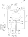
도 1은 내부 방사형 냉각제 유동 경로를 가지는 기판 페데스탈 조립체(116)의 일 실시예를 가지는 전형적인 식각 반응기(100)의 개략적인 도면이다. 여기서 도시된 식각 반응기(100)의 특별한 실시예는 예시적인 목적을 위해 제공되지만 본 발명의 범위를 제한하기 위해 이용되지 않아야 한다.1 is a schematic diagram of a
각각의 반응기(100)는 일반적으로 공정 챔버(110), 가스 패널(138) 및 제어기(140)를 포함한다. 공정 챔버(100)는 공정 용적을 둘러싸는 전도성 바디(벽)(130) 및 천장(120)을 포함한다. 가스 패널(138)로부터의 공정 가스는 샤워헤드 또는 하나 또는 둘 이상의 노즐(136)을 통하여 챔버(110)의 공정 용적으로 제공된다.Each
제어기(140)는 중앙 처리 유닛(CPU)(144), 메모리(142), 및 지지 회로(146)를 포함한다. 제어기(140)는 식각 반응기(100)의 부품에 결합되어 제어하고, 공정이 챔버(110) 내에서 수행될 뿐만 아니라 집적 회로 fab의 데이터베이스와의 기능적 데이터 교환을 용이하게 할 수 있다.The
도시된 실시예에서, 천장(120)은 실질적으로 평면형 유전체 부재이다. 공정 챔버(100)의 다른 실시예들은 다른 타입의 천장, 예를 들면 돔형(dome-shaped) 천장을 가질 수 있다. 천장(120) 위에는 하나 또는 둘 이상의 유도성 코일 요소를 포함하는 안테나(112)가 배치된다(두 개의 공동 축선의 코일 요소들이 예시적으로 도시된다). 안테나(112)는 제 1 정합 네트워크(170)를 통하여, 무선-주파수(RF) 플라즈마 전원(118)으로 결합된다.In the illustrated embodiment, the
일 실시예에서, 기판 페데스탈 조립체(116)는 장착 조립체(162), 베이스 조립체(114) 및 정전 척(188)을 포함한다. 장착 조립체(162)는 베이스 조립체(114)를 공정 챔버(110)으로 결합한다.In one embodiment, the
정전 척(188)은 일반적으로 세라믹 또는 유사 유전체 재료로 형성되고 전원(128)을 이용하여 제어되는 하나 이상의 클램핑 전극(186)을 포함한다. 추가의 일 실시예에서, 정전 척(188)은 제 2 정합 네트워크(124)를 통하여 기판 바이어스의 전원(122)으로 결합되는 하나 이상의 RF 전극(도시안됨)을 포함할 수 있다. 정전 척(188)은 기능적으로 하나 또는 둘 이상의 기판 히터를 포함할 수 있다. 일 실시예에서, 동심 히터(184A, 184B)로서 도시된, 두 개의 동심 및 독립적으로 제어가능한 저항성 히터는 기판(150)의 에지 대 중앙 온도 프로파일을 제어하기 위해 이용된다.The
정전 척(188)은 척의 기판 지지면에 형성되고 열 전달(또는 배면) 가스의 소스(148)로 유체적으로 결합되는, 그루브와 같은, 다수의 가스 통로(도시안됨)를 더 포함할 수 있다. 작동 중, 배면 가스(예를 들면 헬륨(He))는 정전 척(188)과 기판(150) 사이의 열 전달을 강화화도록 제어된 압력으로 가스 통로 내로 제공된다. 종래에는, 정전 척의 기판 지지면에는 기판을 처리하는 동안 이용되는 화학물 및 온도에 내성을 가지는 코팅이 제공된다.The
베이스 조립체(114)는 일반적으로 알루미늄 또는 다른 금속 재료로 형성된다. 베이스 조립체(114)는 가열 또는 냉각 유체의 소스(182)로 결합되는 하나 또는 둘 이상의 냉각 통로를 포함한다. 다른 것 중에서, 프레온, 헬륨 또는 질소와 같은 하나 이상의 가스, 또는 다른 것 중에서 물 또는 오일과 같은 액체일 수 있는 열 전달 유체는 베이스 조립체(114)의 온도를 제어하도록 통로를 통하여 소스(182)에 의해 제공되어, 베이스 조립체(114)를 가열 또는 냉각하여, 처리 동안 베이스 조립체(114) 상에 배치되는 기판(150)의 온도를 부분적으로 제어한다.
페데스탈 조립체(116) 및 이에 따른 기판의 온도는 다수의 센서(도 1에 도시안됨)를 이용하여 모니터링된다. 페데스탈 조립체(116)를 통한 센서들의 루팅(routing)이 추가로 후술된다. 광 섬유 온도 센서와 같은, 온도 센서는 제어기(140)에 결합되어 페데스탈 조립체(116)의 온도 프로파일을 나타내는 계량(metric)을 제공하도록 한다.The temperature of the
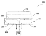
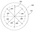
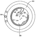
도 2a 내지 도 2b는 기판 페데스탈 조립체(116)의 균일한 온도 제어를 제공하도록 구성되는 냉각 유동 경로(200)를 도시하는 기판 페데스탈 조립체(116)의 일 실시예의 개략적인 단면도 및 평면도이다. 기판 페데스탈 조립체(116)는 베이스 조립체(114) 상에 배치되는 정전 척(188)을 포함한다. 유동 경로(200)는 베이스 조립체(114)를 통하여 형성된 하나 또는 둘 이상의 통로를 통하여 루팅될 수 있다. 유동 경로(200)는 일반적으로 베이스 조립체(114)를 통하여 방사형 배향(radial orientation)을 가진다. 비록 소스(182)에 의해 제공된 열 전달 유체가 방사형 외측으로 유동하도록 중앙 입구를 가지는 도 2a 내에 유동 경로(200)가 도시되지만, 유동의 방향이 반대로 될 수 있다는 것이 고려된다.2A-2B are schematic cross-sectional and top views of one embodiment of a
일 실시예에서, 유동 경로(200)는 제 1 방사형 경로(202) 및 제 2 방사형 경로(204)를 포함한다. 제 1 및 제 2 방사형 경로(202, 204)는 실질적으로 반대 방향으로 열 전달 유체의 유동을 지향시키도록 구성된다. 베이스 조립체(114)는 일반적으로 정전 척(188) 보다 직경이 더 커서, 제 1 및 제 2 방사형 경로(202, 204)가 기판의 에지에서 유용한 온도 제어를 제공하도록 척(188) 및 기판(150)의 외경을 넘어 반지름 방향으로 연장하도록 한다.In one embodiment, the
도 2a 및 도 2b의 도시된 실시예에서, 제 1 방사형 경로(202)는 정전 척(188)과 접촉하는 베이스 조립체(114)의 표면에 인접하며, 반면 제 2 방사형 경로(204)는 제 1 방사형 경로(202) 아래 배치된다. 일 실시예에서, 유동 경로(200)는 버섯 형상을 가지며, 예를 들면 실질적으로 원환체(torus)이다. 토로이달 형상의 유동 경로(200)는 다수의 개별 방사형 통로, 또는 단일 통로로 이루어질 수 있다.In the illustrated embodiment of FIGS. 2A and 2B, the first
토로이달 형상은 종래의 베이스에서 이용되는 유동 경로의 길이를 상당히 감소한다. 예를 들면, 300 mm 기판을 처리하기에 적절한 동등한 크기의 베이스에서, 본 발명의 일 실시예의 유동 경로의 구성은 유동 경로의 길이를 종래의 기판 지지부의 베이스에서의 약 72 인치로부터 약 6 인치로 감소한다. 길이에서의 이러한 감소는 냉각 통로의 입구와 출구 사이의 온도 강하를 감소하여, 기판 지지 페데스탈 내의 온도 구배를 상당히 감소시킨다. 일 실시예에서, 냉각 통로의 입구와 출구 사이의 온도 델타(temperature delta)는 종래의 기판 지지부에서의 약 7 내지 약 17℃에 비해 약 0.1 내지 약 1.0이다. 유체 입구 온도 범위는 (-)30 내지 약 (+)85℃ 사이와 같은, (-) 100℃ 내지 약 (+)200℃일 수 있다. 방사형 유동 경로의 이러한 배치에 의해 또한 유동 저항이 상당히 감소되어 선택된 작동 압력에서 더 큰 유체 유동 및 더 높은 열 전달율을 허용한다.The toroidal shape significantly reduces the length of the flow path used in conventional bases. For example, in an equally sized base suitable for processing a 300 mm substrate, the configuration of the flow path in one embodiment of the present invention may vary the length of the flow path from about 72 inches to about 6 inches at the base of a conventional substrate support. Decreases. This reduction in length reduces the temperature drop between the inlet and the outlet of the cooling passages, significantly reducing the temperature gradient in the substrate support pedestal. In one embodiment, the temperature delta between the inlet and the outlet of the cooling passage is about 0.1 to about 1.0 compared to about 7 to about 17 degrees Celsius in a conventional substrate support. The fluid inlet temperature range can be from (−) 100 ° C. to about (+) 200 ° C., such as between (−) 30 to about (+) 85 ° C. This arrangement of radial flow paths also significantly reduces flow resistance, allowing for greater fluid flow and higher heat transfer rates at selected operating pressures.
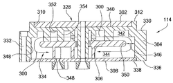
도 3은 도 1의 베이스 조립체(114)의 단면도이다. 일 실시예에서, 베이스 조립체(114)는 배향이 실질적으로 방사형인 내부 냉각제 유동 경로(300)를 포함한다. 또 다른 실시예에서, 유동 경로(300)는 유동 경로(200)를 참조하여 설명된 바와 같이 구성될 수 있다.3 is a cross-sectional view of the
일 실시예에서, 베이스 조립체(114)는 상부 커버 판(302), 베이스 판(304), 채널 분리 판(channel separator plate; 306) 및 바닥 커버 판(308)을 포함한다. 판들(302, 304, 306, 308)은 일반적으로 유용한 열 전도체, 예를 들면, 스테인레스 강 또는 알루미늄과 같은 금속으로 제조될 수 있다.In one embodiment, the
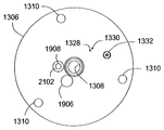
상부 커버 판(302)은 베이스 판(304)의 상부(312)에 형성된 리세스(310)에 배치된다. 리세스(310)의 깊이는 상부 커버 판(302)의 상부면(328)이 베이스 판(304)의 상부(312)와 실질적으로 동일 평면상에 있도록 선택될 수 있다. 정전 척(188)(도 3에 도시 안됨)은 상부 커버 판(302)의 적어도 하나의 상부면(328)을 지지한다.The
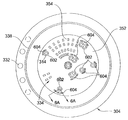
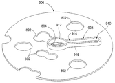
도 4에 도시된 베이스 조립체(114)의 평면도를 부가적으로 참조하면, 상부 커버 판(302)은 다수의 통공을 포함한다. 통공은 리프트 핀 및 베이스 조립체(114)를 통하여 정전 척(188)으로의 다양한 히터, 센서, 가스 및 파워 유틸리티(utility)의 루팅(routing)을 위해 이용된다. 도 4에 도시된 실시예에서, 통공(314)은 리프트 핀을 위해 제공되고, 통공(316)은 척 파워 유틸리티를 위해 제공되고, 통공(318)은 히터 요소를 위해 제공되고, 통공(320)은 온도 센서를 위해 제공되고, 그리고 통공(324, 326)은 상부 커버 판(302)과 정전 척(188) 사이로의 열 전달 가스의 전달을 위해 제공된다. 동일한 도면 부호가 베이스 조립체(114)의 다른 부품의 루팅을 위해 이용되는 베이스 조립체(114)의 다른 부품 내의 통공을 확인하기 위해 이용될 수 있다.Additionally referring to the top view of the
베이스 판(304)은 다수의 장착공(332)이 관통 형성되는 스텝(step; 330)을 포함한다. 명료성을 위해 하나가 도시된, 장착 구멍(332)은 일반적으로 스텝(33) 상의 볼트 원형부(circle) 상에 배치된다. 스텝(330)은 베이스 판(302)의 상부 외측 및 아래 배치되어, 또한 기판(150)의 에지 밖에 있다.The
도 5는 커버 판(302)이 베이스 판(304)의 리세스된 표면(recessed surface; 340)이 노출하도록 제거된 기판 페데스탈(114)의 평면도이다. 리세스된 표면(340)은 그 내부에 형성된 다수의 냉각 채널을 포함한다. 도 5에 도시된 실시예에서, 내부 냉각 채널(502) 및 외부 냉각 채널(504)이 제공된다. 헬륨, 또는 다른 열 전달 가스 또는 유체가 각각의 입구(506, 508)를 통하여 냉각 채널(502, 504)에 제공된다. 열 전달 가스는 채널(502, 504)을 통하여 커버 판(302)(도 4에 도시됨) 내의 다수의 통공(324, 326)으로 분배되며, 다수의 통공을 통하여 열 전달 가스가 정전 척(188)과 베이스 조립체(114) 사이로 분배된다. 채널(502, 504) 내의 유체의 온도는 중앙 대 에지 깊은 온도 제어를 제공하는데 도움이 되도록 독립적으로 조절된 온도를 가질 수 있다.5 is a top view of the
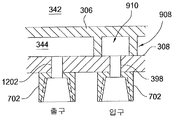
도 3을 다시 참조하면, 베이스 판(304)은 베이스 판(304)의 바닥(336) 내에 형성된 공동(334)을 포함한다. 바닥 커버 판(308)은 공동(334) 내에 채널 분리 판(306)을 밀봉하도록 베이스 판(304)의 바닥(336)에 밀봉가능하게 결합된다. 일 실시예에서, 바닥 커버 판(308)은 베이스 판(304)의 바닥(336)에 형성된 스텝(338)에 배치되어, 연속 용접 또는 다른 적절한 기술에 의해 베이스 판(304)에 대해 밀봉된다.Referring back to FIG. 3, the
채널 분리 판(306)은 공동(334)을 두 개의 디스크형 플레넘(disc-shaped plenum; 342, 344)으로 나눌 수 있다. 플레넘(342, 344)은 수직방향으로 적층되어 공동(344)의 외측 측벽(346)과 채널 분리 판(306)의 외측 에지 사이로 형성되는 갭(346)을 통하여 유체 결합된다. 도 3에 도시된 실시예에서, 방사형 냉각제 유동 경로는 갭(348)을 통하여 하부 플레넘(344) 내로 상부 플레넘(342)을 통하여 형성된다. 유동 경로를 통한 유동의 방향이 반대로 될 수 있다는 것도 고려된다.The
일 실시예에서, 채널 분리 판(306)은 다수의 스페이서(354)에 의해 공동(334)의 상부 벽(352)으로부터 이격된 관계로 유지된다. 스페이서(354)는 베이스 판(304)의 부분이다. 적어도 일부의 스페이서(354)는 상부 플레넘(342)을 통한 유동이 직접 방사형이 되도록 방사형 배향을 가질 수 있다.In one embodiment, the
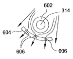
도 6은 상부 벽(352)으로부터 돌출하는 스페이서(354)를 도시하는 베이스 판(304)의 저면도이다. 스페이서(354)가 베이스 판(304)의 중앙선 둘레 360도로 분배될 때 명료성을 위해 단지 적은 개수의 스페이서(354)가 도 6에 도시된다. 적어도 일부의 스페이서(354)는 상부벽(352)과 채널 스페이서 판(306) 사이의 공간을 연결한다. 스페이서(354)의 개수, 배향, 분포 및 크기는 베이스 판(304)으로부터 상부 플레넘(342) 내에 배치된 유체로 원하는 프로파일의 열 전달을 제공하도록 선택될 수 있다. 도 6에 도시된 실시예에서, 스페이서(354)는 길이가 연장되고 방사형 유동 방향과 정렬되는 주요 축선을 가진다. 또한 베이스 판(304)의 중앙선으로부터 동일한 반경에 위치되는 두 개의 인접한 스페이서(354) 사이로 통과하는 유동이 다음 외향 스페이서(354)를 향하여 지향되도록 스페이서(354)를 엇갈리게 배치되어, 냉각 유체가 갭을 향하여 외측으로 이동할 때 냉각 유체의 측방향 운동 및 혼합을 일으키도록 한다.6 is a bottom view of
부가적으로 도 6에 도시된 것은 다양한 통공(314, 316, 318, 320, 322, 324, 326)이 관통 연장하는 다수의 보스(602)이다. 보스(602)는 통공과 플레넘(342) 사이에 배리어를 제공한다. 보스(602)는 페데스탈 조립체(116)를 통하여 유틸리티, 센서, 히터, 유체, 등의 루팅을 용이하게 하도록 베이스 커버 판(308)의 외부에 존재하는 보어(702)(도 7에 도시됨)와 정렬된다. 바닥 커버 판(308)과 베이스 판(304) 사이의 연결은 통공 내로 유체의 유입을 방지하도록 또 다른 적절한 방식으로 브레이징(braze) 또는 밀봉될 수 있다.Additionally shown in FIG. 6 are a number of
도 6a 내지 도 6b의 상세도를 부가적으로 참조하면, 유동 디렉터(604)는 보스의 후방 측부 둘레로 플레넘(342)을 통하여 유동하는 열 전달 유체의 래핑(wrapping)을 증진하도록 보스(604) 각각의 하류측부 상에 제공될 수 있다. 일 실시예에서, 유동 디렉터(604)는 스페이서(354)의 배향에 대해 실질적으로 직각의 배항을 가진다. 유동 디렉터(604)는 부가적으로 보스(602)와 디렉터(604) 사이로 지향된 유체가 도 6b에 도시된 화살표에 의해 도시된 바와 같이, 누출되어 보스(602)와 디렉터(604) 사이의 유동을 유지하도록 하나 또는 둘 이상의 슬롯(606)을 포함할 수 있다. 선택적으로, 유동 디렉터(604)는 베이스 판(304)의 상부 벽(352)과 채널 분리 판(306) 사이의 공간이 연결되지 않을 수 있어, 보스(602)와 디렉터(604) 사이의 유체의 일 부분이 디렉터(604) 위로 누출될 수 있도록 둑(weir)으로서 기능한다. 유체의 래핑은 보스(604)로부터 유용한 열 전달을 증진하여, 통공의 공간을 통하여 낮은 열 전달율을 보상한다.Further referring to the detail view of FIGS. 6A-6B, the
도 8은 채널 분리 판(306)의 일 실시예의 평면도이다. 채널 분리 판(306)은 다수의 구멍(802)을 포함하며 다수의 구멍을 통하여 베이스 판(304)의 보스가 관통 연장한다. 채널 분리 판(306)은 또한 하나 또는 둘 이상의 유입 구멍(804)을 포함하며 이 구멍은 아래 설명되는 바와 같이 공동(334) 내로 냉각제 유체의 유입을 허용한다.8 is a plan view of one embodiment of a
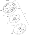
도 9 내지 도 10은 채널 분리 판(306)의 저면도 및 저면 사시도이다. 채널 분리 판(306)은 유입 구멍(806)으로 열 전달 유체를 제공하기 위해 측방향 공급부(908)를 포함한다. 측방향 공급부(908)는 페데스탈 조립체(116)의 열 전달 유체 입구가 페데스탈의 중앙으로부터 오프셋되는 것을 허용하여 전기적 유틸리티, 리프트 핀, 가스 채널 등을 루팅하기 위한 더욱 효율적인 공간 이용을 허용한다. 도 9에 도시된 일 실시예에서, 측방향 공급부(908)는 채널 분리 판(306)의 바닥으로부터 돌출하는 벽(916)에 의해 형성된다. 벽(916)은 측방향 공급부(908)의 제 1 단부에서 외부 플레넘(910), 측방향 공급부(908)의 제 2 단부에서 내부 플레넘(912), 및 플레넘들(910, 912)에 유체 결합하는 채널을 둘러싸는, 일반적으로 중공형-개뼈 형상(hollow dog-bone shape)을 가진다. 외부 플레넘(910)은 일반적으로 채널 분리 판(306)의 중앙으로부터 외측으로 위치된다. 외부 플레넘(910)은 바닥 커버 판(308) 내에 형성된 유체 유입 구멍(398)과 정렬하도록 위치된다(도 3 및 도 12에 도시된 바와 같이). 내부 플레넘(912)은 일반적으로 채널 분리 판(306)의 중앙에 위치된다. 내부 플레넘(912)을 둘러싸는 벽(916)의 부분은 측방향 공급부(908)로부터의 유체가 채널 분리 판(306) 내의 구멍(804)을 통하여 채널 분리 판(306)의 상 측부에 형성된 중앙 분배 플레넘 내로 지향하도록 내부 구멍(804)을 둘러싸기에 충분하게 넓다.9-10 are bottom and bottom perspective views of the
도 11은 중앙 분배 플레넘(1102)의 일 실시예를 도시하는 베이스 조립체(114)의 확대 단면도이다. 중앙 분배 플레넘(1102)은 상부 상의 베이스 판(304) 및 바닥 상의 채널 분리 판(306)에 의해 경계가 형성된다. 벽(11096)은 베이스 판(304)으로부터 하방으로 연장하여 중앙 분배 플레넘(1102)의 외측 경계를 제공한다. 벽(6)은 구멍(804)이 플레넘들(912, 920) 사이에 유체 통로를 제공하는 것을 허용하도록 구멍(804)의 외측에 위치된다. 벽(1106)은 화살표 1104에 의해 도시된 바와 같이, 유체가 중앙 분배 플레넘(1102)으로부터 상부 플레넘(342) 내로 방사형으로 누출되는 것을 허용하도록 구성된다.11 is an enlarged cross sectional view of the
일 실시예에서, 벽(1106)은 구멍 또는 슬롯과 같은, 하나 또는 둘 이상의 통로(1110)를 포함하며, 구멍 또는 슬롯을 통하여 유체가 중앙 분배 플레넘(1102)으로부터 상부 플레넘(342) 내로 누출될 수 있다. 일 실시예에서, 통로(1110)는 관통 구멍이다. 도 11에 도시된 실시예에서, 벽(1106)은 말단부에 형성된 통로(1110)를 가지는, 일반적인 원통형 형상을 가진다. 통로(1110)는 벽(1106)을 따라 균등하게 구분될 수 있다. 선택적으로, 하나 또는 둘 이상의 통로(1110)는 유체의 유동을 모든 반지름 방향으로 동일하게 지향되도록 하는 연속 둑으로서 구성될 수 있다. 선택적으로, 통로(1110)의 개수 및 간격은 원하는 경우 상부 플레넘(342)의 또 다른 영역에 대해 상부 플레넘(342)의 하나의 영역으로 더 많이 유동을 지향하도록 선택될 수 있다.In one embodiment, the
도 11에 도시된 바와 같이, 베이스 판(306)은 플레넘(912, 1102) 내의 유체로부터 중앙 통로(1112)를 고립시키는 중앙 보스(1108)를 포함한다. 중앙 통로(1112)는 상부 커버 판(302)을 통과하여 형성되는 통공(316) 및 바닥 커버 판(308)을 통하여 형성되는 구멍(1118)과 정렬된다. 통로(1112), 통공(316) 및 구멍(1118)은 페데스탈 조립체(116)를 통하여 정전 척(1118)으로 유틸리티의 루팅을 용이하게 한다. 바닥 커버 판(308)과 보스(1108) 사이의 조인트는 통로 내로 유체의 유입을 방지하도록 또 다른 적절한 형태로 밀봉 또는 브레이징될 수 있다. 도 11의 보스(1114)로서 도시된, 바닥 커버 판(308)의 보스(702)들 중 하나는 유틸리티 도관의 커플링을 용이하게 하도록 내부에 형성된 포트(1116)를 가진다. 다른 보스(702)는 유사하게 구성된다.As shown in FIG. 11, the
페데스탈 조립체(116)를 통과하는 유동 경로의 유체 출구가 도 12의 부분 단면도에 도시된다. 유체 출구 구멍(1202)은 하부 플레넘(344)을 배수하도록 바닥 커버 판(308)을 통하여 형성된다. 출구 구멍(1202)은 일반적으로 입구 구멍(398) 근처에 위치된다. 도 12의 입구 보스(1204) 및 출구 보스(1206)로서 도시된, 바닥 커버 판(308) 상에 형성된 보스들(702) 중 두 개의 보스는 구멍(398, 1202)을 통하여 유동 경로(300)로의 유체 연결을 제공하도록 이용된다. 일 실시예에서, 보스(1204)는 열 전달 유체 소스(182)로 결합되고 보스(1206)는 배출부로 결합되거나 유체 소스(182)를 통하여 역으로 재순환된다. 유동 경로(300)를 통하여 제공된 냉각 유체의 열 전달 매체의 압력, 유량, 온도, 밀도 및 구성은 페데스탈 조립체(116)를 통한 열 전달 프로파일의 강화된 제어를 제공한다. 더욱이, 유동 경로(300) 내의 유체의 밀도, 압력 및 유량이 기판(150)의 처리 동안 인-시츄(in-situ) 제어될 수 있을 때, 기판(150)의 온도 제어는 처리 성능을 추가로 강화하도록 처리 동안 변경될 수 있다.The fluid outlet of the flow path through the
작동 중, 기판(150)은 페데스탈 조립체(116) 상에 제공된다. 전력(power)은 기판을 고정하기 위해 정전 척(188)으로 제공된다. 전력은 기판(150)의 측방향 온도 프로파일의 제어를 제공하도록 정전 척(188) 내부의 히터로 제공된다. 액체 및/또는 프레온과 같은 가스일 수 있는 냉각제 유체는 기판의 정밀한 온도 제어를 가능하게 하도록 베이스 조립체(1114) 내에 형성된 방사형 냉각 경로를 통하여 제공된다.In operation, the
일 실시예에서, 냉매는 중앙 분배 플레넘(1102)으로 제공되며, 중앙 분배 플레넘으로부터 냉매가 하나 또는 둘 이상의 통로(1110)를 통하여 디스크형 상부 플레넘(342) 내로 방사형으로 분배된다. 유동 디렉터(604)는 플레넘(342)을 통하여 연장하는 다양한 보스(604) 둘레로 상부 플레넘(342)을 통하여 유동하는 열 전달 유체의 래핑을 증진하기 위해 이용된다. 이어서 냉매는 상부 플레넘(342)으로부터 갭(348)을 통하여 하부 디스크형 플레넘(344) 내로 유동하고, 하부 디스크형 플레넘으로부터 냉매가 긍극적으로 제거된다. 횡단 유동 배향을 따라, 냉매 유동 경로의 방사형 구성은 냉매 경로 길이 및 압력 강하를 감소시켜, 유익하게는 페데스탈 조립체(116)의 강화된 냉각 균일도에 기여하여, 반응기(100) 내의 개선된 공정 제어를 가능하게 한다.In one embodiment, the coolant is provided to the
예를 들면, 상기 언급된 기판 온도 제어는 식각 공정 동안 유익하게 적용될 수 있으며, 여기에서 플라즈마는 가스 패널(138)로부터 제공된 가스로부터 반응기(100) 내에 형성된다. 위에서 언급되고 진공 챔버 내에서 수행되고 및/또는 정밀한 온도 제어를 요구하는 것과 같은, 다른 기판 제조 공정은 또한 여기서 설명된 온도 제어 방법 및 장치의 이용으로부터 유익할 수 있다.For example, the above-mentioned substrate temperature control can be advantageously applied during the etching process, where a plasma is formed in the
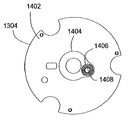
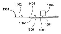
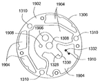
도 13은 베이스 조립체(1300)의 또 다른 실시예의 분해 사시도이며, 베이스 조립체를 통하여 열 전달 유체가 상부 디스크형 플레넘으로부터 하부 디스크형 플레넘 내로 유동하고 하부 디스크형 플레넘으로부터 유체가 긍극적으로 제거된다. 베이스 조립체(1300)는 베이스 판(1302), 채널 분리 판(1304) 및 바닥 커버 판(1306)을 포함한다. 베이스 판(1302) 및 바닥 커버 판(1306)은 서로 밀봉가능하게 결합되어 그 사이에서 채널 분리 판(1306)을 잡아서 채널 분리 판 및 베이스 판 사이로 도입되는 냉매 유체가 채널 분리 판(1304)의 외경(1314) 외측 및 위로 채널 분리 판(1304)과 바닥 커버 판(1306) 사이에 형성된 바닥 플레넘 내로 유동하도록 한다. 베이스 판(1302), 채널 분리 판(1304) 및 바닥 커버 판(1306) 모두 중앙 통공(1308)을 포함하며 중앙 통공은 베이스 판(1302)의 상부(1316)에 결합되는 정전 척(188)(도 1에 도시됨)을 전력 및 다른 유틸리티를 루팅하기 위한 도관을 제공한다.13 is an exploded perspective view of another embodiment of the
베이스 판(1302) 및 바닥 커버 판(1306)은 또한 다수의 리프트 핀 구멍(1310)을 포함한다. 채널 분리 판(1304)은 외경(1314)에 형성된 다수의 노치(1312)를 포함하며, 다수의 노치는 리프트 핀 구멍(1310)과 정렬되어 채널 분리 판(1304)이 리프트 핀의 작동과 간섭되지 않는다.
베이스 판(1302)의 상부(1316)는 부가적으로 내부 채널(1318) 및 외측 냉각 채널(1320)을 포함한다. 내부 채널(1318)은 베이스 판(1302)을 통하여 형성된 입구(1322)를 통하여 공급된다. 외부 채널(1320)은 베이스 판(1302)을 통하여 형성된 입구(1324)를 통하여 공급된다. 냉각 유체 공급부(1328, 1330)는 바닥 커버 판(1306)에 제공되고 입구(1320, 1322)와 정렬되어 헬륨, 질소 또는 다른 유체와 같은 유체가 베이스 조립체를 통하여 냉각 채널(1318, 1322)로 루팅되어 조립체(1300) 및 정전 척(118) 사이의 열 전달을 강화하도록 한다. 통공(1326)은 입구(1322, 1324)로 냉각 공급부(1328, 1330)의 결합을 용이하게 하도록 채널 분리 판(1304) 내에 제공된다.
통로(1332)는 또한 베이스 판(1302), 채널 분리 판(1304) 및 바닥 커버 판(1306)을 통하여 제공되어 열 커플링의 통로를 허용하도록 한다. 바닥 커버 판(1306)은 또한 한 쌍의 통공(1334, 1336)을 포함하여 아래에서 추가로 설명되는 바와 같이 베이스 조립체(1300) 내로 및 외부로의 냉각 유체의 유동을 용이하게 한다.
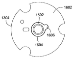
도 14 내지 도 16은 채널 분리 판(1304)의 바닥, 상부 및 측면도이다. 채널 분리 판(1304)은 바닥(1402) 및 상부(1602)를 포함한다. 제 1 보스(1404)는 바닥(1402)로부터 연장하여 리세스가 채널 분리 판(1304)의 상부(1602) 내에 형성된다. 제 1 보스(1404) 내에 형성된 리세스는 채널 분리 판(1304)의 상부(1602)로부터 연장하는 입구 매니폴드 케이지(1502)의 일 부분을 수용한다. 제 2 보스(1406)는 채널 분리 판(1304)의 바닥(1402)으로부터 제 1보스(1404)로부터 연장한다. 제 2 보스(1406)는 채널 분리 판(1304)을 통하여 형성된 통로(1408)를 포함한다. 통로(1408)는 베이스 조립체(1300)로 유입하는 유체가 유입 매니폴트 케이지(1502)를 통하여 그리고 채널 분리 판(1304)과 베이스 판(1302) 사이에 형성된 상부 플레넘 내로 유동하는 것을 허용한다.14-16 are bottom, top, and side views of the
유입 매니폴드 케이지(1502)는 측부(1504) 및 상부(1506)를 포함한다. 다수의 윈도우(1508)는 유입 매니폴드 케이지(1502)의 측부(1504)를 통하여 형성되어 채널 분리 판(1304)과 베이스 판(1302) 사이에 형성된 상부 플레넘을 통로(1408)를 통하여 베이스 조립체(1300)로 유입하는 유체의 유동을 용이하게 하도록 한다. 윈도우(1508)는 구멍, 슬롯 또는 유체가 이를 통하여 유동하도록 하기 위한 다른 피쳐일 수 있다.
유입 매니폴드 케이지(1502)는 중앙 통공(1308)을 둘러싸는 링(1604)을 포함한다. 연장부(1606)는 링(1604)의 외경에 형성되어 제 2 보스(1406)를 통하여 형성된 통로(1408)와 정렬되어 제 2 보스(1406)를 통하여 지향된 유체가 유입 매니폴드 케이지(1502) 내에 형성된 용적 내로 유입되도록 한다.
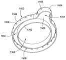
도 17은 유입 매니폴드 케이지(1502)의 일 실시예의 저면 사시도이다. 유입 매니폴드 케이지(1502)는 측부(1504)에 의해 둘러싸이는 고리형 내부 벽(1702)을 포함한다. 유입 매니폴드 케이지(1502)의 내부 벽(1702), 측부(1504) 및 상부(1506)는 매니폴드 케니지(1502) 내에 유체 통로(1704)를 형성한다.17 is a bottom perspective view of one embodiment of
도 18은 채널 분리 판(1304) 및 유입 매니폴드 케이지의 부분 측 단면도이다. 도 18의 실시예에 도시된 바와 같이, 유입 매니폴드 케이지(1502)는 제 1 보스(1404) 내에 형성된 리세스 내에 부분적으로 배치된다. 윈도우(1508)는 상부(1506) 근처의 유입 매니폴드 케이지(1502)의 측부(1504)를 따라 배치되어, 윈도우(1508)가 채널 분리 판(1304)의 상부(1602)로 유체를 제공하도록 위치된다. 따라서, 보스(1406)를 통하여 형성된 통로(1408)를 통하여 유체 통로(1704)로 유입하는 유체는 측부(1504)로부터 외측 반지름 방향으로 상부 플레넘 내로 용이하게 유동할 수 있다.18 is a partial side cross-sectional view of
도 19 내지 도 21은 바닥 커버 판(1306)의 일 실시예의 저면도, 측면도 및 평면도이다. 바닥 커버 판(1306)의 바닥(1902)은 바닥 커버 판(1306)의 열 매스를 감소하도록 바닥 내부에 형성된 다수의 공동(1904)을 포함하여, 조립체(1300)가 더욱 신속하게 가열 및 냉각되는 것을 허용한다. 바닥 커버 판(1306)은 바닥 커버 판을 통하여 형성된 두 개의 구멍(1906, 1908)을 부가적으로 포함하며 두 개의 구멍은 베이스 조립체(1300)로 유입되고 베이스 조립체로부터 배출되는 냉각 유체의 루팅을 용이하게 한다. 구멍(1906)은 채널 분리 판(1304)으로부터 연장하는 보스(1406)를 수용하기에 충분히 크다. 구멍(1906)은 바닥 커버 판(1306)과 채널 분리 판(1304) 사이에 형성된 하부 플레넘의 배출(drain)을 용이하게 한다. 구멍(1908)은 정합 부품과의 정렬을 용이하게 하도록 바닥(1902) 상에 카운터 보어(2158)를 포함할 수 있다.19-21 are bottom, side, and top views of one embodiment of
바닥 커버 판(1306)의 상부(2002)는 제 1 보스(2004) 및 제 2 보스(2006)를 포함한다. 제 1 보스(2004)는 중앙 통공(1308)을 둘러싼다. 제 2 보스(2006)는 온도 감지를 위해 이용되는 제 2 통로를 통과하여 형성된 통로(1332)를 가진다. 바닥 커버 판(1306)은 또한 바닥 커버 판(1306)의 온도를 감지하기 위해 이용되는 온도 탐침을 수용하기 위한 제 2 구멍(1910)을 포함한다.
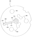
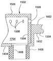
도 22는 페이스 조립체(face assembly; 1300)의 부분 절개 도면이다. 도 22에 도시된 실시예에서, 베이스 판(1302)은 베이스 판(1302)의 바닥 측부로부터 연장하는 립(2250)을 포함한다. 립(2250)은 포켓(2256)의 경계를 형성하는 내측벽(2254)을 가지며 포켓 내에 채널 분리 판(1304) 및 바닥 커버 판(1306)이 수용된다. 바닥 커버 판(1306)의 립(2250)은 예를 들면 연속 용접, 브레이징, 또는 다른 적절한 기술에 의해 베이스 판(1302)에 대해 밀봉되어, 조립체(1300) 내의 상부 및 하부 플레넘을 통해 유동하는 유체를 유지하도록 한다. 포켓(2256)은 채널 분리 판(1304)이 배치되는 바닥(2258)을 가진다. 바닥(2258)은 부가적으로 바닥에 형성된 다수의 채널(2208)을 분리하는 다수의 핀(2206)을 포함한다. 핀(2206) 및 채널(2208)은 도 23 내지 도 26을 참조하여 아래에서 더 상세하게 설명된다. 채널(2208)은 채널 분리 판(1304)과 베이스 판(1302)의 바닥(2258) 사이에 형성된 대부분의 상부 플레넘(2220)을 형성한다. 유체는 입구 매니폴드 케이지(1502) 내에 형성된 윈도우(1508)를 경유하여 상부 플레넘(2220)으로 유입한다. 유체는 입구 매니폴드 케이지(1502)로부터 상부 플레넘(2220)의 채널(2208)을 통하여 그리고 채널 분리 판(1304)의 에지(1314)와 베이스 판(1302)의 내부 벽(2254) 사이에 형성된 거터(2114) 내로 유동한다. 유체는 거터(2114)로부터 바닥 플레넘(2222)으로 그리고 바닥 커버 판(1308)을 통하여 형성된 구멍(1908) 밖으로 유동한다. 따라서, 베이스 조립체(1300)의 플레넘(2220, 2222)을 통한 유동 패턴은 도 2a 내지 도 2b를 참조하여 설명되는 베이스 조립체(114)와 실질적으로 유사하다.FIG. 22 is a partial cutaway view of
바닥 커버 판(1306)은 바닥(2258)으로부터 연장하고 중앙 통공(1308)을 둘러싸는 보스(2260) 및 내부 벽(2254) 내에 형성된 한 쌍의 스텝(2252, 2262) 상에 배치된다. 스텝(2252, 2262)은 패널 분리기 판(1304) 및 바닥 커버 판(1306)을 이격 관계로 유지하여, 하부 플레넘(2222)을 통하여 유동하는 유체에 대한 넓은 공간을 제공한다.The
도 23 내지 도 26은 베이스 조립체(1300)의 바닥판(1302)의 선택적인 저면도이다. 도 23 내지 도 26의 실시예에 공통하는 것은 채널(2208)의 실질적인 방사형 배향 및 플레넘(2220, 2222)을 통한 유동의 마주하는 방사형 방향이다.23-26 are optional bottom views of the
다수의 패드(2210)는 베이스 판(1302)의 바닥면으로부터 연장한다. 일 실시예에서, 7개의 패드가 핀(2206) 위로 연장하는 것이 도시된다. 패드(2210)는 베이스 판(1302)으로부터 채널 분리 판(1304)을 이격시켜, 채널 분리 판(1304)과 핀(2206) 사이에 소형 갭을 형성하여 최소 열 전달이 베이스 판(1302)과 채널 분리 판(1304) 사이로 직접 전달되도록 한다.
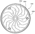
도 23에 도시된 실시예에서, 채널(2208)은 베이스 판(1302)의 바닥에서 외측으로 가로질러 방사형 길이를 따라 실질적으로 균일한 폭 및/또는 단면적을 가진다. 실질적으로 균일한 채널 폭을 수용하도록, 핀(2206)은 플레어형상을 가져서 핀이 베이스 판(1302)의 외측 에지 근처에 있을 때 폭이 더 넓게 된다. 채널(2208)은 선형, 곡선형, 방사 곡선형이거나 또 다른 배향을 가질 수 있다. 도 23에 도시된 실시예에서, 채널(2208)은 곡선형이어서 채널(2208)을 통하여 유동하는 유체가 상부 플레넘(2220) 내에 더 긴 잔류 시간을 가져서, 열 전달 효율을 증가시킨다.In the embodiment shown in FIG. 23, the
도 24에 도시된 실시예에서, 채널(2208)은 메인 채널(2402) 및 메인 채널로부터 분기되는 다수의 서브-채널(sub-channel; 2404)을 포함한다. 도 24에 도시된 실시예에서, 두 개 이상의 서브-채널이 도시된다. 그러나, 메인 채널(2402)은 3개의 서브-채널(2404)을 초과하여 가질 수 있으며, 서브-채널은 자체적으로 두 개 또는 세 개 이상의 보조 채널(도시안됨)로 분기될 수 있다. 서브-채널은 내부 채널 핀(2406)에 의해 분리된다.In the embodiment shown in FIG. 24,
도 25에 도시된 실시예에서, 다수의 채널(2502)은 다수의 라인(2504)에 의해 분리되어 도시된다. 채널(2502)은 채널(2502)이 반지름 외측 방향으로 연장할 때 균일한 단면적 및/또는 폭을 가질 수 있다. 선택적으로, 채널(2502)이 베이스 판(1302)의 외경 근처에 있을 때 채널(2502)의 단면적 및/또는 폭은 플레어형일 수 있다. 도 25에 도시된 실시예에서, 채널(2502)을 분리하는 핀(2504)은 각각의 핀 단부에서 대립하는 것으로서 핀(2504)의 중앙에서 더 두꺼운 실질적으로 부메랑 형상부(boomerang shape)를 가질 수 있다. 부메랑 형상부는 깊게 만곡된 채널(2502)에 대해 허용되어 상부 플레넘(2220)에서 유체의 잔류 시간을 실질적으로 증가시킨다.In the embodiment shown in FIG. 25,
도 26에 도시된 실시예에서, 다수의 채널(2602)은 다수의 핀(2604)에 의해 분리되는 것으로 도시된다. 각각의 핀(2604)은 핀(2604)이 반지름 방향 외측으로 연장할 때, 단면적 및/또는 폭이 실질적으로 균일하다. 대응적으로, 채널이 베이스 판(1302)의 에지를 향하여 외측으로 이동할 때, 채널(2602)은 플레어형이다. 핀(2604)은 반지름 방향으로 선형으로 연장할 수 있거나 핀은 상부 플레넘(2220)을 형성하는 채널(2602) 내의 냉각 유체의 잔류 시간을 증가시키도록 만곡될 수 있다.In the embodiment shown in FIG. 26,
따라서, 방사형 냉매 유동 경로를 포함하는 페데스탈 조립체가 제공된다. 폐데스탈 조립체를 통과하는 방사형 냉매 유동 경로는 개선된 온도 제어를 제공하고, 이에 의해, 기판의 온도 프로파일이 제어되는 것을 가능하게 한다.Thus, a pedestal assembly is provided that includes a radial refrigerant flow path. The radial refrigerant flow path through the closed decentral assembly provides improved temperature control, thereby allowing the temperature profile of the substrate to be controlled.
전술된 것은 본 발명의 실시예에 관한 것이지만, 본 발명의 다른 및 추가의 실시예가 본 발명의 기본적 범위로부터 이탈하지 않고 발명될 수 있으며, 본 발명의 범위는 후술되는 청구범위에 의해 결정된다.While the foregoing is directed to embodiments of the invention, other and further embodiments of the invention may be devised without departing from the basic scope thereof, and the scope thereof is determined by the claims that follow.
Claims (15)
진공 처리 챔버의 기판 페데스탈 조립체 상에 기판을 배치하는 단계,
상기 기판 페데스탈 조립체 내의 방사형 유동 경로를 통하여 열 전달 유체를 유동시킴으로써 상기 기판 페데스탈 조립체의 온도를 제어하는 단계로서, 상기 방사형 유동 경로는 반지름방향 내측부 및 반지름방향 외측부 둘다를 포함하는, 기판 페데스탈 조립체의 온도를 제어하는 단계, 및
온도 제어된 상기 기판 페데스탈 조립체 상의 상기 기판을 플라즈마 처리하는 단계를 포함하는,
처리 동안 기판 온도를 제어하기 위한 방법.
A method for controlling substrate temperature during processing,
Placing the substrate on the substrate pedestal assembly of the vacuum processing chamber,
Controlling the temperature of the substrate pedestal assembly by flowing a heat transfer fluid through the radial flow path in the substrate pedestal assembly, wherein the radial flow path includes both a radially inner portion and a radially outer portion. Controlling it, and
Plasma processing the substrate on the temperature controlled substrate pedestal assembly,
Method for controlling substrate temperature during processing.
상기 기판 플라즈마 처리 단계는 플라즈마 처리, 화학적 증착 공정, 물리적 증착 공정, 이온 주입 공정 또는 식각 공정 중 하나 이상인,
처리 동안 기판 온도를 제어하기 위한 방법.
The method of claim 1,
The substrate plasma treatment step may be at least one of a plasma treatment, a chemical deposition process, a physical deposition process, an ion implantation process, or an etching process.
Method for controlling substrate temperature during processing.
상기 기판 페데스탈 조립체의 온도를 제어하는 단계는:
실질적인 토로이달(toroidal) 유동 경로를 통하여 상기 열 전달 유체를 유동시키는 단계를 포함하는,
처리 동안 기판 온도를 제어하기 위한 방법.
The method of claim 1,
Controlling the temperature of the substrate pedestal assembly includes:
Flowing the heat transfer fluid through a substantially toroidal flow path,
Method for controlling substrate temperature during processing.
상기 유동 경로 내의 장애물 뒤로 상기 열 전달 유체의 유동을 지향시키는 단계를 포함하는,
처리 동안 기판 온도를 제어하기 위한 방법.
The method of claim 1,
Directing the flow of the heat transfer fluid behind an obstacle in the flow path,
Method for controlling substrate temperature during processing.
상기 기판 페데스탈 조립체의 온도를 제어하는 단계는:
상기 열 전달 유체를 상기 기판 페데스탈 조립체의 중앙에 배치되는 플레넘 내로 유동시키는 단계: 및
상기 열 전달 유체를 상기 플레넘으로부터 실질적인 디스크형 플레넘 내로 반지름 방향 외측으로 유동시키는 단계를 포함하는,
처리 동안 기판 온도를 제어하기 위한 방법.
The method of claim 1,
Controlling the temperature of the substrate pedestal assembly includes:
Flowing the heat transfer fluid into a plenum disposed centrally of the substrate pedestal assembly: and
Radially outflowing the heat transfer fluid from the plenum into a substantially disc-shaped plenum;
Method for controlling substrate temperature during processing.
상기 유동시키는 단계는:
상기 열 전달 유체를 제 1 플레넘의 반지름 방향 외측으로 형성된 고리형 갭을 통하여 제 2의 실질적인 디스크형 플레넘 내로 유동시키는 단계를 더 포함하는,
처리 동안 기판 온도를 제어하기 위한 방법.
The method of claim 5, wherein
The flowing step is:
Flowing the heat transfer fluid into a second substantially disc-shaped plenum through an annular gap formed radially outward of the first plenum;
Method for controlling substrate temperature during processing.
정전 척, 및
상기 정전 척이 상부에 고정되는 베이스 조립체를 포함하며,
상기 베이스 조립체는 상기 베이스 조립체 내부에 형성된 냉각 유동 경로를 가지며, 상기 냉각 유동 경로는 반지름 방향 외측으로 유동이 지향되도록 구성되는,
페데스탈 조립체.
Pedestal assembly,
Electrostatic chuck, and
A base assembly to which the electrostatic chuck is fixed thereon;
The base assembly has a cooling flow path formed inside the base assembly, the cooling flow path being configured to direct flow outward in a radial direction,
Pedestal assembly.
상기 베이스 조립체는:
상기 정전 척이 고정되는 베이스 판, 및
상기 베이스 판의 바닥에 밀봉되게 결합되는 바닥 커버 판을 포함하며,
상기 냉각 유동 경로가 상기 베이스 판과 상기 바닥 커버 판 사이에 형성되고 하나 이상의 디스크형 플레넘을 포함하는,
페데스탈 조립체.
The method of claim 7, wherein
The base assembly is:
A base plate to which the electrostatic chuck is fixed, and
A bottom cover plate that is sealingly coupled to the bottom of the base plate,
The cooling flow path is formed between the base plate and the bottom cover plate and includes one or more disc-shaped plenums;
Pedestal assembly.
상기 베이스 조립체는:
상기 정전 척이 고정되는 베이스 판,
상기 베이스 판의 바닥에 밀봉가능하게 결합되는 바닥 커버 판,
상기 베이스 판과 상기 바닥 커버 판 사이에 배치되는 채널 분리 판을 포함하며,
상기 냉각 유동 경로는 상기 채널 분리 판과 상기 베이스 판 사이에 적어도 부분적으로 형성되고 상기 채널 분리 판과 상기 바닥 커버 판 사이에 적어도 부분적으로 형성되는,
페데스탈 조립체.
The method of claim 7, wherein
The base assembly is:
A base plate to which the electrostatic chuck is fixed,
A bottom cover plate sealingly coupled to the bottom of the base plate,
A channel separation plate disposed between the base plate and the bottom cover plate,
The cooling flow path is at least partially formed between the channel separator plate and the base plate and at least partially formed between the channel separator plate and the bottom cover plate,
Pedestal assembly.
상기 베이스 판은:
상기 유동 경로 내로 연장하고 실질적인 반지름 방향 배향을 가지는 다수의 핀을 포함하며, 상기 핀들 중 하나 이상이 선형 배향을 가지거나 곡선형인,
페데스탈 조립체.
The method of claim 9,
The base plate is:
A plurality of fins extending into the flow path and having a substantially radial orientation, wherein at least one of the fins has a linear orientation or is curved,
Pedestal assembly.
상기 다수의 핀들 중 두 개의 핀들 사이에 형성된 하나 이상의 채널이 두 개 이상의 서브-채널로 분기되는,
페데스탈 조립체.
The method of claim 10,
One or more channels formed between two of the plurality of pins branched into two or more sub-channels,
Pedestal assembly.
상기 정전 척이 상부면에 고정되는 베이스 조립체, 및
상기 베이스 조립체 내에 형성된 실질적인 토로이달 유동 경로로서, 상기 베이스 조립체의 바닥면에 형성된 입구 및 출구를 가지는, 토로이달 유동 경로를 포함하는,
페데스탈 조립체.
Electrostatic chuck,
A base assembly to which the electrostatic chuck is fixed to an upper surface;
A substantially toroidal flow path formed in the base assembly, the toroidal flow path having an inlet and an outlet formed in the bottom surface of the base assembly;
Pedestal assembly.
상기 베이스 조립체는:
상기 정전 척이 고정되는 베이스 판,
다수의 패드에 의해 상기 베이스 판에 대해 공간 이격 관계로 배치되는 채널 분리 판으로서, 상기 실질적인 토로이달 유동 경로가 상기 채널 분리 판의 외측 에지 위로 연장하는, 채널 분리 판,
상기 채널 분리 판에 대해 공간 이격 관계로 상기 베이스 판의 바닥에 밀봉되게 결합되는 바닥 커버 판을 포함하는,
페데스탈 조립체.
The method of claim 12,
The base assembly is:
A base plate to which the electrostatic chuck is fixed,
A channel separator plate disposed in a spaced apart relationship relative to the base plate by a plurality of pads, wherein the substantially toroidal flow path extends over an outer edge of the channel separator plate,
A bottom cover plate sealingly coupled to the bottom of the base plate in a spaced apart relationship relative to the channel separating plate;
Pedestal assembly.
상기 바닥 커버 판은:
상기 바닥 커버 판과 상기 채널 분리 판 사이로 형성된 공간으로 개방되는 제 1 구멍, 및
상기 베이스 판과 상기 채널 분리 판 사이로 형성된 공간으로 유체적으로 결합되는 제 2 구멍을 포함하는,
페데스탈 조립체.
The method of claim 13,
The bottom cover plate is:
A first hole opening into a space formed between the bottom cover plate and the channel separating plate, and
A second hole fluidly coupled to a space formed between the base plate and the channel separation plate,
Pedestal assembly.
상기 베이스 판은:
상기 유동 경로 내로 연장하는 다수의 곡선형 핀을 포함하는,
페데스탈 조립체.The method of claim 13,
The base plate is:
A plurality of curved pins extending into the flow path,
Pedestal assembly.
Applications Claiming Priority (2)
| Application Number | Priority Date | Filing Date | Title |
|---|---|---|---|
| US1600007P | 2007-12-21 | 2007-12-21 | |
| US61/016,000 | 2007-12-21 |
Publications (1)
| Publication Number | Publication Date |
|---|---|
| KR20100103627A true KR20100103627A (en) | 2010-09-27 |
Family
ID=40787366
Family Applications (1)
| Application Number | Title | Priority Date | Filing Date |
|---|---|---|---|
| KR1020107016261A KR20100103627A (en) | 2007-12-21 | 2008-12-18 | Method and apparatus for controlling temperature of a substrate |
Country Status (6)
| Country | Link |
|---|---|
| US (1) | US20090159566A1 (en) |
| JP (1) | JP2011508436A (en) |
| KR (1) | KR20100103627A (en) |
| CN (1) | CN101903996B (en) |
| TW (1) | TW200937563A (en) |
| WO (1) | WO2009086013A2 (en) |
Cited By (1)
| Publication number | Priority date | Publication date | Assignee | Title |
|---|---|---|---|---|
| KR20180009090A (en) * | 2016-07-18 | 2018-01-26 | 세메스 주식회사 | Chuck of supporting substrate and probe station having the same |
Families Citing this family (120)
| Publication number | Priority date | Publication date | Assignee | Title |
|---|---|---|---|---|
| US20060105182A1 (en) * | 2004-11-16 | 2006-05-18 | Applied Materials, Inc. | Erosion resistant textured chamber surface |
| US7221553B2 (en) * | 2003-04-22 | 2007-05-22 | Applied Materials, Inc. | Substrate support having heat transfer system |
| WO2011056433A2 (en) * | 2009-11-03 | 2011-05-12 | Applied Materials, Inc. | Temperature control of a substrate during a plasma ion implantation process for patterned disc media applications |
| JP2011184738A (en) * | 2010-03-09 | 2011-09-22 | Fujifilm Corp | Method for producing gas barrier film |
| US8772103B2 (en) * | 2010-10-25 | 2014-07-08 | Texas Instruments Incorporated | Low temperature implant scheme to improve BJT current gain |
| US9719169B2 (en) * | 2010-12-20 | 2017-08-01 | Novellus Systems, Inc. | System and apparatus for flowable deposition in semiconductor fabrication |
| US10283321B2 (en) | 2011-01-18 | 2019-05-07 | Applied Materials, Inc. | Semiconductor processing system and methods using capacitively coupled plasma |
| US9245717B2 (en) | 2011-05-31 | 2016-01-26 | Lam Research Corporation | Gas distribution system for ceramic showerhead of plasma etch reactor |
| US8562785B2 (en) * | 2011-05-31 | 2013-10-22 | Lam Research Corporation | Gas distribution showerhead for inductively coupled plasma etch reactor |
| US9196513B2 (en) * | 2011-08-30 | 2015-11-24 | Watlow Electric Manufacturing Company | System and method for controlling a thermal array |
| US20130276980A1 (en) * | 2012-04-23 | 2013-10-24 | Dmitry Lubomirsky | Esc with cooling base |
| US10537013B2 (en) * | 2012-04-23 | 2020-01-14 | Applied Materials, Inc. | Distributed electro-static chuck cooling |
| US9267739B2 (en) * | 2012-07-18 | 2016-02-23 | Applied Materials, Inc. | Pedestal with multi-zone temperature control and multiple purge capabilities |
| US9373517B2 (en) | 2012-08-02 | 2016-06-21 | Applied Materials, Inc. | Semiconductor processing with DC assisted RF power for improved control |
| US9132436B2 (en) | 2012-09-21 | 2015-09-15 | Applied Materials, Inc. | Chemical control features in wafer process equipment |
| WO2014116392A1 (en) * | 2013-01-25 | 2014-07-31 | Applied Materials, Inc. | Electrostatic chuck with concentric cooling base |
| US10256079B2 (en) | 2013-02-08 | 2019-04-09 | Applied Materials, Inc. | Semiconductor processing systems having multiple plasma configurations |
| US9362130B2 (en) | 2013-03-01 | 2016-06-07 | Applied Materials, Inc. | Enhanced etching processes using remote plasma sources |
| US9847222B2 (en) | 2013-10-25 | 2017-12-19 | Lam Research Corporation | Treatment for flowable dielectric deposition on substrate surfaces |
| US10217615B2 (en) | 2013-12-16 | 2019-02-26 | Lam Research Corporation | Plasma processing apparatus and component thereof including an optical fiber for determining a temperature thereof |
| US9847240B2 (en) | 2014-02-12 | 2017-12-19 | Axcelis Technologies, Inc. | Constant mass flow multi-level coolant path electrostatic chuck |
| US9309598B2 (en) | 2014-05-28 | 2016-04-12 | Applied Materials, Inc. | Oxide and metal removal |
| US10249511B2 (en) * | 2014-06-27 | 2019-04-02 | Lam Research Corporation | Ceramic showerhead including central gas injector for tunable convective-diffusive gas flow in semiconductor substrate processing apparatus |
| KR102163083B1 (en) * | 2014-07-02 | 2020-10-07 | 어플라이드 머티어리얼스, 인코포레이티드 | Temperature control apparatus including groove-routed optical fiber heating, substrate temperature control systems, electronic device processing systems, and processing methods |
| KR101545119B1 (en) * | 2014-08-14 | 2015-08-18 | (주)얼라이드 테크 파인더즈 | Plasma device |
| US10049921B2 (en) | 2014-08-20 | 2018-08-14 | Lam Research Corporation | Method for selectively sealing ultra low-k porous dielectric layer using flowable dielectric film formed from vapor phase dielectric precursor |
| US9753463B2 (en) * | 2014-09-12 | 2017-09-05 | Applied Materials, Inc. | Increasing the gas efficiency for an electrostatic chuck |
| US9355922B2 (en) | 2014-10-14 | 2016-05-31 | Applied Materials, Inc. | Systems and methods for internal surface conditioning in plasma processing equipment |
| US9966240B2 (en) | 2014-10-14 | 2018-05-08 | Applied Materials, Inc. | Systems and methods for internal surface conditioning assessment in plasma processing equipment |
| US11637002B2 (en) | 2014-11-26 | 2023-04-25 | Applied Materials, Inc. | Methods and systems to enhance process uniformity |
| US10573496B2 (en) | 2014-12-09 | 2020-02-25 | Applied Materials, Inc. | Direct outlet toroidal plasma source |
| US10224210B2 (en) | 2014-12-09 | 2019-03-05 | Applied Materials, Inc. | Plasma processing system with direct outlet toroidal plasma source |
| US11257693B2 (en) | 2015-01-09 | 2022-02-22 | Applied Materials, Inc. | Methods and systems to improve pedestal temperature control |
| US20160225652A1 (en) | 2015-02-03 | 2016-08-04 | Applied Materials, Inc. | Low temperature chuck for plasma processing systems |
| US9728437B2 (en) | 2015-02-03 | 2017-08-08 | Applied Materials, Inc. | High temperature chuck for plasma processing systems |
| US10497606B2 (en) * | 2015-02-09 | 2019-12-03 | Applied Materials, Inc. | Dual-zone heater for plasma processing |
| US9741593B2 (en) | 2015-08-06 | 2017-08-22 | Applied Materials, Inc. | Thermal management systems and methods for wafer processing systems |
| US9691645B2 (en) | 2015-08-06 | 2017-06-27 | Applied Materials, Inc. | Bolted wafer chuck thermal management systems and methods for wafer processing systems |
| US9349605B1 (en) | 2015-08-07 | 2016-05-24 | Applied Materials, Inc. | Oxide etch selectivity systems and methods |
| US10504700B2 (en) | 2015-08-27 | 2019-12-10 | Applied Materials, Inc. | Plasma etching systems and methods with secondary plasma injection |
| US10586718B2 (en) * | 2015-11-11 | 2020-03-10 | Applied Materials, Inc. | Cooling base with spiral channels for ESC |
| US10388546B2 (en) | 2015-11-16 | 2019-08-20 | Lam Research Corporation | Apparatus for UV flowable dielectric |
| US9916977B2 (en) | 2015-11-16 | 2018-03-13 | Lam Research Corporation | Low k dielectric deposition via UV driven photopolymerization |
| JP6530701B2 (en) * | 2015-12-01 | 2019-06-12 | 日本特殊陶業株式会社 | Electrostatic chuck |
| US10780447B2 (en) * | 2016-04-26 | 2020-09-22 | Applied Materials, Inc. | Apparatus for controlling temperature uniformity of a showerhead |
| US10504754B2 (en) | 2016-05-19 | 2019-12-10 | Applied Materials, Inc. | Systems and methods for improved semiconductor etching and component protection |
| US10522371B2 (en) | 2016-05-19 | 2019-12-31 | Applied Materials, Inc. | Systems and methods for improved semiconductor etching and component protection |
| KR102303971B1 (en) * | 2016-07-19 | 2021-09-24 | 엔지케이 인슐레이터 엘티디 | electrostatic chuck heater |
| US10629473B2 (en) | 2016-09-09 | 2020-04-21 | Applied Materials, Inc. | Footing removal for nitride spacer |
| US10062575B2 (en) | 2016-09-09 | 2018-08-28 | Applied Materials, Inc. | Poly directional etch by oxidation |
| US10546729B2 (en) | 2016-10-04 | 2020-01-28 | Applied Materials, Inc. | Dual-channel showerhead with improved profile |
| US9934942B1 (en) | 2016-10-04 | 2018-04-03 | Applied Materials, Inc. | Chamber with flow-through source |
| US10062585B2 (en) | 2016-10-04 | 2018-08-28 | Applied Materials, Inc. | Oxygen compatible plasma source |
| US10062579B2 (en) | 2016-10-07 | 2018-08-28 | Applied Materials, Inc. | Selective SiN lateral recess |
| US9947549B1 (en) | 2016-10-10 | 2018-04-17 | Applied Materials, Inc. | Cobalt-containing material removal |
| US9768034B1 (en) | 2016-11-11 | 2017-09-19 | Applied Materials, Inc. | Removal methods for high aspect ratio structures |
| US10163696B2 (en) | 2016-11-11 | 2018-12-25 | Applied Materials, Inc. | Selective cobalt removal for bottom up gapfill |
| US10242908B2 (en) | 2016-11-14 | 2019-03-26 | Applied Materials, Inc. | Airgap formation with damage-free copper |
| US10026621B2 (en) | 2016-11-14 | 2018-07-17 | Applied Materials, Inc. | SiN spacer profile patterning |
| KR101750409B1 (en) * | 2016-11-17 | 2017-06-23 | (주)디이에스 | Cooling chuck of a semiconductor wafer |
| US10566206B2 (en) | 2016-12-27 | 2020-02-18 | Applied Materials, Inc. | Systems and methods for anisotropic material breakthrough |
| US10431429B2 (en) | 2017-02-03 | 2019-10-01 | Applied Materials, Inc. | Systems and methods for radial and azimuthal control of plasma uniformity |
| US10403507B2 (en) | 2017-02-03 | 2019-09-03 | Applied Materials, Inc. | Shaped etch profile with oxidation |
| US10043684B1 (en) | 2017-02-06 | 2018-08-07 | Applied Materials, Inc. | Self-limiting atomic thermal etching systems and methods |
| US10319739B2 (en) | 2017-02-08 | 2019-06-11 | Applied Materials, Inc. | Accommodating imperfectly aligned memory holes |
| US10559451B2 (en) * | 2017-02-15 | 2020-02-11 | Applied Materials, Inc. | Apparatus with concentric pumping for multiple pressure regimes |
| US10943834B2 (en) | 2017-03-13 | 2021-03-09 | Applied Materials, Inc. | Replacement contact process |
| US10319649B2 (en) | 2017-04-11 | 2019-06-11 | Applied Materials, Inc. | Optical emission spectroscopy (OES) for remote plasma monitoring |
| US11011355B2 (en) * | 2017-05-12 | 2021-05-18 | Lam Research Corporation | Temperature-tuned substrate support for substrate processing systems |
| US11276559B2 (en) | 2017-05-17 | 2022-03-15 | Applied Materials, Inc. | Semiconductor processing chamber for multiple precursor flow |
| US11276590B2 (en) | 2017-05-17 | 2022-03-15 | Applied Materials, Inc. | Multi-zone semiconductor substrate supports |
| US10497579B2 (en) | 2017-05-31 | 2019-12-03 | Applied Materials, Inc. | Water-free etching methods |
| US10049891B1 (en) | 2017-05-31 | 2018-08-14 | Applied Materials, Inc. | Selective in situ cobalt residue removal |
| US10920320B2 (en) | 2017-06-16 | 2021-02-16 | Applied Materials, Inc. | Plasma health determination in semiconductor substrate processing reactors |
| US10541246B2 (en) | 2017-06-26 | 2020-01-21 | Applied Materials, Inc. | 3D flash memory cells which discourage cross-cell electrical tunneling |
| US10727080B2 (en) | 2017-07-07 | 2020-07-28 | Applied Materials, Inc. | Tantalum-containing material removal |
| US10541184B2 (en) | 2017-07-11 | 2020-01-21 | Applied Materials, Inc. | Optical emission spectroscopic techniques for monitoring etching |
| US10354889B2 (en) | 2017-07-17 | 2019-07-16 | Applied Materials, Inc. | Non-halogen etching of silicon-containing materials |
| US10170336B1 (en) | 2017-08-04 | 2019-01-01 | Applied Materials, Inc. | Methods for anisotropic control of selective silicon removal |
| US10043674B1 (en) | 2017-08-04 | 2018-08-07 | Applied Materials, Inc. | Germanium etching systems and methods |
| US10297458B2 (en) | 2017-08-07 | 2019-05-21 | Applied Materials, Inc. | Process window widening using coated parts in plasma etch processes |
| US10128086B1 (en) | 2017-10-24 | 2018-11-13 | Applied Materials, Inc. | Silicon pretreatment for nitride removal |
| US10424487B2 (en) | 2017-10-24 | 2019-09-24 | Applied Materials, Inc. | Atomic layer etching processes |
| US10283324B1 (en) | 2017-10-24 | 2019-05-07 | Applied Materials, Inc. | Oxygen treatment for nitride etching |
| US11236422B2 (en) * | 2017-11-17 | 2022-02-01 | Lam Research Corporation | Multi zone substrate support for ALD film property correction and tunability |
| US10256112B1 (en) | 2017-12-08 | 2019-04-09 | Applied Materials, Inc. | Selective tungsten removal |
| US10903054B2 (en) | 2017-12-19 | 2021-01-26 | Applied Materials, Inc. | Multi-zone gas distribution systems and methods |
| US11328909B2 (en) | 2017-12-22 | 2022-05-10 | Applied Materials, Inc. | Chamber conditioning and removal processes |
| US10854426B2 (en) | 2018-01-08 | 2020-12-01 | Applied Materials, Inc. | Metal recess for semiconductor structures |
| US10964512B2 (en) | 2018-02-15 | 2021-03-30 | Applied Materials, Inc. | Semiconductor processing chamber multistage mixing apparatus and methods |
| US10679870B2 (en) | 2018-02-15 | 2020-06-09 | Applied Materials, Inc. | Semiconductor processing chamber multistage mixing apparatus |
| TWI716818B (en) | 2018-02-28 | 2021-01-21 | 美商應用材料股份有限公司 | Systems and methods to form airgaps |
| US10593560B2 (en) | 2018-03-01 | 2020-03-17 | Applied Materials, Inc. | Magnetic induction plasma source for semiconductor processes and equipment |
| US10319600B1 (en) | 2018-03-12 | 2019-06-11 | Applied Materials, Inc. | Thermal silicon etch |
| US10497573B2 (en) | 2018-03-13 | 2019-12-03 | Applied Materials, Inc. | Selective atomic layer etching of semiconductor materials |
| US10573527B2 (en) | 2018-04-06 | 2020-02-25 | Applied Materials, Inc. | Gas-phase selective etching systems and methods |
| US10490406B2 (en) | 2018-04-10 | 2019-11-26 | Appled Materials, Inc. | Systems and methods for material breakthrough |
| US10699879B2 (en) | 2018-04-17 | 2020-06-30 | Applied Materials, Inc. | Two piece electrode assembly with gap for plasma control |
| US10886137B2 (en) | 2018-04-30 | 2021-01-05 | Applied Materials, Inc. | Selective nitride removal |
| JP2019201086A (en) * | 2018-05-15 | 2019-11-21 | 東京エレクトロン株式会社 | Processing device, component, and temperature control method |
| US11908715B2 (en) | 2018-07-05 | 2024-02-20 | Lam Research Corporation | Dynamic temperature control of substrate support in substrate processing system |
| US10755941B2 (en) | 2018-07-06 | 2020-08-25 | Applied Materials, Inc. | Self-limiting selective etching systems and methods |
| US10872778B2 (en) | 2018-07-06 | 2020-12-22 | Applied Materials, Inc. | Systems and methods utilizing solid-phase etchants |
| US10672642B2 (en) | 2018-07-24 | 2020-06-02 | Applied Materials, Inc. | Systems and methods for pedestal configuration |
| US10892198B2 (en) | 2018-09-14 | 2021-01-12 | Applied Materials, Inc. | Systems and methods for improved performance in semiconductor processing |
| US11049755B2 (en) | 2018-09-14 | 2021-06-29 | Applied Materials, Inc. | Semiconductor substrate supports with embedded RF shield |
| US11062887B2 (en) | 2018-09-17 | 2021-07-13 | Applied Materials, Inc. | High temperature RF heater pedestals |
| US11417534B2 (en) | 2018-09-21 | 2022-08-16 | Applied Materials, Inc. | Selective material removal |
| US11217433B2 (en) * | 2018-10-05 | 2022-01-04 | Applied Materials, Inc. | Rotary union with mechanical seal assembly |
| US11682560B2 (en) | 2018-10-11 | 2023-06-20 | Applied Materials, Inc. | Systems and methods for hafnium-containing film removal |
| US11121002B2 (en) | 2018-10-24 | 2021-09-14 | Applied Materials, Inc. | Systems and methods for etching metals and metal derivatives |
| CN111211029B (en) * | 2018-11-21 | 2023-09-01 | 中微半导体设备(上海)股份有限公司 | Multi-zone temperature-control plasma reactor |
| US11437242B2 (en) | 2018-11-27 | 2022-09-06 | Applied Materials, Inc. | Selective removal of silicon-containing materials |
| CN113166941A (en) * | 2018-11-28 | 2021-07-23 | 朗姆研究公司 | Susceptor including vapor chamber for substrate processing system |
| US11721527B2 (en) | 2019-01-07 | 2023-08-08 | Applied Materials, Inc. | Processing chamber mixing systems |
| US10920319B2 (en) | 2019-01-11 | 2021-02-16 | Applied Materials, Inc. | Ceramic showerheads with conductive electrodes |
| JP7288834B2 (en) * | 2019-10-07 | 2023-06-08 | キヤノントッキ株式会社 | Film forming apparatus, film forming method, and electronic device manufacturing method |
| CN112593199B (en) * | 2020-11-25 | 2022-10-21 | 北京北方华创微电子装备有限公司 | Semiconductor process equipment and bearing device |
| KR102572569B1 (en) * | 2021-07-02 | 2023-08-29 | 광운대학교 산학협력단 | Substrate processing apparatus and temperature control method using heat transfer structure |
| KR102572570B1 (en) * | 2021-07-02 | 2023-08-29 | 광운대학교 산학협력단 | Substrate processing apparatus and temperature control method using multi-zone heat transfer structure |
Family Cites Families (22)
| Publication number | Priority date | Publication date | Assignee | Title |
|---|---|---|---|---|
| US5567267A (en) * | 1992-11-20 | 1996-10-22 | Tokyo Electron Limited | Method of controlling temperature of susceptor |
| US5478429A (en) * | 1993-01-20 | 1995-12-26 | Tokyo Electron Limited | Plasma process apparatus |
| US6033478A (en) * | 1996-11-05 | 2000-03-07 | Applied Materials, Inc. | Wafer support with improved temperature control |
| US6035101A (en) * | 1997-02-12 | 2000-03-07 | Applied Materials, Inc. | High temperature multi-layered alloy heater assembly and related methods |
| US6310755B1 (en) * | 1999-05-07 | 2001-10-30 | Applied Materials, Inc. | Electrostatic chuck having gas cavity and method |
| JP2001110883A (en) * | 1999-09-29 | 2001-04-20 | Applied Materials Inc | Substrate supporting device and its heat-transfer method |
| JP3448737B2 (en) * | 2000-05-25 | 2003-09-22 | 住友重機械工業株式会社 | Wafer chuck cooling plate and wafer chuck |
| KR20010111058A (en) * | 2000-06-09 | 2001-12-15 | 조셉 제이. 스위니 | Full area temperature controlled electrostatic chuck and method of fabricating same |
| JP2002009049A (en) * | 2000-06-21 | 2002-01-11 | Matsushita Electric Ind Co Ltd | Plasma processing method and plasma processor using the same |
| JP3729722B2 (en) * | 2000-10-16 | 2005-12-21 | 住友重機械工業株式会社 | Wafer chuck cooling or heating plate and wafer chuck |
| JP3727049B2 (en) * | 2000-10-16 | 2005-12-14 | 住友重機械工業株式会社 | Wafer chuck cooling or heating plate and wafer chuck |
| JP3781347B2 (en) * | 2001-05-23 | 2006-05-31 | 住友重機械工業株式会社 | Wafer chuck |
| US6962732B2 (en) * | 2001-08-23 | 2005-11-08 | Applied Materials, Inc. | Process for controlling thin film uniformity and products produced thereby |
| JP4119628B2 (en) * | 2001-08-31 | 2008-07-16 | 株式会社日立国際電気 | Substrate processing equipment |
| US20040187787A1 (en) * | 2003-03-31 | 2004-09-30 | Dawson Keith E. | Substrate support having temperature controlled substrate support surface |
| US7221553B2 (en) * | 2003-04-22 | 2007-05-22 | Applied Materials, Inc. | Substrate support having heat transfer system |
| US7993460B2 (en) * | 2003-06-30 | 2011-08-09 | Lam Research Corporation | Substrate support having dynamic temperature control |
| US7572337B2 (en) * | 2004-05-26 | 2009-08-11 | Applied Materials, Inc. | Blocker plate bypass to distribute gases in a chemical vapor deposition system |
| JP3769583B1 (en) * | 2004-07-09 | 2006-04-26 | 積水化学工業株式会社 | Substrate processing apparatus and method |
| US7544251B2 (en) * | 2004-10-07 | 2009-06-09 | Applied Materials, Inc. | Method and apparatus for controlling temperature of a substrate |
| KR100712225B1 (en) * | 2006-12-28 | 2007-04-27 | 주식회사 래디언테크 | Electrostatic chuck |
| JP4969259B2 (en) * | 2007-01-31 | 2012-07-04 | 株式会社日立ハイテクノロジーズ | Plasma processing equipment |
-
2008
- 2008-12-18 KR KR1020107016261A patent/KR20100103627A/en not_active Application Discontinuation
- 2008-12-18 JP JP2010539830A patent/JP2011508436A/en active Pending
- 2008-12-18 WO PCT/US2008/087533 patent/WO2009086013A2/en active Application Filing
- 2008-12-18 CN CN2008801222384A patent/CN101903996B/en not_active Expired - Fee Related
- 2008-12-19 US US12/340,156 patent/US20090159566A1/en not_active Abandoned
- 2008-12-19 TW TW097149782A patent/TW200937563A/en unknown
Cited By (1)
| Publication number | Priority date | Publication date | Assignee | Title |
|---|---|---|---|---|
| KR20180009090A (en) * | 2016-07-18 | 2018-01-26 | 세메스 주식회사 | Chuck of supporting substrate and probe station having the same |
Also Published As
| Publication number | Publication date |
|---|---|
| US20090159566A1 (en) | 2009-06-25 |
| CN101903996B (en) | 2013-04-03 |
| WO2009086013A2 (en) | 2009-07-09 |
| JP2011508436A (en) | 2011-03-10 |
| CN101903996A (en) | 2010-12-01 |
| TW200937563A (en) | 2009-09-01 |
| WO2009086013A3 (en) | 2009-10-08 |
Similar Documents
| Publication | Publication Date | Title |
|---|---|---|
| KR20100103627A (en) | Method and apparatus for controlling temperature of a substrate | |
| US10403534B2 (en) | Pixilated cooling, temperature controlled substrate support assembly | |
| US10083816B2 (en) | Shielded lid heater assembly | |
| JP2011508436A5 (en) | ||
| US20110180233A1 (en) | Apparatus for controlling temperature uniformity of a showerhead | |
| US7436645B2 (en) | Method and apparatus for controlling temperature of a substrate | |
| JP3129419U (en) | Device for controlling substrate temperature | |
| JP5301065B2 (en) | Ceramic substrate support | |
| US10386126B2 (en) | Apparatus for controlling temperature uniformity of a substrate | |
| US20070165356A1 (en) | Substrate support having heat transfer system | |
| TW201448109A (en) | Multi-zone heated ESC with independent edge zones | |
| US10780447B2 (en) | Apparatus for controlling temperature uniformity of a showerhead | |
| KR100666445B1 (en) | A temperature control device of dielectric lid for inductively-coupled plasma processing unit | |
| KR20210004056A (en) | Shower head unit and system for treating substrate with the shower head unit | |
| KR100521373B1 (en) | Cooling apparatus and apparatus for manufacturing semiconductor devices | |
| CN116194616A (en) | Axial cooling metal spray head for high-temperature process | |
| KR20070000225U (en) | Apparatus for controlling temperature of a substrate |
Legal Events
| Date | Code | Title | Description |
|---|---|---|---|
| A201 | Request for examination | ||
| E902 | Notification of reason for refusal | ||
| E601 | Decision to refuse application |