KR20100069595A - Manufacturing method of soi substrate and manufacturing method of semiconductor device - Google Patents
Manufacturing method of soi substrate and manufacturing method of semiconductor device Download PDFInfo
- Publication number
- KR20100069595A KR20100069595A KR1020090123832A KR20090123832A KR20100069595A KR 20100069595 A KR20100069595 A KR 20100069595A KR 1020090123832 A KR1020090123832 A KR 1020090123832A KR 20090123832 A KR20090123832 A KR 20090123832A KR 20100069595 A KR20100069595 A KR 20100069595A
- Authority
- KR
- South Korea
- Prior art keywords
- laser light
- single crystal
- substrate
- crystal semiconductor
- semiconductor layer
- Prior art date
Links
- 239000000758 substrate Substances 0.000 title claims abstract description 228
- 239000004065 semiconductor Substances 0.000 title claims abstract description 221
- 238000004519 manufacturing process Methods 0.000 title claims abstract description 48
- QVGXLLKOCUKJST-UHFFFAOYSA-N atomic oxygen Chemical compound [O] QVGXLLKOCUKJST-UHFFFAOYSA-N 0.000 claims abstract description 134
- 239000001301 oxygen Substances 0.000 claims abstract description 134
- 229910052760 oxygen Inorganic materials 0.000 claims abstract description 134
- 239000013078 crystal Substances 0.000 claims abstract description 131
- 238000000034 method Methods 0.000 claims abstract description 93
- 238000010438 heat treatment Methods 0.000 claims abstract description 53
- 238000002844 melting Methods 0.000 claims abstract description 25
- 230000008018 melting Effects 0.000 claims abstract description 25
- 239000012298 atmosphere Substances 0.000 claims description 80
- 230000001678 irradiating effect Effects 0.000 claims description 27
- 239000007789 gas Substances 0.000 claims description 22
- 238000000926 separation method Methods 0.000 claims description 20
- KRHYYFGTRYWZRS-UHFFFAOYSA-N Fluorane Chemical compound F KRHYYFGTRYWZRS-UHFFFAOYSA-N 0.000 claims description 19
- 229910000040 hydrogen fluoride Inorganic materials 0.000 claims description 19
- 230000001603 reducing effect Effects 0.000 claims description 15
- 230000006698 induction Effects 0.000 claims description 12
- 238000005530 etching Methods 0.000 claims description 11
- 238000009792 diffusion process Methods 0.000 abstract description 52
- 238000009413 insulation Methods 0.000 abstract description 3
- 239000010408 film Substances 0.000 description 225
- 239000010410 layer Substances 0.000 description 191
- XUIMIQQOPSSXEZ-UHFFFAOYSA-N Silicon Chemical compound [Si] XUIMIQQOPSSXEZ-UHFFFAOYSA-N 0.000 description 50
- 229910052710 silicon Inorganic materials 0.000 description 50
- 239000010703 silicon Substances 0.000 description 50
- 239000000523 sample Substances 0.000 description 37
- 150000002500 ions Chemical class 0.000 description 32
- 239000001257 hydrogen Substances 0.000 description 27
- 229910052739 hydrogen Inorganic materials 0.000 description 27
- 239000011229 interlayer Substances 0.000 description 26
- VYPSYNLAJGMNEJ-UHFFFAOYSA-N Silicium dioxide Chemical compound O=[Si]=O VYPSYNLAJGMNEJ-UHFFFAOYSA-N 0.000 description 23
- 239000012535 impurity Substances 0.000 description 22
- 229910052581 Si3N4 Inorganic materials 0.000 description 19
- HQVNEWCFYHHQES-UHFFFAOYSA-N silicon nitride Chemical compound N12[Si]34N5[Si]62N3[Si]51N64 HQVNEWCFYHHQES-UHFFFAOYSA-N 0.000 description 19
- 229910052734 helium Inorganic materials 0.000 description 18
- 239000001307 helium Substances 0.000 description 18
- SWQJXJOGLNCZEY-UHFFFAOYSA-N helium atom Chemical compound [He] SWQJXJOGLNCZEY-UHFFFAOYSA-N 0.000 description 18
- 150000002431 hydrogen Chemical class 0.000 description 17
- 229910052814 silicon oxide Inorganic materials 0.000 description 17
- IJGRMHOSHXDMSA-UHFFFAOYSA-N Atomic nitrogen Chemical compound N#N IJGRMHOSHXDMSA-UHFFFAOYSA-N 0.000 description 14
- 239000007787 solid Substances 0.000 description 13
- 230000000694 effects Effects 0.000 description 12
- 239000000463 material Substances 0.000 description 12
- UFHFLCQGNIYNRP-UHFFFAOYSA-N Hydrogen Chemical compound [H][H] UFHFLCQGNIYNRP-UHFFFAOYSA-N 0.000 description 11
- 229910052751 metal Inorganic materials 0.000 description 11
- 239000002184 metal Substances 0.000 description 11
- 238000004458 analytical method Methods 0.000 description 9
- 230000015572 biosynthetic process Effects 0.000 description 9
- 238000005259 measurement Methods 0.000 description 9
- 239000004020 conductor Substances 0.000 description 8
- 238000001556 precipitation Methods 0.000 description 8
- 230000008569 process Effects 0.000 description 8
- 230000001737 promoting effect Effects 0.000 description 8
- 229910052785 arsenic Inorganic materials 0.000 description 7
- RQNWIZPPADIBDY-UHFFFAOYSA-N arsenic atom Chemical compound [As] RQNWIZPPADIBDY-UHFFFAOYSA-N 0.000 description 7
- 229910052757 nitrogen Inorganic materials 0.000 description 7
- 238000006722 reduction reaction Methods 0.000 description 7
- 239000013074 reference sample Substances 0.000 description 7
- 239000002356 single layer Substances 0.000 description 7
- 230000003746 surface roughness Effects 0.000 description 7
- OAICVXFJPJFONN-UHFFFAOYSA-N Phosphorus Chemical compound [P] OAICVXFJPJFONN-UHFFFAOYSA-N 0.000 description 6
- 238000001994 activation Methods 0.000 description 6
- 229910052782 aluminium Inorganic materials 0.000 description 6
- XAGFODPZIPBFFR-UHFFFAOYSA-N aluminium Chemical compound [Al] XAGFODPZIPBFFR-UHFFFAOYSA-N 0.000 description 6
- 239000011521 glass Substances 0.000 description 6
- 230000003647 oxidation Effects 0.000 description 6
- 238000007254 oxidation reaction Methods 0.000 description 6
- 229910052698 phosphorus Inorganic materials 0.000 description 6
- 239000011574 phosphorus Substances 0.000 description 6
- 239000010453 quartz Substances 0.000 description 6
- 230000009467 reduction Effects 0.000 description 6
- 229910021332 silicide Inorganic materials 0.000 description 6
- FVBUAEGBCNSCDD-UHFFFAOYSA-N silicide(4-) Chemical compound [Si-4] FVBUAEGBCNSCDD-UHFFFAOYSA-N 0.000 description 6
- 238000001816 cooling Methods 0.000 description 5
- 229910052736 halogen Inorganic materials 0.000 description 5
- XMBWDFGMSWQBCA-UHFFFAOYSA-N hydrogen iodide Chemical compound I XMBWDFGMSWQBCA-UHFFFAOYSA-N 0.000 description 5
- 229910000043 hydrogen iodide Inorganic materials 0.000 description 5
- 238000005304 joining Methods 0.000 description 5
- 238000004381 surface treatment Methods 0.000 description 5
- 229910052721 tungsten Inorganic materials 0.000 description 5
- 239000010937 tungsten Substances 0.000 description 5
- ZOXJGFHDIHLPTG-UHFFFAOYSA-N Boron Chemical compound [B] ZOXJGFHDIHLPTG-UHFFFAOYSA-N 0.000 description 4
- 229910052796 boron Inorganic materials 0.000 description 4
- 150000002367 halogens Chemical class 0.000 description 4
- 239000011261 inert gas Substances 0.000 description 4
- 238000005468 ion implantation Methods 0.000 description 4
- 150000004767 nitrides Chemical class 0.000 description 4
- 238000009832 plasma treatment Methods 0.000 description 4
- WFKWXMTUELFFGS-UHFFFAOYSA-N tungsten Chemical compound [W] WFKWXMTUELFFGS-UHFFFAOYSA-N 0.000 description 4
- ZOKXTWBITQBERF-UHFFFAOYSA-N Molybdenum Chemical compound [Mo] ZOKXTWBITQBERF-UHFFFAOYSA-N 0.000 description 3
- RTAQQCXQSZGOHL-UHFFFAOYSA-N Titanium Chemical compound [Ti] RTAQQCXQSZGOHL-UHFFFAOYSA-N 0.000 description 3
- 230000001133 acceleration Effects 0.000 description 3
- 125000004429 atom Chemical group 0.000 description 3
- 230000008901 benefit Effects 0.000 description 3
- PMHQVHHXPFUNSP-UHFFFAOYSA-M copper(1+);methylsulfanylmethane;bromide Chemical compound Br[Cu].CSC PMHQVHHXPFUNSP-UHFFFAOYSA-M 0.000 description 3
- 238000005336 cracking Methods 0.000 description 3
- 229910052750 molybdenum Inorganic materials 0.000 description 3
- 239000011733 molybdenum Substances 0.000 description 3
- TWNQGVIAIRXVLR-UHFFFAOYSA-N oxo(oxoalumanyloxy)alumane Chemical compound O=[Al]O[Al]=O TWNQGVIAIRXVLR-UHFFFAOYSA-N 0.000 description 3
- 230000001681 protective effect Effects 0.000 description 3
- 238000001004 secondary ion mass spectrometry Methods 0.000 description 3
- 229910052719 titanium Inorganic materials 0.000 description 3
- 239000010936 titanium Substances 0.000 description 3
- XLYOFNOQVPJJNP-UHFFFAOYSA-N water Substances O XLYOFNOQVPJJNP-UHFFFAOYSA-N 0.000 description 3
- QGZKDVFQNNGYKY-UHFFFAOYSA-N Ammonia Chemical compound N QGZKDVFQNNGYKY-UHFFFAOYSA-N 0.000 description 2
- XKRFYHLGVUSROY-UHFFFAOYSA-N Argon Chemical compound [Ar] XKRFYHLGVUSROY-UHFFFAOYSA-N 0.000 description 2
- OKTJSMMVPCPJKN-UHFFFAOYSA-N Carbon Chemical compound [C] OKTJSMMVPCPJKN-UHFFFAOYSA-N 0.000 description 2
- UGFAIRIUMAVXCW-UHFFFAOYSA-N Carbon monoxide Chemical compound [O+]#[C-] UGFAIRIUMAVXCW-UHFFFAOYSA-N 0.000 description 2
- RYGMFSIKBFXOCR-UHFFFAOYSA-N Copper Chemical compound [Cu] RYGMFSIKBFXOCR-UHFFFAOYSA-N 0.000 description 2
- VEXZGXHMUGYJMC-UHFFFAOYSA-N Hydrochloric acid Chemical compound Cl VEXZGXHMUGYJMC-UHFFFAOYSA-N 0.000 description 2
- XEEYBQQBJWHFJM-UHFFFAOYSA-N Iron Chemical compound [Fe] XEEYBQQBJWHFJM-UHFFFAOYSA-N 0.000 description 2
- PXHVJJICTQNCMI-UHFFFAOYSA-N Nickel Chemical compound [Ni] PXHVJJICTQNCMI-UHFFFAOYSA-N 0.000 description 2
- 239000004642 Polyimide Substances 0.000 description 2
- BLRPTPMANUNPDV-UHFFFAOYSA-N Silane Chemical compound [SiH4] BLRPTPMANUNPDV-UHFFFAOYSA-N 0.000 description 2
- BQCADISMDOOEFD-UHFFFAOYSA-N Silver Chemical compound [Ag] BQCADISMDOOEFD-UHFFFAOYSA-N 0.000 description 2
- BOTDANWDWHJENH-UHFFFAOYSA-N Tetraethyl orthosilicate Chemical compound CCO[Si](OCC)(OCC)OCC BOTDANWDWHJENH-UHFFFAOYSA-N 0.000 description 2
- NIXOWILDQLNWCW-UHFFFAOYSA-N acrylic acid group Chemical group C(C=C)(=O)O NIXOWILDQLNWCW-UHFFFAOYSA-N 0.000 description 2
- 230000004913 activation Effects 0.000 description 2
- 229910052799 carbon Inorganic materials 0.000 description 2
- 229910002091 carbon monoxide Inorganic materials 0.000 description 2
- 238000005229 chemical vapour deposition Methods 0.000 description 2
- 238000011109 contamination Methods 0.000 description 2
- 229910052802 copper Inorganic materials 0.000 description 2
- 239000010949 copper Substances 0.000 description 2
- KPUWHANPEXNPJT-UHFFFAOYSA-N disiloxane Chemical class [SiH3]O[SiH3] KPUWHANPEXNPJT-UHFFFAOYSA-N 0.000 description 2
- 238000000635 electron micrograph Methods 0.000 description 2
- 229910052732 germanium Inorganic materials 0.000 description 2
- GNPVGFCGXDBREM-UHFFFAOYSA-N germanium atom Chemical compound [Ge] GNPVGFCGXDBREM-UHFFFAOYSA-N 0.000 description 2
- 238000005247 gettering Methods 0.000 description 2
- PCHJSUWPFVWCPO-UHFFFAOYSA-N gold Chemical compound [Au] PCHJSUWPFVWCPO-UHFFFAOYSA-N 0.000 description 2
- 229910052737 gold Inorganic materials 0.000 description 2
- 239000010931 gold Substances 0.000 description 2
- 150000002363 hafnium compounds Chemical class 0.000 description 2
- 229910000041 hydrogen chloride Inorganic materials 0.000 description 2
- IXCSERBJSXMMFS-UHFFFAOYSA-N hydrogen chloride Substances Cl.Cl IXCSERBJSXMMFS-UHFFFAOYSA-N 0.000 description 2
- -1 hydrogen ions Chemical class 0.000 description 2
- AMGQUBHHOARCQH-UHFFFAOYSA-N indium;oxotin Chemical compound [In].[Sn]=O AMGQUBHHOARCQH-UHFFFAOYSA-N 0.000 description 2
- 238000010884 ion-beam technique Methods 0.000 description 2
- 238000003475 lamination Methods 0.000 description 2
- 238000002156 mixing Methods 0.000 description 2
- 239000012788 optical film Substances 0.000 description 2
- 230000001590 oxidative effect Effects 0.000 description 2
- 229920001721 polyimide Polymers 0.000 description 2
- 229920000642 polymer Polymers 0.000 description 2
- 229910000077 silane Inorganic materials 0.000 description 2
- 229910052709 silver Inorganic materials 0.000 description 2
- 239000004332 silver Substances 0.000 description 2
- 239000000243 solution Substances 0.000 description 2
- 238000004544 sputter deposition Methods 0.000 description 2
- 229910001220 stainless steel Inorganic materials 0.000 description 2
- 239000010935 stainless steel Substances 0.000 description 2
- 239000010409 thin film Substances 0.000 description 2
- ZCYVEMRRCGMTRW-UHFFFAOYSA-N 7553-56-2 Chemical compound [I] ZCYVEMRRCGMTRW-UHFFFAOYSA-N 0.000 description 1
- VHUUQVKOLVNVRT-UHFFFAOYSA-N Ammonium hydroxide Chemical compound [NH4+].[OH-] VHUUQVKOLVNVRT-UHFFFAOYSA-N 0.000 description 1
- MHAJPDPJQMAIIY-UHFFFAOYSA-N Hydrogen peroxide Chemical compound OO MHAJPDPJQMAIIY-UHFFFAOYSA-N 0.000 description 1
- DGAQECJNVWCQMB-PUAWFVPOSA-M Ilexoside XXIX Chemical compound C[C@@H]1CC[C@@]2(CC[C@@]3(C(=CC[C@H]4[C@]3(CC[C@@H]5[C@@]4(CC[C@@H](C5(C)C)OS(=O)(=O)[O-])C)C)[C@@H]2[C@]1(C)O)C)C(=O)O[C@H]6[C@@H]([C@H]([C@@H]([C@H](O6)CO)O)O)O.[Na+] DGAQECJNVWCQMB-PUAWFVPOSA-M 0.000 description 1
- CBENFWSGALASAD-UHFFFAOYSA-N Ozone Chemical compound [O-][O+]=O CBENFWSGALASAD-UHFFFAOYSA-N 0.000 description 1
- 229910021529 ammonia Inorganic materials 0.000 description 1
- 235000011114 ammonium hydroxide Nutrition 0.000 description 1
- 229910052786 argon Inorganic materials 0.000 description 1
- 238000004364 calculation method Methods 0.000 description 1
- 230000008859 change Effects 0.000 description 1
- 238000006243 chemical reaction Methods 0.000 description 1
- 239000007795 chemical reaction product Substances 0.000 description 1
- 238000004140 cleaning Methods 0.000 description 1
- 229910017052 cobalt Inorganic materials 0.000 description 1
- 239000010941 cobalt Substances 0.000 description 1
- GUTLYIVDDKVIGB-UHFFFAOYSA-N cobalt atom Chemical compound [Co] GUTLYIVDDKVIGB-UHFFFAOYSA-N 0.000 description 1
- 238000002425 crystallisation Methods 0.000 description 1
- 230000008025 crystallization Effects 0.000 description 1
- 230000007423 decrease Effects 0.000 description 1
- 230000003247 decreasing effect Effects 0.000 description 1
- 230000007547 defect Effects 0.000 description 1
- 230000006866 deterioration Effects 0.000 description 1
- 230000002542 deteriorative effect Effects 0.000 description 1
- 238000001312 dry etching Methods 0.000 description 1
- 150000004820 halides Chemical class 0.000 description 1
- 229910001385 heavy metal Inorganic materials 0.000 description 1
- 238000002513 implantation Methods 0.000 description 1
- 230000006872 improvement Effects 0.000 description 1
- 238000010348 incorporation Methods 0.000 description 1
- 239000012212 insulator Substances 0.000 description 1
- 239000011630 iodine Substances 0.000 description 1
- 229910052740 iodine Inorganic materials 0.000 description 1
- 229910052742 iron Inorganic materials 0.000 description 1
- 230000014759 maintenance of location Effects 0.000 description 1
- 239000000155 melt Substances 0.000 description 1
- 150000002739 metals Chemical class 0.000 description 1
- 239000011259 mixed solution Substances 0.000 description 1
- 239000000203 mixture Substances 0.000 description 1
- 229910021421 monocrystalline silicon Inorganic materials 0.000 description 1
- 229910052759 nickel Inorganic materials 0.000 description 1
- 239000012299 nitrogen atmosphere Substances 0.000 description 1
- 239000012466 permeate Substances 0.000 description 1
- 238000005498 polishing Methods 0.000 description 1
- 238000007517 polishing process Methods 0.000 description 1
- 238000002360 preparation method Methods 0.000 description 1
- 238000003825 pressing Methods 0.000 description 1
- 239000000047 product Substances 0.000 description 1
- 230000005855 radiation Effects 0.000 description 1
- 239000002994 raw material Substances 0.000 description 1
- 229910052594 sapphire Inorganic materials 0.000 description 1
- 239000010980 sapphire Substances 0.000 description 1
- 238000004335 scaling law Methods 0.000 description 1
- 229910052708 sodium Inorganic materials 0.000 description 1
- 239000011734 sodium Substances 0.000 description 1
- 238000005728 strengthening Methods 0.000 description 1
- 239000000126 substance Substances 0.000 description 1
Images


Classifications
-
- H—ELECTRICITY
- H01—ELECTRIC ELEMENTS
- H01L—SEMICONDUCTOR DEVICES NOT COVERED BY CLASS H10
- H01L21/00—Processes or apparatus adapted for the manufacture or treatment of semiconductor or solid state devices or of parts thereof
- H01L21/70—Manufacture or treatment of devices consisting of a plurality of solid state components formed in or on a common substrate or of parts thereof; Manufacture of integrated circuit devices or of parts thereof
- H01L21/71—Manufacture of specific parts of devices defined in group H01L21/70
- H01L21/76—Making of isolation regions between components
- H01L21/762—Dielectric regions, e.g. EPIC dielectric isolation, LOCOS; Trench refilling techniques, SOI technology, use of channel stoppers
- H01L21/7624—Dielectric regions, e.g. EPIC dielectric isolation, LOCOS; Trench refilling techniques, SOI technology, use of channel stoppers using semiconductor on insulator [SOI] technology
- H01L21/76251—Dielectric regions, e.g. EPIC dielectric isolation, LOCOS; Trench refilling techniques, SOI technology, use of channel stoppers using semiconductor on insulator [SOI] technology using bonding techniques
- H01L21/76254—Dielectric regions, e.g. EPIC dielectric isolation, LOCOS; Trench refilling techniques, SOI technology, use of channel stoppers using semiconductor on insulator [SOI] technology using bonding techniques with separation/delamination along an ion implanted layer, e.g. Smart-cut, Unibond
-
- H—ELECTRICITY
- H01—ELECTRIC ELEMENTS
- H01L—SEMICONDUCTOR DEVICES NOT COVERED BY CLASS H10
- H01L21/00—Processes or apparatus adapted for the manufacture or treatment of semiconductor or solid state devices or of parts thereof
- H01L21/02—Manufacture or treatment of semiconductor devices or of parts thereof
- H01L21/02104—Forming layers
- H01L21/02365—Forming inorganic semiconducting materials on a substrate
- H01L21/02518—Deposited layers
- H01L21/02587—Structure
- H01L21/0259—Microstructure
- H01L21/02598—Microstructure monocrystalline
-
- H—ELECTRICITY
- H01—ELECTRIC ELEMENTS
- H01L—SEMICONDUCTOR DEVICES NOT COVERED BY CLASS H10
- H01L21/00—Processes or apparatus adapted for the manufacture or treatment of semiconductor or solid state devices or of parts thereof
- H01L21/02—Manufacture or treatment of semiconductor devices or of parts thereof
- H01L21/04—Manufacture or treatment of semiconductor devices or of parts thereof the devices having at least one potential-jump barrier or surface barrier, e.g. PN junction, depletion layer or carrier concentration layer
- H01L21/18—Manufacture or treatment of semiconductor devices or of parts thereof the devices having at least one potential-jump barrier or surface barrier, e.g. PN junction, depletion layer or carrier concentration layer the devices having semiconductor bodies comprising elements of Group IV of the Periodic System or AIIIBV compounds with or without impurities, e.g. doping materials
- H01L21/26—Bombardment with radiation
- H01L21/263—Bombardment with radiation with high-energy radiation
- H01L21/265—Bombardment with radiation with high-energy radiation producing ion implantation
-
- H—ELECTRICITY
- H01—ELECTRIC ELEMENTS
- H01L—SEMICONDUCTOR DEVICES NOT COVERED BY CLASS H10
- H01L21/00—Processes or apparatus adapted for the manufacture or treatment of semiconductor or solid state devices or of parts thereof
- H01L21/02—Manufacture or treatment of semiconductor devices or of parts thereof
- H01L21/04—Manufacture or treatment of semiconductor devices or of parts thereof the devices having at least one potential-jump barrier or surface barrier, e.g. PN junction, depletion layer or carrier concentration layer
- H01L21/18—Manufacture or treatment of semiconductor devices or of parts thereof the devices having at least one potential-jump barrier or surface barrier, e.g. PN junction, depletion layer or carrier concentration layer the devices having semiconductor bodies comprising elements of Group IV of the Periodic System or AIIIBV compounds with or without impurities, e.g. doping materials
- H01L21/26—Bombardment with radiation
- H01L21/263—Bombardment with radiation with high-energy radiation
- H01L21/268—Bombardment with radiation with high-energy radiation using electromagnetic radiation, e.g. laser radiation
-
- H—ELECTRICITY
- H01—ELECTRIC ELEMENTS
- H01L—SEMICONDUCTOR DEVICES NOT COVERED BY CLASS H10
- H01L21/00—Processes or apparatus adapted for the manufacture or treatment of semiconductor or solid state devices or of parts thereof
- H01L21/02—Manufacture or treatment of semiconductor devices or of parts thereof
- H01L21/04—Manufacture or treatment of semiconductor devices or of parts thereof the devices having at least one potential-jump barrier or surface barrier, e.g. PN junction, depletion layer or carrier concentration layer
- H01L21/18—Manufacture or treatment of semiconductor devices or of parts thereof the devices having at least one potential-jump barrier or surface barrier, e.g. PN junction, depletion layer or carrier concentration layer the devices having semiconductor bodies comprising elements of Group IV of the Periodic System or AIIIBV compounds with or without impurities, e.g. doping materials
- H01L21/30—Treatment of semiconductor bodies using processes or apparatus not provided for in groups H01L21/20 - H01L21/26
- H01L21/324—Thermal treatment for modifying the properties of semiconductor bodies, e.g. annealing, sintering
Landscapes
- Engineering & Computer Science (AREA)
- Physics & Mathematics (AREA)
- Power Engineering (AREA)
- Microelectronics & Electronic Packaging (AREA)
- Condensed Matter Physics & Semiconductors (AREA)
- General Physics & Mathematics (AREA)
- Manufacturing & Machinery (AREA)
- Computer Hardware Design (AREA)
- High Energy & Nuclear Physics (AREA)
- Health & Medical Sciences (AREA)
- Toxicology (AREA)
- Optics & Photonics (AREA)
- Electromagnetism (AREA)
- Chemical & Material Sciences (AREA)
- Crystallography & Structural Chemistry (AREA)
- Recrystallisation Techniques (AREA)
- Thin Film Transistor (AREA)
- Pressure Welding/Diffusion-Bonding (AREA)
Abstract
Description
기술 분야는 SOI(Silicon on Insulator) 구조에 관련된 분야이다.The technical field is related to the silicon on insulator (SOI) structure.
트랜지스터를 형성하는 방법으로서 실리콘 웨이퍼를 사용하는 방법, 절연 표면을 갖는 기판 위에 형성된 비단결정 반도체층을 형성하는 방법, 절연 표면에 형성된 얇은 단결정 반도체층을 갖는 기판(SOI 기판)을 사용하는 방법 등이 알려져 있다.As a method of forming a transistor, a method of using a silicon wafer, a method of forming a non-single crystal semiconductor layer formed on a substrate having an insulating surface, a method of using a substrate having a thin single crystal semiconductor layer formed on an insulating surface (SOI substrate), and the like. Known.
특히, SOI 기판을 사용하여 형성한 트랜지스터는 다른 방법을 사용하여 형성한 트랜지스터보다 성능을 높게 할 수 있다.In particular, transistors formed using SOI substrates can have higher performance than transistors formed using other methods.
여기서, SOI 기판의 제작 방법으로서 스마트 컷(등록 상표)법이 알려져 있다.Here, the smart cut (registered trademark) method is known as a manufacturing method of an SOI substrate.
스마트 컷법이란, 대략 이하의 공정을 거쳐 SOI 기판을 제작하는 방법이다.The smart cut method is a method of producing an SOI substrate through the following steps.
우선, 실리콘 웨이퍼에 수소 이온을 조사하여 상기 실리콘 웨이퍼의 표면으로부터 소정의 깊이에 취화 영역(미소 기포층, 분리층, 박리층 등이라고도 함)을 형성한다.First, hydrogen ions are irradiated onto the silicon wafer to form embrittlement regions (also called microbubble layers, separation layers, release layers, etc.) at a predetermined depth from the surface of the silicon wafer.
다음에, 상기 실리콘 웨이퍼의 표면에 접합층으로서 기능하는 절연층을 형성한다.Next, an insulating layer serving as a bonding layer is formed on the surface of the silicon wafer.
다음에, 상기 접합층과 베이스 기판을 접합하여 가열 처리함으로써, 상기 미소 기포층에 균열을 생기게 함으로써 상기 실리콘 웨이퍼의 일부분을 분리시켜, 상기 실리콘 웨이퍼의 일부분으로 이루어진 단결정 반도체층을 상기 베이스 기판 위에 형성한다.Next, the bonding layer and the base substrate are bonded to each other and heat treated to cause a crack in the microbubble layer to separate a portion of the silicon wafer, thereby forming a single crystal semiconductor layer formed of a portion of the silicon wafer on the base substrate. do.
그리고, 상술한 바와 같은 SOI 기판의 제작 방법을 개시한 문헌으로서는 특허 문헌 1을 참조한다.In addition,
[특허 문헌 1]특개2008-277789호 공보[Patent Document 1] Japanese Patent Application Laid-Open No. 2008-277789
실리콘 중에 다량의 산소가 함유되어 있으면 산소 석출이라는 현상이 발생할 경우가 있다.When a large amount of oxygen is contained in silicon, a phenomenon called oxygen precipitation may occur.
그리고, 산소 석출에는 오염 금속 불순물을 게터링하는 장점과, 트랜지스터의 성능을 악화시키는 결점이 있다.Oxygen precipitation also has the advantages of gettering contaminated metal impurities and deteriorating transistor performance.
실리콘 웨이퍼를 사용하여 트랜지스터를 형성하는 경우는, 표면으로부터 깊은 개소(수㎛ 내지 수십㎛ 정도의 깊이)에서 산소 석출을 발생시키고, 표면으로부터 얕은 개소(수십㎚ 내지 수백㎚)에서는 산소 석출을 발생시키지 않음으로써, 산소 석출의 결점을 회피하고 장점을 살릴 수 있다.In the case of forming a transistor using a silicon wafer, oxygen precipitation occurs at a deep place (depths of several micrometers to several tens of micrometers) from the surface, and oxygen precipitation does not occur at a shallow place (several nm to hundreds of nm) from the surface. By doing so, it is possible to avoid the drawbacks of oxygen precipitation and take advantage of the advantages.
그러나, SOI 기판은 단결정 반도체층의 막 두께가 얇기 때문에(수십㎚ 내지 수백㎚의 막 두께), 산소 석출이 발생하면 트랜지스터의 성능을 악화시킨다는 결점을 회피하기 어렵다.However, since the SOI substrate has a thin film thickness of the single crystal semiconductor layer (a film thickness of several tens of nm to several hundred nm), it is difficult to avoid the drawback that deterioration of the transistor performance occurs when oxygen precipitation occurs.
따라서, SOI 기판에 있어서는, 산소 석출을 극력 방지하기 위하여 실리콘 중의 산소 농도가 낮은 것이 바람직하다.Therefore, in an SOI substrate, in order to prevent oxygen precipitation as much as possible, it is preferable that the oxygen concentration in silicon is low.
상술한 내용을 감안하여 단결정 반도체층 중의 산소 농도를 저감시킨 SOI 기판의 제작 방법을 이하에 개시한다.In view of the above, a method for producing an SOI substrate having reduced oxygen concentration in a single crystal semiconductor layer is described below.
또한, SOI 기판을 사용하여 형성한 반도체 장치 및 그 제작 방법도 이하에 개시한다.Moreover, the semiconductor device formed using the SOI substrate and its manufacturing method are also described below.
또한, 이하에 개시하는 SOI 기판을 사용하여 형성하는 반도체 장치 및 그 제 작 방법에는 각각의 특유의 과제를 해결하는 것이 있다.In addition, a semiconductor device formed by using the SOI substrate disclosed below and a method of manufacturing the same have some problems that are specific to each.
따라서, 상기 특유의 과제를 해결하는 방법이 산소 농도를 감소시킨 SOI 기판 외의 SOI 기판을 사용하여 제작한 반도체 장치에도 적용할 수 있다는 것을 부언한다.Therefore, it is noted that the method for solving the above-described problems can be applied to semiconductor devices fabricated using SOI substrates other than SOI substrates with reduced oxygen concentration.
용융 상태는 고상 상태보다 산소의 확산 계수가 높다. 따라서, 베이스 기판과, 베이스 기판 위에 형성된 절연층(접합층)과, 절연층(접합층) 위에 형성된 단결정 반도체층을 갖는 SOI 구조에 있어서, 단결정 반도체층(실리콘을 주성분으로 하는 단결정 반도체층)을 용융 상태로 함으로써 단결정 반도체층 중의 산소의 외방 확산을 촉진할 수 있다.The molten state has a higher diffusion coefficient of oxygen than the solid state. Therefore, in the SOI structure having a base substrate, an insulating layer (bonding layer) formed on the base substrate, and a single crystal semiconductor layer formed on the insulating layer (bonding layer), the single crystal semiconductor layer (single crystal semiconductor layer mainly containing silicon) By making it into a molten state, the outward diffusion of oxygen in a single crystal semiconductor layer can be promoted.
따라서, SOI 구조의 단결정 반도체층에 레이저 광을 조사하여 단결정 반도체층을 용융시킴으로써 산소의 확산 계수가 높은 상태로 할 수 있으므로, 산소의 외방 확산을 촉진할 수 있다.Therefore, since the diffusion coefficient of oxygen can be made high by irradiating a single crystal semiconductor layer of SOI structure with laser light and melting the single crystal semiconductor layer, outward diffusion of oxygen can be promoted.
그리고, 산소의 외방 확산이 촉진되면, 단결정 반도체층 중의 산소 농도는 감소되기 때문이다.This is because when the outward diffusion of oxygen is accelerated, the oxygen concentration in the single crystal semiconductor layer is reduced.
또한, 베이스 기판을 가열한 상태에서 레이저 광을 조사하면 더 바람직하다.Moreover, it is more preferable to irradiate a laser beam in the state which heated the base substrate.
즉, 베이스 기판을 가열한 상태에서 레이저 광을 조사하면 단결정 반도체층도 가열된다.That is, when the laser light is irradiated while the base substrate is heated, the single crystal semiconductor layer is also heated.
그리고, 단결정 반도체층을 가열한 상태에서 레이저 광을 조사하면 용융된 단결정 반도체층의 냉각 속도가 저하되기 때문에, 단결정 반도체층의 용융 시간을 길게 할 수 있다.And when the laser beam is irradiated in the state which heated the single crystal semiconductor layer, since the cooling rate of a molten single crystal semiconductor layer will fall, the melting time of a single crystal semiconductor layer can be lengthened.
단결정 반도체층의 용융 시간이 길어지면, 산소의 확산 계수가 높은 용융 상태의 유지 시간이 길어지기 때문에 산소의 외방 확산을 더 촉진할 수 있다.The longer the melting time of the single crystal semiconductor layer, the longer the holding time of the molten state with a high diffusion coefficient of oxygen can further promote outward diffusion of oxygen.
따라서, 베이스 기판을 가열한 상태에서 레이저 광을 조사함으로써, 레이저 광 조사에 의한 산소의 외방 확산의 촉진 효과를 촉진할 수 있기 때문에 바람직하다.Therefore, by irradiating laser light in the state which heated the base substrate, since the promotion effect of outward diffusion of oxygen by laser light irradiation can be promoted, it is preferable.
또한, 베이스 기판의 온도가 500℃ 이상이면 베이스 기판을 가열하지 않는 경우와 비교하여 산소를 저감할 수 있다.Moreover, when the temperature of a base substrate is 500 degreeC or more, oxygen can be reduced compared with the case where a base substrate is not heated.
그리고, 베이스 기판의 온도가 높으면 높을수록 용융 상태의 반도체의 냉각 속도를 느리게 할 수 있으므로 베이스 기판의 온도는 높은 것이 바람직하다.The higher the temperature of the base substrate, the slower the cooling rate of the semiconductor in the molten state, and therefore, the higher the temperature of the base substrate.
또한, 단결정 반도체층과 접촉되는 절연층이 산소를 함유한 절연막(열 산화막, 산화실리콘막, 질화산화실리콘막, 산화질화실리콘막, 산화알루미늄막, 질화산화알루미늄막, 산화질화알루미늄막 등)으로 이루어지는 경우, 용융 상태의 반도체가 산소를 함유한 절연막과 접촉되면 산소를 함유한 절연막 중의 산소가 용융 상태의 반도체 중에 확산되어 버리는 문제가 생긴다. 또한, 질화산화막이란, 산소 농도보다 질소 농도가 높은 막이고, 산화질화막이란, 산소 농도보다 질소 농도가 낮은 막이다.In addition, the insulating layer in contact with the single crystal semiconductor layer includes an oxygen-containing insulating film (thermal oxide film, silicon oxide film, silicon nitride oxide film, silicon oxynitride film, aluminum oxide film, aluminum nitride oxide film, aluminum oxynitride film, etc.). In this case, when the semiconductor in the molten state is in contact with the insulating film containing oxygen, there is a problem that oxygen in the insulating film containing oxygen diffuses into the semiconductor in the molten state. The nitride oxide film is a film having a higher nitrogen concentration than the oxygen concentration, and the oxynitride film is a film having a nitrogen concentration lower than the oxygen concentration.
따라서, 단결정 반도체층과 접촉되는 절연층이 산소를 함유한 절연층인 경우는 단결정 반도체층의 바닥 부분이 고상 상태가 되는 에너지 밀도로 레이저 광을 조사하는 것이 바람직하다.Therefore, when the insulating layer in contact with the single crystal semiconductor layer is an insulating layer containing oxygen, it is preferable to irradiate laser light at an energy density such that the bottom portion of the single crystal semiconductor layer is in a solid state.
즉, 레이저 광을 조사함으로써 단결정 반도체층을 부분 용융하는 것이 바람직하다.That is, it is preferable to partially melt the single crystal semiconductor layer by irradiating laser light.
부분 용융이란, 단결정 반도체층의 바닥 부분이 고상 상태가 되고, 상기 바닥 부분보다 위의 영역이 용융 상태가 되는 것을 가리킨다.Partial melting means that the bottom part of a single crystal semiconductor layer becomes a solid state, and the area | region above the bottom part becomes a molten state.
왜냐하면, 레이저 광을 조사함으로써 단결정 반도체층을 부분 용융시킴으로써 용융 상태의 반도체와 비교하여 산소의 확산 계수가 낮은 고상 상태의 반도체를 용융 상태의 반도체와 산소를 함유한 절연막 사이에 개재시킬 수 있으므로, 산소를 함유한 절연막 중의 산소가 용융 상태의 반도체 중에 확산되어 버리는 것을 방지할 수 있기 때문이다.This is because, by irradiating laser light, the single crystal semiconductor layer is partially melted so that the semiconductor in the solid state having a lower diffusion coefficient of oxygen compared to the semiconductor in the molten state can be interposed between the semiconductor in the molten state and the insulating film containing oxygen. This is because the oxygen in the insulating film containing can be prevented from diffusing into the semiconductor in the molten state.
또한, 하지의 산소가 용융 상태의 반도체 중에 확산되는 문제는 베이스 기판에 단결정 반도체층을 직접 접합하는 경우에 있어서, 베이스 기판이 유리 기판, 석영 기판 등의 산소를 함유한 기판인 경우에도 생기는 문제다.In addition, the problem that the underlying oxygen diffuses into the semiconductor in the molten state is a problem that occurs even when the base substrate is a substrate containing oxygen such as a glass substrate or a quartz substrate when the single crystal semiconductor layer is directly bonded to the base substrate. .
또한, 산소를 함유한 절연막(열 산화막, 산화실리콘막, 질화산화실리콘막, 산화질화실리콘막, 산화알루미늄막, 질화산화알루미늄막, 산화질화알루미늄막 등) 중 산화알루미늄막, 질화산화알루미늄막, 산화질화알루미늄막 등과 비교하여 산화실리콘막, 질화산화실리콘막, 산화질화실리콘막 등은 열 전도율이 낮다.In addition, aluminum oxide film, aluminum nitride oxide film, and the like in an oxygen-containing insulating film (thermal oxide film, silicon oxide film, silicon nitride oxide film, silicon oxynitride film, aluminum oxide film, aluminum nitride film, aluminum oxynitride film, etc.), Compared with aluminum oxynitride films and the like, silicon oxide films, silicon nitride oxide films, silicon oxynitride films and the like have low thermal conductivity.
한편, 본 발명자들이 계산 과학에 의거하여 계산을 행한 결과에 의하면, 단결정 반도체층의 열 확산은 하지 측으로 우선적으로 생기기 쉬운 것이 알려져 있다.On the other hand, according to the results obtained by the inventors based on calculation science, it is known that heat diffusion of the single crystal semiconductor layer is likely to occur preferentially to the underlying side.
따라서, 단결정 반도체층의 하지 측에 열 전도율이 낮은 물질을 배치함으로 써 하지 측으로 열이 확산되는 것을 억제할 수 있으므로, 단결정 반도체층의 냉각 속도를 느리게 할 수 있다.Therefore, by disposing the material having a low thermal conductivity on the underside of the single crystal semiconductor layer, it is possible to suppress the diffusion of heat to the underside side, thereby slowing down the cooling rate of the single crystal semiconductor layer.
따라서, 용융 상태의 유지 시간을 길게 하는 관점에서 보면, 산소를 함유한 절연막으로서는 열 산화막, 산화실리콘막, 질화산화실리콘막, 산화질화실리콘막 등이 열 전도율이 낮으므로 바람직하다고 할 수 있다.Therefore, from the viewpoint of prolonging the holding time of the molten state, the insulating film containing oxygen is preferably a thermal oxide film, a silicon oxide film, a silicon nitride oxide film, a silicon oxynitride film or the like because of its low thermal conductivity.
또한, 실리콘 웨이퍼보다 유리 기판, 석영 기판 등이 열 전도율이 낮으므로, 용융 상태를 길게 유지하는 관점에서 보면, 베이스 기판으로서 유리 기판, 석영 기판 등이 바람직하다.Moreover, since a glass substrate, a quartz substrate, etc. have lower thermal conductivity than a silicon wafer, from a viewpoint of maintaining a molten state long, a glass substrate, a quartz substrate, etc. are preferable as a base substrate.
베이스 기판의 가열 수단으로서 램프 가열, 유도 가열 등의 수단을 사용하는 경우는 램프 가열, 유도 가열 등이 가능한 베이스 기판을 선택하는 것이 바람직하다. 또한, 접촉 가열을 사용하여도 좋다.When using means, such as lamp heating and induction heating, as a heating means of a base substrate, it is preferable to select the base substrate which can perform lamp heating, induction heating, etc. In addition, you may use contact heating.
또한, 레이저 광의 조사 분위기를 감압 분위기(기압이 10-3Pa 이하의 분위기)로 함으로써 분위기 중에서 산소가 혼입되는 것을 방지할 수 있으므로 바람직하다.Moreover, since the irradiation atmosphere of a laser beam can be made into a reduced pressure atmosphere (atmosphere whose atmospheric pressure is 10-3 Pa or less), since oxygen can be mixed in atmosphere, it is preferable.
또한, 레이저 광의 조사 분위기를 환원 분위기(수소를 함유한 분위기, 일산화탄소를 함유한 분위기, 요오드화 수소를 함유한 분위기 등)로 함으로써 환원 반응이 일어나므로 산소의 외방 확산을 촉진할 수 있어 바람직하다.In addition, since the reduction reaction occurs by setting the irradiation atmosphere of the laser light to an reducing atmosphere (atmosphere containing hydrogen, atmosphere containing carbon monoxide, atmosphere containing hydrogen iodide, etc.), the outward diffusion of oxygen can be promoted, which is preferable.
또한, 감압 분위기 또 환원 분위기로 하면 산소 저감 효과가 더 높아지므로 바람직하다.Moreover, when it is set as a reduced pressure atmosphere or a reducing atmosphere, since an oxygen reduction effect becomes higher, it is preferable.
또한, 단결정 반도체층 중의 산소량이 증대되는 원인은 산소 농도가 정밀하게 제어되지 않고 가격이 저렴한 단결정 반도체 기판(실리콘 웨이퍼 등)을 사용하거나, 질량 분리하지 않는 이온 도핑법을 사용하여 수소, 헬륨 등을 첨가하는 일 등이 생각된다.In addition, the reason why the amount of oxygen in the single crystal semiconductor layer is increased is that hydrogen, helium, or the like is used by using an inexpensive single crystal semiconductor substrate (silicon wafer, etc.) or by using an ion doping method without mass separation. It is considered to add.
따라서, 산소의 외방 확산을 촉진시키는 방법은 산소 농도가 정밀하게 제어되지 않고 가격이 저렴한 단결정 반도체 기판(실리콘 웨이퍼 등)을 사용한 경우, 질량 분리하지 않는 이온 도핑법을 사용하여 수소, 헬륨 등을 첨가한 경우 등에 특히 유효하다.Therefore, the method of promoting the outward diffusion of oxygen is performed by using an ion doping method that does not separate mass, and adds hydrogen, helium, etc., when an inexpensive single crystal semiconductor substrate (silicon wafer, etc.) is used. It is especially effective in one case.
한편, 이온 도핑법은 이온 주입법과 비교하면, 질량 분리하지 않으므로 장치에 질량 분리기가 필요 없다.On the other hand, since the ion doping method does not perform mass separation as compared with the ion implantation method, the device does not need a mass separator.
질량 분리기를 사용하면, 이온 빔을 만곡시킬 필요가 있어 이온 빔의 단면적을 크게 하기 어렵다. 또한, 질량 분리기를 사용하면, 이온 전류가 감소되기 때문에 면적이 좁은 영역에 밖에 이온을 조사할 수 없는 한편, 이온 도핑법은 질량 분리하지 않고 이온을 조사하므로 큰 이온 전류를 사용할 수 있어 대면적의 기판에 이온을 조사할 수 있다.If a mass separator is used, it is necessary to bend the ion beam, making it difficult to increase the cross-sectional area of the ion beam. In addition, when the mass separator is used, the ion current is reduced, so that only the narrow area can be irradiated with ions, while the ion doping method irradiates the ions without mass separation, so that a large ion current can be used. Ion can be irradiated to a board | substrate.
또한, 이온 도핑법을 사용하여 수소 가스를 원료로 하여 도핑하면, 피조사물에 대하여 H+ 이온, H2 + 이온, H3 + 이온 중 H3 + 이온을 많이 조사할 수 있다.Further, when doping by an ion doping method using hydrogen gas as a raw material, it is possible to investigate many H + ions, H 2 + ions, H 3 + ions of H 3 + ions with respect to the irradiated object.
그리고, H3 +은 H+나 H로 분리하여 피조사물 내에 도입되기 때문에, 피조사물 에 대하여 H+, H2 +를 조사하는 경우와 비교하여 수소, 헬륨 등의 혼입 효율을 향상시킬 수 있다.In addition, since H 3 + is separated into H + and H and introduced into the irradiated object, the mixing efficiency of hydrogen, helium and the like can be improved as compared with the case of irradiating H + and H 2 + to the irradiated object.
취화 영역에 수소, 헬륨 등이 많이 도입될수록 단결정 반도체 기판이 더 확실하게 분리되기 때문에, 수소, 헬륨 등의 도입 효율이 향상되는 것을 바람직하다.Since more single hydrogen semiconductors are more reliably separated as hydrogen, helium and the like are introduced into the embrittlement region, it is preferable that the efficiency of introducing hydrogen and helium is improved.
또한, 이온 도핑법을 사용하면, 면적이 넓은 영역에 이온을 조사할 수 있으므로, 면적이 작은 기판을 복수개 동시에 처리할 수도 있다.In addition, when the ion doping method is used, ions can be irradiated to a large area, so that a plurality of small substrates can be processed simultaneously.
그러나, 이온 도핑법은 질량 분리하지 않고 수소, 헬륨 등을 피처리물에 첨가하는 방법이므로, 도핑 분위기 중의 수소, 헬륨 등 외의 불순물도 피처리물에 첨가되어 버린다.However, the ion doping method is a method of adding hydrogen, helium, or the like to a workpiece without mass separation, and impurities such as hydrogen and helium in the doping atmosphere are also added to the workpiece.
즉, 이온 도핑법으로 피처리물에 수소를 도핑할 때, 도핑 분위기 중에 존재하는 산소도 피처리물에 도핑되기 때문에 피처리물 중의 산소 농도가 상승되어 버린다.That is, when hydrogen is doped to the workpiece by ion doping, oxygen existing in the doping atmosphere is also doped to the workpiece, resulting in an increase in the oxygen concentration in the workpiece.
따라서, 산소의 외방 확산을 촉진시키는 방법은 산소 농도가 정밀하게 제어되지 않고 가격이 저렴한 단결정 반도체 기판(실리콘 웨이퍼 등)을 사용한 경우, 질량 분리하지 않는 이온 도핑법으로 수소, 헬륨 등을 첨가한 경우 등에 특히 유효하다고 할 수 있다.Therefore, the method of promoting the outward diffusion of oxygen is used when a low-cost single crystal semiconductor substrate (silicon wafer, etc.) is not precisely controlled, and when hydrogen or helium is added by ion doping without mass separation. It can be said to be especially effective.
물론, 산소 석출을 방지하는 관점에서 보면, 산소 농도가 정밀하게 제어되고 가격이 비싼 단결정 반도체 기판(실리콘 웨이퍼 등)을 사용한 경우, 질량 분리를 행하는 이온 주입법으로 수소, 헬륨 등을 첨가하는 경우 등이라도 산소의 외방 확 산을 촉진시키는 방법을 적용하는 것이 바람직한 것은 말할 것도 없다.Of course, from the standpoint of preventing oxygen precipitation, even in the case of using a single crystal semiconductor substrate (silicon wafer or the like) that has a precisely controlled oxygen concentration and an expensive price, even when hydrogen, helium or the like is added by an ion implantation method for mass separation, etc. It goes without saying that it is desirable to apply a method for promoting the outward diffusion of oxygen.
즉, 베이스 기판과, 상기 베이스 기판 위에 형성된 산소를 함유한 접합층과, 상기 산소를 함유한 접합층 위에 형성된 단결정 반도체층을 갖는 SOI 구조를 형성하고, 상기 베이스 기판을 500℃ 이상의 온도이고 상기 베이스 기판의 융점보다 낮은 온도로 가열한 상태에서 레이저 광의 조사에 의하여 상기 단결정 반도체층을 부분 용융시킴으로써 SOI 기판을 제작하는 것이 바람직하다.That is, an SOI structure is formed having a base substrate, a bonding layer containing oxygen formed on the base substrate, and a single crystal semiconductor layer formed on the bonding layer containing oxygen, wherein the base substrate is at a temperature of 500 ° C. or higher and the base It is preferable to produce an SOI substrate by partially melting the single crystal semiconductor layer by irradiation of laser light in a state heated to a temperature lower than the melting point of the substrate.
또한, 상기 레이저 광의 조사 분위기는 감압 분위기인 것이 바람직하다.Moreover, it is preferable that the irradiation atmosphere of the said laser light is a reduced pressure atmosphere.
또한, 상기 레이저 광의 조사 분위기는 환원 가스를 함유하는 것이 바람직하다.Moreover, it is preferable that the irradiation atmosphere of the said laser light contains a reducing gas.
또한, 상기 레이저 광의 조사 분위기는 불화 수소 가스를 함유하는 것이 바람직하다.Moreover, it is preferable that the irradiation atmosphere of the said laser light contains hydrogen fluoride gas.
또한, 상기 레이저 광의 조사 분위기에 불화 수소 가스를 함유시키는 경우에 있어서, 상기 SOI 구조의 형성 후이고 상기 레이저 광을 조사하기 전에, 불화 수소 가스를 함유시킨 분위기 내에 상기 SOI 구조를 노출시키면 바람직하다.In addition, in the case where hydrogen fluoride gas is contained in the irradiation atmosphere of the laser light, it is preferable to expose the SOI structure in the atmosphere containing hydrogen fluoride gas after formation of the SOI structure and before irradiation with the laser light.
또한, 상기 레이저 광을 조사할 때, 상기 베이스 기판을 광 조사 또는 유도 가열에 의하여 가열하면 바람직하다.In addition, when irradiating the said laser light, it is preferable to heat the said base substrate by light irradiation or induction heating.
또한, 질량 분리하지 않는 이온 도핑법을 사용하여 단결정 반도체 기판에 취화 영역을 형성한 후, 상기 취화 영역을 가열 처리함으로써 상기 단결정 반도체 기판의 일부분을 분리하여 상기 단결정 반도체층을 형성한 경우에 특히 유효적이다.Moreover, especially when embrittlement region is formed in a single crystal semiconductor substrate using the ion doping method which does not separate mass, and a part of said single crystal semiconductor substrate is isolate | separated and the said single crystal semiconductor layer is formed by heat-processing the said embrittlement region. Enemy
또한, 상기 단결정 반도체층이 Cz법(초크랄스키(Czochralski)법)을 사용하여 형성된 벌크 실리콘으로 형성된 것이면 특히 유효적이다.It is particularly effective if the single crystal semiconductor layer is formed of bulk silicon formed using the Cz method (Czochralski method).
또한, 산소 농도를 저감한 SOI 기판을 사용하여 반도체 소자(트랜지스터 등)를 형성하면, 수율이 좋고 또 고성능의 반도체 장치를 제작할 수 있으므로 바람직하다.In addition, when a semiconductor element (transistor or the like) is formed using an SOI substrate having a reduced oxygen concentration, it is preferable because a high yield and high performance semiconductor device can be produced.
SOI 기판의 단결정 반도체층에 레이저 광을 조사함으로써 산소의 확산 계수가 높은 용융 상태의 반도체를 형성할 수 있으므로, 반도체 중의 산소의 외방 확산이 일어나 단결정 반도체층 중의 산소를 저감할 수 있다.By irradiating a single crystal semiconductor layer of the SOI substrate with a laser light, a semiconductor in a molten state with a high oxygen diffusion coefficient can be formed, so that outward diffusion of oxygen in the semiconductor occurs and oxygen in the single crystal semiconductor layer can be reduced.
또한, SOI 기판의 베이스 기판을 가열한 상태에서 레이저 광을 조사하면, 레이저 광의 조사에 의한 산소의 외방 확산의 촉진 효과를 촉진할 수 있게 되므로 바람직하다.In addition, if the laser light is irradiated while the base substrate of the SOI substrate is heated, the effect of promoting the outward diffusion of oxygen by the laser light irradiation is preferable.
또한, 단결정 반도체층과 접촉되는 절연막이 산소를 함유한 절연막인 경우는 단결정 반도체층의 바닥 부분이 고상 상태가 되는 에너지 밀도로 레이저 광을 조사하면, 산소를 함유한 절연막 중의 산소가 용융 상태의 반도체 중에 확산되어 버리는 것을 방지할 수 있으므로 바람직하다.When the insulating film in contact with the single crystal semiconductor layer is an insulating film containing oxygen, when the laser light is irradiated at an energy density such that the bottom portion of the single crystal semiconductor layer is in a solid state, the oxygen in the insulating film containing oxygen is in the molten state. It is preferable because it can prevent the diffusion.
또한, 레이저 광의 조사 분위기를 감압 분위기 또는 환원 분위기로 함으로써 산소의 저감 효과를 촉진할 수 있다.In addition, the effect of reducing oxygen can be promoted by making the irradiation atmosphere of the laser light into a reduced pressure atmosphere or a reducing atmosphere.
또한, 산소의 외방 확산을 촉진시키는 방법은 산소 농도가 정밀하게 제어되지 않고 가격이 저렴한 단결정 반도체 기판(실리콘 웨이퍼 등)을 사용한 경우, 질량 분리하지 않는 이온 도핑법을 사용하여 수소, 헬륨 등을 첨가한 경우 등에 특히 유효하다고 할 수 있다.In addition, the method of promoting the outward diffusion of oxygen is performed by using an ion doping method which does not separate mass, and adds hydrogen, helium, etc., when an inexpensive single crystal semiconductor substrate (silicon wafer, etc.) is used. In particular, it can be said to be effective.
실시형태에 대하여 이하 설명한다.Embodiment is described below.
다만, 본 발명의 형태 및 상세한 사항은 발명의 취지에서 벗어남이 없이 다양하게 변경될 수 있다는 것은 당업자라면 용이하게 이해할 수 있다.However, it will be easily understood by those skilled in the art that the form and details of the present invention may be variously changed without departing from the spirit of the invention.
따라서, 본 발명의 범위는 이하에 제시하는 실시형태의 기재 내용에 한정하여 해석되는 것은 아니다.Therefore, the scope of the present invention is not limited to the description content of embodiment shown below.
또한, 이하에 설명하는 구성에 있어서, 동일 부분 또는 같은 기능을 갖는 부분에는 동일한 부호를 상이한 도면간에서 공통적으로 사용하고, 그 반복 설명은 생략한다.In addition, in the structure demonstrated below, the same code | symbol is used for the same part or the part which has the same function in common between different drawings, and the repeated description is abbreviate | omitted.
또한, 이하의 실시형태는 몇 개의 실시형태를 적절히 조합하여 실시할 수 있다.In addition, the following embodiment can be implemented combining some embodiment suitably.
또한, 이하에 개시하는 SOI 기판을 사용하여 형성하는 반도체 장치 및 그 제작 방법에는 각각의 특유의 과제를 해결하는 것이 있다.In addition, there are some problems to be solved in the semiconductor device formed by using the SOI substrate disclosed below and the manufacturing method thereof.
따라서, 상기 특유의 과제를 해결하는 기술은 상기 기술에 의한 작용 효과가 손실되지 않으면, 이하의 실시형태에 기재된 다른 기술과 당연히 조합하여 실시할 수 있다.Therefore, if the effect of the said technique is not lost, the technique which solves the said subject peculiarly can be implemented in combination with another technique as described in the following embodiment.
(실시형태 1)(Embodiment 1)
본 실시형태에서는 SOI 기판의 제작 방법의 일례에 대하여 설명한다.In this embodiment, an example of the manufacturing method of an SOI substrate is demonstrated.
우선, 단결정 반도체 기판(11)을 준비한다(도 1a 참조).First, the single
단결정 반도체 기판(11)은 실리콘을 주성분으로 하는 기판을 사용할 수 있다.As the single
실리콘을 주성분으로 하는 기판으로서는, 실리콘 웨이퍼, 게르마늄이 첨가된 실리콘 웨이퍼 등을 사용할 수 있다.As the substrate containing silicon as a main component, a silicon wafer, a silicon wafer containing germanium, or the like can be used.
또한, 실리콘을 주성분으로 하는 기판은 게르마늄 외의 불순물이 첨가된 경우라도 실리콘이 주성분이라면 어느 기판이라도 사용할 수 있다.As the main component of silicon, any substrate can be used as long as silicon is a main component even when impurities other than germanium are added.
또한, 실리콘을 주성분으로 하는 기판에는, 도너 원소, 억셉터 원소 등의 저항 값을 제어하기 위한 불순물 원소가 첨가되어도 좋다.In addition, an impurity element for controlling resistance values, such as a donor element and an acceptor element, may be added to the board | substrate which has silicon as a main component.
다음에, 단결정 반도체 기판(11)에 접합층(12)을 형성한다(도 1b 참조).Next, the
또한, 접합층(12)은 노출된 표면이 평활성을 갖고, 또 단결정 반도체 기판(11)과 접촉되는 면이 절연성을 갖는 것이면 어느 층이라도 사용할 수 있다.In addition, as long as the exposed surface has smoothness and the surface which contacts the single
따라서, 접합층(12)은 단층 구조와 적층 구조의 어느 쪽이라도 좋다.Therefore, the
접합층(12)으로서는, 단결정 반도체 기판(11)의 표면 또는 베이스 기판의 표면을 열 산화한 열 산화막, CVD법, 스퍼터링법 등으로 형성한 산화실리콘막, 질화실리콘막, 산화질화실리콘막, 질화산화실리콘막 등을 사용할 수 있다.As the
특히, 단결정 반도체 기판(11)의 표면 또는 베이스 기판의 표면을 열 산화한 열 산화막을 형성하는 경우, 할로겐화물(염화수소 등)을 포함한 분위기 중에서 열 산화를 행하면 열 산화막에 할로겐을 첨가할 수 있다.In particular, when forming a thermal oxide film obtained by thermally oxidizing the surface of the single
또한, 할로겐은 금속 불순물 등을 게터링할 효과가 있다.Halogen also has the effect of gettering metal impurities and the like.
또한, 접합층으로서 열 산화막을 사용하는 경우는 단결정 반도체 기판(11)의 표면, 이면, 및 측면에 열 산화막이 형성된다.In addition, when using a thermal oxide film as a bonding layer, a thermal oxide film is formed on the surface, the back surface, and the side surface of the single
한편, 접합층으로서 CVD법, 스퍼터링법 등으로 형성한 막을 사용하는 경우는 적어도 표면에 접합층을 형성하면 좋다.On the other hand, when using the film formed by CVD method, sputtering method, etc. as a bonding layer, what is necessary is just to form a bonding layer on the surface at least.
할로겐이 함유된 열 산화막은 나트륨 등의 가동 이온을 게터링할 수 있으므로 바람직하다.The thermal oxide film containing halogen is preferable because it can getter movable ions such as sodium.
또한, 접합층(12)을 적층 구조로 하는 경우는 상기 재료에 추가하여 금속막을 사용하여도 좋다.In addition, when the
노출된 표면이 평활성을 갖는 이유는 접합층과 접촉되는 베이스 기판의 표면의 접합을 강하게 하기 위해서이다.The reason why the exposed surface has smoothness is to strengthen the bonding of the surface of the base substrate in contact with the bonding layer.
또한, 원자간 힘 현미경(AFM)으로 측정한 경우의 평균 면 거칠기(Ra)가 0.50㎚ 이하인 것이 바람직하다(더 바람직하게는 평균 면 거칠기가 0.35㎚ 이하(더 바람직하게는 평균 면 거칠기가 0.20㎚ 이하)).In addition, it is preferable that the average surface roughness Ra when measured by an atomic force microscope (AFM) is 0.50 nm or less (more preferably, the average surface roughness is 0.35 nm or less (more preferably, the average surface roughness is 0.20 nm). Below)).
다만, 평균 면 거칠기는 하지의 평활성의 영향을 받기 때문에 접합층(12)을 적층 구조로 하는 경우는 접합층(12)이 노출된 표면의 평균 면 거칠기(Ra)가 0.50㎚ 이하가 되도록 적층 구조를 형성하는 것이 바람직하다(더 바람직하게는 평균 면 거칠기가 0.35㎚ 이하(더 바람직하게는 평균 면 거칠기가 0.20㎚ 이하)).However, since the average surface roughness is affected by the smoothness of the base, when the
또한, 테트라에톡시실란(TEOS) 등의 유기 실란 재료를 사용하여 형성한 산화실리콘막은 성막시에 중간 반응 생성물이 하지의 표면을 재빠르게 이동한 후에 막이 형성되기 때문에, 적층 구조의 접합층의 표면을 평활화할 수 있다.In addition, since the silicon oxide film formed by using an organic silane material such as tetraethoxysilane (TEOS) is formed after the intermediate reaction product quickly moves the surface of the underlying substrate during film formation, the surface of the bonding layer of the laminated structure Can be smoothed.
따라서, 접합층(12)의 최상층은 유기 실란 재료를 사용하여 형성한 산화실리 콘막으로 하면 평활성이 향상되기 때문에 바람직하다.Therefore, when the uppermost layer of the
단결정 반도체 기판(11)과 접촉되는 면이 절연성을 갖는 이유는 단결정 반도체 기판(11)과 접촉되는 면이 도전성을 가지면 반도체와 도전성의 표면이 접촉되어 트랜지스터에 리크가 발생되기 때문이다.The reason why the surface in contact with the single
또한, 베이스 기판의 표면이 평활성 또 절연성을 가지면 접합층을 형성하지 않아도 좋다.Moreover, if the surface of a base substrate has smoothness and insulation, it is not necessary to form a joining layer.
다음에, 단결정 반도체 기판(11)에 소정의 원소를 첨가하여 제 1 영역(11a)과 제 2 영역(11b) 사이에 취화 영역(11c)(미소 기포층, 분리층, 박리층 등이라고도 함)을 형성한다(도 1c 참조).Next, a predetermined element is added to the single
또한, 취화 영역의 형성은 접합층을 형성하기 전에 행하여도 좋다.The embrittlement region may be formed before the bonding layer is formed.
다만, 취화 영역의 형성시에 반도체층이 노출되면, 이온의 주입시 또는 도핑시에 반도체층이 거칠어진다.However, if the semiconductor layer is exposed when the embrittlement region is formed, the semiconductor layer becomes rough during implantation or doping.
따라서, 취화 영역의 형성시에는 산화실리콘막, 질화실리콘막, 산화질화실리콘막, 질화산화실리콘막 등의 보호막을 형성해 두는 것이 바람직하다.Therefore, when forming the embrittlement region, it is preferable to form a protective film such as a silicon oxide film, a silicon nitride film, a silicon oxynitride film, or a silicon nitride oxide film.
따라서, 접합층을 형성한 후에 취화 영역을 형성하는 경우는 접합층이 보호막으로서 기능한다.Therefore, when forming a brittle region after forming a bonding layer, a bonding layer functions as a protective film.
한편, 접합층을 형성하기 전에 취화 영역을 형성하는 경우는 보호막을 형성하고 나서 취화 영역을 형성하면 바람직하다.On the other hand, when forming a brittle region before forming a bonding layer, it is preferable to form a brittle region after forming a protective film.
다만, 접합층이 400℃ 이상으로 가열되는 공정에서 형성되면, 접합층 형성시에 단결정 반도체 기판에 균열이 생길 우려가 있으므로, 취화 영역은 접합층을 형 성한 후에 형성하는 것이 바람직하다.However, when the bonding layer is formed in a step of heating to 400 ° C. or higher, there is a possibility that cracks occur in the single crystal semiconductor substrate during formation of the bonding layer. Therefore, the embrittlement region is preferably formed after forming the bonding layer.
특히, 열 산화는 보통 800℃ 이상의 온도로 행해지기 때문에, 접합층을 형성하기 전에 취화 영역을 형성하면, 접합층 형성시에 단결정 반도체 기판에 균열이 생기는 것을 피할 수 없다.In particular, since thermal oxidation is usually performed at a temperature of 800 ° C. or higher, if the embrittlement region is formed before forming the bonding layer, cracking of the single crystal semiconductor substrate cannot be avoided at the time of forming the bonding layer.
따라서, 특히, 접합층으로서 열 산화막을 형성하는 경우는 취화 영역은 접합층을 형성한 후에 형성하는 것이 바람직하다.Therefore, especially when forming a thermal oxide film as a bonding layer, it is preferable to form a brittle region after forming a bonding layer.
소정의 원소로서는 수소, 헬륨 등을 사용할 수 있다.As the predetermined element, hydrogen, helium or the like can be used.
수소, 헬륨 등의 첨가 방법으로서는, 질량 분리를 행하는 이온 주입법, 질량 분리를 행하지 않는 이온 도핑법 등을 사용할 수 있다.As an addition method of hydrogen, helium, etc., the ion implantation method which performs mass separation, the ion doping method which does not perform mass separation, etc. can be used.
또한, 이온 도핑법은 질량 분리를 행하지 않고 수소, 헬륨 등을 피처리물에 첨가하는 방법이므로, 도핑 분위기 중의 수소, 헬륨 등 외의 불순물도 피처리물에 첨가되어 버린다.In addition, since the ion doping method is a method of adding hydrogen, helium, and the like to the object to be treated without performing mass separation, impurities other than hydrogen and helium in the doping atmosphere are also added to the object to be treated.
즉, 이온 도핑법으로 피처리물에 수소 등을 첨가할 때, 도핑 분위기 중에 존재하는 산소도 피처리물에 첨가되기 때문에, 피처리물 중의 산소 농도가 상승되어 버린다.That is, when hydrogen or the like is added to the workpiece by ion doping, oxygen present in the doping atmosphere is also added to the workpiece, resulting in an increase in the oxygen concentration in the workpiece.
따라서, 산소의 외방 확산을 촉진시키는 방법은 이온 도핑법으로 혼입되어 버린 산소를 제거하는 의미에서 유효하다고 할 수 있다.Therefore, the method of promoting the outward diffusion of oxygen can be said to be effective in the sense of removing oxygen mixed with the ion doping method.
또한, 단결정 반도체 기판 자체에 산소가 어느 정도 함유되어 있으므로, 질량 분리를 행하는 이온 주입법을 행한 경우라도 산소의 외방 확산을 촉진시키는 방법을 사용하는 가치는 당연히 있다(특히, Cz법(초크랄스키법)을 사용하여 단결정 실리콘의 잉곳을 형성한 경우는 석영 도가니로부터 잉곳으로 산소가 혼입되는 것을 회피할 수 없음)In addition, since a certain amount of oxygen is contained in the single crystal semiconductor substrate itself, it is naturally worthwhile to use a method of promoting outward diffusion of oxygen even when an ion implantation method for mass separation is performed (in particular, the Cz method (Czochralski method). In the case of forming an ingot of single-crystal silicon using), the incorporation of oxygen into the ingot from the quartz crucible cannot be avoided.)
다음에, 접합층(12)의 표면을 베이스 기판(13)에 접합하여 가열한다(도 2a 및 도 2b 참조).Next, the surface of the
또한, 접합하기 전에, 2개의 접합 면의 접합을 강화하기 위하여 적어도 2개의 접합 면 중 어느 한쪽에 대하여 친수화 또는 활성화를 위한 표면 처리를 행하는 것이 바람직하다.Moreover, before joining, it is preferable to perform the surface treatment for hydrophilization or activation with respect to any one of at least 2 joining surface in order to strengthen joining of two joining surfaces.
친수화를 위한 표면 처리로서는, 오존수, 암모니아 과수(암모니아수와 과산화수소수의 혼합 용액) 등에 의한 표면 처리를 사용할 수 있다.As surface treatment for hydrophilization, surface treatment with ozone water, ammonia permeate (a mixed solution of ammonia water and hydrogen peroxide solution), and the like can be used.
활성화를 위한 표면 처리로서는, 산소 플라즈마 처리, 질소 플라즈마 처리, 희 가스 플라즈마 처리(특히, 아르곤 플라즈마 처리) 등에 의한 표면 처리를 사용할 수 있다.As the surface treatment for activation, surface treatment by oxygen plasma treatment, nitrogen plasma treatment, rare gas plasma treatment (especially argon plasma treatment) or the like can be used.
접합층(12)의 표면을 베이스 기판에 접합하면, 접합층의 표면 및 베이스 기판의 표면이 평활성을 갖기 때문에 접합이 생긴다(도 2a 참조).When the surface of the
또한, 접합 후에 가열함으로써 취화 영역에 형성된 미소한 공동의 체적 변화가 일어나 취화 영역을 따라 균열이 생겨 제 1 영역(11a)과 제 2 영역(11b)을 분리할 수 있다(도 2b 참조).In addition, by heating after joining, the volume change of the microcavities formed in the embrittlement region occurs, and cracks occur along the embrittlement region, so that the
베이스 기판으로서는, 실리콘 웨이퍼, 유리 기판, 석영 기판, 금속 기판(스테인리스 기판 등)을 사용할 수 있다.As the base substrate, a silicon wafer, a glass substrate, a quartz substrate, a metal substrate (stainless steel substrate, etc.) can be used.
취화 영역을 따라 균열을 생기게 하기 위한 가열의 온도는 400℃ 이상의 온 도로 행하면 좋다.The temperature of heating for causing cracking along the embrittlement region may be performed at a temperature of 400 ° C or higher.
또한, 취화 영역을 따라 균열을 생기게 하기 위한 가열을 행하기 전에, 가열(200℃ 이상 400℃ 미만) 또는 가압을 행하여 접합을 강화시켜 두어도 좋다. 가열 및 가압을 행하여도 좋다.In addition, before heating to cause cracking along the embrittlement region, the bonding may be strengthened by heating (200 ° C or more and less than 400 ° C) or by pressing. You may heat and pressurize.
제 2 영역(11b) 측에 잔존된 취화 영역(11c)은 고농도로 수소, 헬륨 등이 첨가되므로 결함이 많다.The
그래서, 접합 후에 제 2 영역(11b; 단결정 반도체층)의 표면을 에칭하여 취화 영역(11c)을 제거하는 것이 바람직하다(도 3a 참조).Therefore, it is preferable to remove the
에칭 방법으로서는 레지스트 마스크를 형성하지 않고 에칭하는 방법(에치 백), CMP법(Chemical Mechanical Polishing) 등을 사용하여 표면을 연마하는 방법 등을 사용하는 것이 바람직하다.As the etching method, it is preferable to use a method of etching without forming a resist mask (etch back), a method of polishing the surface using CMP (Chemical Mechanical Polishing), or the like.
다만, 공정수를 삭감하기 위하여 취화 영역(11c)을 제거하는 공정을 생략하여도 좋다.However, in order to reduce the number of steps, the step of removing the
또한, 취화 영역(11c)에 균열을 생기게 하여 분리하기 때문에 취화 영역(11c)의 표면에는 요철이 형성된다(도 3a 참조).In addition, since the cracks are separated in the
그리고, 에치 백을 행한 경우는 취화 영역(11c)의 표면의 요철 형상이 반영되어 남아 버린다(도 3b 참조).And when etched back, the uneven | corrugated shape of the surface of the embrittlement area |
그래서, 레이저 광을 주사시키면서 조사하여 단결정 반도체층을 용융시킴으로써 표면의 평탄성을 향상시킬 수 있다.Therefore, the flatness of the surface can be improved by irradiating while scanning the laser light to melt the single crystal semiconductor layer.
또한, 에치 백 후의 제 2 영역(11b; 단결정 반도체층)의 막 두께의 평균 값 이 100㎚보다 얇게 되면, 레이저 광을 조사한 후, 표면의 골 부분에 구멍이 생길 확률이 높아진다(도 3c의 파선(81 내지 83) 참조).In addition, when the average value of the film thickness of the
100㎚이라는 값은 에치 백 후의 제 2 영역(11b; 단결정 반도체층)의 막 두께의 평균 값을 10㎚씩 바꾼 샘플을 준비하고, 각각의 샘플에 레이저 광을 조사한 후, 현미경 관찰을 행함으로써 도출한 값이다.The value of 100 nm is derived by preparing a sample in which the average value of the film thicknesses of the
현미경 관찰의 결과에 의거하면, 에치 백 후의 제 2 영역(11b; 단결정 반도체층)의 막 두께의 평균 값이 100㎚보다 작은 샘플은 구멍의 개수가 급격하게 증가되었다.Based on the results of the microscopic observation, the number of holes rapidly increased in the sample whose average value of the film thickness of the
또한, 막 두께의 평균 값은 광학적인 막 두께 측정기(제품명: 나노 스펙)를 사용하여 단결정 반도체층 위의 복수의 개소를 측정하고, 복수의 개소의 측정 결과의 평균 값을 사용하여 산출하였다.In addition, the average value of the film thickness was measured using the optical film thickness meter (product name: nano spec), measuring several places on the single crystal semiconductor layer, and was calculated using the average value of the measurement result of several places.
따라서, 에치 백 후의 제 2 영역(11b; 단결정 반도체층)의 막 두께의 평균 값이 100㎚ 이상이 되도록 수소, 헬륨 등의 첨가 및 에치 백을 행하면 바람직하다.Therefore, it is preferable to add and etch back hydrogen, helium, etc. so that the average value of the film thickness of the 2nd area |
또한, 수소, 헬륨 등을 첨가할 때의 가속 전압을 조정함으로써 취화 영역(11c)의 형성 위치를 조정할 수 있으므로, 에치 백 전의 막 두께는 수소, 헬륨 등을 첨가할 때의 가속 전압을 조정함으로써 설정하면 좋다.In addition, since the formation position of the embrittlement area |
그리고, 에치 백 후의 막 두께는 에칭 레이트를 고려하여 원하는 막 두께가 될 때까지 제 2 영역(11b; 단결정 반도체층)을 에칭함으로써 조정할 수 있다.The film thickness after the etch back can be adjusted by etching the
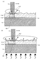
다음에, 레이저 광(14)을 조사한 영역을 용융시키면서 주사하여 산소의 외방 확산을 행한다(도 4a 참조).Next, scanning is performed while melting the area irradiated with the
레이저 광의 조사 영역은 적어도 반도체 소자(트랜지스터 등)를 형성하는 영역이라면 좋다. 단결정 반도체층 전체 면에 레이저 광을 조사하여도 좋다.The irradiation area of the laser light may be at least an area for forming a semiconductor element (transistor or the like). Laser light may be irradiated to the entire surface of the single crystal semiconductor layer.
레이저 광(14)의 종류로서는, 단결정 반도체층에 흡수되는 파장의 레이저 광이면 어느 레이저 광이라도 사용할 수 있다(예를 들어, 엑시머 레이저 광, YAG 레이저 광, YVO4 레이저 광 등).As the kind of the
레이저 광(14)의 조사 영역의 형상도 어느 형상이라도 좋다(예를 들어, 스폿 형상, 선 형상, 면 형상 등).The shape of the irradiation area of the
또한, 레이저 광의 조사 영역의 형상이 면 형상이고, 원하는 영역을 한번에 용융시킬 수 있으면 레이저 광을 주사하지 않아도 좋다.In addition, as long as the shape of the irradiation area of the laser light is planar and the desired area can be melted at once, the laser light may not be scanned.
또한, 펄스 레이저 광을 주사하면서 조사하는 경우는 충분히 가열하기 위하여 조사 영역을 중첩하여 주사하면 바람직하다(특히, 하나의 위치에 펄스 레이저 광이 평균하여 5회 내지 50회 조사되도록 펄스 레이저 광을 주사하면 바람직함).In addition, in the case of irradiating while scanning the pulsed laser light, it is preferable to scan the overlapping irradiation region in order to sufficiently heat (in particular, scan the pulsed laser light so that the pulsed laser light is irradiated 5 to 50 times on average in one position). Preferably).
산소의 외방 확산을 행하는 공정은 표면의 평탄성을 향상시키는 공정과 동시에 행하여도 좋고, 따로 행하여도 좋다(표면의 평탄성의 향상을 다른 공정에서 행하는 경우도 레이저 광(14)과 같은 종류의 레이저 광을 적용할 수 있음).The step of outward diffusion of oxygen may be performed simultaneously with the step of improving the flatness of the surface, or may be performed separately (when the improvement of the surface flatness is performed in another step, the same type of laser light as the
도 4a에서는, 산소의 외방 확산을 행하는 공정과 표면의 평탄성을 향상시키는 공정을 동시에 행한다.In FIG. 4A, a step of outward diffusion of oxygen and a step of improving surface flatness are performed at the same time.
레이저 광(14)이 조사된 개소는 용융 상태의 반도체(11d)가 된다.The part irradiated with the
용융 상태의 반도체(11d)는 고상 상태의 반도체보다 산소의 확산 계수가 높 아지고, 또 레이저 광(14)의 조사에 의하여 온도가 상승되어 산소의 외방 확산이 촉진된다(도 4a의 파선(80) 참조).The
여기서, 접합층(12)이 산소를 함유한 절연막인 경우, 용융 상태의 반도체가 산소를 함유한 절연막과 접촉되면, 산소를 함유한 절연막 중의 산소가 용융 상태인 반도체 중에 확산되어 버리는 문제가 생긴다.Here, in the case where the
따라서, 단결정 반도체층과 접촉되는 절연막이 산소를 함유한 절연막의 경우는 단결정 반도체층의 바닥 부분이 고상 상태가 되는 에너지 밀도로 레이저 광을 조사하는 것이 바람직하다(도 4a 파선(90) 참조).Therefore, in the case where the insulating film in contact with the single crystal semiconductor layer contains oxygen, it is preferable to irradiate laser light at an energy density such that the bottom portion of the single crystal semiconductor layer is in a solid state (see FIG. 4A broken line 90).
즉, 레이저 광을 조사함으로써 단결정 반도체층을 부분 용융시키는 것이 바람직하다.That is, it is preferable to partially melt the single crystal semiconductor layer by irradiating laser light.
부분 용융이란, 단결정 반도체층의 바닥 부분이 고상 상태가 되고, 상기 바닥 부분보다 위의 영역이 용융 상태가 되는 것을 가리킨다.Partial melting means that the bottom part of a single crystal semiconductor layer becomes a solid state, and the area | region above the bottom part becomes a molten state.
왜냐하면, 레이저 광을 조사하여 단결정 반도체층을 부분 용융함으로써 용융 상태의 반도체와 비교하여 산소의 확산 계수가 낮은 고상 상태의 반도체를 용융 상태의 반도체와 산소를 함유한 절연막 사이에 개재시킬 수 있으므로, 산소를 함유한 절연막 중의 산소가 용융 상태의 반도체 중에 확산되어 버리는 것을 방지할 수 있기 때문이다.This is because, by irradiating laser light and partially melting the single crystal semiconductor layer, the semiconductor in the solid state having a lower diffusion coefficient of oxygen than the semiconductor in the molten state can be interposed between the semiconductor in the molten state and the insulating film containing oxygen. This is because the oxygen in the insulating film containing can be prevented from diffusing into the semiconductor in the molten state.
또한, 하지에 함유된 산소가 용융 상태의 반도체 중에 확산되는 문제는 베이스 기판에 단결정 반도체층을 직접 접착하는 경우에 있어서, 베이스 기판이 유리 기판, 석영 기판 등의 산소를 함유한 기판인 경우에도 생기는 문제다.In addition, the problem that oxygen contained in the base diffuses into the semiconductor in the molten state is caused even when the base substrate is a substrate containing oxygen such as a glass substrate or a quartz substrate when the single crystal semiconductor layer is directly bonded to the base substrate. It's a problem.
여기서, 결정 반도체층의 바닥 부분이 고상 상태가 되는 에너지 밀도의 결정 방법에 대하여 설명한다.Here, a method of determining the energy density at which the bottom portion of the crystalline semiconductor layer is in a solid state will be described.
우선, 미리 에너지 밀도를 변화시켜 레이저 광을 조사한 SOI 기판으로 이루어진 복수의 샘플을 준비한다.First, a plurality of samples made of an SOI substrate irradiated with laser light by varying the energy density in advance are prepared.
다음에, 복수의 샘플에 대하여, 반도체층의 단면의 전자 현미경 사진의 관찰, 반도체층의 SIMS 분석(2차 이온 질량 분석) 등을 행한다.Next, observation of the electron micrograph of the cross section of a semiconductor layer, SIMS analysis (secondary ion mass spectrometry), etc. of a semiconductor layer are performed with respect to a some sample.
예를 들어, 반도체층의 단면의 전자 현미경 사진의 관찰을 행하면, 반도체층의 결정화 상태로부터 용융한 깊이를 판단할 수 있다.For example, when the electron micrograph of the cross section of a semiconductor layer is observed, the depth melted from the crystallization state of a semiconductor layer can be judged.
또한, 용융 상태와 고상 상태의 경계에 불순물(탄소, 질소, 산소 등)이 모이기 쉬우므로, SIMS 분석을 하면 불순물 농도가 높은 피크의 위치가 용융 상태와 고상 상태의 경계인 것을 판단할 수 있다.In addition, impurities (carbon, nitrogen, oxygen, etc.) tend to collect at the boundary between the molten state and the solid state, and according to SIMS analysis, it is possible to determine that the peak position having a high impurity concentration is the boundary between the molten state and the solid state.
따라서, 원하는 깊이까지 용융하고자 하는 경우는 미리 복수의 샘플을 형성하여 측정을 해 둠으로써 적절한 에너지 밀도를 결정할 수 있다.Therefore, in the case of melting to a desired depth, an appropriate energy density can be determined by forming a plurality of samples in advance and measuring them.
물론, 에너지 밀도의 결정 방법이 예시한 방법에 한정되지 않는 것은 말할 것도 없다.Of course, it goes without saying that the method of determining the energy density is not limited to the illustrated method.
또한, 도 4a에서는 베이스 기판(13)을 가열하지 않고 레이저 광을 조사하였지만, 도 4b와 같이 베이스 기판(13)을 가열하면서 레이저 광을 조사하면 바람직하다.In addition, although the laser beam was irradiated in FIG. 4A without heating the
즉, 베이스 기판을 가열한 상태에서 레이저 광을 조사하면 단결정 반도체층도 가열된다.That is, when the laser light is irradiated while the base substrate is heated, the single crystal semiconductor layer is also heated.
그리고, 단결정 반도체층이 가열된 상태가 되면, 용융된 단결정 반도체층의 냉각 속도가 완화되기 때문에, 단결정 반도체층의 용융 시간을 길게 할 수 있다.When the single crystal semiconductor layer is in a heated state, the cooling rate of the molten single crystal semiconductor layer is moderated, so that the melting time of the single crystal semiconductor layer can be increased.
단결정 반도체층의 용융 시간이 길어지면, 산소의 확산 계수가 높은 용융 상태의 유지 시간이 길어지기 때문에, 산소의 외방 확산을 더 촉진할 수 있다.The longer the melting time of the single crystal semiconductor layer, the longer the holding time of the molten state in which the oxygen diffusion coefficient is high, so that the outward diffusion of oxygen can be further promoted.
따라서, SOI 기판의 베이스 기판을 가열한 상태에서 레이저 광을 조사하는 것은 레이저 광을 조사함으로써 산소의 외방 확산의 촉진 효과를 촉진할 수 있게 되므로 바람직하다.Therefore, irradiating laser light while the base substrate of the SOI substrate is heated is preferable because the promotion effect of outward diffusion of oxygen can be promoted by irradiating the laser light.
베이스 기판의 온도가 500℃ 이상이면 베이스 기판을 가열하지 않는 경우와 비교하여 산소를 저감할 수 있다.When the temperature of the base substrate is 500 ° C. or more, oxygen can be reduced as compared with the case where the base substrate is not heated.
그리고, 베이스 기판의 온도가 높으면 높을수록 용융 상태의 반도체의 냉각 속도를 느리게 할 수 있으므로, 베이스 기판의 온도는 높을수록 바람직하다.The higher the temperature of the base substrate is, the slower the cooling rate of the semiconductor in the molten state is. Therefore, the higher the temperature of the base substrate is, the better.
또한, 반도체층은 고상 상태라도 온도가 높으면 약간의 산소의 외방 확산이 생기므로, 산소의 외방 확산이 더 촉진된다고 할 수 있다(도 4b의 파선(80) 참조).In addition, even if the semiconductor layer is in a solid state, if the temperature is high, some outward diffusion of oxygen occurs, so that the outward diffusion of oxygen can be further promoted (see dashed
다만, 베이스 기판의 온도가 베이스 기판의 융점 이상이 되면 베이스 기판이 녹아 버린다.However, when the temperature of the base substrate is equal to or higher than the melting point of the base substrate, the base substrate melts.
또한, 베이스 기판의 온도가 베이스 기판의 변형점 온도 이상이 되면 베이스 기판이 변형되어 버린다.Moreover, when the temperature of a base substrate becomes more than the strain point temperature of a base substrate, a base substrate will deform | transform.
따라서, 베이스 기판의 온도 범위의 상한 값은 베이스 기판의 융점보다 낮은 온도, 또는, 베이스 기판의 변형점 온도보다 낮은 온도 중에서 선택하는 것이 바람직하다.Therefore, the upper limit of the temperature range of the base substrate is preferably selected from a temperature lower than the melting point of the base substrate or a temperature lower than the strain point temperature of the base substrate.
다만, 단결정 반도체층이 실리콘인 경우, 실리콘의 융점은 약 1414℃이므로, 베이스 기판의 내열 온도(융점, 변형점 온도 등)가 1414℃ 이상이라도 베이스 기판의 온도는 1414℃보다 낮은 온도로 할 필요가 있다(즉, 베이스 기판의 온도 범위의 상한 값은 단결정 반도체층의 융점 미만의 온도라고 할 수 있음).However, when the single crystal semiconductor layer is silicon, since the melting point of silicon is about 1414 ° C, even if the heat resistance temperature (melting point, strain point temperature, etc.) of the base substrate is 1414 ° C or higher, the temperature of the base substrate should be lower than 1414 ° C. (That is, the upper limit of the temperature range of the base substrate can be said to be a temperature below the melting point of the single crystal semiconductor layer).
또한, 베이스 기판의 온도 범위의 상한 값은 600℃ 이하(또는 600℃ 미만), 650℃ 이하(또는 650℃ 미만), 700℃ 이하(또는 700℃ 미만), 750℃ 이하(또는 750℃ 미만), 800℃ 이하(또는 800℃ 미만), 850℃ 이하(또는 850℃ 미만), 900℃ 이하(또는 900℃ 미만), 950℃ 이하(또는 950℃ 미만), 1000℃ 이하(또는 1000℃ 미만), 1050℃ 이하(또는 1050℃ 미만), 1100℃ 이하(또는 1100℃ 미만), 1150℃ 이하(또는 1150℃ 미만), 1200℃ 이하(또는 1200℃ 미만), 1250℃ 이하(또는 1250℃ 미만), 1300℃ 이하(또는 1300℃ 미만), 1350℃ 이하(또는 1350℃ 미만), 1400℃ 이하(또는 1400℃ 미만) 중에서 선택하여도 좋다. 또한, X℃ 미만이란, X℃보다 낮은 온도를 가리킨다(X는 임의의 수임).In addition, the upper limit of the temperature range of the base substrate is 600 ° C. or less (or less than 600 ° C.), 650 ° C. or less (or less than 650 ° C.), 700 ° C. or less (or less than 700 ° C.), 750 ° C. or less (or less than 750 ° C.). , 800 ° C or less (or less than 800 ° C), 850 ° C or less (or less than 850 ° C), 900 ° C or less (or less than 900 ° C), 950 ° C or less (or less than 950 ° C), 1000 ° C or less (or less than 1000 ° C) , 1050 ° C or less (or less than 1050 ° C), 1100 ° C or less (or less than 1100 ° C), 1150 ° C or less (or less than 1150 ° C), 1200 ° C or less (or less than 1200 ° C), 1250 ° C or less (or less than 1250 ° C) Or 1300 ° C. or less (or less than 1300 ° C.), 1350 ° C. or less (or less than 1350 ° C.), or 1400 ° C. or less (or less than 1400 ° C.). In addition, less than X degreeC means the temperature lower than X degreeC (X is arbitrary number).
또한, 베이스 기판의 온도 범위의 하한 값은 500℃ 이상(또는 500℃ 초과), 550℃ 이상(또는 550℃ 초과), 600℃ 이상(또는 600℃ 초과), 650℃ 이상(또는 650℃ 초과), 700℃ 이상(또는 700℃ 초과), 750℃ 이상(또는 750℃ 초과), 800℃ 이상(또는 800℃ 초과), 850℃ 이상(또는 850℃ 초과), 900℃ 이상(또는 900℃ 초과), 950℃ 이상(또는 950℃ 초과), 1000℃ 이상(또는 1000℃ 초과), 1050℃ 이상(또는 1050℃ 초과), 1100℃ 이상(또는 1100℃ 초과), 1150℃ 이상(또는 1150℃ 초과), 1200℃ 이상(또는 1200℃ 초과), 1250℃ 이상(또는 1250℃ 초과), 1300℃ 이상 (또는 1300℃ 초과), 1350℃ 이상(또는 1350℃ 초과) 중에서 선택하여도 좋다. 또한, X℃ 초과란, X℃보다 높은 온도를 가리킨다(X는 임의의 수임).In addition, the lower limit of the temperature range of the base substrate is at least 500 ° C (or more than 500 ° C), at least 550 ° C (or more than 550 ° C), at least 600 ° C (or more than 600 ° C), at least 650 ° C (or more than 650 ° C). , At least 700 ° C (or above 700 ° C), at least 750 ° C (or above 750 ° C), at least 800 ° C (or above 800 ° C), at least 850 ° C (or above 850 ° C), at least 900 ° C (or above 900 ° C) , At least 950 ° C (or above 950 ° C), at least 1000 ° C (or above 1000 ° C), at least 1050 ° C (or above 1050 ° C), at least 1100 ° C (or above 1100 ° C), at least 1150 ° C (or above 1150 ° C) Or at least 1200 ° C (or more than 1200 ° C), 1250 ° C or more (or more than 1250 ° C), 1300 ° C or more (or more than 1300 ° C), or 1350 ° C or more (or more than 1350 ° C). In addition, over X degreeC refers to temperature higher than X degreeC (X is arbitrary number).
다만, 베이스 기판의 온도 범위의 상한 값은 베이스 기판의 온도 범위의 하한 값보다 큰 것으로 한다.However, the upper limit of the temperature range of a base substrate shall be larger than the lower limit of the temperature range of a base substrate.
베이스 기판의 가열 수단으로서는 접촉 가열, 광 조사에 의한 가열, 유도 가열 등의 수단이 있다.As a heating means of the base substrate, there are means such as contact heating, heating by light irradiation, induction heating and the like.
접촉 가열은 기판을 배치하는 스테이지 등을 가열하여 스테이지 등과 접촉되는 기판을 가열하는 수단이다.The contact heating is a means for heating a substrate on which the substrate is placed and the like to heat the substrate in contact with the stage.
따라서, 접촉 가열을 사용하면 베이스 기판이 어느 종류의 기판이라도 가열할 수 있다.Therefore, when contact heating is used, any kind of substrate can be heated.
한편, 광 조사에 의한 가열은 기판에 흡수되는 파장의 광을 기판에 조사하여 기판을 발열시키는 수단이다.On the other hand, heating by light irradiation is a means for radiating the substrate with light having a wavelength absorbed by the substrate to generate heat.
따라서, 광 조사에 의한 가열을 사용하는 경우는 베이스 기판의 종류와 광 파장의 선택이 필수적이다.Therefore, when using heating by light irradiation, selection of the kind of base substrate and light wavelength is essential.
광 조사에 의한 가열로서는, 예를 들어, 베이스 기판을 실리콘을 주성분으로 하는 기판으로 하고, 광을 실리콘에 흡수되는 광(레이저 광, 램프 광(텅스텐 할로겐 램프 등) 등)으로 하는 방법 등이 있다.As a heating by light irradiation, the base substrate is made into the board | substrate which has silicon as a main component, and the method of making light into the light (laser light, lamp light (tungsten halogen lamp etc.) etc.) absorbed by silicon, etc. are mentioned, for example. .
레이저 광(제 2 레이저 광으로 함)은 산소 확산을 위한 레이저 광(14(제 1 레이저 광))과 같은 것을 사용할 수 있다. 예를 들어, 베이스 기판을 용융시키지 않는 에너지 밀도로 베이스 기판 측으로부터 조사한다.As the laser light (second laser light), one such as laser light 14 (first laser light) for oxygen diffusion can be used. For example, it irradiates from the base substrate side with the energy density which does not melt a base substrate.
이 경우, 제 1 레이저 광을 단결정 반도체층 측으로부터 조사하고 제 2 레이저 광을 베이스 기판 측으로부터 조사함과 함께, 제 1 레이저 광의 조사 영역의 일부분과 제 2 레이저 광의 조사 영역의 일부분이 중첩되도록 한다. 또한, 제 1 레이저 광의 파장과 제 2 레이저 광의 파장이 상이하면 제 2 레이저 광을 단결정 반도체층 측으로부터 조사하여도 처리할 수 있다.In this case, the first laser light is irradiated from the single crystal semiconductor layer side and the second laser light is irradiated from the base substrate side, and a part of the irradiation area of the first laser light and a part of the irradiation area of the second laser light are overlapped. . If the wavelength of the first laser light is different from the wavelength of the second laser light, the second laser light can be processed even when irradiated from the single crystal semiconductor layer side.
또한, 제 1 레이저 광과 제 2 레이저 광의 주사 방향이 같은 방향을 향하도록 주사한다.Further, scanning is performed so that the scanning directions of the first laser light and the second laser light face the same direction.
또한, 제 2 레이저 광은 여열(余熱)용이므로, 제 2 레이저 광의 조사 영역의 면적이 제 1 레이저 광의 조사 영역의 면적보다 크게 되도록 하면 바람직하다.In addition, since the second laser light is for the heat of use, it is preferable to make the area of the irradiation area of the second laser light larger than the area of the irradiation area of the first laser light.
제 2 레이저 광의 조사 영역의 면적이 제 1 레이저 광의 조사 영역의 면적보다 크게 되도록 함으로써, 여열 범위를 광범위하게 할 수 있으므로, 용융 상태를 유지할 수 있는 영역을 광범위하게 할 수 있기 때문이다.This is because, by making the area of the irradiation area of the second laser light larger than the area of the irradiation area of the first laser light, the range of the extra heat can be broadened, so that the area in which the molten state can be maintained can be widened.
또한, 제 2 레이저 광은 단결정 반도체층과 비교하여 매우 두꺼운 베이스 기판을 조사하는 것이다.Further, the second laser light is to irradiate a very thick base substrate as compared with the single crystal semiconductor layer.
따라서, 제 2 레이저 광에는 제 1 레이저 광보다 파장이 긴 레이저 광을 사용하는 것이 바람직하다.Therefore, it is preferable to use laser light with a longer wavelength than the first laser light for the second laser light.
레이저 광의 파장이 길면, 피조사물 표면으로부터 깊은 위치까지 레이저 광이 조사되기 때문이다.This is because when the wavelength of the laser light is long, the laser light is irradiated from the surface of the irradiated object to a deep position.
유도 가열은 교류 자장 중에 도체를 놓고, 도체에 와 전류(eddy current)를 발생시켜 도체를 발열시키는 방법이다.Induction heating is a method of placing a conductor in an alternating magnetic field and generating a eddy current in the conductor to generate heat.
따라서, 유도 가열이 가능한 베이스 기판은 와 전류가 흐르기 쉬운 도체인 것이 바람직하다.Therefore, the base substrate capable of induction heating is preferably a conductor in which eddy currents easily flow.
와 전류가 흐르기 쉬운 것은 어느 정도 저항이 높은 도체이므로, 유도 가열을 사용하는 경우는 베이스 기판으로서 실리콘 웨이퍼, 철 기판, 스테인리스 기판 등을 사용하는 것이 바람직하다.Since the eddy current easily flows to some extent, the conductor has a high resistance, so when using induction heating, it is preferable to use a silicon wafer, an iron substrate, a stainless steel substrate, or the like as the base substrate.
접촉 가열은 베이스 기판이 원하는 온도에 도달될 때까지 시간이 걸리기 때문에, 베이스 기판이 원하는 온도에 도달될 때까지 시간이 짧은 광 조사에 의한 가열, 유도 가열 등을 사용하면 처리 시간을 단축할 수 있다. 또한, 유도 가열로 도체를 가열하고, 도체로부터의 열 전도를 이용한 가열 방법을 사용하여도 좋다.Since the contact heating takes time until the base substrate reaches the desired temperature, the processing time can be shortened by using heating by short time light irradiation, induction heating, etc. until the base substrate reaches the desired temperature. . In addition, the conductor may be heated by induction heating, and a heating method using heat conduction from the conductor may be used.
또한, 레이저 광의 조사 분위기를 불활성 기체 분위기(질소, 희 가스 등)로 함으로써 분위기 중으로부터 산소가 혼입되는 것을 방지할 수 있어 바람직하다.In addition, by making the irradiation atmosphere of laser light into an inert gas atmosphere (nitrogen, rare gas, etc.), it is possible to prevent oxygen from being mixed in the atmosphere.
또한, 레이저 광의 조사 분위기를 감압 분위기(기압이 10-3Pa 이하의 분위기)로 함으로써, 분위기 중으로부터 산소가 혼입되는 것을 방지할 수 있어 바람직하다.Moreover, since the irradiation atmosphere of a laser beam is made into the reduced pressure atmosphere (atmosphere whose atmospheric pressure is 10-3 Pa or less), oxygen can be prevented from mixing in an atmosphere, and it is preferable.
또한, 레이저 광의 조사 분위기를 환원 분위기(수소를 함유한 분위기, 일산화탄소를 함유한 분위기, 요오드화 수소를 함유한 분위기 등(환원 가스만이라도 좋고, 환원 가스와 불활성 기체의 혼합 가스라도 좋음))으로 함으로써 환원 반응이 생기므로, 산소의 외방 확산을 촉진할 수 있어 바람직하다.Further, the laser beam irradiation atmosphere is reduced by reducing the atmosphere (atmosphere containing hydrogen, atmosphere containing carbon monoxide, atmosphere containing hydrogen iodide, or the like (reduced gas may be sufficient or mixed gas of reducing gas and inert gas)). Since a reaction occurs, the outward diffusion of oxygen can be promoted, which is preferable.
즉, 레이저 광의 조사 분위기에 환원 가스를 포함시키면 바람직하다.That is, it is preferable to include a reducing gas in the irradiation atmosphere of a laser beam.
특히, 요오드화 수소를 함유한 분위기는 환원 작용이 있는 동시에 할로겐인 요오드에 의하여 중금속 등의 오염을 제거할 수 있어 바람직하다.In particular, an atmosphere containing hydrogen iodide is preferable because it has a reducing effect and can remove contamination such as heavy metals by iodine which is halogen.
또한, 감압 분위기 또 불활성 기체 분위기, 또는 감압 분위기 또 환원 분위기로 하면, 산소 저감 효과가 더 높아지므로 바람직하다.Moreover, when it is set as a reduced pressure atmosphere, an inert gas atmosphere, or a reduced pressure atmosphere, or a reducing atmosphere, since oxygen reduction effect becomes higher, it is preferable.
또한, 레이저 광을 조사하기 전에 불화 수소 용액을 사용하여 반도체층의 자연 산화막을 제거해 두는 것이 바람직하다.Moreover, it is preferable to remove the natural oxide film of a semiconductor layer using a hydrogen fluoride solution before irradiating a laser beam.
자연 산화막은 불균일하게 형성되기 때문에, 자연 산화막이 존재하면 레이저 광을 조사한 후의 반도체막의 결정 상태에 불균일이 생기기 때문이다. 또한, 산소가 자연 산화막으로부터 반도체층으로 확산되는 것을 방지하기 위해서이다.This is because the native oxide film is formed nonuniformly, and therefore, the presence of the native oxide film causes nonuniformity in the crystal state of the semiconductor film after laser light irradiation. This is to prevent oxygen from diffusing from the natural oxide film into the semiconductor layer.
한편, 공정수를 삭감하기 위하여, 불화 수소 용액을 사용하는 대신에, 감압 분위기, 환원 분위기, 또는 감압 분위기 또 환원 분위기 등의 분위기에 불화 수소를 함유시켜도 좋다.On the other hand, in order to reduce process water, instead of using a hydrogen fluoride solution, you may contain hydrogen fluoride in atmospheres, such as a reduced pressure atmosphere, a reducing atmosphere, or a reduced pressure atmosphere, or a reducing atmosphere.
또한, 대기 분위기, 불활성 기체 분위기(희 가스, 질소 등)에 불화 수소를 함유시켜도 좋다.Moreover, you may make hydrogen fluoride contain in an atmospheric atmosphere and inert gas atmosphere (rare gas, nitrogen, etc.).
물론, 불화 수소 분위기만이라도 좋다.Of course, only hydrogen fluoride atmosphere may be sufficient.
즉, 레이저 광의 조사 분위기에 불화 수소 가스를 포함시키면 바람직하다.That is, it is preferable to include hydrogen fluoride gas in the irradiation atmosphere of a laser beam.
불화 수소는 산화실리콘막을 제거하는 작용이 있기 때문에, 반도체층 표면의 자연 산화막을 제거하면서 레이저 광을 조사할 수 있어 바람직하다.Since hydrogen fluoride has the effect of removing the silicon oxide film, laser light can be irradiated while removing the native oxide film on the surface of the semiconductor layer.
특히, 불화 수소를 함유한 분위기 중에 잠시 SOI 기판을 노출한 직후에 연속적으로 레이저 광을 조사하면, 자연 산화막을 확실히 제거한 후 레이저 광을 조사 할 수 있어 바람직하다(연속적으로 레이저 광을 조사하므로 공정수도 삭감할 수 있음).In particular, continuously irradiating laser light immediately after exposing the SOI substrate in an atmosphere containing hydrogen fluoride is preferable since it is possible to reliably remove the natural oxide film and irradiate the laser light (the process water is also irradiated with laser light continuously). Can be reduced).
또한, 요오드화 수소, 불화 수소 등은 금속을 침식하기 쉬우므로, 요오드화 수소, 불화 수소 등을 분위기에 도입할 때는, 레이저 광의 조사를 행하는 처리실 내의 내벽, 스테이지 등을 사파이어, 다이아몬드 라이크 카본 등으로 코팅해 두면 바람직하다.In addition, since hydrogen iodide, hydrogen fluoride, and the like tend to corrode metals, when introducing hydrogen iodide, hydrogen fluoride, or the like into the atmosphere, the inner walls and stages of the processing chamber where laser light is irradiated are coated with sapphire, diamond-like carbon or the like. It is preferable to leave it.
또한, 레이저 광의 조사 분위기의 온도를 높게 하면, 용융 상태의 유지 시간이 길어져 바람직하다.Moreover, when the temperature of the irradiation atmosphere of a laser beam is made high, the holding time of a molten state will become long and it is preferable.
베이스 기판의 가열 온도가 500℃ 이상인 경우에 산소 저감의 효과가 있는 것을 고려하면, 레이저 광의 조사 분위기의 온도도 500℃ 이상인 것이 바람직하다.When the heating temperature of a base substrate is 500 degreeC or more, considering that there exists an effect of oxygen reduction, it is preferable that the temperature of the laser beam irradiation atmosphere is also 500 degreeC or more.
또한, 레이저 광의 조사 분위기의 온도 범위의 상한 값은 600℃ 이하(또는 600℃ 미만), 650℃ 이하(또는 650℃ 미만), 700℃ 이하(또는 700℃ 미만), 750℃ 이하(또는 750℃ 미만), 800℃ 이하(또는 800℃ 미만), 850℃ 이하(또는 850℃ 미만), 900℃ 이하(또는 900℃ 미만), 950℃ 이하(또는 950℃ 미만), 1000℃ 이하(또는 1000℃ 미만), 1050℃ 이하(또는 1050℃ 미만), 1100℃ 이하(또는 1100℃ 미만), 1150℃ 이하(또는 1150℃ 미만), 1200℃ 이하(또는 1200℃ 미만), 1250℃ 이하(또는 1250℃ 미만), 1300℃ 이하(또는 1300℃ 미만), 1350℃ 이하(또는 1350℃ 미만), 1400℃ 이하(또는 1400℃ 미만) 중에서 선택하여도 좋다. 또한, X℃ 미만이란, X℃보다 낮은 온도를 가리킨다(X는 임의의 수임).In addition, the upper limit of the temperature range of the irradiation atmosphere of a laser beam is 600 degrees C or less (or less than 600 degrees C), 650 degrees C or less (or less than 650 degrees C), 700 degrees C or less (or less than 700 degrees C), 750 degrees C or less (or 750 degrees C.). Less than), 800 ° C. or less (or less than 800 ° C.), 850 ° C. or less (or less than 850 ° C.), 900 ° C. or less (or less than 900 ° C.), 950 ° C. or less (or less than 950 ° C.), 1000 ° C. or less (or 1000 ° C.) Below), 1050 ° C or less (or less than 1050 ° C), 1100 ° C or less (or less than 1100 ° C), 1150 ° C or less (or less than 1150 ° C), 1200 ° C or less (or less than 1200 ° C), 1250 ° C or less (or 1250 ° C) Or less), 1300 ° C or less (or less than 1300 ° C), 1350 ° C or less (or less than 1350 ° C), or 1400 ° C or less (or less than 1400 ° C). In addition, less than X degreeC means the temperature lower than X degreeC (X is arbitrary number).
또한, 레이저 광의 조사 분위기의 온도 범위의 하한 값은 500℃ 이상(또는 500℃ 초과), 550℃ 이상(또는 550℃ 초과), 650℃ 이상(또는 650℃ 초과), 600℃ 이상(또는 600℃ 초과), 650℃ 이상(또는 650℃ 초과), 700℃ 이상(또는 700℃ 초과), 750℃ 이상(또는 750℃ 초과), 800℃ 이상(또는 800℃ 초과), 850℃ 이상(또는 850℃ 초과), 900℃ 이상(또는 900℃ 초과), 950℃ 이상(또는 950℃ 초과), 1000℃ 이상(또는 1000℃ 초과), 1050℃ 이상(또는 1050℃ 초과), 1100℃ 이상(또는 1100℃ 초과), 1150℃ 이상(또는 1150℃ 초과), 1200℃ 이상(또는 1200℃ 초과), 1250℃ 이상(또는 1250℃ 초과), 1300℃ 이상(또는 1300℃ 초과), 1350℃ 이상(또는 1350℃ 초과) 중에서 선택하여도 좋다. 또한, X℃ 초과란, X℃보다 높은 온도를 가리킨다(X는 임의의 수임).Moreover, the lower limit of the temperature range of the irradiation atmosphere of a laser beam is 500 degreeC or more (or more than 500 degreeC), 550 degreeC or more (or more than 550 degreeC), 650 degreeC or more (or more than 650 degreeC), 600 degreeC or more (or 600 degreeC) ), At least 650 ° C (or above 650 ° C), at least 700 ° C (or above 700 ° C), at least 750 ° C (or above 750 ° C), at least 800 ° C (or above 800 ° C), at least 850 ° C (or 850 ° C) ), At least 900 ° C (or above 900 ° C), at least 950 ° C (or above 950 ° C), at least 1000 ° C (or above 1000 ° C), at least 1050 ° C (or above 1050 ° C), at least 1100 ° C (or 1100 ° C) ), At least 1150 ° C (or above 1150 ° C), at least 1200 ° C (or above 1200 ° C), at least 1250 ° C (or above 1250 ° C), at least 1300 ° C (or above 1300 ° C), at least 1350 ° C (or 1350 ° C) Excess). In addition, over X degreeC refers to temperature higher than X degreeC (X is arbitrary number).
다만, 레이저 광의 조사 분위기의 온도 범위의 상한 값은 레이저 광의 조사 분위기의 온도 범위의 하한 값보다 큰 것으로 한다.However, the upper limit of the temperature range of the irradiation atmosphere of laser light shall be larger than the lower limit of the temperature range of the irradiation atmosphere of laser light.
상술한 바와 같이, 산소를 저감시킨 SOI 기판을 형성할 수 있다.As described above, an SOI substrate having reduced oxygen can be formed.
또한, 레이저 광의 조사는 구멍이 발생되는 것을 회피하기 위하여 단결정 반도체층의 막 두께의 평균 값이 100㎚ 이상의 상태에서 행하는 것이 바람직하다.In addition, it is preferable to perform irradiation of a laser beam in the state in which the average value of the film thickness of a single crystal semiconductor layer is 100 nm or more, in order to avoid that a hole generate | occur | produces.
그러나, 축척 법칙(scaling law)에 따르면, 단결정 반도체층의 막 두께가 얇으면 얇을수록 트랜지스터의 특성이 상승되는 것이 알려져 있다.However, according to the scaling law, it is known that the thinner the thickness of the single crystal semiconductor layer, the higher the transistor characteristics.
따라서, 단결정 반도체층의 막 두께를 100㎚보다 얇게 하고 싶은 경우에는 100㎚ 이상의 막 두께로 레이저 광을 조사하고, 레이저 광을 조사한 후에 막 두께를 100㎚보다 얇게 하기 위한 박막화 에칭을 행하면 바람직하다(도 5a 및 도 5b 참조).Therefore, when the film thickness of the single crystal semiconductor layer is to be made thinner than 100 nm, it is preferable to irradiate laser light with a film thickness of 100 nm or more, and to perform a thin film etching for making the film thickness thinner than 100 nm after irradiating the laser light ( 5a and 5b).
또한, 레이저 광을 조사할 때의 단결정 반도체층의 막 두께가 300㎚보다 두꺼우면, 레이저 광을 충분히 흡수할 수 없는 경우가 있으므로, 레이저 광을 조사할 때의 단결정 반도체층의 막 두께가 300㎚ 이하인 것이 바람직하다.In addition, when the film thickness of the single crystal semiconductor layer when irradiating laser light is thicker than 300 nm, laser light may not be sufficiently absorbed, so the film thickness of the single crystal semiconductor layer when irradiating laser light is 300 nm. It is preferable that it is the following.
본 실시형태는 다른 모든 실시형태와 조합하여 실시할 수 있다.This embodiment can be implemented in combination with all other embodiments.
(실시형태 2)(Embodiment 2)
본 실시형태에서는 SOI 기판을 사용하여 형성한 반도체 장치의 제작 방법의 일례에 대하여 설명한다.In this embodiment, an example of the manufacturing method of the semiconductor device formed using the SOI substrate is demonstrated.
우선, 베이스 기판(100)과, 베이스 기판(100) 위에 형성된 접합층(200)과, 접합층(200) 위에 형성된 단결정 반도체층(300)을 갖는 구조의 SOI 기판을 준비한다(도 6a 참조).First, an SOI substrate having a structure having a
베이스 기판, 접합층, 단결정 반도체층은 각각 실시형태 1에 기재한 것과 같은 재료를 사용할 수 있다.As the base substrate, the bonding layer, and the single crystal semiconductor layer, the same materials as those described in
다음에, 단결정 반도체층(300)을 에칭하여 섬 형상으로 가공한다.Next, the single
여기서는, 섬 형상 반도체층(301, 302) 등을 형성한다(소자 분리 공정).Here, island-like semiconductor layers 301 and 302 are formed (element separation step).
그리고, 섬 형상 반도체층(301, 302) 위에 게이트 절연막(400), 게이트 전극(501, 502)을 순차로 형성한다(도 6b 참조).Then, the
게이트 절연막은 열 산화막, 산화실리콘막, 질화실리콘막, 질화산화실리콘막, 산화질화실리콘막, 하프늄 화합물막 등을 사용할 수 있다.As the gate insulating film, a thermal oxide film, a silicon oxide film, a silicon nitride film, a silicon nitride oxide film, a silicon oxynitride film, a hafnium compound film, or the like can be used.
게이트 절연막은 단층과 적층의 어느 쪽이라도 좋다.The gate insulating film may be either a single layer or a laminate.
게이트 전극은 텅스텐, 몰리브덴, 알루미늄, 티타늄, 실리콘 등을 사용할 수 있다.Tungsten, molybdenum, aluminum, titanium, silicon, or the like may be used as the gate electrode.
게이트 전극은 단층과 적층의 어느 쪽이라도 좋다.The gate electrode may be either a single layer or a stack.
다음에, 섬 형상 반도체층(301)에 제 1 불순물 원소를 선택적으로 첨가하여 불순물 영역(301a, 301b)을 형성한다(도 6c 참조).Next, the impurity regions 301a and 301b are formed by selectively adding the first impurity element to the island-like semiconductor layer 301 (see Fig. 6C).
또한, 섬 형상 반도체층(302)에 제 2 불순물 원소를 선택적으로 첨가하여 불순물 영역(302a, 302b)을 형성한다(도 6c 참조).In addition, the impurity regions 302a and 302b are formed by selectively adding the second impurity element to the island-like semiconductor layer 302 (see Fig. 6C).
제 1 불순물 원소와 제 2 불순물 원소는 어느 쪽을 먼저 첨가하여도 좋다.The first impurity element and the second impurity element may be added either first.
또한, 제 1 불순물 원소는 도너 원소(인, 비소 등) 또는 억셉터 원소(붕소 등)의 한쪽이다.In addition, a 1st impurity element is either a donor element (phosphorus, arsenic etc.) or an acceptor element (boron etc.).
또한, 제 2 불순물 원소는 도너 원소(인, 비소 등) 또는 억셉터 원소(붕소 등)의 다른 쪽이다.The second impurity element is the other of the donor element (phosphorus, arsenic, etc.) or the acceptor element (boron, etc.).
또한, 불순물 영역(301a, 301b, 302a, 302b)에는 마스크 또는 사이드 월 등을 사용하여 LDD 영역을 형성하여도 좋다.In the impurity regions 301a, 301b, 302a, and 302b, a LDD region may be formed using a mask or a sidewall.
다음에, 게이트 전극 위에 층간 절연막(600)을 형성하고, 층간 절연막(600)에 콘택트 홀을 형성하고, 층간 절연막(600) 위에 콘택트 홀을 통하여 반도체층 및 게이트 전극과 전기적으로 접속되는 배선(701a 내지 701c, 702a 내지 702c)을 형성한다(도 7a 및 도 7b 참조).Next, an
또한, 도 7a 및 도 7b는 상이한 개소의 단면도이다.7A and 7B are sectional views of different points.
그리고, 게이트 전극과 배선의 콘택트 개소는 게이트 전극 아래에 반도체층이 존재하지 않는 개소로 한다(도 7b 참조).The contact point of the gate electrode and the wiring is a place where the semiconductor layer does not exist below the gate electrode (see FIG. 7B).
층간 절연막은 산화실리콘막, 질화실리콘막, 질소를 함유한 산화실리콘막, 산소를 함유한 질화실리콘막, 폴리이미드, 아크릴, 실록산 폴리머 등을 사용할 수 있다.As the interlayer insulating film, a silicon oxide film, a silicon nitride film, a silicon oxide film containing nitrogen, a silicon nitride film containing oxygen, a polyimide, an acrylic, a siloxane polymer, or the like can be used.
층간 절연막은 단층과 적층의 어느 쪽이라도 좋다.The interlayer insulating film may be either a single layer or a laminate.
배선은 알루미늄, 티타늄, 몰리브덴, 텅스텐, 금, 은, 구리 등의 금속, 또는 ITO(산화인듐주석) 등의 투명 도전물을 사용할 수 있다.As the wiring, a metal such as aluminum, titanium, molybdenum, tungsten, gold, silver, copper, or a transparent conductive material such as ITO (indium tin oxide) can be used.
배선은 단층과 적층의 어느 쪽이라도 좋다.Wiring may be either single layer or lamination.
본 실시형태는 다른 모든 실시형태와 조합하여 실시할 수 있다.This embodiment can be implemented in combination with all other embodiments.
(실시형태 3)(Embodiment 3)
본 실시형태에서는 SOI 기판을 사용하여 형성한 반도체 장치의 제작 방법의 일례에 대하여 설명한다.In this embodiment, an example of the manufacturing method of the semiconductor device formed using the SOI substrate is demonstrated.
우선, 베이스 기판(1100)과, 베이스 기판(1100) 위에 형성된 접합층(1200)과, 접합층(1200) 위에 형성된 단결정 반도체층(1300)을 갖는 구조의 SOI 기판을 준비한다(도 8a 참조).First, an SOI substrate having a structure including a base substrate 1100, a
베이스 기판, 접합층, 단결정 반도체층은 각각 실시형태 1에 기재한 것과 같은 재료를 사용할 수 있다.As the base substrate, the bonding layer, and the single crystal semiconductor layer, the same materials as those described in
다음에, 단결정 반도체층(1300) 위에 섬 형상의 마스크 절연막(1400)을 형성한다(도 8b 참조).Next, an island-shaped
다음에, 마스크 절연막(1400)을 마스크로서 사용하여 단결정 반도체층(1300)을 에칭하여 섬 형상으로 한다(섬 형상 반도체층(1301, 1302) 등을 형성함; 도 8c 참조, 소자 분리 공정).Next, the single
다음에, 마스크 절연막(1400) 위에 절연막을 형성하고, 절연막을 에치 백 또는 연마하여 섬 형상 반도체층 사이를 채우는 매립(embedded) 절연막(1500)을 형성한다(도 9a 참조).Next, an insulating film is formed on the
여기서, 마스크 절연막(1400) 및 매립 절연막(1500)은 산화실리콘막, 질화실리콘막, 질화산화실리콘막, 산화질화실리콘막 등을 사용할 수 있다.The
다만, 마스크 절연막(1400)을 매립 절연막(1500)을 형성할 때의 에칭 스토퍼로서 사용하기 위해서는 마스크 절연막(1400)과 매립 절연막(1500)을 상이한 재질의 막으로 하는 것이 바람직하다.However, in order to use the
다음에, 마스크 절연막(1400)을 제거한다(도 9b 참조).Next, the
다음에, 섬 형상 반도체층(1301) 위에 게이트 절연막(1601)을 형성함과 함께, 섬 형상 반도체층(1302) 위에 게이트 절연막(1602)을 형성한다(도 9c 참조).Next, a gate insulating film 1601 is formed over the island-like semiconductor layer 1301, and a gate insulating film 1602 is formed over the island-shaped semiconductor layer 1302 (see FIG. 9C).
게이트 절연막은 열 산화막, 산화실리콘막, 질화실리콘막, 질화산화실리콘막, 산화질화실리콘막, 하프늄 화합물막 등을 사용할 수 있다.As the gate insulating film, a thermal oxide film, a silicon oxide film, a silicon nitride film, a silicon nitride oxide film, a silicon oxynitride film, a hafnium compound film, or the like can be used.
게이트 절연막은 단층과 적층의 어느 쪽이라도 좋다.The gate insulating film may be either a single layer or a laminate.
다음에, 게이트 절연막 위에 실리콘을 주성분으로 하는 게이트 전극(1701) 및 실리콘을 주성분으로 하는 게이트 전극(1702)을 형성한다(도 10a 참조).Next, a
실리콘을 주성분으로 하는 게이트 전극에는 도너 원소 또는 억셉터 원소를 첨가하여 저항 값을 낮추는 것이 바람직하다.It is preferable to add a donor element or an acceptor element to the gate electrode mainly containing silicon to lower the resistance value.
또한, 도 10a에 도시하는 바와 같이 게이트 전극을 형성할 때, 게이트 절연 막도 동시에 에칭하여 게이트 절연막(1601, 1602)을 형성한다.When the gate electrode is formed as shown in Fig. 10A, the gate insulating film is also simultaneously etched to form the gate insulating films 1601 and 1602.
또한, 게이트 전극은 섬 형상 반도체층과 중첩되는 위치 및 매립 절연막과 중첩되는 위치에 형성된다.The gate electrode is formed at a position overlapping with the island-like semiconductor layer and at a position overlapping with the buried insulating film.
한편, 매립 절연막(1500)은 섬 형상 반도체층과 대략 같은 막 두께가 되도록 형성된다.On the other hand, the buried insulating
따라서, 매립 절연막이 존재함으로써 섬 형상 반도체층의 에지의 단차가 낮아지므로, 섬 형상 반도체층의 에지의 단차로 인하여 게이트 절연막이 단절되어 게이트 전극과 섬 형상 반도체층이 단락되어 버리는 것을 방지할 수 있다.Therefore, the presence of the buried insulating film lowers the level difference between the edges of the island-like semiconductor layers, and therefore, the gate insulating film is disconnected due to the step difference of the edges of the island-like semiconductor layers, thereby preventing the gate electrodes and the island-like semiconductor layers from being shorted. .
또한, 섬 형상 반도체층의 에지는 도 15의 파선(18001, 18002)으로 도시된 부분이다.The edge of the island-like semiconductor layer is a portion shown by broken lines 18001 and 18002 in FIG. 15.
도 15는 섬 형상 반도체층(11301)과, 섬 형상 반도체층(11301)의 주위에 형성된 매립 절연막(11500)과, 섬 형상 반도체층(11301) 및 매립 절연막(11500)과 중첩되는 위치에 배치된 게이트 전극(11701)과, 섬 형상 반도체층(11301)과 배선의 콘택트 영역(12401a, 12401b)과, 게이트 전극과 배선의 콘택트 영역(12401c)을 도시한 것이다.15 is disposed at a position overlapping the island-like semiconductor layer 11301, the buried insulating film 11500 formed around the island-shaped semiconductor layer 11301, and the island-shaped semiconductor layer 11301 and the buried insulating film 11500. The gate electrode 11701, the island-like semiconductor layer 11301, the contact regions 12401a and 12401b of the wiring, and the contact regions 12401c of the gate electrode and the wiring are illustrated.
다음에, 게이트 전극(1701, 1702), 섬 형상 반도체층(1301, 1302)을 산화하여 산화막(1801) 및 산화막(1802)을 형성한다(도 10b 참조).Next, the
또한, 산화막 대신에 질화막을 형성하여도 좋고, 산화와 질화를 동시에 행한 절연막으로 하여도 좋다.In addition, a nitride film may be formed instead of the oxide film, or may be an insulating film in which oxidation and nitride are performed at the same time.
다음에, 섬 형상 반도체층(1301)의 얕은 깊이에 억셉터 원소(붕소)를 선택적 으로 첨가하여 저농도 불순물 영역(1311a, 1311b)을 형성한다(도 10c 참조).Next, acceptor elements (boron) are selectively added to the shallow depth of the island-like semiconductor layer 1301 to form the low concentration impurity regions 1311a and 1311b (see FIG. 10C).
또한, 섬 형상 반도체층(1302)의 얕은 깊이에 도너 원소(비소)를 선택적으로 첨가하여 저농도 불순물 영역(1312a, 1312b)을 형성한다(도 10c 참조).Further, a donor element (arsenic) is selectively added to the shallow depth of the island-
여기서, 인이 아니라 비소를 첨가하는 이유는 활성화 처리시의 열 확산을 억제하기 위하여 확산 계수가 낮은 원소를 사용하기 때문이다.The reason why arsenic is added instead of phosphorus is that an element having a low diffusion coefficient is used to suppress thermal diffusion during the activation process.
열이 확산되는 것을 상관하지 않으면 인을 사용하여도 좋다.Phosphorus may be used if it does not care that heat is diffused.
또한, 도너 원소와 억셉터 원소는 어느 쪽을 먼저 첨가하여도 좋다.In addition, you may add a donor element and an acceptor element first.
다음에, 게이트 전극(1701)을 덮는 사이드 월 형성용 절연막(1901)과, 게이트 전극(1702)을 덮는 사이드 월 형성용 절연막(1902)과, 사이드 월 형성용 절연막(1901, 1902) 위에 형성된 사이드 월 형성용 절연막(1903)을 형성한다(도 11a 참조).Next, the sidewall forming insulating
다음에, 사이드 월 형성용 절연막을 에치 백하여, 사이드 월(1901a, 1901b, 1902a, 1902b, 1903a, 1903b)을 형성한다(도 11b 참조).Next, the side wall forming insulating film is etched back to form side walls 1901a, 1901b, 1902a, 1902b, 1903a, and 1903b (see Fig. 11B).
또한, 사이드 월(1901a, 1901b)은 사이드 월 형성용 절연막(1901)을 에칭하여 형성한 것이고, 사이드 월(1902a, 1902b)은 사이드 월 형성용 절연막(1902)을 에칭하여 형성한 것이고, 사이드 월(1903a, 1903b)은 사이드 월 형성용 절연막(1903)을 에칭하여 형성한 것이다.The sidewalls 1901a and 1901b are formed by etching the sidewall forming insulating
사이드 월 형성용 절연막은 산화실리콘막, 질화실리콘막, 질화산화실리콘막, 산화질화실리콘막 등을 사용할 수 있다.As the sidewall forming insulating film, a silicon oxide film, a silicon nitride film, a silicon nitride oxide film, a silicon oxynitride film, or the like can be used.
다만, 게이트 전극(1701)의 측벽에 형성되는 사이드 월의 폭을 게이트 전 극(1702)의 측벽에 형성되는 사이드 월의 폭보다 넓게 하기 위하여, 사이드 월 형성용 절연막(1901)의 막 두께를 사이드 월 형성용 절연막(1902)의 막 두께보다 두껍게 한다.However, in order to make the width of the sidewall formed on the sidewall of the
또한, 게이트 전극(1701)의 측벽에 형성되는 사이드 월의 단면 형상이 L자 형상이 되도록 하기 위하여, 사이드 월 형성용 절연막(1903)의 재료와 사이드 월 형성용 절연막(1901)의 재료를 상이한 것으로 한다.In addition, the material of the side wall forming insulating
사이드 월 형성용 절연막(1901)의 막 두께를 사이드 월 형성용 절연막(1902)의 막 두께보다 두껍게 하고, 또 사이드 월 형성용 절연막(1903)의 재료와 사이드 월 형성용 절연막(1901)의 재료를 상이한 것으로 함으로써, 사이드 월 형성용 절연막(1903)이 마스크로서 기능하므로, 게이트 전극(1701)의 측벽에 형성되는 사이드 월의 단면 형상이 L자 형상이 되고, 사이드 월의 폭을 넓게 할 수 있다.The film thickness of the side wall forming insulating
즉, 사이드 월 형성용 절연막(1901)의 막 두께를 사이드 월 형성용 절연막(1902)의 막 두께보다 두껍게 하고, 또 사이드 월 형성용 절연막(1903)의 재료와 사이드 월 형성용 절연막(1901)의 재료와 상이한 것으로 함으로써, 동일한 에치 백 공정으로 폭이 상이한 사이드 월을 형성할 수 있다.That is, the film thickness of the side wall forming insulating
다음에, 노출된 산화막(1801, 1802)을 제거한다(도 11c 참조).Next, the exposed
또한, 사이드 월 형성시의 에치 백은 노출된 산화막(1801, 1802)을 제거하였을 때, 게이트 전극의 정상이 돌출되는 조건으로 에칭한다(도 11c의 파선(8001, 8002) 참조).The etch back during sidewall formation is etched under the condition that the top of the gate electrode protrudes when the exposed
게이트 전극의 정상이 돌출되어 게이트 전극의 측벽이 일부분 노출됨으로써, 이후의 실리사이드화 공정에 있어서 게이트 전극의 실리사이드화를 촉진할 수 있다.The top of the gate electrode protrudes to partially expose the sidewall of the gate electrode, thereby facilitating silicidation of the gate electrode in a subsequent silicidation process.
구체적으로는, 게이트 전극의 정상이 돌출되므로 금속막과 접촉 면적이 커져, 실리사이드화가 촉진되어 실리사이드 영역의 막 두께를 두껍게 할 수 있다.Specifically, since the top of the gate electrode protrudes, the contact area with the metal film is increased, so that silicide formation is promoted and the film thickness of the silicide region can be thickened.
또한, 도 15의 파선(18003)에 도시하는 바와 같이 게이트 전극의 콘택트부는 섬 형상 반도체층과 중첩되는 위치에서 떨어진 위치에 형성되기 때문에, 실리사이드 영역의 막 두께를 두껍게 하여 게이트 전극의 저저항화를 행하는 것은 바람직하다.In addition, as shown by the broken line 18003 in FIG. 15, since the contact portion of the gate electrode is formed at a position away from the position overlapping with the island-like semiconductor layer, the thickness of the silicide region is increased to reduce the resistance of the gate electrode. It is preferable to carry out.
다음에, 섬 형상 반도체층(1301)에 억셉터 원소(붕소)를 선택적으로 첨가하여 고농도 불순물 영역(1321a, 1321b)을 형성한다(도 12a 참조).Next, the acceptor element (boron) is selectively added to the island-like semiconductor layer 1301 to form high concentration impurity regions 1321a and 1321b (see FIG. 12A).
또한, 섬 형상 반도체층(1302)에 도너 원소(비소)를 선택적으로 첨가하여 고농도 불순물 영역(1322a, 1322b)을 형성한다(도 12a 참조).Further, a donor element (arsenic) is selectively added to the island-
여기서, 인이 아니라 비소를 첨가하는 이유는 활성화 처리시의 열 확산을 억제하기 위하여 확산 계수가 낮은 원소를 사용하기 때문이다.The reason why arsenic is added instead of phosphorus is that an element having a low diffusion coefficient is used to suppress thermal diffusion during the activation process.
또한, 도너 원소와 억셉터 원소는 어느 쪽을 먼저 첨가하여도 좋다.In addition, you may add a donor element and an acceptor element first.
열이 확산되는 것을 상관하지 않으면 인을 사용하여도 좋다.Phosphorus may be used if it does not care that heat is diffused.
다음에, 활성화 처리를 행한다(도 12b 참조).Next, an activation process is performed (see Fig. 12B).
활성화 처리에 의하여 열 확산이 생겨 불순물 원소의 확산이 생긴다(도 12b의 파선(8011a, 8011b, 8012a, 8012b 등 참조).Thermal diffusion causes the diffusion of the impurity element by the activation process (see dashed lines 8011a, 8011b, 8012a, 8012b, and the like in FIG. 12B).
사이드 월의 폭이 짧은 트랜지스터는 확산 계수가 낮은 비소를 첨가해 두면, 확산되는 거리가 짧아지므로 확산으로 인하여 LDD 영역이 손실해 버리는 것을 방지할 수 있다(도 12b의 파손(8011a, 8011b, 8012a, 8012b 참조).In the case of a transistor having a short sidewall width, if arsenic having a low diffusion coefficient is added, the diffusion distance is shortened, so that the LDD region can be prevented from being lost due to diffusion (breakage 8011a, 8011b, 8012a, 8012b).
다음에, 금속막(2000)을 형성하고, 가열 처리를 행함으로써 실리사이드 영역(2001a 내지 2001c, 2002a 내지 2002c)을 형성한다(도 12c 참조).Next, the silicide regions 2001a to 2001c and 2002a to 2002c are formed by forming the
금속막으로서는, 코발트, 니켈, 텅스텐 등을 사용할 수 있다.Cobalt, nickel, tungsten, or the like can be used as the metal film.
여기서, 게이트 전극의 정상을 돌출시킴으로써 실리사이드 영역의 막 두께를 두껍게 할 수 있다.Here, the film thickness of the silicide region can be made thick by protruding the top of the gate electrode.
실리사이드 영역의 막 두께를 두껍게 함으로써 게이트 전극의 저저항화가 가능하다.By increasing the thickness of the silicide region, it is possible to reduce the resistance of the gate electrode.
다음에, 금속막(2000)을 제거하고, 게이트 전극(1701, 1702) 위에 층간 절연막(2100)을 형성하고, 층간 절연막(2100) 위의 게이트 전극(1702) 위에 선택적으로 층간 절연막(2200)을 형성한다(도 13a 참조).Next, the
다음에, 층간 절연막(2200)을 마스크로서 사용하여 층간 절연막(2100)을 에치 백하여 사이드 월(2101a, 2101b)을 형성한다(도 13b 참조).Next, the interlayer insulating film 2100 is etched back using the
다음에, 층간 절연막(2101)을 게이트 전극(1702) 위에 선택적으로 형성하고, 층간 절연막(2101, 2200) 위에 층간 절연막(2300)을 형성한다(도 13c 참조).Next, an
층간 절연막은 산화실리콘막, 질화실리콘막, 질화산화실리콘막, 산화질화실리콘막, 폴리이미드, 아크릴, 실록산 폴리머 등을 사용할 수 있다.As the interlayer insulating film, a silicon oxide film, a silicon nitride film, a silicon nitride oxide film, a silicon oxynitride film, a polyimide, an acrylic, a siloxane polymer, or the like can be used.
다만, 층간 절연막(2200)을 마스크로서 사용하여 층간 절연막(2100)을 에치 백하기 때문에, 층간 절연막(2200)과 층간 절연막(2100)은 상이한 재료로 하는 것 이 바람직하다.However, since the interlayer insulating film 2100 is etched back using the
또한, n채널형 트랜지스터 위에 형성되는 층간 절연막을 인장 응력을 갖게 하고, 또 p채널형 트랜지스터 위에 형성되는 층간 절연막을 압축 응력을 갖게 하면, n채널형 트랜지스터 및 p채널형 트랜지스터의 특성값이 상승된다.Further, when the interlayer insulating film formed on the n-channel transistor has a tensile stress and the interlayer insulating film formed on the p-channel transistor has a compressive stress, the characteristic values of the n-channel transistor and the p-channel transistor are increased. .
따라서, 층간 절연막(2100)을 인장 응력을 갖는 막으로 하고, 층간 절연막(2200)을 압축 응력을 갖는 막으로 하면 바람직하다(다만, 층간 절연막(2100)의 인장 응력의 값은 층간 절연막(2200)의 압축 응력보다 작은 값으로 함).Therefore, it is preferable to use the interlayer insulating film 2100 as a film having a tensile stress and the
다음에, 층간 절연막에 콘택트 홀을 형성하고, 층간 절연막 위에 콘택트 홀을 통하여 트랜지스터와 접속되는 배선(2401a 내지 2401c, 2402a 내지 2402c)을 형성한다(도 14a 참조).Next, a contact hole is formed in the interlayer insulating film, and wirings 2401a to 2401c and 2402a to 2402c are formed on the interlayer insulating film to be connected to the transistor via the contact hole (see Fig. 14A).
또한, 도 14a와 도 14b는 상이한 개소의 단면도이다.14A and 14B are sectional views of different points.
그리고, 게이트 전극과 배선의 콘택트 개소는 게이트 전극 아래에 반도체층이 존재하지 않는 개소로 한다(도 14b).The contact point of the gate electrode and the wiring is a place where the semiconductor layer does not exist under the gate electrode (Fig. 14B).
배선은 알루미늄, 티타늄, 몰리브덴, 텅스텐, 금, 은, 구리 등의 금속, 또는 ITO(산화인듐주석) 등의 투명 도전물을 사용할 수 있다.As the wiring, a metal such as aluminum, titanium, molybdenum, tungsten, gold, silver, copper, or a transparent conductive material such as ITO (indium tin oxide) can be used.
배선은 단층과 적층의 어느 쪽이라도 좋다.Wiring may be either single layer or lamination.
본 실시형태는 다른 모든 실시형태와 조합하여 실시할 수 있다.This embodiment can be implemented in combination with all other embodiments.
(실시예 1)(Example 1)
본 발명자들은 베이스 기판과, 베이스 기판 위에 형성된 절연층(접합층)과, 절연층(접합층) 위에 형성된 단결정 반도체층을 갖는 SOI 구조로 이루어진 샘플을 복수개 준비하여, SIMS 분석(2차 이온 질량 분석)을 행하여 단결정 반도체층 중의 산소의 농도를 측정하는 실험을 행하였다.The inventors prepared a plurality of samples having a SOI structure having a base substrate, an insulating layer (bonded layer) formed on the base substrate, and a single crystal semiconductor layer formed on the insulating layer (bonded layer), SIMS analysis (secondary ion mass spectrometry) Was performed to measure the concentration of oxygen in the single crystal semiconductor layer.
(제 1 설명: 샘플의 제작 방법)(First description: how to make a sample)
우선, 염화수소를 함유한 분위기 중에서 950℃의 온도로 열 산화를 행함으로써 실리콘 웨이퍼의 표면에 열 산화막을 100㎚의 막 두께로 형성하였다.First, a thermal oxidation film was formed to a film thickness of 100 nm on the surface of a silicon wafer by thermal oxidation at a temperature of 950 ° C. in an atmosphere containing hydrogen chloride.
다음에, 열 산화막을 형성한 실리콘 웨이퍼에 질량 분리를 행하지 않는 이온 도핑법을 사용하여 수소를 첨가하였다.Next, hydrogen was added to the silicon wafer on which the thermal oxide film was formed by using an ion doping method in which mass separation was not performed.
또한, 이온 도핑은 수소 가스를 도핑 가스로서 사용하여 가속 전압을 50㎸로 설정하여 행하였다.In addition, ion doping was performed by setting acceleration voltage to 50 kV using hydrogen gas as a doping gas.
다음에, 유리 기판(ASAHI GLASS CO., LTD. AN100 기판)으로 이루어진 베이스 기판을 준비하였다.Next, a base substrate made of a glass substrate (ASAHI GLASS CO., LTD. AN100 substrate) was prepared.
그리고, 베이스 기판의 표면과 열 산화막의 표면을 세정한 후, 베이스 기판의 표면과 열 산화막의 표면을 접합하였다.Then, after cleaning the surface of the base substrate and the surface of the thermal oxide film, the surface of the base substrate and the surface of the thermal oxide film were bonded together.
다음에, 200℃로 2시간의 가열 처리(접합 강화)를 행하고, 이어서 600℃로 2시간의 가열 처리(균열 형성)를 행함으로써 SOI 기판을 형성하였다.Next, an SOI substrate was formed by performing a heat treatment (bonding strengthening) at 200 ° C. for 2 hours and then performing a heat treatment (crack formation) at 600 ° C. for 2 hours.
그 후, SOI 기판의 단결정 반도체층의 표면을 드라이 에칭법에 의하여 에치 백하였다.Thereafter, the surface of the single crystal semiconductor layer of the SOI substrate was etched back by the dry etching method.
에치 백 후의 SOI 기판의 단결정 반도체층의 막 두께의 평균 값은 105㎚이었다.The average value of the film thickness of the single crystal semiconductor layer of the SOI substrate after etch back was 105 nm.
또한, 단결정 반도체층의 막 두께의 평균값은 광학적인 막 두께 측정기(나노 스펙)를 사용하여 복수의 개소를 측정하여 복수의 개소의 평균값으로부터 산출하였다.In addition, the average value of the film thickness of the single crystal semiconductor layer was computed from the average value of several places by measuring several places using the optical film thickness meter (nano spec).
그리고, 상술한 공정과 같은 공정을 거친 복수의 샘플을 형성하였다.And the some sample which passed through the process similar to the above-mentioned process was formed.
(제 2 설명: 샘플의 종류)(Second description: types of samples)
참조 샘플은 레이저 광을 조사하지 않은 샘플이다.The reference sample is a sample not irradiated with laser light.
제 1 샘플은 베이스 기판을 가열하지 않고, 단결정 반도체층에 레이저 광을 조사한 샘플이다.The first sample is a sample in which laser light is irradiated to the single crystal semiconductor layer without heating the base substrate.
제 2 샘플은 베이스 기판의 온도를 300℃로 하여 단결정 반도체층에 레이저 광을 조사한 샘플이다.The second sample is a sample obtained by irradiating laser light to the single crystal semiconductor layer at a temperature of the base substrate of 300 ° C.
제 3 샘플은 베이스 기판의 온도를 500℃로 하여 단결정 반도체층에 레이저 광을 조사한 샘플이다.The third sample is a sample obtained by irradiating laser light on the single crystal semiconductor layer at a temperature of the base substrate of 500 ° C.
또한, 레이저 광의 조사 분위기는 질소 분위기로 하였다.In addition, the irradiation atmosphere of laser light was made into nitrogen atmosphere.
또한, 레이저는 엑시머 레이저를 사용하였다.In addition, the excimer laser was used for the laser.
또한, 레이저 광을 조사할 때 부분 용융하였다.In addition, it partially melted when irradiated with laser light.
또한, 베이스 기판과 접촉되는 스테이지를 가열함으로써 베이스 기판을 접촉 가열하였다.In addition, the base substrate was brought into contact heating by heating the stage in contact with the base substrate.
(제 3 설명: SIMS 측정 결과)(Third description: SIMS measurement results)
참조 샘플(레이저 광이 조사되지 않았음), 제 1 샘플(레이저 광이 조사되었음(실온)), 제 2 샘플(레이저 광이 조사되었음(300℃)), 제 3 샘플(레이저 광이 조사되었음(500℃))의 단결정 반도체층 중의 산소 농도를 측정하기 위하여 SIMS 분 석(2차 이온 질량 분석)을 행하였다.Reference sample (laser light not irradiated), first sample (laser light irradiated (room temperature)), second sample (laser light irradiated (300 ° C.)), third sample (laser light irradiated) SIMS analysis (secondary ion mass spectrometry) was performed to measure the oxygen concentration in the single crystal semiconductor layer (500 ° C.).
참조 샘플(레이저 광이 조사되지 않았음), 제 1 샘플(레이저 광이 조사되었음(실온)), 제 2 샘플(레이저 광이 조사되었음(300℃)), 및 제 3 샘플(레이저 광이 조사되었음(500℃))의 SIMS 측정 결과를 정리한 것을 도 16에 도시한다.Reference sample (laser light not irradiated), first sample (laser light irradiated (room temperature)), second sample (laser light irradiated (300 ° C.)), and third sample (laser light irradiated) Fig. 16 shows the results of the SIMS measurement (same as 500 ° C.).
또한, 참조 샘플(레이저 광이 조사되지 않았음), 제 1 샘플(레이저 광이 조사되었음(실온))을 비교한 것을 도 17에 도시한다.In addition, FIG. 17 shows a comparison between a reference sample (not irradiated with laser light) and a first sample (irradiated with laser light (room temperature)).
또한, 제 1 샘플(레이저 광이 조사되었음(실온)), 제 2 샘플(레이저 광이 조사되었음(300℃)), 제 3 샘플(레이저 광이 조사되었음(500℃))을 비교한 것을 도 18에 도시한다.Also, a comparison is made between the first sample (laser light irradiated (room temperature)), the second sample (laser light irradiated (300 ° C)), and the third sample (laser light irradiated (500 ° C)). 18 is shown.
도 16 내지 도 18에 있어서, 그래프(20000)가 참조 샘플(레이저 광이 조사되지 않았음)의 측정 결과이고, 그래프(20001)가 제 1 샘플(레이저 광이 조사되었음(실온))의 측정 결과이고, 그래프(20002)가 제 2 샘플(레이저 광이 조사되었음(300℃))의 측정 결과이고, 그래프(20003)가 제 3 샘플(레이저 광이 조사되었음(500℃))의 측정 결과이다.16 to 18, the
또한, 도 16 내지 도 18의 그래프 중 부호가 같은 것은 같은 데이터에 의거하는 그래프이다.16 to 18 are the same graphs based on the same data.
또한, 도 16 내지 도 18에 있어서, 1E+n(n은 자연수)은 10의 n승을 뜻한다.16 to 18, 1E + n (n is a natural number) means an n power of 10.
(제 4 설명: 고찰)(4th description: consideration)
우선, 도 16 내지 도 18의 그래프를 어떻게 해석하는지에 대하여 설명한다.First, how to interpret the graph of FIGS. 16-18 is demonstrated.
SIMS 분석에 의하여 검출되는 산소 농도 중, 단결정 반도체층 표면 근방(도 면 중의 막 두께가 0㎚ 내지 20㎚의 범위) 및 단결정 반도체층과 접합층의 계면 근방(도면 중의 막 두께가 80㎚ 내지 105㎚의 범위)은 보통 측정 정밀도가 떨어지는 영역이므로, 단결정 반도체층 중의 산소 농도를 비교하는 경우는 참고가 되지 않는다.In the oxygen concentration detected by SIMS analysis, near the surface of the single crystal semiconductor layer (in the range of 0 nm to 20 nm in film thickness) and near the interface between the single crystal semiconductor layer and the bonding layer (film thickness in the figure is 80 nm to 105 nm). The range of nm) is a region in which measurement accuracy is usually inferior, and thus it is not referred to when comparing the oxygen concentration in the single crystal semiconductor layer.
측정 정밀도가 떨어지는 이유는 녹온(knock-on) 효과의 영향, 단결정 반도체층 표면의 요철의 영향, 단결정 반도체층 표면의 오염의 영향을 생각할 수 있다(오염에 대해서는 SIMS 장치가 청정한 분위기인 크린 룸 밖에 있고, SIMS 분석을 위한 샘플을 청정한 분위기 밖으로 반출했기 때문이라고 생각됨).The reason for the inferior measurement accuracy can be attributed to the influence of the knock-on effect, the unevenness of the surface of the single crystal semiconductor layer, and the influence of contamination of the surface of the single crystal semiconductor layer. And the samples for SIMS analysis were taken out of the clean atmosphere).
따라서, 도면 중의 막 두께가 20㎚ 내지 80㎚의 범위의 산소 농도를 비교하면 좋다.Therefore, what is necessary is just to compare the oxygen concentration of the film thickness in the range of 20 nm-80 nm.
우선, 레이저 광이 조사되지 않은 참조 샘플과, 레이저 광이 조사된 제 1 샘플 내지 제 3 샘플을 비교하면, 적어도 레이저 광을 조사하면 산소 농도가 감소되는 것을 알 수 있다(도 16 참조).First, comparing the reference samples not irradiated with the laser light and the first to third samples irradiated with the laser light, it can be seen that the oxygen concentration is reduced when the laser light is irradiated at least (see FIG. 16).
특히, 레이저 광이 조사되지 않은 참조 샘플과 실온에서 레이저 광이 조사된 제 1 샘플을 비교하여도, 제 1 샘플은 산소 농도가 감소되기 때문에, 기판을 가열하지 않아도 산소 농도의 감소 효과를 얻을 수 있는 것을 알 수 있다(도 16 및 도 17 참조).In particular, even when the reference sample not irradiated with the laser light is compared with the first sample irradiated with the laser light at room temperature, since the oxygen concentration is reduced in the first sample, the oxygen concentration reduction effect can be obtained without heating the substrate. It can be seen that there is (see Figs. 16 and 17).
다음에, 제 1 샘플(레이저 광이 조사되었음(실온)), 제 2 샘플(레이저 광이 조사되었음(300℃)), 제 3 샘플(레이저 광이 조사되었음(500℃))을 비교한다(도 16 및 도 18 참조).Next, the first sample (laser light was irradiated (room temperature)), the second sample (laser light was irradiated (300 ° C.)), and the third sample (laser light was irradiated (500 ° C.)) was compared ( 16 and 18).
제 1 샘플(레이저 광이 조사되었음(실온))과 제 2 샘플(레이저 광이 조사되었음(300℃))은 산소 농도에 거의 차이가 없다.The first sample (laser light irradiated (room temperature)) and the second sample (laser light irradiated (300 ° C)) have almost no difference in oxygen concentration.
한편, 제 1 샘플(레이저 광이 조사되었음(실온))과 제 3 샘플(레이저 광이 조사되었음(500℃))을 비교하면, 제 3 샘플(레이저 광이 조사되었음(500℃))은 산소 농도가 감소되는 것을 알 수 있다.On the other hand, when the first sample (laser light was irradiated (room temperature)) and the third sample (laser light was irradiated (500 ° C)), the third sample (laser light was irradiated (500 ° C)) was oxygen It can be seen that the concentration is reduced.
따라서, 적어도 베이스 기판의 온도를 500℃로 한 상태에서 레이저 광을 조사하면, 산소 농도가 감소되는 것을 알 수 있다.Therefore, it can be seen that the oxygen concentration decreases when the laser light is irradiated with the temperature of the base substrate at least 500 ° C.
상술한 결과에 의거하면, 본 발명자들은 레이저 광을 조사함으로써 산소 농도가 감소된 이유는 단결정 반도체층이 산소의 확산 계수가 높은 용융 상태가 되어 산소의 외방 확산이 촉진되어 산소 농도가 감소되기 때문이라고 생각하였다.Based on the above results, the present inventors found that the oxygen concentration was reduced by irradiating laser light because the single crystal semiconductor layer was in a molten state with a high diffusion coefficient of oxygen, thereby promoting the outward diffusion of oxygen and decreasing the oxygen concentration. Thought.
또한, 본 발명자들은 300℃의 기판 가열은 산소의 감소가 현저하지 않고, 500℃의 기판 가열은 산소의 감소가 현저하므로, 확산 계수가 높은 용융 상태의 유지 시간이 길수록 산소의 외방 확산이 촉진된다고 생각하였다.In addition, the present inventors found that the substrate heating at 300 ° C. does not significantly reduce oxygen, and the substrate heating at 500 ° C. is remarkable in oxygen reduction, so that the longer diffusion time of the molten state with a high diffusion coefficient promotes outward diffusion of oxygen. Thought.
따라서, 기판 가열의 온도가 높을수록 용융 상태의 유지 시간이 길어지는 것이 분명하므로, 500℃보다 높은 온도의 기판 가열을 행하면 산소의 감소가 촉진되는 것은 분명하다.Therefore, the higher the temperature of the substrate heating, the longer the retention time of the molten state is. Therefore, it is clear that the reduction of oxygen is promoted by heating the substrate at a temperature higher than 500 ° C.
따라서, 적어도 레이저 광을 조사함으로써 산소의 외방 확산이 생기므로, 산소 농도를 감소시킬 수 있다고 할 수 있다.Therefore, it can be said that oxygen concentration can be reduced because at least laser radiation causes outward diffusion of oxygen.
또한, 500℃ 이상의 온도로 가열하면서 레이저 광을 조사함으로써 산소의 외방 확산을 촉진할 수 있다고 할 수 있다.In addition, it can be said that the outward diffusion of oxygen can be promoted by irradiating a laser light while heating at a temperature of 500 degreeC or more.
(제 5 설명: 이온 도핑법에 대하여)(Fifth explanation: about the ion doping method)
샘플 제작에 사용한 실리콘 웨이퍼는 산소 농도가 1.0×10¹⁸atom/㎤ 내지 2.0×10¹⁸atom/㎤가 되도록 제어된 실리콘 웨이퍼이었다.The silicon wafer used for sample preparation was a silicon wafer controlled to have an oxygen concentration of 1.0 × 10 18 atoms /
그러나, 참조 샘플의 단결정 반도체층 중의 산소 농도는 2.0×10¹⁸atom/㎤보다 높은 값을 나타냈다.However, the oxygen concentration in the single crystal semiconductor layer of the reference sample exhibited a value higher than 2.0 × 10 18 atoms /
따라서, SOI 기판의 제작 공정 중에서 산소 농도가 상승된 것은 분명하다.Therefore, it is clear that the oxygen concentration was raised during the manufacturing process of the SOI substrate.
산소 농도가 상승한 원인의 하나는 질량 분리를 행하지 않는 이온 도핑법을 사용하여 수소를 첨가하는 공정이다.One cause of the increase in oxygen concentration is a step of adding hydrogen using an ion doping method that does not perform mass separation.
즉, 질량 분리를 행하지 않는 경우는 이온 도핑 처리 챔버 내의 분위기 중에 존재하는 원소를 모두 이온화하여 도핑되어 버린다.That is, when mass separation is not performed, all the elements which exist in the atmosphere in an ion doping process chamber are ionized and doped.
그리고, 대기 중에는 산소가 대량으로 존재하기 때문에, 처리 챔버 내에 산소가 완전히 혼입되지 않도록 챔버 내 분위기를 관리하기 어렵다.And since there exists a large amount of oxygen in air | atmosphere, it is difficult to manage the atmosphere in a chamber so that oxygen may not fully mix in a processing chamber.
따라서, 질량 분리하지 않는 이온 도핑법을 사용하여 수소를 첨가하는 공정을 행하는 경우는, 단결정 반도체층 중에 산소도 동시에 도핑되어 버린다.Therefore, when performing the process of adding hydrogen using the ion doping method which does not separate mass, oxygen will also be doped simultaneously in a single crystal semiconductor layer.
도 1a 내지 도 1c는 SOI 기판의 제작 방법의 일례.1A to 1C show an example of a method for producing an SOI substrate.
도 2a 및 도 2b는 SOI 기판의 제작 방법의 일례.2A and 2B show an example of a method for producing an SOI substrate.
도 3a 내지 도 3c는 SOI 기판의 제작 방법의 일례.3A to 3C show an example of a method for producing an SOI substrate.
도 4a 및 도 4b는 SOI 기판의 제작 방법의 일례.4A and 4B show an example of a method for producing an SOI substrate.
도 5a 및 도 5b는 SOI 기판의 제작 방법의 일례.5A and 5B show an example of a method for producing an SOI substrate.
도 6a 내지 도 6c는 반도체 장치의 제작 방법의 일례.6A to 6C are examples of a method of manufacturing a semiconductor device.
도 7a 및 도 7b는 반도체 장치의 제작 방법의 일례.7A and 7B are examples of a method of manufacturing a semiconductor device.
도 8a 내지 도 8c는 반도체 장치의 제작 방법의 일례.8A to 8C are examples of a method for manufacturing a semiconductor device.
도 9a 내지 도 9c는 반도체 장치의 제작 방법의 일례.9A to 9C are examples of a method for manufacturing a semiconductor device.
도 10a 내지 도 10c는 반도체 장치의 제작 방법의 일례.10A to 10C are examples of a method of manufacturing a semiconductor device.
도 11a 내지 도 11c는 반도체 장치의 제작 방법의 일례.11A to 11C are examples of a method for manufacturing a semiconductor device.
도 12a 내지 도 12c는 반도체 장치의 제작 방법의 일례.12A to 12C are examples of a method for manufacturing a semiconductor device.
도 13a 내지 도 13c는 반도체 장치의 제작 방법의 일례.13A to 13C are examples of a method for manufacturing a semiconductor device.
도 14a 및 도 14b는 반도체 장치의 제작 방법의 일례.14A and 14B are examples of a method for manufacturing a semiconductor device.
도 15는 반도체 장치의 상면도의 일례.15 is an example of a top view of a semiconductor device.
도 16은 SIMS 분석 결과의 일례.16 is an example of a SIMS analysis result.
도 17은 SIMS 분석 결과의 일례.17 is an example of a SIMS analysis result.
도 18은 SIMS 분석 결과의 일례.18 is an example of a SIMS analysis result.
<도면의 주요 부분에 대한 부호의 설명><Explanation of symbols for the main parts of the drawings>
11b: 제 2 영역 11d: 용융 상태의 반도체11b:
12: 접합층 13: 베이스 기판12: bonding layer 13: base substrate
14: 레이저 광 80: 파선14: laser light 80: broken line
90: 파선90: dashed line
Claims (24)
Applications Claiming Priority (2)
| Application Number | Priority Date | Filing Date | Title |
|---|---|---|---|
| JPJP-P-2008-318377 | 2008-12-15 | ||
| JP2008318377 | 2008-12-15 |
Related Child Applications (1)
| Application Number | Title | Priority Date | Filing Date |
|---|---|---|---|
| KR1020160128549A Division KR20160120266A (en) | 2008-12-15 | 2016-10-05 | Manufacturing method of soi substrate and manufacturing method of semiconductor device |
Publications (1)
| Publication Number | Publication Date |
|---|---|
| KR20100069595A true KR20100069595A (en) | 2010-06-24 |
Family
ID=42241035
Family Applications (2)
| Application Number | Title | Priority Date | Filing Date |
|---|---|---|---|
| KR1020090123832A KR20100069595A (en) | 2008-12-15 | 2009-12-14 | Manufacturing method of soi substrate and manufacturing method of semiconductor device |
| KR1020160128549A KR20160120266A (en) | 2008-12-15 | 2016-10-05 | Manufacturing method of soi substrate and manufacturing method of semiconductor device |
Family Applications After (1)
| Application Number | Title | Priority Date | Filing Date |
|---|---|---|---|
| KR1020160128549A KR20160120266A (en) | 2008-12-15 | 2016-10-05 | Manufacturing method of soi substrate and manufacturing method of semiconductor device |
Country Status (5)
| Country | Link |
|---|---|
| US (1) | US8394703B2 (en) |
| JP (1) | JP5610759B2 (en) |
| KR (2) | KR20100069595A (en) |
| CN (1) | CN101752294B (en) |
| SG (2) | SG182208A1 (en) |
Families Citing this family (10)
| Publication number | Priority date | Publication date | Assignee | Title |
|---|---|---|---|---|
| FR2972564B1 (en) * | 2011-03-08 | 2016-11-04 | S O I Tec Silicon On Insulator Tech | METHOD FOR PROCESSING A SEMICONDUCTOR TYPE STRUCTURE ON INSULATION |
| TWI664731B (en) * | 2013-05-20 | 2019-07-01 | 半導體能源研究所股份有限公司 | Semiconductor device |
| US9425063B2 (en) * | 2014-06-19 | 2016-08-23 | Infineon Technologies Ag | Method of reducing an impurity concentration in a semiconductor body, method of manufacturing a semiconductor device and semiconductor device |
| DE112015005339T5 (en) | 2014-11-28 | 2017-08-17 | Semiconductor Energy Laboratory Co., Ltd. | Semiconductor device, module and electronic device |
| JP6850096B2 (en) * | 2015-09-24 | 2021-03-31 | 株式会社半導体エネルギー研究所 | Manufacturing method of semiconductor devices and manufacturing method of electronic devices |
| US10026843B2 (en) * | 2015-11-30 | 2018-07-17 | Taiwan Semiconductor Manufacturing Co., Ltd. | Fin structure of semiconductor device, manufacturing method thereof, and manufacturing method of active region of semiconductor device |
| US11255606B2 (en) * | 2015-12-30 | 2022-02-22 | Mattson Technology, Inc. | Gas flow control for millisecond anneal system |
| JP6579086B2 (en) * | 2016-11-15 | 2019-09-25 | 信越半導体株式会社 | Device forming method |
| SG11201906390SA (en) * | 2017-02-21 | 2019-08-27 | Ev Group E Thallner Gmbh | Method and device for bonding substrates |
| KR20200143143A (en) | 2019-06-14 | 2020-12-23 | 삼성전자주식회사 | Fabrication method of integrated circuit semiconductor device |
Family Cites Families (45)
| Publication number | Priority date | Publication date | Assignee | Title |
|---|---|---|---|---|
| JPS6384013A (en) * | 1986-09-27 | 1988-04-14 | Agency Of Ind Science & Technol | Manufacture of semiconductor crystal layer |
| FR2681472B1 (en) * | 1991-09-18 | 1993-10-29 | Commissariat Energie Atomique | PROCESS FOR PRODUCING THIN FILMS OF SEMICONDUCTOR MATERIAL. |
| TW264575B (en) | 1993-10-29 | 1995-12-01 | Handotai Energy Kenkyusho Kk | |
| US5923962A (en) * | 1993-10-29 | 1999-07-13 | Semiconductor Energy Laboratory Co., Ltd. | Method for manufacturing a semiconductor device |
| US6444506B1 (en) * | 1995-10-25 | 2002-09-03 | Semiconductor Energy Laboratory Co., Ltd. | Method of manufacturing silicon thin film devices using laser annealing in a hydrogen mixture gas followed by nitride formation |
| US6391690B2 (en) * | 1995-12-14 | 2002-05-21 | Seiko Epson Corporation | Thin film semiconductor device and method for producing the same |
| US5970368A (en) | 1996-09-30 | 1999-10-19 | Kabushiki Kaisha Toshiba | Method for manufacturing polycrystal semiconductor film |
| JPH1140501A (en) * | 1997-05-20 | 1999-02-12 | Fujitsu Ltd | Semiconductor device and method for manufacturing it |
| US6534380B1 (en) * | 1997-07-18 | 2003-03-18 | Denso Corporation | Semiconductor substrate and method of manufacturing the same |
| JP3349931B2 (en) * | 1997-10-30 | 2002-11-25 | 松下電器産業株式会社 | Method of manufacturing semiconductor laser device |
| JPH11163363A (en) | 1997-11-22 | 1999-06-18 | Semiconductor Energy Lab Co Ltd | Semiconductor device and its forming method |
| JP2000012864A (en) * | 1998-06-22 | 2000-01-14 | Semiconductor Energy Lab Co Ltd | Manufacture of semiconductor device |
| JP2000082679A (en) * | 1998-07-08 | 2000-03-21 | Canon Inc | Semiconductor substrate and production thereof |
| JP3345363B2 (en) * | 1998-12-07 | 2002-11-18 | 富士通株式会社 | Method for forming polycrystalline silicon thin film and method for manufacturing thin film transistor |
| US7153729B1 (en) * | 1998-07-15 | 2006-12-26 | Semiconductor Energy Laboratory Co., Ltd. | Crystalline semiconductor thin film, method of fabricating the same, semiconductor device, and method of fabricating the same |
| JP4476390B2 (en) * | 1998-09-04 | 2010-06-09 | 株式会社半導体エネルギー研究所 | Method for manufacturing semiconductor device |
| JP3794876B2 (en) * | 1998-09-09 | 2006-07-12 | 松下電器産業株式会社 | Manufacturing method of semiconductor device |
| JP4101409B2 (en) * | 1999-08-19 | 2008-06-18 | シャープ株式会社 | Manufacturing method of semiconductor device |
| US7052943B2 (en) * | 2001-03-16 | 2006-05-30 | Semiconductor Energy Laboratory Co., Ltd. | Method of manufacturing a semiconductor device |
| US7253032B2 (en) * | 2001-04-20 | 2007-08-07 | Semiconductor Energy Laboratory Co., Ltd. | Method of flattening a crystallized semiconductor film surface by using a plate |
| TW544938B (en) * | 2001-06-01 | 2003-08-01 | Semiconductor Energy Lab | Method of manufacturing a semiconductor device |
| US7119365B2 (en) * | 2002-03-26 | 2006-10-10 | Sharp Kabushiki Kaisha | Semiconductor device and manufacturing method thereof, SOI substrate and display device using the same, and manufacturing method of the SOI substrate |
| JP2004006700A (en) * | 2002-03-27 | 2004-01-08 | Seiko Epson Corp | Surface processing method and substrate, film pattern forming method, electro-optical device manufacturing method, electro-optical device, and electronic apparatus |
| JP4610178B2 (en) * | 2002-11-15 | 2011-01-12 | 株式会社半導体エネルギー研究所 | Method for manufacturing semiconductor device |
| JP4759919B2 (en) * | 2004-01-16 | 2011-08-31 | セイコーエプソン株式会社 | Manufacturing method of electro-optical device |
| JP5110772B2 (en) | 2004-02-03 | 2012-12-26 | 株式会社半導体エネルギー研究所 | Manufacturing method of substrate having semiconductor thin film layer |
| US20070117287A1 (en) * | 2005-11-23 | 2007-05-24 | Semiconductor Energy Laboratory Co., Ltd. | Laser irradiation apparatus |
| US7579654B2 (en) * | 2006-05-31 | 2009-08-25 | Corning Incorporated | Semiconductor on insulator structure made using radiation annealing |
| CN101281912B (en) * | 2007-04-03 | 2013-01-23 | 株式会社半导体能源研究所 | Soi substrate and manufacturing method thereof, and semiconductor device |
| KR101440930B1 (en) * | 2007-04-20 | 2014-09-15 | 가부시키가이샤 한도오따이 에네루기 켄큐쇼 | Method of manufacturing soi substrate |
| US7960262B2 (en) * | 2007-05-18 | 2011-06-14 | Semiconductor Energy Laboratory Co., Ltd. | Method for manufacturing semiconductor device by applying laser beam to single-crystal semiconductor layer and non-single-crystal semiconductor layer through cap film |
| US7745268B2 (en) * | 2007-06-01 | 2010-06-29 | Semiconductor Energy Laboratory Co., Ltd. | Method for manufacturing a semiconductor device with irradiation of single crystal semiconductor layer in an inert atmosphere |
| US7776718B2 (en) * | 2007-06-25 | 2010-08-17 | Semiconductor Energy Laboratory Co., Ltd. | Method of manufacturing semiconductor substrate with reduced gap size between single-crystalline layers |
| US7795111B2 (en) * | 2007-06-27 | 2010-09-14 | Semiconductor Energy Laboratory Co., Ltd. | Manufacturing method of SOI substrate and manufacturing method of semiconductor device |
| JP5442224B2 (en) * | 2007-07-23 | 2014-03-12 | 株式会社半導体エネルギー研究所 | Manufacturing method of SOI substrate |
| KR101499175B1 (en) * | 2007-10-04 | 2015-03-05 | 가부시키가이샤 한도오따이 에네루기 켄큐쇼 | Method for manufacturing semiconductor substrate |
| US7799658B2 (en) * | 2007-10-10 | 2010-09-21 | Semiconductor Energy Laboratory Co., Ltd. | Method for manufacturing semiconductor substrate and method for manufacturing semiconductor device |
| WO2009057669A1 (en) * | 2007-11-01 | 2009-05-07 | Semiconductor Energy Laboratory Co., Ltd. | Method for manufacturing photoelectric conversion device |
| US7851318B2 (en) * | 2007-11-01 | 2010-12-14 | Semiconductor Energy Laboratory Co., Ltd. | Semiconductor substrate and method for manufacturing the same, and method for manufacturing semiconductor device |
| US7816232B2 (en) * | 2007-11-27 | 2010-10-19 | Semiconductor Energy Laboratory Co., Ltd. | Method for manufacturing semiconductor substrate and semiconductor substrate manufacturing apparatus |
| JP5248994B2 (en) * | 2007-11-30 | 2013-07-31 | 株式会社半導体エネルギー研究所 | Method for manufacturing photoelectric conversion device |
| JP5286046B2 (en) * | 2007-11-30 | 2013-09-11 | 株式会社半導体エネルギー研究所 | Method for manufacturing photoelectric conversion device |
| JP5248995B2 (en) * | 2007-11-30 | 2013-07-31 | 株式会社半導体エネルギー研究所 | Method for manufacturing photoelectric conversion device |
| US7947523B2 (en) * | 2008-04-25 | 2011-05-24 | Semiconductor Energy Laboratory Co., Ltd. | Method for manufacturing photoelectric conversion device |
| US7943414B2 (en) * | 2008-08-01 | 2011-05-17 | Semiconductor Energy Laboratory Co., Ltd. | Method for manufacturing SOI substrate |
-
2009
- 2009-12-07 SG SG2012044475A patent/SG182208A1/en unknown
- 2009-12-07 SG SG200908120-9A patent/SG162675A1/en unknown
- 2009-12-09 US US12/634,107 patent/US8394703B2/en active Active
- 2009-12-10 JP JP2009280207A patent/JP5610759B2/en not_active Expired - Fee Related
- 2009-12-14 KR KR1020090123832A patent/KR20100069595A/en active Application Filing
- 2009-12-15 CN CN200910262141.XA patent/CN101752294B/en not_active Expired - Fee Related
-
2016
- 2016-10-05 KR KR1020160128549A patent/KR20160120266A/en active Search and Examination
Also Published As
| Publication number | Publication date |
|---|---|
| US20100151663A1 (en) | 2010-06-17 |
| SG162675A1 (en) | 2010-07-29 |
| CN101752294B (en) | 2015-02-25 |
| CN101752294A (en) | 2010-06-23 |
| JP5610759B2 (en) | 2014-10-22 |
| SG182208A1 (en) | 2012-07-30 |
| JP2010166035A (en) | 2010-07-29 |
| KR20160120266A (en) | 2016-10-17 |
| US8394703B2 (en) | 2013-03-12 |
Similar Documents
| Publication | Publication Date | Title |
|---|---|---|
| KR20100069595A (en) | Manufacturing method of soi substrate and manufacturing method of semiconductor device | |
| CN101937861B (en) | Method for manufacturing semiconductor substrate, and method for manufacturing semiconductor device | |
| US8216929B2 (en) | Method of manufacturing silicon carbide semiconductor device | |
| JP5548351B2 (en) | Method for manufacturing semiconductor device | |
| JP5706670B2 (en) | Method for manufacturing SOI substrate | |
| US8653536B2 (en) | Method for manufacturing semiconductor substrate, and semiconductor device | |
| JP5668414B2 (en) | Manufacturing method of semiconductor device | |
| JP2009004739A (en) | Manufacturing method of soi substrate and manufacturing method of semiconductor device | |
| TWI445060B (en) | Method for manufacturing semiconductor substrate | |
| CN105047601A (en) | Method for manufacturing SOI substrate and SOI substrate | |
| JP2008277696A (en) | Method of manufacturing semiconductor device | |
| JP5941285B2 (en) | Method for manufacturing SOI substrate | |
| US8501549B2 (en) | Method of manufacturing a reverse blocking insulated gate bipolar transistor | |
| US9105558B2 (en) | Silicon carbide semiconductor device and manufacturing method of the same | |
| US8349702B2 (en) | Method for manufacturing semiconductor substrate | |
| GB2437995A (en) | Semiconductor processing | |
| JP7155759B2 (en) | Semiconductor device and method for manufacturing semiconductor device | |
| CN101599464A (en) | The manufacture method of semiconductor device | |
| JP5977947B2 (en) | Method for manufacturing SOI substrate | |
| JP5633328B2 (en) | Manufacturing method of semiconductor device | |
| JPWO2006013898A1 (en) | Manufacturing method of semiconductor device | |
| CN108701648B (en) | Method and structure for forming microstrip transmission lines on thin silicon carbide on insulator (SiCOI) wafers |
Legal Events
| Date | Code | Title | Description |
|---|---|---|---|
| A201 | Request for examination | ||
| AMND | Amendment | ||
| E902 | Notification of reason for refusal | ||
| AMND | Amendment | ||
| E601 | Decision to refuse application | ||
| AMND | Amendment | ||
| A107 | Divisional application of patent | ||
| J201 | Request for trial against refusal decision | ||
| J301 | Trial decision |
Free format text: TRIAL NUMBER: 2016101005790; TRIAL DECISION FOR APPEAL AGAINST DECISION TO DECLINE REFUSAL REQUESTED 20161005 Effective date: 20180625 |