KR20080098481A - Separation Structure and Formation Method for Semiconductor Integrated Circuit Board - Google Patents
Separation Structure and Formation Method for Semiconductor Integrated Circuit Board Download PDFInfo
- Publication number
- KR20080098481A KR20080098481A KR1020087014965A KR20087014965A KR20080098481A KR 20080098481 A KR20080098481 A KR 20080098481A KR 1020087014965 A KR1020087014965 A KR 1020087014965A KR 20087014965 A KR20087014965 A KR 20087014965A KR 20080098481 A KR20080098481 A KR 20080098481A
- Authority
- KR
- South Korea
- Prior art keywords
- dielectric material
- trench
- layer
- substrate
- field oxide
- Prior art date
- Legal status (The legal status is an assumption and is not a legal conclusion. Google has not performed a legal analysis and makes no representation as to the accuracy of the status listed.)
- Ceased
Links
Images


Classifications
-
- H—ELECTRICITY
- H10—SEMICONDUCTOR DEVICES; ELECTRIC SOLID-STATE DEVICES NOT OTHERWISE PROVIDED FOR
- H10W—GENERIC PACKAGES, INTERCONNECTIONS, CONNECTORS OR OTHER CONSTRUCTIONAL DETAILS OF DEVICES COVERED BY CLASS H10
- H10W10/00—Isolation regions in semiconductor bodies between components of integrated devices
- H10W10/01—Manufacture or treatment
- H10W10/011—Manufacture or treatment of isolation regions comprising dielectric materials
- H10W10/014—Manufacture or treatment of isolation regions comprising dielectric materials using trench refilling with dielectric materials, e.g. shallow trench isolations
- H10W10/0145—Manufacture or treatment of isolation regions comprising dielectric materials using trench refilling with dielectric materials, e.g. shallow trench isolations of trenches having shapes other than rectangular or V-shape
-
- H—ELECTRICITY
- H10—SEMICONDUCTOR DEVICES; ELECTRIC SOLID-STATE DEVICES NOT OTHERWISE PROVIDED FOR
- H10W—GENERIC PACKAGES, INTERCONNECTIONS, CONNECTORS OR OTHER CONSTRUCTIONAL DETAILS OF DEVICES COVERED BY CLASS H10
- H10W10/00—Isolation regions in semiconductor bodies between components of integrated devices
- H10W10/10—Isolation regions comprising dielectric materials
- H10W10/17—Isolation regions comprising dielectric materials formed using trench refilling with dielectric materials, e.g. shallow trench isolations
Landscapes
- Element Separation (AREA)
Abstract
본 발명에 의한 반도체 기판의 분리 영역은 유전체로 충전된 트렌치와 필드 산화물 영역을 포함한다. 보호캡의 유전체 물질은 트렌치의 주요부의 유전체 물질과 상이하고 필드 산화물 영역은 후속 프로세스 단계 동안 침식으로부터 구조체를 보호하도록 사용된다. 필드 도핑 영역은 필드 산화물 영역 아래에 형성된다. 상이한 소자의 조건을 충족시키도록, 분리 구조체는 여러 폭과 깊이를 가지는 것을 특징으로 한다.The isolation region of the semiconductor substrate according to the present invention includes a trench filled with a dielectric and a field oxide region. The dielectric material of the protective cap is different from the dielectric material of the main portion of the trench and the field oxide regions are used to protect the structure from erosion during subsequent process steps. The field doped region is formed below the field oxide region. To meet the requirements of different devices, the isolation structure is characterized by having different widths and depths.
Description
본 발명은 반도체 칩 제작에 관한 것으로, 특히 반도체 칩에 형성되는 능동 또는 수동 소자를 전기적으로 분리하는 구조체를 제작하는 방법에 관한 것이다.BACKGROUND OF THE
반도체 IC(Integrated Circuit) 칩의 제작에서, 칩의 표면에 형성되는 소자를 전기적으로 분리하는 것이 빈번하게 필요하다. 이를 위한 다양한 방법이 있다. 한가지 방법은 잘 알려진 LOCOS(Local Oxidation Of Silicon) 프로세스를 이용하는 것으로, 칩의 표면이 질화 실리콘과 같은 비교적 딱딱한 물질로 마스크되고 두꺼운 산화물 레이어가 상기 마스크 내의 개구에 열 성장되는 것을 특징으로 한다. 다른 방법은 실리콘에 트렌치를 에칭하고 그 다음 산화 실리콘과 같은 유전체 물질로 상기 트렌치를 충전하는 것이다.In the manufacture of semiconductor integrated circuit (IC) chips, it is frequently necessary to electrically isolate the elements formed on the surface of the chips. There are various ways to do this. One method uses a well-known Local Oxidation Of Silicon (LOCOS) process, characterized in that the surface of the chip is masked with a relatively hard material such as silicon nitride and a thick oxide layer is thermally grown in the openings in the mask. Another method is to etch the trench in silicon and then fill the trench with a dielectric material such as silicon oxide.
이들 분리 구조체(isolation structure)는 도펀트(dopant)의 측방 확산에 대해 차단 또는 배리어(barrier)로서 역할을 할 수 있기 때문에 프로세스에서 일찍 형성하는 것이 바람직하고, 그에 의해 칩의 표면 위에 더욱 밀접하게 여러 소자를 패킹하는 것이 가능하게 된다. 간단히 말하면, 유전체가 충전된 트렌치는 전기적인 분리 구조체로서 뿐만 아니라 확산 차단 기능을 할 수 있다.These isolation structures are preferably formed early in the process because they can act as barriers or barriers to the lateral diffusion of dopants, thereby forming several devices more closely on the surface of the chip. It is possible to pack the. In short, the dielectric-filled trench can serve as a diffusion barrier as well as an electrical isolation structure.
프로세스에서 유전체로 충전된 트렌치를 일찍 형성하는 것의 문제점은 에칭과 세정 단계를 빈번하게 포함하는 후속 프로세스 단계에서 트렌치 내의 유전체 물질이 에칭되거나 제거될 수 있다는 것이다. 이는 분리 구조체로서 트렌치의 가치를 손상할 수 있고, 칩의 상면에 추가 프로세싱을 더 어렵게 하는 함몰을 생성할 수 있다.A problem with early formation of dielectric-filled trenches in the process is that dielectric material in the trenches may be etched or removed in subsequent process steps, which often include etching and cleaning steps. This can impair the value of the trench as an isolation structure and create depressions that make it more difficult to process further on top of the chip.
이 문제는 도 1A-1C에 도시된다. 도 1A에서, 트렌치(101)가 반도체 기판(100)에 에칭되어 있다. 도 1B에서, 트렌치(101)는 유전체 물질(102)로 충전되고 상면은 분리 구조체를 형성하도록 평탄화된다(예를 들어 CMP(Chemical Mechanical Polishing)에 의해). 도 1C는 추가 프로세싱 후의 분리 구조체를 도시하는 것으로, 구조체의 상면 위에 리세스 또는 갭(103)을 형성하도록 유전체 물질(102)의 일부가 제거되거나 침식된다. 일반 반도체 프로세스에서 에칭을 견디는 유전체 물질(예를 들어, 질화 실리콘)은 단단하고, 부서지기 쉽고, 고-스트레스 물질이 되는 경향이 있다. 이들 물질은 트렌치에 피착되면 크래킹(cracking) 경향이 있다.This problem is illustrated in Figures 1A-1C. In FIG. 1A, the
두번째 문제는 칩이 일반적으로 두 일반 영역: 널따란 또는 폭넓은 "필드"영역과 때로는 "활성" 영역으로 불리는 더 밀도 있게 패킹되는 소자 영역으로 나뉘는 사실에서 기인한다. 타이트한 패킹 밀도를 유지하도록 비교적 좁고 깊은 트렌치를 활성 영역에 형성하고 더 먼 거리로 소자들 사이에 간격을 두기 위하여 비교적 폭넓은 트렌치를 필드 영역에 형성하는 것이 바람직하다. 이것은 트렌치를 충전하는 데 문제를 만든다. 폭넓은 트렌치는 충전이 어려운 반면에 좁은 트렌치는 충전이 용이하다. 한편, 필드 영역 내의 먼 거리를 커버하기 위해 여러 좁은 트렌치를 사용하는 것은 칩의 표면 구조를 복잡하게 할 수 있다.The second problem stems from the fact that the chip is usually divided into two general areas: a wider or wider "field" area and a more densely packed device area, sometimes called the "active" area. It is desirable to form a relatively wide trench in the field region to form a relatively narrow and deep trench in the active region to maintain tight packing density and spacing between the devices over longer distances. This creates a problem for filling the trench. Wide trenches are difficult to charge, while narrow trenches are easy to charge. On the other hand, using several narrow trenches to cover large distances within the field area can complicate the surface structure of the chip.
따라서, 후속 프로세싱 동안 유전체 충전 물질의 부식을 방지하는 유전체-충전 분리 구조체를 형성하는 유연한 적용 가능 기술을 개발하는 것이 바람직하다. 칩의 필드 및 활성 영역 각각에 비교적 폭넓고 좁은 구조체를 형성하는 것 또한 바람직하다.Therefore, it is desirable to develop a flexible applicability technique to form dielectric-filled isolation structures that prevent corrosion of the dielectric fill material during subsequent processing. It is also desirable to form relatively wide and narrow structures in each of the field and active region of the chip.
본 발명에 따르면, "유전체 충전제"를 반도체 기판 내의 트렌치에 충전하여 분리 구조체가 형성된다. 유전체 충전제는 제 1 유전체 물질과 제 2 유전체 물질을 포함한다. 제 1 유전체 물질은 트렌치의 하부에 배치되고; 제 2 유전체 물질은 트렌치의 상부에 배치되며, 하부는 일반적으로 상부보다 세로의 치수가 더 크다. 제 2 유전체 물질의 표면은 기판의 표면과 실질적으로 동일한 평면이다. 제 1 및 제 2 유전체 물질은 제 2 유전체 물질이 제 1 유전체 물질을 에칭하는 화학 물질로 에칭되지 않는다는 점에서 유사하지 않다. 그러므로, 후속 프로세스에서 제 2 유전체 물질은 제 1 유전체 물질 위에 보호캡을 형성한다. 일반적으로, 제 1 유전체 물질은 비교적 부드럽고, 낮은 응력의 물질이고, 제 2 유전체 물질은 비교적 단단하고, 에칭 저항이 큰 물질이다. 제 2 유전체 물질 레이어의 이후의 에칭 프로세스 동안 보호를 제공하지만 응력 문제는 만들지 않는 값으로 두께를 제한하는 것에 의해 크래킹(cracking) 문제를 피할 수 있다. According to the present invention, a "dielectric filler" is filled in trenches in a semiconductor substrate to form a separation structure. The dielectric filler comprises a first dielectric material and a second dielectric material. The first dielectric material is disposed below the trench; The second dielectric material is disposed on top of the trench, and the bottom is generally greater in longitudinal dimension than the top. The surface of the second dielectric material is substantially flush with the surface of the substrate. The first and second dielectric materials are dissimilar in that the second dielectric material is not etched with a chemical that etches the first dielectric material. Therefore, in a subsequent process, the second dielectric material forms a protective cap over the first dielectric material. In general, the first dielectric material is a relatively soft, low stress material, and the second dielectric material is a relatively hard, high etch resistance material. Cracking problems can be avoided by limiting the thickness to a value that provides protection during subsequent etching processes of the second dielectric material layer but does not create a stress problem.
한편, 불연속 캡(discrete cap)을 형성하는 대신, 트렌치는 "정도의 차이가 있는(graded)" 유전체로 충전될 수 있으며, 유전체 충전제에서 제 2 유전체 물질의 비율은 트렌치 입구 쪽 위로 이동하면서 점차 증가한다.On the other hand, instead of forming a discrete cap, the trench can be filled with a "graded" dielectric, with the proportion of the second dielectric material in the dielectric filler gradually increasing as it moves over the trench inlet. do.
트렌치의 측벽은 도펀트가 유전체 충전제에서 반도체 기판으로 이동하는 것을 방지하도록 산화물 레이어로 라이닝(lining) 된다.Sidewalls of the trenches are lined with oxide layers to prevent dopants from moving from the dielectric filler to the semiconductor substrate.
실시예의 일 그룹에서, 제 1 유전체 물질은 도핑된 또는 도핑되지 않은 실리콘 산화물 및 실리케이트(silicate) 유리이다. 제 2 유전체 물질은 질화 실리콘, 폴리이미드 또는 실리콘 산화물을 약간 포함하거나 포함하지 않은 임의의 유전체 물질이 될 수 있다.In one group of embodiments, the first dielectric material is doped or undoped silicon oxide and silicate glass. The second dielectric material may be any dielectric material with little or no silicon nitride, polyimide or silicon oxide.
기판은 일반적으로 LOCOS(Local Oxidation of Silicon) 프로세스로 형성된 필드 산화물 영역의 하부 또한 포함한다. 필드 산화물 영역의 표면 또한 기판의 표면과 실질적으로 동일 평면이다. 한편, 보호캡이 상기 필드 산화물 위에 형성될 수 있다.The substrate also generally includes a lower portion of the field oxide region formed by a Local Oxidation of Silicon (LOCOS) process. The surface of the field oxide region is also substantially coplanar with the surface of the substrate. On the other hand, a protective cap may be formed on the field oxide.
실시예의 다른 그룹에서, 기판은 비교적 얇고 폭넓은 트렌치에 형성된 구조체와 비교적 좁고 깊은 트렌치에 형성된 구조체로 이루어진 2개의 분리 구조체를 포함한다. 두 트렌치는 유전체 충전제로 충전되고 유전체 충전제의 표면은 기판의 표면과 실질적으로 동일 평면이다. 한편, 위에 설명된 종류의 보호캡은 각 트렌치의 입구에 형성될 수 있다.In another group of embodiments, the substrate includes two separate structures consisting of a structure formed in a relatively thin and wide trench and a structure formed in a relatively narrow and deep trench. Both trenches are filled with a dielectric filler and the surface of the dielectric filler is substantially coplanar with the surface of the substrate. On the other hand, a protective cap of the kind described above may be formed at the inlet of each trench.
실시예의 또 다른 그룹에서, 일 또는 그 이상의 필드 산화물 영역은 일 또는 그 이상의 트렌치 분리 구조체와 같은 기판에 형성된다. 기설정된 전도성 타입과 도핑 농도의 필드 도핑 영역이 필드 산화물 영역 아래에 형성될 수 있다. 선택적으로, 트렌치와 필드 산화물 영역이 기판의 표면의 평면과 만나는 곳에 보호 유전체 캡이 형성될 수 있다. 전체 구조체의 표면은 실질적으로 동일 평면이다. 표면은 화학적 에칭(etchback), 플라즈마 강화 또는 RIE(Reactive Ion Etch), CMP(Chemical-Mechanical Polishing) 또는 이것들의 조합을 사용하여 평탄화된다. In another group of embodiments, one or more field oxide regions are formed in a substrate, such as one or more trench isolation structures. Field doped regions of a predetermined conductivity type and doping concentration may be formed below the field oxide regions. Optionally, a protective dielectric cap may be formed where the trench and field oxide regions meet the plane of the surface of the substrate. The surface of the entire structure is substantially coplanar. The surface is planarized using chemical etchback, plasma enhanced or reactive ion etching (RIE), chemical-mechanical polishing (CMP) or a combination thereof.
본 발명은 또한 분리 구조체를 제작하는 방법을 포함한다. 그러한 방법 중 하나는 반도체 기판에 트렌치를 형성하는 단계; 상기 트렌치에 제 1 유전체 물질을 피착하는 단계; 상기 제 1 유전체 물질의 표면이 기판의 상면의 제 2 레벨 아래의 제 1 레벨에 위치하도록 상기 제 1 유전체 물질의 일부를 제거하여 리세스(recess)를 형성하는 단계; 상기 리세스에 제 2 유전체 물질을 피착하는 단계; 및 제 2 유전체 물질의 표면이 기판의 표면과 실질적으로 동일 평면이 되도록 일부 제 2 유전체 물질을 제거하여 상기 트렌치에 보호캡을 형성하는 단계를 포함한다.The invention also includes a method of making the separation structure. One such method includes forming a trench in a semiconductor substrate; Depositing a first dielectric material in the trench; Removing a portion of the first dielectric material to form a recess such that the surface of the first dielectric material is at a first level below the second level of the top surface of the substrate; Depositing a second dielectric material in said recess; And removing some second dielectric material to form a protective cap in the trench such that the surface of the second dielectric material is substantially coplanar with the surface of the substrate.
다른 방법은 반도체 기판의 표면에 필드 산화물 영역을 형성하는 단계; 상기 기판에 트렌치를 형성하는 단계; 상기 트렌치에 제 1 유전체 물질을 피착하는 단계; 제 1 유전체 물질의 표면이 상기 기판의 표면의 제 2 레벨 아래의 제 1 레벨에 위치되도록 제 1 유전체 물질의 일부를 제거하여 리세스를 형성하는 단계; 상기 리세스에 제 2 유전체 물질을 피착하는 단계; 및 필드 산화물 영역의 표면과 제 2 유전체 물질의 표면이 상기 기판의 표면과 실질적으로 동일 평면이 되도록 상기 필드 산화물 영역과 상기 제 2 유전체 물질의 일부를 제거하여 상기 트렌치 안에 보호캡을 형성하는 단계를 포함한다.Another method includes forming a field oxide region on a surface of a semiconductor substrate; Forming a trench in the substrate; Depositing a first dielectric material in the trench; Removing a portion of the first dielectric material to form a recess such that the surface of the first dielectric material is located at a first level below a second level of the surface of the substrate; Depositing a second dielectric material in said recess; And removing a portion of the field oxide region and the second dielectric material to form a protective cap in the trench such that the surface of the field oxide region and the surface of the second dielectric material are substantially coplanar with the surface of the substrate. Include.
본 발명의 방법은 고도로 플렉서블하고 반도체 기판 상의 상이한 영역과 장치의 여러 요구를 만족시키는 데 필요한 분리 영역을 형성하는 데 사용될 수 있다. 기판의 토포그래피(topography)는 후속 프로세스 동안 미세 라인 폭 및, 서브마이크론 피처의 형성 또는 그 상호 연결을 간섭하거나 복잡하게 하지 않도록 아주 평면적이거나 적어도 충분히 평면적으로 유지된다. 보호캡은 후속 프로세스 동안 유전체 물질이 침식되는 것을 방지하도록 사용될 수 있다.The method of the present invention can be used to form isolation regions that are highly flexible and necessary to meet the different needs of different regions and devices on semiconductor substrates. The topography of the substrate remains very planar or at least sufficiently planar so as not to interfere with or complicate the fine line width and the formation or interconnection of submicron features during subsequent processes. The protective cap can be used to prevent the dielectric material from eroding during subsequent processes.
도 1A-1C는 분리 구조체로 사용되는 트렌치 내의 유전체가 이후 프로세싱 동안 침식이 발생되는 경우 발생하는 문제를 도시한다.1A-1C illustrate the problem that occurs when dielectrics in trenches used as isolation structures are eroded during subsequent processing.
도 2A-2F는 유전체가 충전된 트렌치의 입구에 보호캡을 포함하는 분리 구조체를 형성하는 프로세스를 도시한다.2A-2F illustrate the process of forming an isolation structure that includes a protective cap at the inlet of a dielectric-filled trench.
도 3A-3D는 산화물 레이어가 보호캡에 인접한 트렌치의 벽에 형성되는 경우 도 2F의 분리 구조체의 변형된 버전을 형성하는 프로세스를 도시한다.3A-3D show a process for forming a modified version of the isolation structure of FIG. 2F when an oxide layer is formed on the walls of the trenches adjacent to the protective caps.
도 4는 도 3D에 도시된 산화물 레이어가 어떻게 후속 프로세싱에서 침식되는 지를 도시한다.4 shows how the oxide layer shown in FIG. 3D erodes in subsequent processing.
도 5 는 도 2A-2F 및 도 3A-3D에 도시된 프로세스를 "카드" 형태로 도시한 흐름도이다.5 is a flow chart illustrating the process depicted in FIGS. 2A-2F and 3A-3D in "card" form.
도 6A-6C는 널따란 또는 폭넓은 필드 산화물 영역과 비교적 좁은 유전체가 충전된 트렌치를 포함하는 분리 구조체를 형성하는 프로세스를 도시한다.6A-6C illustrate a process of forming an isolation structure comprising trenches filled with a broad or wide field oxide region and a relatively narrow dielectric.
도 7A-7H는 폭넓고 얕은 트렌치 및 좁고 깊은 트렌치를 포함하는 분리 구조체를 형성하는 프로세스를 도시한다.7A-7H illustrate a process of forming an isolation structure comprising wide and shallow trenches and narrow and deep trenches.
도 8A-8J는 각 구조체의 상부에 보호캡이 형성된 널따란 또는 폭넓은 필드 산화물 영역과 비교적 좁은 유전체가 충전된 트렌치를 포함하는 분리 구조체를 형성하는 다른 프로세스를 도시한다.8A-8J illustrate another process for forming an isolation structure that includes a trench with a protective cap formed on top of each structure and a wide field oxide region and a trench filled with a relatively narrow dielectric.
도 9A-9E는 아래에 필드 도핑 영역을 구비한 한 쌍의 필드 산화물 영역과 유전체가 충전된 트렌치를 포함하는 분리 구조체를 형성하는 프로세스를 도시한다.9A-9E illustrate a process of forming an isolation structure including a pair of field oxide regions with field doped regions below and a trench filled with a dielectric.
도 2A-2F는 도 1C에 도시된 바와 같이 트렌치의 상부에 갭 또는 리세스의 형성을 회피하는 트렌치 분리 구조체의 제조 프로세스를 도시한다. 도 2A에 도시된 바와 같이, 산화물 또는 "하드 마스크" 레이어(121)는 반도체 기판(120)의 상면에 형성되고, 포토레지스트 레이어(122)는 하드 마스크 레이어(121)의 상부에 피착된다. "하드 마스크(hard mask)"라는 용어는 여기서 반도체 기판(120)의 트렌치의 에칭 동안 마스크로 사용되는 열 성장 또는 증착된 유전체 레이어를 일컬을 때 사용된다. "하드 마스크"는 예를 들어 물리적으로 부드럽고 그래서 트렌치 에칭 프로세스 동안 침식되는 쉬운 유기 포토 레지스트 레이어(122)와 구분된다. 정상 포토리소그래픽(photolithographic) 프로세스에 의해 포토레지스트 레이어(122)에 개구가 형성되고, 포토레지스트 레이어(122)의 개구를 통해 하드 마스크 레이어(121)에 개구(123)가 에칭된다.2A-2F illustrate a process for making a trench isolation structure that avoids the formation of gaps or recesses on top of the trench as shown in FIG. 1C. As shown in FIG. 2A, an oxide or "hard mask"
도 2B에 도시된 바와 같이, 기판(120)은 트렌치(124)를 형성하도록 상기 개구(123)를 통해 에칭된다. 일반적으로 포토레지스트 레이어(132)는 트렌치 에칭 프로세스를 방해하고, 트렌치 에칭 프로세스 동안 형상을 변경하고, 트렌치에 바람 직하지 않은 유기 불순을 투입할 가능성이 있으므로, 트렌치의 에칭 전에 포토레지스트 레이어(132)를 제거하는 것이 바람직하다. 수직 벽을 구비한 트렌치(124)를 생성하는 이방성 에칭을 위해 RIE(reactive ion etch)가 사용될 수 있다. 비교적 얇은 산화물 레이어(125)는 트렌치(124)의 벽과 플로어 위에 열 성장된다. 필요한 경우, 희생 산화물 레이어가 RIE 프로세스에 의해 발생되는 결정 결함을 제거하도록 형성될 수 있고, 희생 산화물 레이어는 제거될 수 있으며, 그 다음 제 2 산화물 레이어가 성장될 수 있다. 산화물 레이어(125)의 두께는 100-1000Å, 일반적으로 약 300-400Å이 될 수 있다. 트렌치(124)가 도핑된 유전체 물질로 나중에 충전되는 경우, 산화물 레이어(125)가 트렌치(124) 주위 반도체 물질에 도펀트가 들어가는 것을 막게 된다.As shown in FIG. 2B, the
도 2C에 도시된 바와 같이, 보로포스포실리케이트 유리(BPSG, Borophosphosilicate Glass)와 같이 비교적 두꺼운 유리 레이어(126)는 완전히 트렌치(124)를 충전하도록 기판(120)의 표면 위에 스피닝(spinning) 된다. BPSG는 점도를 감소시키기 위해 도핑되거나, 도핑되지 않을 수 있다. 한편, BPSG는 CVD로 피착될 수 있다. 전술한 바와 같이, BPSG 레이어(126)가 도핑되면, 산화물 레이어(125)는 도펀트가 기판(120)에 들어가 도핑하는 것을 막도록 배리어(barrier)로 작용한다. BPSG 레이어(126)는 충분한 두께(예를 들어 0.5-1.0㎛ 두께)를 가지며, 그 상면은 트렌치(124)의 위치 위로 작은 덴트(dent)만 있을 뿐 비교적 평탄하다. 필요한 경우, 고온의 역류가 BPSG 레이어(126)의 표면을 추가로 평탄화하기 위해 사용될 수 있다.As shown in FIG. 2C, a relatively
도 2D에 도시된 바와 같이, BPSG 레이어(126) 및 측벽 산화물 레이어(125)는 그 상면이 기판(12)의 표면 이하까지 다시 에칭되어 리세스(300)를 형성한다. 에칭 다음, BPSG 레이어의 표면은 기판(120)의 표면 아래 0.1 내지 0.5㎛(일반적으로 약 0.2~0.3㎛)에 형성된다. 그 다음, 도 2E에 도시된 바와 같이, 리세스(130)를 충전하고 기판(120)의 표면을 넘쳐흐르는 다른 유전체의 레이어(131)가 피착된다. 레이어(131)는 그 다음 산화물 레이어(125)와 BPSG 레이어(126)를 완전히 커버하고 보호하는 보호캡(132)을 형성하도록 CMP 또는 에칭에 의해 평탄화된다. 캡(132)의 상면은 웨이퍼 전체에 걸쳐 높이에서 0.1㎛로 변경할 수 있지만 기판(120)의 표면과 동일한 평면인 것이 바람직하다. 도 2F는 캡(132)이 형성된 다음의 구조를 도시한다.As shown in FIG. 2D, the
레이어(131)와 캡(132)은 상기 프로세스에서 나중에 배치된 세정 및 에칭 단계로는 심하게 에칭되지 않는 물질로 형성되어야 한다. 본 실시예에서, 예를 들어, 레이어(131)는 질화 실리콘으로 형성된다. 일반적으로, 레이어(131)를 구성하는 물질은 후속 프로세스 단계에서, 전혀 에칭되지 않거나 BPSG 레이어(126) 또는 산화물 레이어(125)보다 상당히 천천히 에칭된다. 본 발명에 따른 보호캡은 프로세스 동안 어느 때라도, 도 1C에 도시된 종류의 다음의 부식에서 트렌치 충전 물질을 보호하도록 형성될 수 있다.
일반적으로 추가 에칭으로부터 보호막을 제공할 수 있는 질화 실리콘과 같은 물질은 대체로 매우 균일하게 피착되지 않고 그리하여 그것들로 트렌치를 충전하기 어렵다는 것을 알아야 한다. 또한, 질화 실리콘은 두껍게 피착되는 경우 크랙하는 경향이 있다. 이들 문제는 BPSG와 같은 더 부드럽고 덜 깨지기 쉬운 물질로 트렌치를 충전하고, 그 다음 질화 실리콘과 같이 더 강하고 더 깨지기 쉬운, 비교적 얇은 보호캡으로 상기 물질을 커버하는 것으로 극복된다.It should be noted that materials, such as silicon nitride, which can generally provide a protective film from further etching, are generally not very uniformly deposited and therefore difficult to fill trenches with them. In addition, silicon nitride tends to crack when thickly deposited. These problems are overcome by filling the trenches with a softer and less fragile material such as BPSG and then covering the material with a stronger and more fragile, relatively thin protective cap such as silicon nitride.
표 1은 몇 가지 에칭제 또는 제거 방법에 대하여 트렌치를 충전하는 데 사용될 수 있는 물질의 상대 제거율을 나타낸다.Table 1 shows the relative removal rates of materials that can be used to fill the trenches for some etchant or removal methods.

도 2A-2F에 도시된 프로세스는 여러 변형이 있다. 그러한 변형 중 하나는 도 3A-3D에 도시된다. 도 3A는 도 2D와 유사하고 BPSG 레이어(126)와 산화물 레이어(125)가 상면이 기판(120)의 표면 보다 낮아질 때까지 에칭된 다음의 구조를 도시한다. 도 3B에 도시된 바와 같이, 그 다음에 얇은 산화물 레이어(140)가 기판(120)의 표면에 열 성장되고, 도 3C에 도시된 바와 같이, 질화물 레이어(131)가 그 다음 피착된다. 본 실시예에서, 산화물 레이어(140)는 반도체 기판(120)에서 질화물 레이어(131)를 구분한다. 한편, 산화물 레이어는 CVD를 사용하여 증착될 수 있다. 질화물 레이어(131)가 도 3D에 도시된 바와 같이 평탄화되거나 에칭되는 경우, 트렌치에 남아있는 질화물 캡은 트렌치의 측벽에 접촉하지 않는다. 이 캡은 도 2F에 도시된 실시예가 도시하는 바와 같은 효과적인 씰링(seal)을 제공하지 못할 수도 있지만, 트렌치의 벽 위의 산화물(산화질화물) 레이어(140)의 존재는 질화물과 실리콘 각각의 상이한 열 확장 계수에 기인하는 스트레스를 감소시키는 경향이 있다. 그리하여 산화물(또는 산화질화물) 레이어(140)는 스트레스 경감을 제공한다.The process shown in Figures 2A-2F has several variations. One such variant is shown in Figures 3A-3D. 3A is similar to FIG. 2D and shows the following structure where the
또한, 도 4에 도시된 바와 같이 산화물 레이어(140)가 오버 에칭되어 작은 갭(150)을 남기더라도, 갭(150)은 그럼에도 불구하고 도 1C에 도시된 리세스(103) 보다 훨씬 작고, 예를 들어 BPSG의 다음 레이어로 충전이 더욱 용이하다. 그러나 모든 산화물 레이어(140)를 제거하지 않는 것이 바람직하다.Also, even if
도 5 는 각 단계가 "카드"(클립된 카드는 선택 단계를 표시함)로 표시되는 전술된 프로세스를 요약한 흐름도이다. 제 1 시퀀스에서, 트렌치는 하드 마스크 레이어(예를 들어 산화물 또는 질화물)를 피착하고, 포토레지스트 레이어를 피착하고, 트렌치 마스크를 생성하도록 포토레지스트 레이어를 패터닝하고, 트렌치 마스크 내의 개구를 통해 하드 마스크 레이어를 에칭하고, 포토레지스트 레이어를 선택적으로 제거하고, 하드 마스크 레이어 내의 개구를 통해 상기 트렌치를 에칭하여 생성된다.5 is a flow diagram summarizing the above-described process in which each step is represented by a "card" (a clipped card indicates a selection step). In the first sequence, the trenches deposit a hard mask layer (e.g., an oxide or nitride), deposit a photoresist layer, pattern the photoresist layer to create a trench mask, and through the opening in the trench mask, the hard mask layer And etching the trench through an opening in the hard mask layer.
다음 시퀀스에서, 희생 산화물 레이어는 선택적으로 트렌치의 벽 위에 형성되고 제거될 수 있고, 라이닝 산화물 레이어는 성장되고, 트렌치는 유전체(예를 들어 BPSG)로 충전되고, 유전체는 선택적으로 에칭 또는 CMP에 의해 평탄화될 수 있다.In the next sequence, the sacrificial oxide layer can be selectively formed and removed over the walls of the trench, the lining oxide layer is grown, the trench is filled with a dielectric (e.g. BPSG), and the dielectric is selectively etched or by CMP. Can be planarized.
마지막으로, 유전체 충전제는 트렌치 안으로 에칭되고, 산화질화물 또는 산화물 레이어는 선택적으로 트렌치의 벽 위에 성장되거나 피착되고, 질화물 레이어는 기판의 상면과 실질적으로 동일한 평면이 될 때까지 에칭된다. Finally, the dielectric filler is etched into the trench, the oxynitride or oxide layer is optionally grown or deposited over the walls of the trench and the nitride layer is etched until it is substantially flush with the top surface of the substrate.
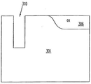
전술된 실시예는 기판의 표면이 기본적으로 평면인 구조를 설명한다. 비 평면 구조(200)는 도 6A에 도시된다. 기판(205)은 상면(202)을 구비한다. 트렌치(201)는 기판(205) 내에 에칭되고, 필드 산화물 영역이 기판 내 하방과 표면(202) 위 상방으로 확장하도록 필드 산화물 영역(203)이 기판에서 열 성장된다. 폴리 실리콘 레이어(204)는 필드 산화물 영역(203)의 상부에 피착 된다. 명백하듯이, 트렌치(201)의 바닥과 폴리 실리콘(204)의 상부 사이에는 상당한 높이 차이가 있다. 트렌치(201)가 유전체로 충전되면, 유전체의 표면을 표면(202)과 평탄하게하는 데 에칭이 사용될 수 있다. 그렇지 않고, CMP가 유전체를 평탄화하는데 사용되면, 필드 산화물 영역(203)의 일부와 함께 폴리실리콘 레이어(204)가 제거될 것이 분명하다.The above described embodiment describes a structure in which the surface of the substrate is basically planar.
이 문제를 해결하는 한가지 방법은 폴리실리콘을 생략하고(또는 프로세스 흐름에서 나중까지 폴리실리콘(204)의 형성을 뒤로 미룸) 표면(202) 아래의 부분이 필요한 전기적 특성을 충분히 제공할 만큼 충분한 두께로 필드 산화물 영역(203)을 성장시키는 것이다. 도 6B는 산화물 레이어(206)로 라이닝되고 BPSG(207)로 충전된 트렌치(201)를 도시하며, 둘 다 트렌치 안으로 에칭되었다. 전체 구조는 질화물 레이어(208)로 커버되고, 이것은 트렌치의 상부 또한 충전한다. 도 6C에서, 상면은 CMP로 평탄화되고 필드 산화물 영역(203)의 바닥부(209)와 BPSG(207) 및 산화물 레이어(206) 위에 보호 질화물 캡(210)을 남긴다. 상면은 전체적으로 평평하다. 비평탄 상면을 가지면 추가 프로세스가 아주 복잡하므로, 도6C에 도시된 평편한 구조가 도 6A에 도시된 구조보다 바람직하다. 또한, 필드 산화물 영역(203)은 열 방식으로 성장되므로, 남은 영역(209)은 매우 폭넓게 될 수 있지만, 트렌치는 매우 좁게 될 수 있다. 요약하면, 도 6C에 도시된 구조는 캡(210) 때문에 에칭에 저항력이 있는 "캡 된" 트렌치와, "캡 안된" 필드 산화물 영역(209)을 포함한다.One way to solve this problem is to omit polysilicon (or postpone the formation of
한편, 도7A-7H는 폭넓은 분리 트렌치와 좁은 분리 트렌치가 최소 단계를 사용하여 형성될 수 있는 프로세스를 도시한다.7A-7H, on the other hand, illustrate a process in which a wide isolation trench and a narrow isolation trench can be formed using minimal steps.
도 7A에서, 하드 마스크 레이어(252)는 기판(251)에 피착되고 포토레지스트 레이어(253)는 하드 마스크 레이어(252)의 상부에 피착된다. 포토레지스트 레이어(253)는 넓은 개구를 형성하도록 에칭되고, 하드 마스크 레이어(252)는 기판(251)의 표면을 노출하는 넓은 개구(254)를 형성하도록 포토레지스트 레이어(253) 내의 넓은 개구를 통해 에칭된다.In FIG. 7A, the
도 7B에 도시된 바와 같이, 기판(251)은 넓은 트렌치(260)를 형성하도록 RIE로 에칭된다. 포토레지스트 레이어(253)는 제거되고, 새로운 포토레지스트 레이어(257)가 피착된다. 트렌치(260)가 너무 깊지 않으면, 포토레지스트 레이어(257)는 트렌치(260)의 바닥과 기판(251)의 상면 사이의 스텝을 커버할 것이다. 비교적 좁은 개구가 포토레지스트 레이어(257)에 에칭되고, 하드 마스크 레이어(252)가 기판(251)의 표면을 노출하는 좁은 개구(256)를 형성하도록 포토레지스트 레이어(257) 내의 개구를 통해 에칭된다. 한편, 레이어(257)는 포토레지스트 레이어(미도시)에 의해 패터닝되고 에칭되는 피착된 하드 마스크 유전체 레이어를 나타낸다.As shown in FIG. 7B, the
도 7C에 도시된 바와 같이, 기판(251)은 좁은 트렌치(261)를 형성하도록 RIE에 의해 에칭된다. 포토레지스트(또는 하드 마스크) 레이어(257)와 하드 마스크 레이어(252)는 그 다음 제거되거나 패터닝 및 에칭된다.As shown in FIG. 7C, the
선택적으로, 희생 산화물 레이어(미도시)가 트렌치(260,261) 내에 성장되고 RIE 프로세스로부터 임의의 결정 손상을 복구하도록 제거된다. 도 7D에 도시된 바와 같이, 얇은 산화물 레이어(262)가 기판(251) 안으로 도펀트의 확산을 막는 배리어로 성장되고, BPSG의 레이어(263)는 구조의 전체 표면 위로 피착 된다. 한편, 후속 프로세싱 단계 동안, 조립 동안, 및 소자 동작 중의 온도 변화 동안, 크래킹을 피하도록 유전체 충전 물질이 충분히 낮은 스트레스를 보이는 한, 레이어(263)는 임의의 도핑되거나 도핑되지 않은 CVD-피착 또는 스피닝된 실리콘 산화물 또는 실리케이트 유리 또는 임의의 다른 유전체 "충전" 물질을 포함할 수 있다.Optionally, a sacrificial oxide layer (not shown) is grown in
물론, 프로세스 시퀀스는 더 좁은 트렌치가 더 넓은 트렌치 전에 형성되도록 수정될 수 있다. Of course, the process sequence can be modified such that narrower trenches are formed before wider trenches.
다음, 도 7E에 도시된 바와 같이, 상기 구조의 전체 상면은 CMP 또는 CMP가 후속되는 짧은 화학적 에칭에 의해 평탄화된다.Next, as shown in FIG. 7E, the entire top surface of the structure is planarized by a short chemical etch followed by CMP or CMP.
선택적으로, 산화물 레이어(262) 및 BPSG 레이어(263)가 도 7F에 도시된 바와 같이 함몰부(270,271)를 형성하도록 트렌치(260,261) 안으로 에칭(예를 들어, 산 또는 드라이 에칭에 의해)된다. 실리콘 이산화물, 실리케이트 유리 또는 BPSG(예를 들어 질화물 또는 폴리이미드)와 유사하지 않은 유전체가 도 7G에 도시된 바와 같이 상기 구조의 상면 위로 피착되고, 상면은 도 7H에 도시된 바와 같이 트렌치(260,261)의 입구에 보호캡(280)을 형성하도록 다시 평탄화된다. 유전체 충전 물질(263)과는 달리, 캡(280)을 형성하기 위해 사용되는 물질은, 물질이 IC 제조시 후속 웨이퍼 프로세싱 동안의 일반 에칭에 의해 침식되지 않고 캡(280)이 크래킹을 피하도록 충분히 얇게 만들어는 한, 깨지기 쉬운 또는 고 스트레스 물질을 포함할 수 있다.Optionally,
도 8A-8J는 캡을 포함하는 분리 트렌치와 캡을 포함하는 필드 산화물 영역을 형성하는 프로세스를 도시한다. 도 8A에 도시한 바와 같이, 패드 산화물 레이어(302)는 실리콘 기판(301) 상에 성장되고, 일반적인 LOCOS 시퀀스에서와 같이, 질화물 레이어(303)가 패드 산화물 레이어(302) 상에 피착 된다. 패드 산화물 레이어는 예를 들어 300-1000Å의 두께가 될 수 있다. 질화물 레이어(303)는 패드 산화물 레이어(302)를 노출하는 폭넓은 개구(304)를 형성하도록 마스크 레이어(미도시)를 통해 에칭된다. 도 8B도시된 바와 같이, 상기 구조체는 개구(304)에 두꺼운 필드 산화물 영역(305)을 형성하도록 가열된다(예를 들어, 900-1100℃에서 1-4 시간 동안). LOCOS 프로세스에서 일반적인 것과 같이, 질화물 레이어(303)는 개구(304)의 에지에서 산화물 확장으로 상승되어 "새 부리" 형상과 유사하게 형성된다. 다음, 질화물 레이어(303)의 남은 부분이 에칭되고(도 8C), 상면이 CMP 프로세스로 평탄화되어, 필드 산화물 레이어(305)의 남은 부분(306)과 패드 산화물 레이어(302) 사이의 전이가 부드러운 도 8D에 도시된 결과를 가져온다.8A-8J illustrate the process of forming a isolation trench comprising a cap and a field oxide region comprising a cap. As shown in FIG. 8A,
다음, 도 8E에 도시된 바와 같이, 포토레지스트 레이어(308)가 좁은 개구(309)를 생성하도록 피착 및 패터닝된다. 산화물 레이어(307)는 도 8F에 도시된 바와 같이 개구(309)를 통해 에칭되고, 기판(301)은 좁은 트렌치(310)를 형성하도록 RIE 프로세스에 의해 에칭되며, 여기서 산화물 레이어(307)는 하드 마스크로 작용한다. 산화물 레이어(307)의 남은 부분은 짧은 세정 단계에서 제거된다.Next, as shown in FIG. 8E,
도 8G에 도시된 바와 같이, 얇은 산화물 레이어(311)가 트렌치(310)의 벽에 성장되고 BPSG 또는 다른 유전체 충전제 레이어(312)가 피착된다. 기판(301)의 상면은 에칭 또는 CMP에 의해 평탄화된다.As shown in FIG. 8G, a
도 8H에 도시된 바와 같이, 트렌치(310) 내의 산화물 레이어(311) 및 BPSG레이어(3l2)와 필드 산화물 영역(305)의 남은 부분(306)은 이들 구성 요소의 상면이 기판의 상면보다 낮아질 때까지 에칭된다. 질화물과 같은 비유사 유전체 레이어(315)가 구조체 위에 피착되고(도 8I), 상기 구조체는 상면을 평탄화하고 트렌치(310)와 필드 산화물(306) 위에 보호캡(316)을 형성하도록(도 8J) 다시 CMP 프로세스를 받게 된다.As shown in FIG. 8H, the
도 9A-9E는 트렌치 분리 구조체 아래가 아닌 필드 산화물 분리 영역 아래에 필드 도핑 영역을 가지는 구조체를 생성하는 프로세스를 도시한다.9A-9E illustrate a process for creating a structure having a field doped region under a field oxide isolation region and not below a trench isolation structure.
도 9AB, 패드 산화물 레이어(351)가 실리콘 기판(350) 상에 성장되고, 질화물 레이어(352)와 포토레지스트 레이어(353)가 패드 산화물 레이어(351)의 상면에 그 순서로 피착된다. 포토레지스트 레이어(353)는 두 개구(354A, 354B)를 형성하도록 패터닝되고, 질화물 레이어(352)는 패드 산화물 레이어(351)를 노출하도록 개구(354A,354B)를 통해 에칭된다. 인(P+)이 N-타입 영역(356A)을 형성하도록 개구(354A,354B)를 통해 주입된다. 인 주입 용량은 일반적으로 5x10¹²~3x1013cm-2의 범위이고, 주입 에너지는 일반적으로 약 80 내지 120keV이다. 한편, 폴리이미드 레이어는 질화물 레이어(352) 대신 치환될 수 있고, 트렌치(374) 에칭을 위한 하드 마스크를 형성하는데 사용될 수 있다.9AB, the
도 9B에 도시된 바와 같이, 포토레지스트 레이어(353)가 제거되고, 새로운 포토레지스트 레이어(355)가 피착되며, 포토레지스트 레이어(353)의 이전 개구(354B)의 위치를 포함하는 개구를 형성하도록 패터닝 된다. P-타입 영역(356B)을 형성하도록 붕소(B+)가 포토레지스트 레이어(355)의 개구를 통해 주입된다. 붕소 주입량은 일반적으로 인 주입량보다 더 크기 때문에 (예를 들면, 8x10¹³~2x1014cm-2), 붕소는 P-타입 영역(356B)을 형성하도록 개구(354B) 아래의 인 영역을 카운터 도핑한다. 붕소 주입 에너지는 일반적으로 60~120keV이다.As shown in FIG. 9B, the
다음, 도 9C에 도시된 바와 같이, 상기 구조체는 개구(354A,354B)의 위치에 두꺼운 필드 산화물 영역(370A,370B)을 형성하도록 가열된다. 필드 산화물 영역(370A,370B)은 두께가 2000Å-2㎛가 될 수 있다(일반적으로 약 0.8㎛). 또한, 이 열처리는 인과 붕소 도펀트를 활성화하고 필드 산화물 영역(370A) 아래에 N-타입 필드 도핑 영역(358A)을 형성하고, 필드 산화물 영역(370B) 아래에 P-타입 필드 도핑 영역(370B)을 형성한다.Next, as shown in FIG. 9C, the structure is heated to form thick field oxide regions 370A, 370B at the locations of the
남은 질화물 레이어(352)는 제거되고(도 9D), 선택적으로 희생 산화가 수행된다. 다음, 도 9E에 도시된 바와 같이, 트렌치(374)는 산화물 레이어(371)를 형성하도록 에칭 및 산화되고, 다음, 위에 설명된 방식으로 BPSG(372)와 같은 물질을 포함하는 유전체로 충전된다. 상기 구조체의 상면은 CMP 또는 에칭으로 평탄화되고, 산화물 레이어(371), BPSG(372) 및 필드 산화물 영역(370A,370B)의 남은 부분이 전술된 방식으로 에칭된다. 질화물(또는 트렌치(374)를 충전하는 데 사용되는 물질과 유사하지 않은 다른 유전체) 레이어가 상면에 피착되고, 그 다음 상면은 보호캡(373)을 형성하도록 평탄화된다.The remaining
이 프로세스는 예를 들어 저전압 장치를 분리하는 데 사용되는 필드 도핑 없는 비교적 좁은 트렌치를 생성하고, 예를 들어 고 전압 CMOS 장치를 분리하는 데 사용되는 필드 도핑된 폭넓은 필드 산화물 영역을 생성한다. 상기 프로세스에 의하면, 설계자는 동일한 반도체 기판에서 상이한 폭과 상이한 필드 도핑을 가진 분리 영역을 형성할 수 있으며, 임의의 추가 프로세싱에 평평한 상면을 제공한다. 또한, 분리 영역에는 원하는 경우, 보호캡이 형성될 수 있다.This process creates a relatively narrow trench without field doping, for example used to isolate low voltage devices, and creates a field doped broad field oxide region, for example used to isolate high voltage CMOS devices. The above process allows the designer to form isolation regions with different widths and different field dopings on the same semiconductor substrate, providing a flat top surface for any further processing. In addition, a protective cap may be formed in the separation region if desired.
일부 실시예에서, 트렌치 내의 물질은 분리된 트렌치 캡 대신에 단계적인 유전체 충전에 의해 보호된다. 그러한 실시예에서, 트렌치는 적어도 부분적으로는 비교적 부드럽고, 저 스트레스의 유전체와 비교적 강하고, 에칭 저항이 큰 유전체의 혼합으로 충전된다. 혼합에서 비교적 강하고 에칭 저항이 큰 유전체의 비율은 트렌치의 입구에 근접할수록 증가한다. 예를 들어, 실리콘 이산화물과 실리콘 질화물의 혼합이 트렌치에 피착되며, 상기 혼합에서 실리콘 질화물의 백분율은 트렌치의 입구에 가까울수록 증가한다.In some embodiments, the material in the trench is protected by stepped dielectric filling instead of a separate trench cap. In such embodiments, the trench is at least partially filled with a mixture of dielectrics of relatively soft, low stress and relatively strong, high etch resistance. The proportion of dielectrics that are relatively strong and have high etch resistance in mixing increases as they approach the inlet of the trench. For example, a mixture of silicon dioxide and silicon nitride is deposited in the trench, in which the percentage of silicon nitride increases as it approaches the inlet of the trench.
본 발명의 특정 실시예가 설명되었지만, 이 실시예는 설명일 뿐 제한하는 것이 아니다. 본 발명의 광범위한 원리에 따른 많은 추가 또는 다른 실시예들이 당업자에게 명백할 것이다.While certain embodiments of the invention have been described, these embodiments are illustrative and not limiting. Many further or other embodiments in accordance with the broad principles of the invention will be apparent to those skilled in the art.
Claims (46)
Applications Claiming Priority (2)
| Application Number | Priority Date | Filing Date | Title |
|---|---|---|---|
| US11/298,075 | 2005-12-09 | ||
| US11/298,075 US20070132056A1 (en) | 2005-12-09 | 2005-12-09 | Isolation structures for semiconductor integrated circuit substrates and methods of forming the same |
Related Child Applications (2)
| Application Number | Title | Priority Date | Filing Date |
|---|---|---|---|
| KR1020117014788A Division KR20110079861A (en) | 2005-12-09 | 2006-12-07 | Separation Structure and Formation Method for Semiconductor Integrated Circuit Board |
| KR1020117014787A Division KR20110081909A (en) | 2005-12-09 | 2006-12-07 | Separation Structure and Formation Method for Semiconductor Integrated Circuit Board |
Publications (1)
| Publication Number | Publication Date |
|---|---|
| KR20080098481A true KR20080098481A (en) | 2008-11-10 |
Family
ID=38138450
Family Applications (4)
| Application Number | Title | Priority Date | Filing Date |
|---|---|---|---|
| KR1020117022767A Expired - Fee Related KR101323497B1 (en) | 2005-12-09 | 2006-12-07 | Isolation structures for semiconductor integrated circuit substrates and methods of forming the same |
| KR1020117014788A Ceased KR20110079861A (en) | 2005-12-09 | 2006-12-07 | Separation Structure and Formation Method for Semiconductor Integrated Circuit Board |
| KR1020117014787A Ceased KR20110081909A (en) | 2005-12-09 | 2006-12-07 | Separation Structure and Formation Method for Semiconductor Integrated Circuit Board |
| KR1020087014965A Ceased KR20080098481A (en) | 2005-12-09 | 2006-12-07 | Separation Structure and Formation Method for Semiconductor Integrated Circuit Board |
Family Applications Before (3)
| Application Number | Title | Priority Date | Filing Date |
|---|---|---|---|
| KR1020117022767A Expired - Fee Related KR101323497B1 (en) | 2005-12-09 | 2006-12-07 | Isolation structures for semiconductor integrated circuit substrates and methods of forming the same |
| KR1020117014788A Ceased KR20110079861A (en) | 2005-12-09 | 2006-12-07 | Separation Structure and Formation Method for Semiconductor Integrated Circuit Board |
| KR1020117014787A Ceased KR20110081909A (en) | 2005-12-09 | 2006-12-07 | Separation Structure and Formation Method for Semiconductor Integrated Circuit Board |
Country Status (7)
| Country | Link |
|---|---|
| US (5) | US20070132056A1 (en) |
| EP (1) | EP1958249A1 (en) |
| JP (4) | JP5438973B2 (en) |
| KR (4) | KR101323497B1 (en) |
| CN (1) | CN101366112B (en) |
| TW (2) | TWI544573B (en) |
| WO (1) | WO2007070311A1 (en) |
Families Citing this family (40)
| Publication number | Priority date | Publication date | Assignee | Title |
|---|---|---|---|---|
| US20080197408A1 (en) * | 2002-08-14 | 2008-08-21 | Advanced Analogic Technologies, Inc. | Isolated quasi-vertical DMOS transistor |
| US7812403B2 (en) * | 2002-08-14 | 2010-10-12 | Advanced Analogic Technologies, Inc. | Isolation structures for integrated circuit devices |
| US7741661B2 (en) * | 2002-08-14 | 2010-06-22 | Advanced Analogic Technologies, Inc. | Isolation and termination structures for semiconductor die |
| US7834421B2 (en) * | 2002-08-14 | 2010-11-16 | Advanced Analogic Technologies, Inc. | Isolated diode |
| US7939420B2 (en) * | 2002-08-14 | 2011-05-10 | Advanced Analogic Technologies, Inc. | Processes for forming isolation structures for integrated circuit devices |
| US7825488B2 (en) * | 2006-05-31 | 2010-11-02 | Advanced Analogic Technologies, Inc. | Isolation structures for integrated circuits and modular methods of forming the same |
| US7667268B2 (en) * | 2002-08-14 | 2010-02-23 | Advanced Analogic Technologies, Inc. | Isolated transistor |
| US7902630B2 (en) * | 2002-08-14 | 2011-03-08 | Advanced Analogic Technologies, Inc. | Isolated bipolar transistor |
| US8089129B2 (en) * | 2002-08-14 | 2012-01-03 | Advanced Analogic Technologies, Inc. | Isolated CMOS transistors |
| US7956391B2 (en) * | 2002-08-14 | 2011-06-07 | Advanced Analogic Technologies, Inc. | Isolated junction field-effect transistor |
| US8513087B2 (en) * | 2002-08-14 | 2013-08-20 | Advanced Analogic Technologies, Incorporated | Processes for forming isolation structures for integrated circuit devices |
| US20070132056A1 (en) * | 2005-12-09 | 2007-06-14 | Advanced Analogic Technologies, Inc. | Isolation structures for semiconductor integrated circuit substrates and methods of forming the same |
| JP2008041895A (en) * | 2006-08-04 | 2008-02-21 | Renesas Technology Corp | Semiconductor device and manufacturing method thereof |
| JP2008041901A (en) * | 2006-08-04 | 2008-02-21 | Toshiba Corp | Semiconductor device and manufacturing method thereof |
| KR100867977B1 (en) | 2006-10-11 | 2008-11-10 | 한국과학기술원 | Tissue perfusion analysis apparatus using indocyanine green blood concentration dynamics and tissue perfusion analysis method using the same |
| US7572712B2 (en) * | 2006-11-21 | 2009-08-11 | Chartered Semiconductor Manufacturing, Ltd. | Method to form selective strained Si using lateral epitaxy |
| US7795681B2 (en) * | 2007-03-28 | 2010-09-14 | Advanced Analogic Technologies, Inc. | Isolated lateral MOSFET in epi-less substrate |
| US7737526B2 (en) * | 2007-03-28 | 2010-06-15 | Advanced Analogic Technologies, Inc. | Isolated trench MOSFET in epi-less semiconductor sustrate |
| US8736016B2 (en) * | 2007-06-07 | 2014-05-27 | Taiwan Semiconductor Manufacturing Company, Ltd. | Strained isolation regions |
| JP2009026829A (en) * | 2007-07-17 | 2009-02-05 | Nec Electronics Corp | Designing method for semiconductor integrated circuit, and mask data generating program |
| JP2009025891A (en) * | 2007-07-17 | 2009-02-05 | Nec Electronics Corp | Semiconductor integrated circuit design method and design program |
| US8067292B2 (en) * | 2008-01-23 | 2011-11-29 | Macronix International Co., Ltd. | Isolation structure, non-volatile memory having the same, and method of fabricating the same |
| US8907405B2 (en) | 2011-04-18 | 2014-12-09 | International Business Machines Corporation | Semiconductor structures with dual trench regions and methods of manufacturing the semiconductor structures |
| US8722479B2 (en) | 2011-05-25 | 2014-05-13 | Globalfoundries Inc. | Method of protecting STI structures from erosion during processing operations |
| US20120326230A1 (en) * | 2011-06-22 | 2012-12-27 | International Business Machines Corporation | Silicon on insulator complementary metal oxide semiconductor with an isolation formed at low temperature |
| KR20130006903A (en) * | 2011-06-27 | 2013-01-18 | 삼성전자주식회사 | Isolation layer structures and methods of forming the same, semiconductor devices having the same, and methods of manufacturing the semiconductor devices |
| US8673738B2 (en) | 2012-06-25 | 2014-03-18 | International Business Machines Corporation | Shallow trench isolation structures |
| US9768055B2 (en) * | 2012-08-21 | 2017-09-19 | Stmicroelectronics, Inc. | Isolation regions for SOI devices |
| US9012300B2 (en) * | 2012-10-01 | 2015-04-21 | United Microelectronics Corp. | Manufacturing method for a shallow trench isolation |
| US9455188B2 (en) * | 2013-01-18 | 2016-09-27 | Globalfoundries Inc. | Through silicon via device having low stress, thin film gaps and methods for forming the same |
| US20140213034A1 (en) * | 2013-01-29 | 2014-07-31 | United Microelectronics Corp. | Method for forming isolation structure |
| US20150069608A1 (en) * | 2013-09-11 | 2015-03-12 | International Business Machines Corporation | Through-silicon via structure and method for improving beol dielectric performance |
| US9076868B1 (en) * | 2014-07-18 | 2015-07-07 | Globalfoundries Inc. | Shallow trench isolation structure with sigma cavity |
| CN105280545A (en) * | 2014-07-24 | 2016-01-27 | 联华电子股份有限公司 | Shallow trench isolation structure of semiconductor device and manufacturing method thereof |
| US9412641B1 (en) | 2015-02-23 | 2016-08-09 | International Business Machines Corporation | FinFET having controlled dielectric region height |
| KR102140358B1 (en) * | 2016-12-23 | 2020-08-03 | 매그나칩 반도체 유한회사 | Integrated semiconductor device having isolation structure for reducing noise |
| CN109216256B (en) | 2017-07-03 | 2021-01-05 | 无锡华润上华科技有限公司 | Trench isolation structure and manufacturing method thereof |
| KR102828453B1 (en) | 2020-06-22 | 2025-07-03 | 삼성전자주식회사 | Variable resistance memory device |
| KR20220094440A (en) | 2020-12-29 | 2022-07-06 | 주식회사 제이디케이바이오 | light cultivating device for adherent diatoms |
| US12575404B2 (en) * | 2023-08-04 | 2026-03-10 | Nanya Technology Corporation | Semiconductor device with protection layer and method for fabricating the same |
Family Cites Families (40)
| Publication number | Priority date | Publication date | Assignee | Title |
|---|---|---|---|---|
| JPS60189237A (en) * | 1984-03-08 | 1985-09-26 | Matsushita Electric Ind Co Ltd | Production of semiconductor device |
| JPS63188952A (en) * | 1987-01-31 | 1988-08-04 | Toshiba Corp | Manufacture of semiconductor device |
| JPH081926B2 (en) * | 1989-03-10 | 1996-01-10 | 日本電気株式会社 | Method for manufacturing isolation groove |
| JP2723598B2 (en) * | 1989-03-20 | 1998-03-09 | 日本電気株式会社 | Method for manufacturing semiconductor device |
| JPH033346A (en) * | 1989-05-31 | 1991-01-09 | Sharp Corp | Manufacture of semiconductor device |
| JPH07111288A (en) * | 1993-10-12 | 1995-04-25 | Matsushita Electric Ind Co Ltd | Method for forming element isolation |
| US5472904A (en) * | 1994-03-02 | 1995-12-05 | Micron Technology, Inc. | Thermal trench isolation |
| JP3365114B2 (en) * | 1994-09-29 | 2003-01-08 | ソニー株式会社 | Method of forming field oxide film in semiconductor device, and method of forming field oxide film and trench isolation region |
| KR0157875B1 (en) * | 1994-11-03 | 1999-02-01 | 문정환 | Manufacturing Method of Semiconductor Device |
| JP2762973B2 (en) * | 1995-11-30 | 1998-06-11 | 日本電気株式会社 | Method for manufacturing semiconductor device |
| KR100226488B1 (en) * | 1996-12-26 | 1999-10-15 | 김영환 | Isolation structure of semiconductor device and manufacturing method thereof |
| JP3058112B2 (en) * | 1997-02-27 | 2000-07-04 | 日本電気株式会社 | Semiconductor device and manufacturing method thereof |
| KR100244272B1 (en) | 1997-04-17 | 2000-03-02 | 김영환 | Method for forming isolation hayer in semiconductor device |
| JP3063705B2 (en) * | 1997-10-14 | 2000-07-12 | 日本電気株式会社 | Method for manufacturing semiconductor device |
| JPH11163118A (en) * | 1997-11-21 | 1999-06-18 | Toshiba Corp | Method for manufacturing semiconductor device |
| US6869858B2 (en) * | 1999-01-25 | 2005-03-22 | Taiwan Semiconductor Manufacturing Company, Ltd. | Shallow trench isolation planarized by wet etchback and chemical mechanical polishing |
| KR100312943B1 (en) * | 1999-03-18 | 2001-11-03 | 김영환 | A semiconductor device and fabricating method thereof |
| KR100290852B1 (en) * | 1999-04-29 | 2001-05-15 | 구자홍 | method for etching |
| US6429149B1 (en) * | 2000-02-23 | 2002-08-06 | International Business Machines Corporation | Low temperature LPCVD PSG/BPSG process |
| KR20020004729A (en) * | 2000-07-07 | 2002-01-16 | 윤종용 | Trench isolation method and structure of that |
| US6406976B1 (en) * | 2000-09-18 | 2002-06-18 | Motorola, Inc. | Semiconductor device and process for forming the same |
| US6406975B1 (en) * | 2000-11-27 | 2002-06-18 | Chartered Semiconductor Manufacturing Inc. | Method for fabricating an air gap shallow trench isolation (STI) structure |
| KR100428806B1 (en) * | 2001-07-03 | 2004-04-28 | 삼성전자주식회사 | Structure of Trench Isolation and Method of Forming The Same |
| JP2003023065A (en) * | 2001-07-09 | 2003-01-24 | Mitsubishi Electric Corp | Element isolation structure of semiconductor device and method of manufacturing the same |
| JP2004055669A (en) * | 2002-07-17 | 2004-02-19 | Fuji Film Microdevices Co Ltd | Solid-state imaging device and manufacturing method thereof |
| KR100460042B1 (en) * | 2002-12-28 | 2004-12-04 | 주식회사 하이닉스반도체 | Method for forming the isolation layer of semiconductor device |
| KR20040059445A (en) * | 2002-12-30 | 2004-07-05 | 주식회사 하이닉스반도체 | Method for forming trench type isolation layer in semiconductor device |
| US7422961B2 (en) * | 2003-03-14 | 2008-09-09 | Advanced Micro Devices, Inc. | Method of forming isolation regions for integrated circuits |
| US6861701B2 (en) * | 2003-03-05 | 2005-03-01 | Advanced Analogic Technologies, Inc. | Trench power MOSFET with planarized gate bus |
| US6869860B2 (en) * | 2003-06-03 | 2005-03-22 | International Business Machines Corporation | Filling high aspect ratio isolation structures with polysilazane based material |
| KR20050014221A (en) * | 2003-07-30 | 2005-02-07 | 주식회사 하이닉스반도체 | A method for manufacturing a field oxide of a semiconductor device |
| US6914015B2 (en) * | 2003-10-31 | 2005-07-05 | International Business Machines Corporation | HDP process for high aspect ratio gap filling |
| KR100532503B1 (en) * | 2004-02-03 | 2005-11-30 | 삼성전자주식회사 | Method for forming shallow trench isolation |
| US7354812B2 (en) * | 2004-09-01 | 2008-04-08 | Micron Technology, Inc. | Multiple-depth STI trenches in integrated circuit fabrication |
| JP2006120953A (en) * | 2004-10-22 | 2006-05-11 | Matsushita Electric Ind Co Ltd | Semiconductor device and manufacturing method thereof |
| US7442621B2 (en) * | 2004-11-22 | 2008-10-28 | Freescale Semiconductor, Inc. | Semiconductor process for forming stress absorbent shallow trench isolation structures |
| JP2006156471A (en) * | 2004-11-25 | 2006-06-15 | Toshiba Corp | Semiconductor device and manufacturing method of semiconductor device |
| US7344942B2 (en) | 2005-01-26 | 2008-03-18 | Micron Technology, Inc. | Isolation regions for semiconductor devices and their formation |
| US7323379B2 (en) * | 2005-02-03 | 2008-01-29 | Mosys, Inc. | Fabrication process for increased capacitance in an embedded DRAM memory |
| US20070132056A1 (en) | 2005-12-09 | 2007-06-14 | Advanced Analogic Technologies, Inc. | Isolation structures for semiconductor integrated circuit substrates and methods of forming the same |
-
2005
- 2005-12-09 US US11/298,075 patent/US20070132056A1/en not_active Abandoned
-
2006
- 2006-12-07 EP EP06844906A patent/EP1958249A1/en not_active Withdrawn
- 2006-12-07 KR KR1020117022767A patent/KR101323497B1/en not_active Expired - Fee Related
- 2006-12-07 KR KR1020117014788A patent/KR20110079861A/en not_active Ceased
- 2006-12-07 KR KR1020117014787A patent/KR20110081909A/en not_active Ceased
- 2006-12-07 CN CN2006800525978A patent/CN101366112B/en not_active Expired - Fee Related
- 2006-12-07 WO PCT/US2006/046579 patent/WO2007070311A1/en not_active Ceased
- 2006-12-07 KR KR1020087014965A patent/KR20080098481A/en not_active Ceased
- 2006-12-07 JP JP2008544483A patent/JP5438973B2/en not_active Expired - Fee Related
- 2006-12-08 TW TW103103967A patent/TWI544573B/en not_active IP Right Cessation
- 2006-12-08 TW TW095146069A patent/TWI460818B/en not_active IP Right Cessation
-
2008
- 2008-04-30 US US12/150,727 patent/US7915137B2/en not_active Expired - Fee Related
- 2008-04-30 US US12/150,609 patent/US7955947B2/en not_active Expired - Fee Related
- 2008-04-30 US US12/150,704 patent/US7923821B2/en not_active Expired - Lifetime
- 2008-04-30 US US12/150,732 patent/US7994605B2/en not_active Expired - Fee Related
-
2013
- 2013-04-02 JP JP2013076644A patent/JP2013168662A/en active Pending
-
2014
- 2014-11-04 JP JP2014224436A patent/JP6026486B2/en not_active Expired - Fee Related
-
2016
- 2016-04-05 JP JP2016075672A patent/JP6263569B2/en not_active Expired - Fee Related
Also Published As
| Publication number | Publication date |
|---|---|
| JP2013168662A (en) | 2013-08-29 |
| JP6263569B2 (en) | 2018-01-17 |
| US20070132056A1 (en) | 2007-06-14 |
| KR20110079861A (en) | 2011-07-08 |
| KR20110081909A (en) | 2011-07-14 |
| US20100055864A1 (en) | 2010-03-04 |
| US7994605B2 (en) | 2011-08-09 |
| JP2016164998A (en) | 2016-09-08 |
| CN101366112B (en) | 2011-05-04 |
| US20080203543A1 (en) | 2008-08-28 |
| KR20110111549A (en) | 2011-10-11 |
| JP2009518867A (en) | 2009-05-07 |
| EP1958249A1 (en) | 2008-08-20 |
| US7915137B2 (en) | 2011-03-29 |
| KR101323497B1 (en) | 2013-10-31 |
| US7923821B2 (en) | 2011-04-12 |
| CN101366112A (en) | 2009-02-11 |
| TW200733297A (en) | 2007-09-01 |
| TW201419444A (en) | 2014-05-16 |
| US20080254592A1 (en) | 2008-10-16 |
| JP5438973B2 (en) | 2014-03-12 |
| TWI460818B (en) | 2014-11-11 |
| JP6026486B2 (en) | 2016-11-16 |
| US7955947B2 (en) | 2011-06-07 |
| WO2007070311A1 (en) | 2007-06-21 |
| TWI544573B (en) | 2016-08-01 |
| US20080203520A1 (en) | 2008-08-28 |
| JP2015062239A (en) | 2015-04-02 |
Similar Documents
| Publication | Publication Date | Title |
|---|---|---|
| KR101323497B1 (en) | Isolation structures for semiconductor integrated circuit substrates and methods of forming the same | |
| KR100510232B1 (en) | How to reduce non-uniformity of refill layer thickness in semiconductor devices | |
| KR100383504B1 (en) | Semiconductor device and method of producing the same | |
| KR100538810B1 (en) | Method of isolation in semiconductor device | |
| US6551901B1 (en) | Method for preventing borderless contact to well leakage | |
| WO1996015552A1 (en) | Forming a planar surface over a substrate by modifying the topography of the substrate | |
| KR20010038607A (en) | A method of field isolation for semiconductor devices | |
| KR100587084B1 (en) | Manufacturing method of semiconductor device | |
| US6396152B2 (en) | Semiconductor device and production method thereof | |
| KR100815962B1 (en) | Manufacturing method of semiconductor device | |
| CN104362138B (en) | Circuit layout structure | |
| KR20050117330A (en) | Method of making isolation layer of semiconductor device | |
| KR20010074392A (en) | Isolation method for semiconductor devices | |
| KR19990003909A (en) | Device Separating Method of Semiconductor Device |
Legal Events
| Date | Code | Title | Description |
|---|---|---|---|
| PA0105 | International application |
St.27 status event code: A-0-1-A10-A15-nap-PA0105 |
|
| T11-X000 | Administrative time limit extension requested |
St.27 status event code: U-3-3-T10-T11-oth-X000 |
|
| P11-X000 | Amendment of application requested |
St.27 status event code: A-2-2-P10-P11-nap-X000 |
|
| P13-X000 | Application amended |
St.27 status event code: A-2-2-P10-P13-nap-X000 |
|
| R18-X000 | Changes to party contact information recorded |
St.27 status event code: A-3-3-R10-R18-oth-X000 |
|
| PG1501 | Laying open of application |
St.27 status event code: A-1-1-Q10-Q12-nap-PG1501 |
|
| A201 | Request for examination | ||
| P11-X000 | Amendment of application requested |
St.27 status event code: A-2-2-P10-P11-nap-X000 |
|
| P13-X000 | Application amended |
St.27 status event code: A-2-2-P10-P13-nap-X000 |
|
| PA0201 | Request for examination |
St.27 status event code: A-1-2-D10-D11-exm-PA0201 |
|
| E902 | Notification of reason for refusal | ||
| PE0902 | Notice of grounds for rejection |
St.27 status event code: A-1-2-D10-D21-exm-PE0902 |
|
| T11-X000 | Administrative time limit extension requested |
St.27 status event code: U-3-3-T10-T11-oth-X000 |
|
| T11-X000 | Administrative time limit extension requested |
St.27 status event code: U-3-3-T10-T11-oth-X000 |
|
| T11-X000 | Administrative time limit extension requested |
St.27 status event code: U-3-3-T10-T11-oth-X000 |
|
| A107 | Divisional application of patent | ||
| E13-X000 | Pre-grant limitation requested |
St.27 status event code: A-2-3-E10-E13-lim-X000 |
|
| P11-X000 | Amendment of application requested |
St.27 status event code: A-2-2-P10-P11-nap-X000 |
|
| P13-X000 | Application amended |
St.27 status event code: A-2-2-P10-P13-nap-X000 |
|
| PA0104 | Divisional application for international application |
St.27 status event code: A-0-1-A10-A17-div-PA0104 St.27 status event code: A-0-1-A10-A16-div-PA0104 |
|
| A107 | Divisional application of patent | ||
| PA0104 | Divisional application for international application |
St.27 status event code: A-0-1-A10-A18-div-PA0104 St.27 status event code: A-0-1-A10-A16-div-PA0104 |
|
| E601 | Decision to refuse application | ||
| PE0601 | Decision on rejection of patent |
St.27 status event code: N-2-6-B10-B15-exm-PE0601 |
|
| T11-X000 | Administrative time limit extension requested |
St.27 status event code: U-3-3-T10-T11-oth-X000 |
|
| P22-X000 | Classification modified |
St.27 status event code: A-2-2-P10-P22-nap-X000 |