KR20070038015A - Semiconductor memory device - Google Patents
Semiconductor memory device Download PDFInfo
- Publication number
- KR20070038015A KR20070038015A KR1020060097245A KR20060097245A KR20070038015A KR 20070038015 A KR20070038015 A KR 20070038015A KR 1020060097245 A KR1020060097245 A KR 1020060097245A KR 20060097245 A KR20060097245 A KR 20060097245A KR 20070038015 A KR20070038015 A KR 20070038015A
- Authority
- KR
- South Korea
- Prior art keywords
- transistor
- memory cell
- potential
- well
- layer
- Prior art date
Links
Images


Classifications
-
- G—PHYSICS
- G11—INFORMATION STORAGE
- G11C—STATIC STORES
- G11C11/00—Digital stores characterised by the use of particular electric or magnetic storage elements; Storage elements therefor
- G11C11/21—Digital stores characterised by the use of particular electric or magnetic storage elements; Storage elements therefor using electric elements
- G11C11/34—Digital stores characterised by the use of particular electric or magnetic storage elements; Storage elements therefor using electric elements using semiconductor devices
- G11C11/40—Digital stores characterised by the use of particular electric or magnetic storage elements; Storage elements therefor using electric elements using semiconductor devices using transistors
- G11C11/41—Digital stores characterised by the use of particular electric or magnetic storage elements; Storage elements therefor using electric elements using semiconductor devices using transistors forming static cells with positive feedback, i.e. cells not needing refreshing or charge regeneration, e.g. bistable multivibrator or Schmitt trigger
- G11C11/412—Digital stores characterised by the use of particular electric or magnetic storage elements; Storage elements therefor using electric elements using semiconductor devices using transistors forming static cells with positive feedback, i.e. cells not needing refreshing or charge regeneration, e.g. bistable multivibrator or Schmitt trigger using field-effect transistors only
-
- G—PHYSICS
- G11—INFORMATION STORAGE
- G11C—STATIC STORES
- G11C11/00—Digital stores characterised by the use of particular electric or magnetic storage elements; Storage elements therefor
- G11C11/21—Digital stores characterised by the use of particular electric or magnetic storage elements; Storage elements therefor using electric elements
- G11C11/34—Digital stores characterised by the use of particular electric or magnetic storage elements; Storage elements therefor using electric elements using semiconductor devices
- G11C11/40—Digital stores characterised by the use of particular electric or magnetic storage elements; Storage elements therefor using electric elements using semiconductor devices using transistors
- G11C11/41—Digital stores characterised by the use of particular electric or magnetic storage elements; Storage elements therefor using electric elements using semiconductor devices using transistors forming static cells with positive feedback, i.e. cells not needing refreshing or charge regeneration, e.g. bistable multivibrator or Schmitt trigger
- G11C11/413—Auxiliary circuits, e.g. for addressing, decoding, driving, writing, sensing, timing or power reduction
- G11C11/417—Auxiliary circuits, e.g. for addressing, decoding, driving, writing, sensing, timing or power reduction for memory cells of the field-effect type
- G11C11/419—Read-write [R-W] circuits
-
- G—PHYSICS
- G11—INFORMATION STORAGE
- G11C—STATIC STORES
- G11C5/00—Details of stores covered by group G11C11/00
- G11C5/02—Disposition of storage elements, e.g. in the form of a matrix array
- G11C5/025—Geometric lay-out considerations of storage- and peripheral-blocks in a semiconductor storage device
-
- G—PHYSICS
- G11—INFORMATION STORAGE
- G11C—STATIC STORES
- G11C5/00—Details of stores covered by group G11C11/00
- G11C5/06—Arrangements for interconnecting storage elements electrically, e.g. by wiring
- G11C5/063—Voltage and signal distribution in integrated semi-conductor memory access lines, e.g. word-line, bit-line, cross-over resistance, propagation delay
Landscapes
- Engineering & Computer Science (AREA)
- Microelectronics & Electronic Packaging (AREA)
- Computer Hardware Design (AREA)
- Semiconductor Memories (AREA)
- Static Random-Access Memory (AREA)
- Thin Film Transistor (AREA)
Abstract
본 발명은, 미세화된 트랜지스터를 사용한 저소비 전력SRAM에 있어서, 드레인 전극으로부터 기판전극에 흐르는 리크 전류 및 서브 스레숄드 리크전류를 저감하는 것에 의해 LSI원로 전체의 소비 전력을 저감하는 동시에, 메모리 셀의 기록·판독시의 동작 안정성을 향상시키는 기술의 제공에 있다.According to the present invention, in a low power consumption SRAM using a miniaturized transistor, the power consumption of the entire LSI source is reduced while the leakage current and subthreshold leakage current flowing from the drain electrode to the substrate electrode are reduced. There is provided a technique for improving the operational stability at the time of reading.
또한, 트랜지스터의 수를 증가 등에 의한 메모리 셀의 증가를 억제하고, 칩 면적의 증대를 억제하는 기술의 제공에 있다.Further, the present invention provides a technique for suppressing an increase in a memory cell due to an increase in the number of transistors and an increase in chip area.
박스층을 구비하는 SOI 또는 FD-SOI 트랜지스터를 사용해서 구성된 SRAM 메모리 셀에 있어서, 구동 트랜지스터의 박스층하의 웰 전위를 제어함으로써 트랜지스터의 문턱치전압을 제어해서 전류를 증가시켜서, 메모리 셀의 안정 동작을 가능하게 한다.In an SRAM memory cell constructed using a SOI or FD-SOI transistor having a box layer, the threshold voltage of the transistor is controlled to increase the current by controlling the well potential under the box layer of the driving transistor, thereby increasing the stable operation of the memory cell. Make it possible.
서브 스레숄드 리크전류, 구동 트랜지스터, 문턱치전압 Sub Threshold Leakage Current, Driving Transistor, Threshold Voltage
Description
도 1은 본 발명이 적용된 SRAM 메모리 셀의 회로구성의 개략도이다.1 is a schematic diagram of a circuit configuration of an SRAM memory cell to which the present invention is applied.
도 2는 본 발명이 적용된 SRAM내의 웰 노드의 전압관계를 나타내는 도면이다.2 is a diagram showing a voltage relationship of a well node in an SRAM to which the present invention is applied.
도 3은 본 발명에서 사용되는 트랜지스터 구조의 단면의 개략도이다.3 is a schematic diagram of a cross section of a transistor structure used in the present invention.
도 4는 본 발명에서 사용되는 트랜지스터의 등가 회로를 나타내는 도면이다.4 is a view showing an equivalent circuit of a transistor used in the present invention.
도 5는 본 발명이 적용된 SRAM 메모리 셀의 레이아웃의 개략도이다.5 is a schematic diagram of a layout of an SRAM memory cell to which the present invention is applied.
도 6은 본 발명이 적용된 SRAM 메모리 셀의 단면도이다.6 is a cross-sectional view of an SRAM memory cell to which the present invention is applied.
도 7은 본 발명이 적용된 SRAM 메모리 셀의 단면도이다.7 is a cross-sectional view of an SRAM memory cell to which the present invention is applied.
도 8은 본 발명이 적용된 SRAM의 웰 노드를 제어하는 회로의 개략도이다.8 is a schematic diagram of a circuit for controlling a well node of an SRAM to which the present invention is applied.
도 9는 본 발명이 적용된 SRAM의 제어 회로의 개략도이다.9 is a schematic diagram of a control circuit of an SRAM to which the present invention is applied.
도 10은 본 발명이 적용된 SRAM의 워드선 드라이버의 개략도이다.10 is a schematic diagram of a word line driver of an SRAM to which the present invention is applied.
도 11은 본 발명이 적용된 SRAM의 워드선 드라이버의 개략도이다.11 is a schematic diagram of a word line driver of an SRAM to which the present invention is applied.
도 12는 본 발명이 적용된 SRAM내의 각 노드의 전위변화를 나타내는 도면이다.12 is a diagram showing the potential change of each node in the SRAM to which the present invention is applied.
도 13은 본 발명이 적용된 SRAM내의 웰 노드의 전압관계를 나타내는 도면이다.13 is a diagram showing a voltage relationship of a well node in an SRAM to which the present invention is applied.
도 14는 본 발명이 적용된 SRAM 메모리 셀의 회로구성의 개략도이다.14 is a schematic diagram of a circuit configuration of an SRAM memory cell to which the present invention is applied.
도 15는 본 발명이 적용된 SRAM내의 각 노드의 전위변화를 나타내는 도면이다.15 is a diagram showing a potential change of each node in the SRAM to which the present invention is applied.
도 16는 본 발명이 적용된 SRAM내의 각 노드의 전위변화를 나타내는 도면이다.Fig. 16 shows the potential change of each node in the SRAM to which the present invention is applied.
도 17은 본 발명이 적용된 SRAM 메모리 셀의 회로구성의 개략도이다.17 is a schematic diagram of a circuit configuration of an SRAM memory cell to which the present invention is applied.
도 18은 본 발명이 적용된 SRAM내의 각 노드의 전위변화를 나타내는 도면이다.18 is a diagram showing a potential change of each node in an SRAM to which the present invention is applied.
도 19는 본 발명이 적용된 SRAM 메모리 셀의 레이아웃의 개략도이다.19 is a schematic diagram of a layout of an SRAM memory cell to which the present invention is applied.
도 20은 본 발명이 적용된 SRAM내의 웰 노드의 전압관계를 나타내는 도면이다.20 is a diagram showing a voltage relationship of a well node in an SRAM to which the present invention is applied.
도 21은 본 발명이 적용된 SRAM의 웰 노드를 제어하는 회로의 개략도이다.21 is a schematic diagram of a circuit for controlling a well node of an SRAM to which the present invention is applied.
도 22는 본 발명이 적용된 SRAM 메모리 셀의 회로구성의 개략도이다.22 is a schematic diagram of a circuit configuration of an SRAM memory cell to which the present invention is applied.
도 23은 본 발명이 적용된 SRAM내의 각 노드의 전위변화를 나타내는 도면이다.Fig. 23 shows the potential change of each node in the SRAM to which the present invention is applied.
도 24는 본 발명이 적용된 SRAM 메모리 셀의 레이아웃의 개략도이다.24 is a schematic diagram of a layout of an SRAM memory cell to which the present invention is applied.
도 25는 본 발명이 적용된 SRAM 메모리 셀의 단면도이다.25 is a cross-sectional view of an SRAM memory cell to which the present invention is applied.
도 26는 본 발명이 적용된 SRAM의 웰 노드를 제어하는 회로의 개략도이다.26 is a schematic diagram of a circuit for controlling a well node of an SRAM to which the present invention is applied.
도 27은 본 발명이 적용된 SRAM내의 각 노드의 전압관계를 나타내는 도면이다.27 is a diagram showing the voltage relationship of each node in the SRAM to which the present invention is applied.
도 28은 본 발명이 적용된 SRAM 내의 웰 노드의 전압관계를 나타내는 도면이다.28 is a diagram illustrating a voltage relationship of a well node in an SRAM to which the present invention is applied.
도 29는 본 발명이 적용된 SRAM 내의 각 노드의 전위변화를 나타내는 도면이다.29 is a diagram showing the potential change of each node in the SRAM to which the present invention is applied.
도 30은 본 발명이 적용된 SRAM 내의 웰 노드의 전압관계를 나타내는 도면이다.30 is a diagram showing a voltage relationship of a well node in an SRAM to which the present invention is applied.
도 31은 막두께와 웰 노드로의 인가전압의 관계를 나타내는 도면이다.Fig. 31 shows the relationship between the film thickness and the voltage applied to the well node.
도 32는 종래의 SRAM 메모리 셀의 회로구성의 개략도이다.32 is a schematic diagram of a circuit configuration of a conventional SRAM memory cell.
도 33은 본 발명이 적용된 SRAM을 탑재하는 시스템 LSI의 개략도이다.Fig. 33 is a schematic diagram of a system LSI equipped with an SRAM to which the present invention is applied.
(부호의 설명)(Explanation of the sign)
TR1,TR2,201,202 전송 트랜지스터TR1, TR2,201,202 transfer transistor
DR1,DR2,203,204 구동 트랜지스터DR1, DR2,203,204 driving transistor
LD1,LD2 205,206 부하 트랜지스터LD1, LD2 205,206 Load Transistors
NT, NB, 207, 208 메모리 셀 내의 데이터 기억 노드Data storage nodes in NT, NB, 207, and 208 memory cells
WL 워드선 Vdd 전원선WL Word Line Vdd Power Line
Vss 접지 전위 LT, BLB, BLT[n],BLB[n],BLT[n+1],BLB[n+1] 비트 선 Vss ground potential LT, BLB, BLT [n], BLB [n], BLT [n + 1], BLB [n + 1] bit lines
VBN, VBN [n], VBN [n+1], VBN1, VBN2, VBN[4n] nMOS 웰 노드VBN, VBN [n], VBN [n + 1], VBN1, VBN2, VBN [4n] nMOS well node
VBN[4n+1], VBN[4n+2], VBN[k], VBN1[n], VBN2[n] nMOS 웰 노드VBN [4n + 1], VBN [4n + 2], VBN [k], VBN1 [n], VBN2 [n] nMOS well nodes
VBP, VBP[n], VBP[n+1], VBP1, VBP2 pMOS 웰 노드VBP, VBP [n], VBP [n + 1], VBP1, VBP2 pMOS Well Nodes
VBP[4n] VBP[4n+1], VBP[4n+2], VBP[k], VBP1[n], VBP2[n] pMOS 웰 노드VBP [4n] VBP [4n + 1], VBP [4n + 2], VBP [k], VBP1 [n], VBP2 [n] pMOS well nodes
1, 11 게이트 전극 2 드레인 전극 1, 11
3 소스 전극 4 , 17, Well 웰3
5, 18 지지기판 6, 16 매립 산화막층5, 18
7, 13 소자분리층 12 콘택트 콘택트7, 13
19 디퓨젼 확산층 14 게이트 절연막 19
15 SOI층 MC 메모리 셀 15 SOI Layer MC Memory Cells
ys, ys[0]∼ys[3] 컬럼 선택 신호 DRv1…웰 노드 드라이버ys, ys [0] to ys [3] column selection signals DRv1... Well node driver
in…입력 신호 WDR…워드선 드라이버in… Input signal WDR.. Word Line Driver
xa, xb…어드레스 디코드 신호 CK…클록 신호xa, xb ... Address decode signal CK... Clock signal
bwen…기록 신호 D…입력 데이터bwen… Recording signal D... Input data
Vssd…웰 노드 드라이버의 Vss선 Vddd…웰 노드 드라이버의 Vdd선Vssd… Vss line Vddd of the well node driver. Vdd line of well node driver
Vbnst,Vbpst 스탠바이용 웰 노드 전위선Well node potential line for Vbnst, Vbpst standby
stby, stbyb 스탠바이상 제어 신호 stby, stbyb standby phase control signal
Vssm 메모리 셀 내 구동 트랜지스터 소스선 Drive Transistor Source Line in Vssm Memory Cell
Vcc Vdd 보다 높은 전위의 전원선Power supply line with potential higher than Vcc Vdd
SOC 시스템LSI의 칩 CPU CPU 코어 SOC systemLSI chip CPU CPU core
CACHE 캐쉬 메모리 RAM 워크 메모리CACHE Cache Memory RAM Work Memory
PERI 시스템LSI중의 CPU 코어 외의 논리회로.Logic circuits other than the CPU core in the PERI system LSI.
본 발명은, 스태틱 메모리(SRAM)회로가 반도체 칩 상에 집적된 반도체집적회로에 관한 것이고, 특히, SRAM집적회로장치의 동작에 필요한 동작 마진을 넓히는 구성에 관한 것이다.BACKGROUND OF THE
최근, 반도체장치, 예컨대 SRAM 회로 등의 반도체장치에 대하여는, 고속화 및 저소비 전력화가 강하게 요청되고 있다.Recently, high speed and low power consumption have been strongly demanded for semiconductor devices such as semiconductor devices such as SRAM circuits.
도 32에 종래의 SRAM 메모리 셀 회로를 나타낸다. 여기에서, BLT 및 BLB은 비트선, WL은 워드선, Vdd는 하이레벨의 전원선, Vss는 접지 전위선, 201 및 202는 메모리 셀에 액세스하기 위한 전송 트랜지스터, 203 및 204는 메모리 셀의 데이터를 유지하기 위해서 기억 노드를 구동하는 구동 트랜지스터, 205 및 206는 메모리 셀 데이터를 유지하기 위해서 전하를 공급하는 부하 트랜지스터, 207 및 208은 기억 노드이다.32 shows a conventional SRAM memory cell circuit. Here, BLT and BLB are bit lines, WL is a word line, Vdd is a high level power supply line, Vss is a ground potential line, 201 and 202 are transfer transistors for accessing a memory cell, and 203 and 204 are data of a memory cell. The driving
SRAM 회로의 소비 전력을 저감하기 위해서는 전원전압을 저하시키는 것이 가장 단순하고 효과가 큰 방법이다.In order to reduce the power consumption of the SRAM circuit, reducing the power supply voltage is the simplest and most effective method.
그러나, 낮은 전원전압에서는 트랜지스터의 동작에 필요한 동작 마진이 저하하고, 동작이 불안정해진다. 이 문제의 해결을 겨냥한 기술로서, 특허문헌1(특개평11-39879호)에서는, SRAM셀을 구성하는 트랜지스터의 기판전위를 제어하고, 기록시의 고속화와 판독시의 소비 전력을 저감하는 기술이 개시된다. 또한, 특허문헌2(특 개 2003-151277호)에서는, 1개의 메모리 셀에 2종류의 Vth를 가질 트랜지스터를 사용하며, 고속·저전압동작을 가능하게 하는 회로기술이 개시된다. 더욱이, 특허문헌3(특개 2003-86713호)에서는, SRAM 메모리 셀을 구성하는 트랜지스터의 게이트 폭을 좌우의 기억 노드에 접속되는 트랜지스터로 비대칭으로 하는 것으로써 동작시의 데이터 파괴를 막아 저전압동작을 가능하게 하는 기술이 개시된다.However, at low power supply voltages, the operating margin required for the operation of the transistors decreases and the operation becomes unstable. As a technique aimed at solving this problem, Patent Document 1 (Japanese Patent Laid-Open No. Hei 11-39879) discloses a technique for controlling the substrate potential of a transistor constituting an SRAM cell, speeding up writing and reducing power consumption during reading. Is initiated. In addition, Patent Document 2 (Japanese Patent Laid-Open No. 2003-151277) discloses a circuit technology that enables high-speed and low-voltage operation by using a transistor having two kinds of Vth in one memory cell. Further, Patent Document 3 (Patent No. 2003-86713) asymmetrics the gate width of a transistor constituting an SRAM memory cell with a transistor connected to left and right memory nodes to prevent data destruction during operation, thereby enabling low voltage operation. The technique for making it is disclosed.
[특허문헌1]특개평11-39879호 공보 [Patent Document 1] Japanese Patent Laid-Open No. 11-39879
[특허문헌2]특개 2003-151277호 공보 [Patent Document 2] Japanese Patent Application Laid-Open No. 2003-151277
[특허문헌3]특개 2003-86713호 공보[Patent Document 3] Japanese Patent Application Laid-Open No. 2003-86713
LSI (Large Scale (in)tegrated circuit:대규모 집적회로)의 저소비 전력화 및 LSI중의 트랜지스터의 미세화에 의해, LSI의 전원전압이 저하된다. 예를 들면, 90nm 프로세스에서는, 전원전압1.2V에서 동작하는 LSI가 제조된다. 전원전압이 하강하면, SRAM 회로에 있어서는 기록 ·판독의 동작시의 동작 안정성이 저하하고, 동작이 어렵게 된다. 메모리 셀을 구성하는 각 트랜지스터의 구동력 즉 전류가 변화되면 기록, 판독의 안정성 및 동작속도의 각 성능이 변화된다.Due to the low power consumption of the large scale (in) integrated circuit (LSI) and the miniaturization of transistors in the LSI, the power supply voltage of the LSI is lowered. For example, in a 90 nm process, an LSI operating at a power supply voltage of 1.2 V is manufactured. When the power supply voltage drops, the operation stability during the write / read operation in the SRAM circuit is lowered and the operation becomes difficult. As the driving force, i.e., current, of each transistor constituting the memory cell is changed, each performance of write and read stability and operation speed is changed.
따라서, 메모리 셀을 구성하는 각 트랜지스터의 성능을 적절하게 제어할 수가 있으면 각각의 성능을 향상할 수가 있다. 또 전원전압을 저하시키면 트랜지스터의 구동 전류가 내려가기 때문에, 회로의 동작속도가 저하한다. 이 동작속도의 저하를 억제하기 위해서는 트랜지스터의 문턱치전압(Vth)을 낮게 해서 전원전압이 저하해도 동작 전류의 저하를 억제하는 방법이 얻어진다.Therefore, if the performance of each transistor constituting the memory cell can be properly controlled, the respective performance can be improved. When the power supply voltage is lowered, the driving current of the transistor is lowered, so that the operation speed of the circuit is lowered. In order to suppress the decrease in the operation speed, a method is provided in which the threshold voltage Vth of the transistor is lowered to suppress the decrease in the operating current even when the power supply voltage decreases.
그러나, 트랜지스터의 Vth를 저하시키면 서브 스레숄드 리크(sub threshold leak)전류로 불리는 off된 트랜지스터의 소스 드레인간을 흐르는 리크 전류가 증가하고, 비동작 상태에서의 소비 전력이 증가한다는 문제가 있다.특허문헌1의 예에서는, SRAM 메모리 셀 중의 적절한 트랜지스터의 기판전위를 제어함으로써 트랜지스터의 성능을 제어하고, 비동작시의 저전력을 실현하는 기술이 개시된다, n채널형 벌크 CMOS트랜지스터의 백 게이트에 소스 전극보다 낮은 전압을 인가하면 트랜지스터의 Vth를 높게 제어하는 것으로써 가능하며, 트랜지스터의 서브 스레숄드 리크를 억제할 수 있다.However, if the Vth of the transistor is lowered, there is a problem that the leakage current flowing between the source drains of the off transistors, called a sub threshold leak current, increases, and power consumption in an inactive state increases. In the example of 1, a technique of controlling the performance of a transistor by controlling the substrate potential of an appropriate transistor in an SRAM memory cell and realizing a low power during non-operation is disclosed. The back gate of an n-channel bulk CMOS transistor is disclosed as a source electrode. When a low voltage is applied, it is possible to control the transistor's Vth high, thereby suppressing the subthreshold leakage of the transistor.
그러나, 제조 프로세스 90nm이하의 미세화된 벌크 CMOS 트랜지스터의 백 게이트를 제어하면, 접합 리크 전류로 불리는 드레인 전극으로부터 기판전극에 흐르는 리크 전류가 증가하고, 서브 스레숄드 리크전류는 저하되어 있지만, 트랜지스터 전체에서 본 리크 전류는 증가하여 회로전체의 소비 전력을 저감할 수 없다는 문제가 있다.However, when the back gate of the refined bulk CMOS transistor of 90 nm or less in the manufacturing process is controlled, the leakage current flowing from the drain electrode called the junction leakage current to the substrate electrode is increased, and the sub-threshold leakage current is lowered. There is a problem that the leakage current increases so that power consumption of the entire circuit cannot be reduced.
특허문헌2의 예에서는, 1개의 메모리 셀을 구성하는 트랜지스터의 수를 증가시키는 동시에 2종류의 Vth를 가질 트랜지스터를 사용하는 것으로써 메모리 셀 내의 트랜지스터의 구동력을 적절하게 설정하고, 메모리 셀의 기록·판독시의 동작 안정성을 향상시키고 있다.In the example of
그러나, 메모리 셀의 소자수가 증가하기 때문에 크게 메모리 셀 면적이 증가해버린다. 메모리 회로는 될 수 있는 한 많은 용량을 탑재해야 한다는 요구가 있기 때문에, 면적이 증가하는 메모리 셀을 사용하는 것은 어렵다는 문제가 있다.However, since the number of elements of the memory cell is increased, the memory cell area is greatly increased. There is a problem that it is difficult to use a memory cell with an increased area because the memory circuit has a requirement to mount as much capacity as possible.
특허문헌3의 예에서는, 원래 대상이어야 할 메모리 셀 내의 트랜지스터의 게이트 폭에 비대칭성을 갖게 하는 것으로써 메모리 셀 내의 트랜지스터의 구동력을 적절하게 설정하고, 이것에 의해 메모리 셀이 가질 기록·판독시의 동작 안정성을 향상시켜 있다.In the example of
그러나, 게이트 폭을 좌우로 변화시키기 위해서 메모리 셀의 대칭성을 상실한다. 메모리 셀을 제조할 때에는, 같은 메모리 셀을 대량으로 반복하여 배치할 수 있다는 규칙성이 높고 대칭적인 메모리 셀을 사용한다는 대칭성이 높아서 정밀도가 높은 메모리 셀을 만들고 있지만, 대칭성이 무너져버리면 이 제조 정밀도가 저하해서, 성능이 저하한다는 문제가 있다. 또한 다른 게이트 폭을 사용하는 는 것은 메모리 셀 면적이 증대한다는 문제도 안고 있어, 이것은 특허문헌2의 예와 같은 면적증가라는 문제에 이른다.However, the symmetry of memory cells is lost to change the gate width from side to side. When manufacturing a memory cell, the memory cell is manufactured with high precision due to the high symmetry that the same memory cell can be repeatedly arranged in large quantities and the symmetrical memory cell is used, but when the symmetry is broken, the manufacturing precision is reduced. There is a problem that the performance decreases. In addition, using a different gate width also has a problem that the memory cell area increases, which leads to a problem of area increase as in the example of
본 발명이 해결하고자 하는 문제는, 미세화된 트랜지스터를 사용한 저소비 전력SRAM에 있어서, 드레인 전극으로부터 기판전극에 흐르는 리크 전류 및 서브 스레숄드 리크전류를 저감하는 것에 의해 LSI 회로전체의 소비 전력을 저감하는 기술을 제공하는 점에 있다.The problem to be solved by the present invention is a technique for reducing the power consumption of the entire LSI circuit by reducing the leakage current and the sub-threshold leakage current flowing from the drain electrode to the substrate electrode in a low power consumption SRAM using a miniaturized transistor. The point is to provide.
또한, 메모리 셀의 기록·판독시의 동작 안정성을 향상시키는 기술의 제공에 있다.Another object of the present invention is to provide a technique for improving the operational stability at the time of writing and reading a memory cell.
더욱이, 트랜지스터의 수를 증가 등에 의한 메모리 셀의 증가를 억제하고, 칩 면적의 증대를 억제하는 기술의 제공에 있다.Furthermore, the present invention is to provide a technique for suppressing an increase in a memory cell due to an increase in the number of transistors and for suppressing an increase in chip area.
[문제를 해결하기 위한 수단][Means to solve the problem]
본 발명의 대표적인 것의 하나의 예를 게시하면, 아래와 같다. 즉, 본 발명의 반도 체기억장치는, 데이터를 기억하는 래치부와, 데이터를 전송하는 전송부를 구비하여 이루어지는 스태틱형의 메모리 셀을 구비하고, 그 래치부 및 전송부는, 채널 부분이 절연막으로 이루어지는 박스층에 의해 기판부분과 절연된 SOI층을 구비하는 트랜지스터를 포함하고, 메모리 셀의 데이터의 기록 동작시와 데이터의 판독 동작시에, 메모리 셀 내의 적어도 하나의 트랜지스터의 문턱치전압을 변화시키는 것을 특징으로 하는 것이다.An example of one representative of the present invention is shown below. That is, the semiconductor memory device of the present invention includes a static memory cell including a latch portion for storing data and a transfer portion for transferring data, and the latch portion and the transfer portion are formed of an insulating film. And a transistor having an SOI layer insulated from the substrate portion by the box layer, wherein the threshold voltage of at least one transistor in the memory cell is varied during a data write operation and a data read operation. It is to be done.
이에 의해서, 스태틱형의 메모리 셀을 SOI 트랜지스터로 구성하고, 각 트랜지스터의 매립 산화막(박스:Buried OXide)층의 아래쪽의 웰층의 전위를 적절하게 제어함으로써 각 트랜지스터의 전류를 변화시켜 SRAM의 각 성능을 향상시키는 것이 가능해진다. 웰층은 박스층에 의해 트랜지스터가 형성되는 SOI층과는 전기적으로 절연되기 때문에 여분인 리크 전류는 증가하지 않는다.As a result, the static memory cells are composed of SOI transistors, and the potential of the well layer under the buried oxide film (box: Burried OXide) layer of each transistor is appropriately controlled to change the current of each transistor to improve the performance of each SRAM. It becomes possible to improve. Since the well layer is electrically insulated from the SOI layer where the transistor is formed by the box layer, the extra leakage current does not increase.
또한, 본 발명의 반도체기억장치는, 반도체기판에 형성된 도전층으로 이루어지는 웰층과, 그 웰층 위로 형성된 절연막으로 이루어지는 박스층과, 박스층위로 형성된 소스층, 드레인층 및 소스층과 드레인층에 끼워져 있어서 형성된 채널층과, 그 채널층 위로 게이트 절연막을 통해서 형성된 게이트 전극을 구비하는 SOI형 트랜지스터를 복수 구비해서 이루어지고, 스태틱형 메모리 셀로서 기능하는 반도체기억장치이며, 접지 전위선에 그 소스 전극이 접속되어, SOI형 트랜지스터로 이루어지는 제1의 도전형 채널을 구비하는 구동 트랜지스터 쌍과, 접지선의 전위보다 높은 전위가 되는 제1의 전원선에 그 소스 전극이 접속되어, 드레인 전극을 통해서 상기 구동 트랜지스터와 접속된 SOI형 트랜지스터로 이루어지는 제2의 도전형 채널을 구 비하는 부하 트랜지스터 쌍과, 메모리 셀에 액세스하기 위한 비트선과 정보를 유지하는 기억 노드의 사이에 접속되며, SOI형 트랜지스터로 이루어지는 제1의 도전형 채널을 구비하는 전송 트랜지스터 쌍을 구비하고, 구동 트랜지스터 쌍의 한쪽이 형성되는 웰층과, 전송 트랜지스터 쌍의 한쪽이 형성되는 웰층이, 공통의 제1웰층 위로 설치되어, 부하 트랜지스터 쌍의 한쪽과, 상기 부하 트랜지스터 쌍의 다른 쪽이 공통인 제2웰층 위로 설치되어, 제1웰층과 제2웰층이 서로 전기적으로 분리되는 것을 특징으로 하는 것이다.Further, the semiconductor memory device of the present invention is sandwiched between a well layer made of a conductive layer formed on a semiconductor substrate, a box layer made of an insulating film formed over the well layer, and a source layer, a drain layer, a source layer and a drain layer formed on the box layer. A semiconductor memory device comprising a plurality of SOI transistors including a formed channel layer and a gate electrode formed on the channel layer through a gate insulating film, and functioning as a static memory cell, the source electrode being connected to a ground potential line. And a source transistor connected to a drive transistor pair having a first conductive channel made of an SOI transistor, and a first power supply line having a potential higher than that of the ground line, and the drive transistor being connected to the drive transistor through a drain electrode. A load track comprising a second conductive channel consisting of connected SOI transistors A pair of transfer transistors connected between a pair of jitters, a bit line for accessing a memory cell, and a storage node for holding information, the first transistor having a first conductivity type channel composed of an SOI-type transistor; The well layer to be formed and the well layer on which one of the transfer transistor pairs are formed are provided on a common first well layer, and one of the load transistor pairs and the other of the load transistor pairs are provided on a common second well layer. And the first well layer and the second well layer are electrically separated from each other.
이것에 의해, 적절하게 웰콘택트를 형성하면, 메모리 셀 면적도 증가하지 않는다.As a result, if the well contact is appropriately formed, the memory cell area also does not increase.
더욱이, 본 발명의 반도체기억장치는, 복수의 트랜지스터로 이루어지는 스태틱형 메모리 셀이 열방향 및 행방향으로 배열되어 이루어지고, 메모리 셀 어레이로서 기능하는 반도체기억장치이며, 메모리 셀에 액세스하기 위한 비트선을 복수 구비하고, 복수의 비트선의 하나에 접속된 복수의 메모리 셀을 구성하는 동일한 열내에 형성된 각각의 트랜지스터가 공통되어 설치되는 제1웰층과, 복수의 비트선의 다른 선에 접속된 복수의 메모리 셀을 구성하는 동일한 열내에 형성된 각각의 트랜지스터가 공통되어 설치된 제2웰층을 구비하고, 제1웰층의 전위가 상기 제2웰층의 전위와 다른 전위로 제어되는 것을 특징으로 하는 것이다.Furthermore, the semiconductor memory device of the present invention is a semiconductor memory device in which a static memory cell composed of a plurality of transistors is arranged in a column direction and a row direction, and functions as a memory cell array, and has a bit line for accessing the memory cell. And a plurality of memory cells connected to different lines of the plurality of bit lines, the first well layer having a plurality of transistors and having a plurality of transistors formed in the same column constituting the plurality of memory cells connected to one of the plurality of bit lines in common; Each transistor formed in the same column constituting the same has a second well layer provided in common, and the potential of the first well layer is controlled to a potential different from that of the second well layer.
이것에 의해, 2종류의 전압의 전원을 메모리내의 특정한 노드에 선택적으로 인가하는 것으로써 트랜지스터의 전류를 변화시켜서 각 성능을 향상시키는 것이 가능해진다.As a result, by selectively applying the power of two kinds of voltages to a specific node in the memory, it is possible to change the current of the transistor to improve each performance.
이하에서, 본 발명을, 도면을 사용해서 상세하게 설명한다.EMBODIMENT OF THE INVENTION Below, this invention is demonstrated in detail using drawing.
<실시예1>Example 1
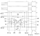
도 1에 본 발명을 사용한 SRAM 회로의 회로도를 나타낸다. 도 1에 있어서, [n]은 n열째로 공통된 것을 나타내고, 동일하게 [n+1]은 n+1열째로 공통된 것을 나타낸다. 이후로, 열(列)에 의해 특별히 구별할 필요가 없을 경우는 []을 빼고 나타내고, 열마다 특징이 있는 점에 관해서는 []을 붙여서 설명을 한다. 도 1에 있어서, BLT 및 BLB은 비트선, WL은 워드선, Vdd는 하이레벨의 전원선, Vss는 접지 전위선, NT 및 NB은 데이터를 기억하는 데이터 유지 노드, TR1 및 TR2은 비트선과 데이터 유지 노드를 접속하는 전송 트랜지스터, DR1 및 DR2은 데이터 유지 노드를 로우레벨로 구동하는 구동 트랜지스터, LD1 및 LD2은 데이터 유지 노드에 전하를 공급하는 부하 트랜지스터, VBN [n]은 n열째의 메모리 셀 내의 nMOS 트랜지스터의 웰 노드가 모두 접속된 노드, VBP[n]은 n열째의 메모리 셀 내의 pMOS 트랜지스터의 웰 노드가 모두 접속된 노드이다. 예를 들면, Vdd는 1.2V, Vss는 0V의 전위가 된다. 본 실시예는, 일반적으로 횡장(橫長) 셀로 불리는 워드선 방향으로 긴 직사각형의 메모리 셀을 사용한 SRAM 회로에 알맞은 회로구성의 예이다. 횡장 셀은, 워드선과 수직방향으로 긴 n웰과 p웰이 교대로 워드선 방향으로 반복해서 나란한 것에 의해 메모리 셀의 형상이 워드선 방향으로 긴 직사각형이 되는 것이다. 그 셀 형상에 기인하여, VBN[k] 및 VBP[k]은, WL에 수직, 즉 비트선에 평행하게 연신하도록 배치된다.The circuit diagram of the SRAM circuit which used this invention in FIG. 1 is shown. In FIG. 1, [n] shows that it is common to nth column, and [n + 1] shows that it is common to n + 1th column similarly. Subsequently, in the case where there is no need to distinguish in particular by the columns, [] is omitted, and the points which are characteristic of each column will be described with []. In Fig. 1, BLT and BLB are bit lines, WL is a word line, Vdd is a high level power supply line, Vss is a ground potential line, NT and NB are data holding nodes for storing data, TR1 and TR2 are bit lines and data. The transfer transistors connecting the sustain nodes, DR1 and DR2, drive transistors for driving the data sustain node to low level, LD1 and LD2 load transistors for supplying charges to the data sustain node, and VBN [n] in the n-th memory cell. A node to which all well nodes of an nMOS transistor are connected, and VBP [n] is a node to which all well nodes of a pMOS transistor in the n-th memory cell are connected. For example, Vdd is 1.2V and Vss is a potential of 0V. This embodiment is an example of a circuit configuration suitable for an SRAM circuit using a rectangular memory cell long in the word line direction generally referred to as a horizontal cell. In a horizontal cell, the shape of a memory cell becomes a rectangle long in a word line direction because n well and p well which are long in a perpendicular direction to a word line alternately repeat in parallel in a word line direction. Due to the cell shape, VBN [k] and VBP [k] are arranged so as to extend perpendicular to WL, that is, parallel to the bit line.
도 1의 회로중에서 사용된 트랜지스터의 단면의 개략도를 도 3에 나타낸다. 여기에서 사용되는 트랜지스터는, 채널 부분이 박스층에 의해 기판부분과 절연되는 SOI 트랜지스터이다. 도 3 중에서, 1은 게이트, 2은 드레인, 3은 소스, 4은 박스층하의 웰층, 5은 지지기판, 6은 매립 산화막(박스)층, 7은 소자분리 영역이다. 본 트랜지스터는 완전공핍형SOI (FD-SOI:Fully Depleted SOI) 트랜지스터 구조가 되어, 웰층의 전위를 제어함으로써, 벌크 CMOS 트랜지스터의 백 게이트 전위를 제어했을 때와 같이 트랜지스터의 Vth를 제어하는 것이 가능하다. 특히 박스층의 두께가 얇으면 얇을수록, 웰층의 전위를 바꾸었을 때의 Vth의 변화도 커진다. 본 발명에서는, 특히 매립 산화막의 막두께가 20nm 이하인 10nm 정도를 상정하고 있다. 그러나, 매립 산화막의 막두께가 20nm 이상인 SOI 트랜지스터에서도, 웰층의 전위를 바꾸었을 때의 Vth의 변화의 정도는 작아지는 것이며, 같은 Vth 제어의 효과를 얻을 수 있다. 또 웰층은, 트랜지스터의 소스 및 드레인등의 확산층과는 절연막인 박스층에 의해 분리되기 때문에, 웰의 전위를 변화시켜도 웰과 확산층간에 전류는 흐르지 않는다.A schematic diagram of a cross section of a transistor used in the circuit of FIG. 1 is shown in FIG. 3. The transistor used here is an SOI transistor whose channel portion is insulated from the substrate portion by a box layer. In FIG. 3, 1 is a gate, 2 is a drain, 3 is a source, 4 is a well layer under a box layer, 5 is a support substrate, 6 is a buried oxide film (box) layer, and 7 is a device isolation region. This transistor has a fully depleted SOI (FD-SOI: Fully Depleted SOI) transistor structure, and by controlling the potential of the well layer, it is possible to control the Vth of the transistor as in the case of controlling the back gate potential of the bulk CMOS transistor. . In particular, the thinner the thickness of the box layer, the larger the change in Vth when the potential of the well layer is changed. In the present invention, the film thickness of the buried oxide film is assumed to be about 10 nm, in particular, 20 nm or less. However, even in an SOI transistor whose film thickness of the buried oxide film is 20 nm or more, the degree of change of Vth when the potential of the well layer is changed becomes small, and the same Vth control effect can be obtained. In addition, since the well layer is separated from the diffusion layers such as the source and the drain of the transistor by a box layer which is an insulating film, current does not flow between the well and the diffusion layer even if the potential of the well is changed.
도 4에서, 도 3의 트랜지스터 구조의 등가 회로를 나타낸다. 1은 게이트, 2은 드레인, 3은 소스, 4은 웰을 나타내고 있으며, 웰과 트랜지스터의 백 게이트는 박스층에 의한 용량에 의해 분리된다. 도 1에서는 이 구조의 트랜지스터가 사용되고 있다.In Fig. 4, an equivalent circuit of the transistor structure of Fig. 3 is shown. 1 represents a gate, 2 represents a drain, 3 represents a source, and 4 represents a well, and the back gate of the well and the transistor is separated by a capacitance by a box layer. In Fig. 1, a transistor of this structure is used.
도 2에서, 각각의 열의 웰 전위의 변화를 나타낸다. VBN [n] 및 VBP[n]은 액세스되는 열의 웰 노드의 전위를 나타내고, VBN [n+1] 및 VBP[n+1]은 액세스되지 않고 있는 열의 웰 노드의 전위를 나타내고 있다. SRAM 에서는 열(列)선택 액세스 가 행하여지는 것이 일반적이기 때문에, 여기에서는 액세스되는 열과 액세스되지 않는 열의 전위를 나타내고 있다. 열선택 액세스가 행하여지지 않고, 모든 열이 액세스될 경우는, 모든 열의 웰 노드의 전위가 VBN [n] 및 VBP[n]에서 나타나 있는 전위와 동일해진다. 판독이 행하여질 경우 및 액세스되지 않고 있을 경우에는 nMOS의 웰 노드 및 pMOS의 웰 노드전위 모두 로우레벨로 제어된다. 또한, 기록이 행하여질 경우에는, nMOS 및 pMOS의 웰 노드의 전위가 하이레벨로 제어된다.In Fig. 2, the change in the well potential of each column is shown. VBN [n] and VBP [n] represent the potentials of the well nodes of the row being accessed, and VBN [n + 1] and VBP [n + 1] represent the potentials of the well nodes of the row not being accessed. In the SRAM, since column selection access is generally performed, the potentials of the columns to be accessed and the columns not to be accessed are shown here. If no column select access is made and all the columns are accessed, the potentials of the well nodes of all the columns become the same as those shown in VBN [n] and VBP [n]. When a read is made and when it is not accessed, both the well node of the nMOS and the well node potential of the pMOS are controlled to low level. In addition, when writing is performed, the potentials of the well nodes of the nMOS and pMOS are controlled to a high level.
도 32의 메모리 셀에 있어서, 기억 노드(207)에 로우의 데이터가, 기억 노드(208)에 하이의 데이터가 기억되어 있을 경우의 판독 동작에 대해서 설명한다. 판독을 할 경우에는, 비트선(BLT 및 BLB)이 하이 전위로 프리챠지된다. 프리챠지 완료후에 워드선(WL)이 하이 전위가 되는 것으로 전송 트랜지스터(201 및 202)이 on이 되고, 하이로 되는 비트선(BLT)의 전하가 전송 트랜지스터(201)로부터 기억 노드(207), 구동 트랜지스터(203)를 통과시켜서 디스챠지되어, (BLT)의 전위가 감지 증폭기에 의해 증폭할 수 있는 레벨이 된 시점에서, 도면에는 나타나지 않고 있지만 비트선에 접속되는 감지 증폭기를 기동하는 것으로써 메모리 셀의 데이터가 증폭되어 출력된다. 여기서 비트선의 전하가 디스챠지되는 경로에 착안하면, 기억 노드(207)는 판독 동작 시작 직전까지는 로우레벨인 0V이지만, 판독 동작이 시작되면 기억 노드(207)는 비트선(BLT)와 (Vss)사이를 전송 트랜지스터(201)와 구동 트랜지스터(203)에 의해 저항 분할한 상태가 되기 때문에, 기억 노드(207)의 전위는 0.3V등 정(正)의 전위가 된다. 여기에서 이 전위가 높아지면, 기억 노드(207)가 게이트에 접속되는 nMOS 트랜지스터의 컨덕턴스가 높아짐과 동시에, 기억 노드(207) 가 게이트에 접속되는 pMOS 트랜지스터의 컨덕턴스가 저하하기 때문에 하이레벨이던 기억 노드(208)의 전위가 저하한다. 더욱이 이 기억 노드(208)의 전위상승은 기억 노드(207)에 피드백되어 이 반복에 의해 메모리 셀에 기억되는 데이터가 파괴된다. 보통 메모리 셀에서는 구동 트랜지스터의 컨덕턴스와 전송 트랜지스터의 컨덕턴스의 비가 1. 5등의 큰 값을 가지도록 설계되어, 메모리 셀에 기억되는 데이터가 파괴될 때까지 기억 노드(207)의 전위가 상승하는 경우는 없다.In the memory cell of FIG. 32, a read operation when a low data is stored in the
그러나, 최근의 트랜지스터 제조 프로세스의 미세화에 의해 트랜지스터 성능의 불균일이 커지는 경향에 있고, 설계시의 컨덕턴스 비(比)를 하회하는 메모리 셀이 제조되어서, 판독시의 동작 안정성이 저하하는 경향이 있다. 또한, 저소비 전력화 때문에 전원전압을 내리면 기억 노드(207)가 게이트에 접속되는 nMOS 트랜지스터 및 pMOS 트랜지스터로 구성되는 인버터의 논리 문턱치전압이 저하하고, 데이터를 파괴하는 피드백이 일어나 쉬워져서, 이것에 의해도 판독시의 동작 안정성이 저하한다.However, recent miniaturization of transistor manufacturing processes tends to increase the variation in transistor performance, and memory cells below the conductance ratio in design tend to be manufactured, resulting in a decrease in the operational stability at the time of reading. In addition, when the power supply voltage is lowered due to lower power consumption, the logic threshold voltage of the inverter composed of the nMOS transistor and the pMOS transistor connected to the
도 1의 본 발명의 회로에 있어서 같이 기억 노드(NT)에 로우의 데이터, 기억 노드(NB)에 하이의 데이터가 기억되어 있을 경우의 판독 동작을 생각하면, 도 32와 거의 같은 동작을 한다. 이 안에서, 부하 트랜지스터((LD1) 및 (LD2))의 웰 전위는 로우전위가 되기 때문에, 종래의 트랜지스터의 상태와 비교하면 (LD1) 및 (LD2)의 Vth가 낮은 상태가 되어, 부하 트랜지스터의 구동력 즉 컨덕턴스는 커지고 있다. 구동 트랜지스터(DR2)의 웰 전위는 소스 전위와 동등하기 때문에, 부하 트랜지스터(LD2)와 구동 트랜지스터(DR2)로 구성되는 인버터의 논리 문턱치전압은, 부하 트 랜지스터(LD2)의 웰 전위가 하이인 상태와 비교하면 높은 상태가 된다. 따라서, 기억 노드(NT)의 전위가 상승했을 경우에도 데이터를 파괴하는 피드백이 일어나기 어려운 상태가 된다.Considering the read operation in the case where the data of the row is stored in the memory node NT and the data of the high in the memory node NB as in the circuit of the present invention of FIG. 1, the operation is almost the same as in FIG. Since the well potentials of the load transistors LD1 and LD2 become low potentials, the Vth of the LD1 and LD2 becomes low compared with the state of the conventional transistor, The driving force, or conductance, is increasing. Since the well potential of the driving transistor DR2 is equal to the source potential, the logic threshold voltage of the inverter composed of the load transistor LD2 and the driving transistor DR2 is such that the well potential of the load transistor LD2 is high. The state becomes high compared with the state. Therefore, even when the potential of the storage node NT rises, the feedback which destroys data hardly occurs.
이렇게, 부하 트랜지스터의 웰 전위가 로우가 되는 상태는 판독시의 동작 안정성이 높다, 즉 판독 동작의 마진이 높은 상태가 되며, 불균일이 적으면서 저전압에서의 동작에 적합하다. 더욱이 본 발명에서는, pMOS 트랜지스터의 웰 전위에 로우의 전위를 인가했을 경우에도 절연막에 의해 웰로부터 확산층에 전류가 흐르지 않기 때문에, 0.5V이상의 PN 접합을 on 시키는 것 같은 높은 전압에서도 소비 전력의 증가 없게 적용하는 것이 가능해진다.Thus, the state in which the well potential of the load transistor becomes low is high in operation stability during reading, that is, in a state in which the margin of the read operation is high, and it is suitable for operation at low voltage with little unevenness. Furthermore, in the present invention, even when a low potential is applied to the well potential of the pMOS transistor, no current flows from the well to the diffusion layer by the insulating film, so that there is no increase in power consumption even at a high voltage such as turning on a PN junction of 0.5 V or more. It becomes possible to apply.
도 32의 메모리 셀에 있어서, 기억 노드(207)에 하이의 데이터가, 기억 노드(208)에 로우의 데이터가 기억되어 있을 경우에 반대의 데이터를 기록할 경우의 동작에 대해서 설명한다. 비트선(BLT)를 로우레벨로, 비트선((BLB))을 하이레벨로 하는 동시에 워드선 전위를” H”레벨로 하고, 전송 트랜지스터를 on 시킨다. 기억 노드(207)의 전하는 전송 트랜지스터(201)를 통과시켜서 디스챠지되어, 기억 노드(207)의 전위는 하이레벨로부터 저하한다. 207의 전위가 부하 트랜지스터(206)와 구동 트랜지스터(204)로 구성되는 인버터의 논리 문턱치보다도 낮아지면, 로우레벨이었던 기억 노드(208)의 전위가 상승하고, 기억 노드간의 피드백도 작용하고, 새로운 데이터가 메모리 셀에 기록된다.In the memory cell of FIG. 32, the operation in the case of writing the opposite data when the high data is stored in the
이렇게 SRAM 메모리 셀에서는 하이레벨의 기억 노드의 전하를 전송 트랜지스터에 의해 디스챠지함으로써 기록이 행하여지지만, 전송 트랜지스터에 의해 전하가 디스챠지됨과 동시에 부하 트랜지스터로부터 전하가 공급되기 때문에, 기록 동작을 끝내기 위해서는, 전송 트랜지스터가 부하 트랜지스터가 공급하는 이상으로 전하를 인출할 필요가 있다. 따라서, 부하 트랜지스터의 컨덕턴스가 커지면 기록에 필요한 시간이 길어지고, 또 불균일 등의 원인에서 설계치를 넘어서 커질 것 같을 경우에는 기록을 할 수 없는 경우가 있다. 이것들을 보상하기 위해서는, 부하 트랜지스터의 컨덕턴스를 작게 하거나, 전송 트랜지스터의 컨덕턴스를 크게 해야 한다.In this way, in the SRAM memory cell, writing is performed by discharging the charge of the high-level memory node by the transfer transistor, but since the charge is discharged by the transfer transistor and the charge is supplied from the load transistor, in order to finish the write operation, It is necessary for the transfer transistor to withdraw the charge beyond that supplied by the load transistor. Therefore, if the conductance of the load transistor is large, the time required for writing becomes long, and if it is likely to increase beyond the design value due to unevenness or the like, there is a case where writing cannot be performed. In order to compensate for these, the conductance of the load transistor must be reduced or the conductance of the transfer transistor must be increased.
lOO321본 실시예에서는, 종래로 같은 동작에서 메모리 셀에 새로운 데이터의 기록이 행하여진다.In the present embodiment, new data is written to the memory cell in the same operation conventionally.
도 1의 회로에서 기록이 행하여지는 열에서는, 부하 트랜지스터((LD1) 및 (LD2))의 웰 전위가 하이로 제어되고, 액세스되지 않고 있을 경우 또는 판독이 행하여질 경우와 비교해서 부하 트랜지스터의 Vth은 상승하고, 구동력은 저하한다. 동시에 메모리 셀중의 nMOS 트랜지스터의 웰 전위가 하이로 제어되어 nMOS 트랜지스터의 Vth는 낮아져 구동력이 높아진다. 따라서, 기록전의 상태에서 하이의 레벨이었던 기억 유지 노드의 전위를 저하시키는 전류를 전송 트랜지스터의 구동력이 높아지는 동시에 하이레벨을 유지하려고 하는 부하 트랜지스터의 구동력이 낮아져, 이에 따라 기록 동작이 행해지기 쉬워진다. 즉 기록시의 동작 마진이 증가하고, 불균일이 적으면서 저전압에서의 동작에 적합하다. 더욱이 본 발명에서는, nMOS 트랜지스터의 웰 전위에 하이의 전위를 인가했을 경우에도 절연막에 의해 웰로부터 확산층으로 전류가 흐르지 않기 때문에 , 0.5V이상의 PN접합을 on 시키는 것 같은 높은 전압에서도 소비 전력의 증가 없이 적용하는 것이 가능해진다.In the column in which writing is performed in the circuit of FIG. 1, the well potentials of the load transistors LD1 and LD2 are controlled high, and the Vth of the load transistor is compared with the case where it is not accessed or when reading is performed. Rises and driving force falls. At the same time, the well potential of the nMOS transistor in the memory cell is controlled to be high, so that the Vth of the nMOS transistor is lowered to increase the driving force. As a result, the driving force of the transfer transistor is increased at the same time that the current of the potential of the storage holding node, which was at the high level in the state before the writing, becomes high, and the driving force of the load transistor which tries to maintain the high level becomes low, thereby making it easy to perform the write operation. That is, the operation margin at the time of recording increases, and it is suitable for operation at low voltage with little unevenness. Furthermore, in the present invention, even when a high potential is applied to the well potential of the nMOS transistor, no current flows from the well to the diffusion layer by the insulating film, so that power consumption does not increase even at a high voltage such as turning on a PN junction of 0.5 V or more. It becomes possible to apply.
이상과 같이, 기록 및 판독의 각각의 동작에서 메모리 셀을 구성하는 트랜지스터의 웰 전위를 적절하게 변화시키는 것으로써 기록 및 판독의 각각의 동작의 동작 마진을 증가시킬 수 있고, 불균일이 적고 저전압에서의 동작에 알맞은 메모리 셀 동작을 할 수 있다.As described above, by appropriately changing the well potential of the transistors constituting the memory cell in each operation of writing and reading, the operation margin of each operation of writing and reading can be increased, and there is less unevenness, and A memory cell operation suitable for the operation can be performed.
도 5에 본 메모리 셀의 레이아웃도를 나타낸다. 도 5에 있어서, TR1 및 TR2은 전송 트랜지스터, DR1 및 DR2은 구동 트랜지스터, LD1 및 LD2은 부하 트랜지스터, 게이트(Gate)는 트랜지스터의 게이트 전극을 구성하는 폴리 실리콘층, 디퓨젼(Diffusion)은 확산층, 콘택트(Contact)는 확산층 및 폴리 실리콘층과 메탈 배선을 접속하기 위한 콘택트, 웰(Well)이 트랜지스터의 웰층이며, 점선에서 둘러싸여진 범위가 1개의 메모리 셀이다. 도 5 중에는 동일한 열(列)인 3개의 메모리 셀이 그려져 있다. 동일한 열로 나란히 서는 메모리 셀의 nMOS 및 pMOS 트랜지스터의 웰층이 접속되어, 동일한 전위로 제어되는 것을 알 수 있다. 또한 더욱이 이웃한 열의 트랜지스터와는 웰층이 분리되어 별개의 전위로 제어되는 것을 알 수 있다. 이 메모리 셀은, 일반적으로 횡장 셀로 불리는 워드선 방향으로 긴 직사각형의 형상을 가질 메모리 셀이다. 횡장 셀은, 워드선과 수직방향으로 긴 n웰과 p웰이 교대로 워드선 방향으로 반복해서 나란한 것에 의해 메모리 셀의 형상이 워드선 방향으로 긴 직사각형이 되는 것이다. 이 셀 형상에 기인하고, 횡장 셀의 SRAM 회로도는 도 1에 도시한 바와 같이 VBN[k] 및 VBP[k]이 워드선(WL)에 수직, 즉 비트선에 평행하게 연신하는 구성이 된다.5 shows a layout diagram of the memory cell. 5, TR1 and TR2 are transfer transistors, DR1 and DR2 are drive transistors, LD1 and LD2 are load transistors, gate is a polysilicon layer constituting a gate electrode of the transistor, diffusion is a diffusion layer, A contact is a contact for connecting a diffusion layer, a polysilicon layer, and a metal wiring, and a well is a well layer of a transistor, and one memory cell is surrounded by a dotted line. In Fig. 5, three memory cells in the same column are drawn. It can be seen that the well layers of the nMOS and pMOS transistors of the memory cells are connected side by side in the same column and controlled at the same potential. Furthermore, it can be seen that the well layer is separated from the transistors in adjacent columns and controlled by a separate potential. This memory cell is a memory cell having a rectangular shape which is generally long in the word line direction called a horizontal cell. In a horizontal cell, the shape of a memory cell becomes a rectangle long in a word line direction because n well and p well which are long in a perpendicular direction to a word line alternately repeat in parallel in a word line direction. Due to this cell shape, the SRAM circuit diagram of the horizontal cell has a configuration in which VBN [k] and VBP [k] are stretched perpendicular to the word line WL, that is, parallel to the bit line, as shown in FIG.
도 6에 도 5중의 A-A'로 절단했을 경우의 단면의 개략을 나타낸다. 도 6에 있어서, 11은 게이트 전극, 12은 콘택트, 13은 소자분리층, 14은 게이트 절연막층, 15은 SOI층, 16은 박스막, 17은 웰층, 18은 지지기판이다. 채널이 형성되는 SOI층은 매립 산화막에 의해 웰층으로부터 절연된다. 이것에 의해, 웰층에 벌크 CMOS 트랜지스터에서의 순방향 바이어스가 인가되어도 웰로부터 소스 전극에 전류가 흐르는 경우는 없다. 또한, 소자분리층에 의해, SOI층 및 웰층은 이웃의 트랜지스터와는 분리된다.6, the outline of the cross section at the time of cut | disconnecting with A-A 'in FIG. 5 is shown. In Fig. 6, 11 is a gate electrode, 12 is a contact, 13 is an isolation layer, 14 is a gate insulating film layer, 15 is an SOI layer, 16 is a box film, 17 is a well layer, and 18 is a support substrate. The SOI layer in which the channel is formed is insulated from the well layer by a buried oxide film. As a result, no current flows from the well to the source electrode even when a forward bias in the bulk CMOS transistor is applied to the well layer. In addition, the device isolation layer separates the SOI layer and the well layer from neighboring transistors.
도 7에 도 5중의 B-B'로 절단했을 경우의 단면의 개략을 나타낸다. 도 7에 있어서, 11은 게이트 전극, 12은 콘택트, 13은 소자분리층, 15은 SOI층, 16은 박스막, 17은 웰층, 18은 지지기판, 19는 확산층이다. 동일한 열 상에 나란히 서는 트랜지스터의 웰이 접속되어서 동 전위로 제어되는 구조가 되는 것을 알 수 있다.The outline of the cross section at the time of cutting | disconnecting with BB 'of FIG. 5 at FIG. In Fig. 7, 11 is a gate electrode, 12 is a contact, 13 is an isolation layer, 15 is an SOI layer, 16 is a box film, 17 is a well layer, 18 is a support substrate, and 19 is a diffusion layer. It can be seen that wells of transistors are connected side by side on the same column, so that the structure is controlled at the same potential.
도 8에 도 2에 기재한 웰 전위의 제어를 하기 위한 회로도를 나타낸다. 도 8에 있어서, VBN[4n]로부터 VBN[4n+2]은 각각의 열의 nMOS 트랜지스터의 웰 전극, VBP[4n]로부터 VBP[4n+2]은 각각의 열의 pMOS 트랜지스터의 웰 전극, DRV1은 웰 전위를 구동하는 구동 회로, ys [0]로부터 ys [3]은 열을 선택하기 위한 열선택 신호, bwen[n]은 그 컬럼에 기록이 행하여지는 것을 나타내는 기록 신호이다. 열선택 신호 및 기록 신호에 의해 선택된 열에 기록이 행하여지고, 도 8의 회로에서는 각각의 신호의 논리곱이 웰 노드에 입력되어, 기록이 행하여질 경우에는 nMOS 및 pMOS의 웰 전위가 하이에, 기록이 행하여지지 않을 경우에는, nMOS 및 pMOS의 웰 전위가 로우로 제어되어, 도 2에 기재한 전위제어가 가능해진다.8 is a circuit diagram for controlling the well potential shown in FIG. 2. In Fig. 8, VBN [4n] to VBN [4n + 2] are well electrodes of nMOS transistors in each column, VBP [4n] to VBP [4n + 2] are well electrodes of pMOS transistors in each column, and DRV1 is well. A driving circuit for driving the potential, ys [0] to ys [3], is a column selection signal for selecting a column, and bwen [n] is a recording signal indicating that writing is performed to the column. Recording is performed in the column selected by the column selection signal and the recording signal. In the circuit of FIG. 8, the logical product of each signal is input to the well node, and when the recording is performed, the well potentials of the nMOS and pMOS are high and the recording is performed. If not performed, the well potentials of the nMOS and pMOS are controlled low, and the potential control shown in Fig. 2 becomes possible.
도 9에 웰 노드를 구동하는 회로(DRV1)의 최종단의 인버터 회로의 하나의 예 를 나타낸다. 도 9에 있어서, Vdd 및 Vss는 전원 노드, (in)은 입력 신호, Vbn은 본인버터 회로의 출력을 나타내고 있다. 본 실시예에 있어서 해당하는 열이 선택되지 않고 있을 경우에는, (in)에 하이의 전위가 인가되어 있고, 해당하는 열에 기록이 행하여질 경우에 (in)의 전위가 로우가 된다. 이것에 의해, 출력(Vbn)은 하이가 되고, 기록 특성을 향상시킨다. 도 9의 회로중의 pMOS 트랜지스터의 웰 노드는 게이트와 접속되어, (in)의 전위가 하이로부터 로우로 변화되면 pMOS 트랜지스터의 웰 노드전위가 로우가 되어서 Vth가 저하해서 구동력이 향상하고, 구동하는 메모리 셀 열의 웰 노드의 전위를 민첩하게 하이로 변화시키는 것이 가능해진다.9 shows an example of an inverter circuit at the final stage of the circuit DRV1 for driving the well node. In Fig. 9, Vdd and Vss denote power nodes, (in) denote input signals, and Vbn denote outputs of magnetic butter circuits. In the present embodiment, when a corresponding column is not selected, a high potential is applied to (in), and a potential of (in) is low when recording is performed in the corresponding column. As a result, the output Vbn becomes high, thereby improving the recording characteristics. The well node of the pMOS transistor in the circuit of FIG. 9 is connected to the gate, and when the potential of (in) changes from high to low, the well node potential of the pMOS transistor becomes low, Vth decreases, and driving force is improved. It is possible to quickly change the potential of the well node of the memory cell row to high.
또한, nMOS트랜지스터의 웰 노드도 게이트 전극과 접속되고 있으며, 해당 메모리 셀 열의 웰 전위를 민첩하게 로우전위로 변화시키는 것이 가능해진다. 동작속도가 중요하지 않을 경우에는, 각각의 웰 전위를 소스 전위에 접속하는 것도 가능하다. 또한, 서브 스레숄드 리크전류가 문제가 안될 경우에는, nMOS 트랜지스터의 웰을 Vdd에, pMOS 트랜지스터의 웰을 Vss에 접속해서 항상 각각의 트랜지스터의 Vth를 낮은 상태로서 두어 동작속도를 향상시킬 수도 있다. 또한, 출력 즉 메모리 셀 내의 웰 노드를 하이로 하는 속도만이 중요해서, 로우로 하는 속도는 느려도 좋을 경우에는, pMOS의 웰 노드뿐 게이트 전극이나 Vss에 접속해서 고속화를 실현하는 것도 가능하다.In addition, the well node of the nMOS transistor is also connected to the gate electrode, and it is possible to change the well potential of the memory cell column to the low potential quickly. When the operation speed is not important, it is also possible to connect each well potential to the source potential. When the sub-threshold leakage current is not a problem, the operation speed can be improved by always connecting the well of the nMOS transistor to Vdd and the well of the pMOS transistor to Vss so that the Vth of each transistor is always kept low. In addition, only the speed of bringing the well node in the output, ie, the memory cell high, is important. When the speed of making the low node may be low, it is possible to realize high speed by connecting only the well node of the pMOS to the gate electrode or Vss.
도 10에 본 SRAM 회로의 워드선을 제어하는 회로의 하나의 예를 나타낸다. 도 10에 있어서, MC은 메모리 셀, WL은 워드선, WDR는 워드선 드라이버, xa 및 xb은 어드레스를 디코드한 신호를 나타낸다. 본 회로구성에서는, xa 및 xb에서 선택 된 1개의 워드선이 워드 드라이버 회로에 의해 하이가 되고, 메모리 셀에 액세스된다.10 shows an example of a circuit for controlling the word lines of the present SRAM circuit. In Fig. 10, MC denotes a memory cell, WL denotes a word line, WDR denotes a word line driver, and xa and xb denote signals that decode an address. In this circuit configuration, one word line selected from xa and xb is made high by the word driver circuit to access the memory cell.
도 11에 도 10 중의 워드 드라이버 회로의 하나의 예를 나타낸다. 이 회로는 xa 및 xb이 입력되는 NAND회로와, 그 출력의 반전 신호를 워드선 전위로서 출력하는 인버터 회로로 구성되어, xa 및 xb의 쌍방이 하이가 되었을 경우에 워드선 전위를 하이로 한다. 보통, 메모리 셀의 동작속도는 워드선의 상승시간에 크게 영향을 받는다. 따라서, 워드선을 로우로부터 하이로 하는 경로를 빨리 하면 크게 메모리의 동작속도를 향상할 수 있다. 본 회로에서는, NAND회로중의 nMOS 트랜지스터와 인버터 회로중의 pMOS 트랜지스터의 웰 노드가 각각 게이트 전극에 접속된다. 따라서, 각각의 트랜지스터는 on이 될 때에 Vth가 저하하고, 구동력이 증가해 동작속도가 커진다. 워드선 전위가 로우로부터 하이가 될 경우에는, NAND회로 중의 nMOS 트랜지스터가 모두 on 하고, 더욱이 인버터 회로의 pMOS 트랜지스터가 on 할 경우이기 때문에, 이렇게 웰 노드와 게이트 노드를 접속하는 것으로써 워드선 전위를 변화시키는 속도가 향상하고, 메모리 전체의 고속화에 기여한다. 또한, 동작속도의 향상이 중요하지 않을 경우에는, 각각의 웰 전위를 소스 전위에 접속하는 것도 가능하다. 또한, 서브 스레숄드 리크전류가 문제가 안될 경우에는, nMOS 트랜지스터의 웰을 Vdd에, pMOS 트랜지스터의 웰을 Vss에 접속해서 항상 각각의 트랜지스터의 Vth를 낮은 상태로서 두어 동작속도를 향상시킬 수도 있다.11 shows an example of the word driver circuit in FIG. This circuit is composed of a NAND circuit into which xa and xb are input, and an inverter circuit which outputs an inverted signal of its output as a word line potential. The word line potential is made high when both of xa and xb become high. Usually, the operating speed of a memory cell is greatly influenced by the rise time of the word line. Therefore, if the path for bringing the word line from low to high is fast, the operation speed of the memory can be greatly improved. In this circuit, well nodes of an nMOS transistor in a NAND circuit and a pMOS transistor in an inverter circuit are connected to a gate electrode, respectively. Therefore, when each transistor is turned on, Vth decreases, driving force increases, and the operation speed increases. When the word line potential goes from low to high, since all the nMOS transistors in the NAND circuit are turned on and the pMOS transistors in the inverter circuit are turned on, the word line potential is connected by connecting the well node and the gate node. The speed of change is improved, which contributes to speeding up the entire memory. In addition, when the improvement of the operation speed is not important, it is also possible to connect each well potential to the source potential. When the sub-threshold leakage current is not a problem, the operation speed can be improved by always connecting the well of the nMOS transistor to Vdd and the well of the pMOS transistor to Vss so that the Vth of each transistor is always kept low.
도 12에 본 실시예의 회로를 사용했을 경우의 회로 각 부분의 동작 전압의 변화를 나타낸다. 도 12 중에서, CK은 클록 신호, WL은 워드선, BLT 및 BLB은 비트 선, VBN 및 VBP은 액세스되는 메모리 셀 내의 트랜지스터의 웰 노드, NT 및 NB은 액세스되는 메모리 셀 내의 기억 유지 노드이며, 기록(Write) 및 판독)Read가 기록 및 판독 동작을 나타낸다. 기록시에는, 클록 신호의 상승과 함께 메모리 셀에 기록되는 데이터가 비트선 상에 입력된다. 또한, 거의 동시에 웰의 전위가 기록 동작에 알맞은 전위로 제어된다. 여기에서, 워드선 전위가 로우로부터 하이로 상승하고, 메모리 셀 내의 기억 노드 전위가 반전하고, 새로운 데이터가 메모리 셀에 기록된다. 판독시에는 클록 신호의 상승에 의해 워드선 전위가 하이가 된다. 이것에 의해 데이터 유지 노드의 데이터가 비트선에 출력되어서 판독이 행하여진다.Fig. 12 shows the change in the operating voltage of each part of the circuit when the circuit of this embodiment is used. In Fig. 12, CK is a clock signal, WL is a word line, BLT and BLB are bit lines, VBN and VBP are well nodes of transistors in a memory cell being accessed, NT and NB are storage holding nodes in a memory cell being accessed. Read and Read indicate write and read operations. At the time of writing, the data written to the memory cell with the rise of the clock signal is input on the bit line. Also, at the same time, the potential of the well is controlled to a potential suitable for the write operation. Here, the word line potential rises from low to high, the memory node potential in the memory cell is reversed, and new data is written to the memory cell. In reading, the word line potential becomes high due to the rise of the clock signal. As a result, the data of the data holding node is output to the bit line and read is performed.
도 33에, 본 발명의 SRAM 메모리를 사용한 SoC(System-on-a Chip)의 예를 나타낸다. SoC은, CPU 코어인 CPU와 그 밖의 특정한 기능을 가진 회로 블록(PERI), 및 여러가지의 회로로부터 액세스되는 비교적 대용량의 메모리RAM으로 구성된다. 또 CPU 코어의 중에는, 캐쉬 메모리(CACHE)가 탑재된다. 본 발명의 SRAM 메모리는, SoC중의 대용량 메모리 및 캐쉬 메모리로서 사용하는 것이 가능하다.33 shows an example of a system-on-a chip (SoC) using the SRAM memory of the present invention. An SoC is composed of a CPU core, a CPU core, a circuit block (PERI) having other specific functions, and a relatively large memory RAM accessed from various circuits. The cache memory CACHE is mounted in the CPU core. The SRAM memory of the present invention can be used as a large memory and a cache memory in an SoC.
<실시예2>Example 2
도 13에 본 발명을 사용한 SRAM 메모리셀 웰전위의 제어 방법의 하나의 예를 나타낸다. 또 이후의 실시예에 있어서, 제1의 실시예와 같은 것에 관해서는 동일한 기호를 사용하고, 다른 것에 관해서만 설명한다. 본 메모리 셀의 트랜지스터 레벨의 회로구성은 도 1과 동등한 회로가 된다. 도 13 중에서, 도 2의 웰 상태와 다른 것은, 메모리에 액세스의 없는 노 액세스(NO access)의 상태에서, pMOS의 웰 전위가 하이레벨이 되는 것이다. 액세스되지 않고 있는 상태, 특히 스탠바이 상태라고 하는 메모리 셀이 데이터는 유지하고 있지만 액세스는 되지 않는 상태에서는, 메모리 셀의 리크 전류가 문제가 될 경우가 있다.13 shows an example of a method of controlling the SRAM memory cell well potential using the present invention. In the following embodiments, the same symbols as those in the first embodiment will be used, and only different ones will be described. The transistor level circuit configuration of this memory cell is equivalent to that of FIG. In FIG. 13, the well state of FIG. 2 is different from the well state of FIG. 2 in that the well potential of the pMOS becomes high in the state of no access without access to the memory. In a state in which the memory cell, which is not accessed, particularly the standby state, retains data but is not accessed, the leak current of the memory cell may be a problem.
이 경우에, pMOS의 웰 전위가 로우가 되면 pMOS의 Vth가 내려 간 상태가 되고, 큰 리크 전류가 흐른다. 도 13의 상태에서는 pMOS의 웰 전위가 하이가 되고, pMOS 의 Vth가 저하하지 않고 리크 전류를 낮게 억제할 수 있다.In this case, when the well potential of the pMOS is low, the Vth of the pMOS is lowered, and a large leak current flows. In the state shown in FIG. 13, the well potential of the pMOS becomes high, and the leak current can be kept low without decreasing the Vth of the pMOS.
<실시예3>Example 3
도 14에 본 발명을 사용한 SRAM 회로의 회로도를 나타낸다. 본 실시예에서는, 실시예1과 달리, 메모리 셀 내의 nMOS 트랜지스터의 웰 노드가, 메모리 셀 내의 좌측 즉 비트선(BLT)로부터 (VSS)까지 직렬로 접속되는 nMOS와, 메모리 셀 내의 오른쪽 즉 비트선((BLB))으로부터 (VSS)까지 직렬로 접속되는 nMOS로 별개의 노드((VBM)과 (VBN2))가 되는 것이다. 메모리 셀의 레이아웃은 도 5로 같지만 이미 좌우의 nMOS의 웰 노드는 별개로 접속되기 때문에 메모리 셀의 레이아웃을 변경할 필요는 없다.Fig. 14 shows a circuit diagram of an SRAM circuit using the present invention. In the present embodiment, unlike the first embodiment, the well node of the nMOS transistor in the memory cell is connected to the left side of the memory cell, that is, the nMOS connected in series from the bit line BLT to the VSS, and the right side of the memory cell, that is, the bit line. NMOSs connected in series from (BLB) to (VSS) become separate nodes ((VBM) and (VBN2)). The layout of the memory cells is the same as in Fig. 5, but since the well nodes of the left and right nMOS are connected separately, there is no need to change the layout of the memory cells.
도 15에 본 실시예의 회로를 사용했을 경우의 회로 각부의 동작 파형을 나타낸다. 실시예1과 다른 것은, 기록시에 (VBN1)과 (VBN2)이 각각인 전위로 제어되는 것이다. 도 15 중에서, 기록시에 (VBN1)은 로우전위인 채이며, (VBN2)은 하이 전위로 제어된다. 이것은, 기록 데이터가 입력되는 비트선 전위와 관계가 있고, (BLT)에 하이의 데이터가, (BLB)에 로우의 데이터가 입력되어 있을 경우는, 도 15의 전위관계가 되어 (VBN1)은 로우전위로, (VBN2)은 하이 전위로 제어된다. 여기서 SRAM 메모리 셀에 데이터를 기록할 때의 동작을 생각한다. 실시예1의 설명에서 쓴 대로, SRAM에 데이터를 기록하는 동작은 하이의 데이터를 유지하고 있는 기억 유지 노드의 전위를, 전송 트랜지스터를 통과시켜서 전류를 흘려서 로우전위로 함으로써 실현된다. (BLB)에 로우의 데이터가 입력되었을 경우에는, 전송 트랜지스터(TR2)를 통과시켜서 큰 전류를 흘릴 수 있으면 기록 특성을 개선할 수 있다. 여기에서, TR2의 웰 노드는 (VBN2)이며, 따라서 (VBN2)의 전위를 하이로 제어하면, 전송 트랜지스터(TR2)의 구동력을 높여서 기록 특성이 개선한다. 여기에서는 도시하지 않고 있지만, (BLT) 에 로우의 데이터가 입력되었을 경우에는 당연히 (VBN1)이 하이로 제어되어서 기록 특성이 개선된다.Fig. 15 shows the operation waveforms of the circuit portions in the case where the circuit of this embodiment is used. The difference from Example 1 is controlled at the potential at which (VBN1) and (VBN2) are respectively at the time of recording. In Fig. 15, (VBN1) remains at low potential during recording, and (VBN2) is controlled at high potential. This is related to the bit line potential to which the write data is input, and when the high data is input to (BLT) and the low data is input to (BLB), this is the potential relationship of FIG. 15, and (VBN1) is low. At the potential, (VBN2) is controlled at the high potential. Here, the operation when writing data to the SRAM memory cell is considered. As described in the description of the first embodiment, the operation of writing data to the SRAM is realized by passing the electric potential of the memory holding node holding the high data through the transfer transistor to the low potential. When low data is input to the BLB, the write characteristics can be improved as long as a large current can flow through the transfer transistor TR2. Here, the well node of TR2 is (VBN2). Therefore, when the potential of (VBN2) is controlled high, the driving force of the transfer transistor TR2 is increased to improve the write characteristics. Although not shown here, when the data of the row is input to (BLT), of course, (VBN1) is controlled high, and the recording characteristic is improved.
도 16에, 도 15의 파형을 실현하기 위한 제어 회로의 회로도를 나타낸다. D는 기록하기 위해서 입력된 데이터 신호이다. D의 값이 비트선(BLT 및 BLB)에 입력되는 동시에, 웰 전위(VBN1)과 (VBN2)이 각각인 전위로 제어할 수 있는 것을 알 수 있다. 이 구성을 취하면, 제어되는 웰이 감소하기 때문에 충방전되는 전하의 양이 감소하고, 기록시의 동작 특성을 동등 레벨로 유지한 채, 소비 전력을 저감하는 것이 가능해진다.FIG. 16 shows a circuit diagram of a control circuit for realizing the waveform of FIG. 15. D is the data signal input for recording. It can be seen that the value of D is input to the bit lines BLT and BLB and can be controlled to the potential at which the well potentials VBN1 and VBN2 are respectively. With this configuration, since the wells to be controlled are reduced, the amount of charge and discharge is reduced, and power consumption can be reduced while maintaining the operation characteristics at the time of writing.
<실시예4>Example 4
도 17에 본 발명을 사용한 SRAM 회로의 회로도를 나타낸다. 본 실시예에서는, 실시예3로부터 더욱이 메모리 셀 내의 좌우의 pMOS의 웰 노드의 제어도 별개로 분할한 구성이다.17 shows a circuit diagram of an SRAM circuit using the present invention. In the present embodiment, the control of the well nodes of the left and right pMOS in the memory cell is further divided from the third embodiment.
도 18에 본 실시예의 회로를 사용했을 경우의 회로 각부의 동작 파형을 나타낸다. 실시예3과 달리, 기록시에 (VBM)과 (VBN2)에 더하여, (VBP1)과 (VBP2)이 각 각인 전위로 제어된다. 도 18 중에서, 기록시에 (VBN1) 및 (VBP1)는 로우전위인 채이며, (VBN2) 및 (VBP2)은 하이 전위로 제어된다. 이것은, 기록 데이터가 입력되는 비트선 전위와 관계가 있고, (BLT) 에 하이의 데이터가, (BLB)에 로우의 데이터가 입력되어 있을 경우는, 도 18의 전위관계가 되어 (VBN1) 및 (VBP1)은 로우전위에, (VBN2) 및 (VBP2)은 하이 전위로 제어된다.18 shows operational waveforms of circuit portions in the case where the circuit of this embodiment is used. Unlike Example 3, in addition to (VBM) and (VBN2) at the time of recording, (VBP1) and (VBP2) are controlled at respective imprinting potentials. In Fig. 18, (VBN1) and (VBP1) remain low potential during recording, and (VBN2) and (VBP2) are controlled to high potential. This is related to the bit line potential to which the write data is input, and when the high data is input to (BLT) and the low data is input to (BLB), it becomes the potential relationship of FIG. 18 and the (VBN1) and ( VBP1) is controlled at low potential and (VBN2) and (VBP2) are controlled at high potential.
여기에서, SRAM 메모리 셀에 데이터를 기록할 때의 동작을 생각한다. 실시예1의 설명에서 기록한 대로, SRAM에 데이터를 기록하는 동작은 하이의 데이터를 유지하고 있는 기억 유지 노드의 전위를, 전송 트랜지스터를 통과시켜서 전류를 흘려서 로우전위에 함으로써 실현된다.(BLB)에 로우의 데이터가 입력되었을 경우에는, 전송 트랜지스터(TR2)을 통과시켜서 큰 전류를 흘리는 동시에, 기억 유지 노드(NB)에 전하를 공급하고 있는 부하 트랜지스터(LD2)의 구동 능력을 저감하면, 기억 유지 노드(NB)의 전위가 하이로부터 로우로 변화되기 쉬워져, 기록 특성은 개선한다. 여기에서, (TR2)의 웰 노드는 (VBN2)이며, 따라서 (VBN2)의 전위를 하이로 제어하면, 전송 트랜지스터(TR2)의구동력을 높여서 기록 특성이 개선한다. 또 (LD2)의 웰 노드는 (VBP2)이며, 따라서 (VBP2)의 전위를 하이로 제어하면, 부하 트랜지스터(LD2)의 구동력이 하강하여 기록 특성이 개선된다. 여기에서는 도시하지 않고 있지만, (BLT) 에 로우의 데이터가 입력되었을 경우에는 당연 (VBM) 및 (VBP1)의 전위가 하이로 제어되는 것에 따라 기록 특성이 개선된다.Here, the operation when writing data to the SRAM memory cell is considered. As recorded in the description of the first embodiment, the operation of writing data to the SRAM is realized by passing the electric potential of the memory holding node holding the high data to the low potential by passing the current through the transfer transistor. (BLB) When the data of the row is input, the storage holding node is reduced by passing the large amount of current through the transfer transistor TR2 and reducing the driving capability of the load transistor LD2 that is supplying the charge to the storage holding node NB. The potential of (NB) tends to change from high to low, and the recording characteristics are improved. Here, the well node of (TR2) is (VBN2). Therefore, when the potential of (VBN2) is controlled high, the driving force of the transfer transistor TR2 is increased to improve the write characteristics. The well node of (LD2) is (VBP2). Therefore, when the potential of (VBP2) is controlled high, the driving force of the load transistor (LD2) is lowered to improve the write characteristics. Although not shown here, when the data of the row is input to (BLT), the recording characteristics are improved as the potentials of VBM and VBP1 are naturally controlled high.
도 19에 본 실시예의 제어를 가능하게 하는 메모리 셀 레이아웃을 나타낸다. 실시예1에서 사용할 수 있는 메모리 셀 레이아웃을 나타내는 도 5와 다른 것은, 부 하 트랜지스터의 웰 노드가 2개로 분할되어서 별개의 제어가 가능해지는 것이다.19 shows a memory cell layout that enables control of this embodiment. 5, which shows a memory cell layout that can be used in
이 구성을 취하면, 제어되는 웰이 감소하기 때문에 충방전되는 전하의 양이 감소하고, 기록시의 동작 특성을 동등 레벨로 유지한 채, 소비 전력을 저감하는 것이 가능해진다. 더욱이, 기록 동작은, 하이의 기억 노드 전위를 로우로 함으로써 실행되지만, 이 때 로우전위이었던 기억 유지 노드의 전위는 하이로 챠지될 필요가 있다.With this configuration, since the wells to be controlled are reduced, the amount of charge and discharge is reduced, and power consumption can be reduced while maintaining the operation characteristics at the time of writing. Furthermore, the write operation is performed by setting the high storage node potential to low, but the potential of the storage holding node that was low at this time needs to be charged high.
이 기억 유지 노드를 하이로 챠지하는 것은 그 노드에 드레인 전극이 접속되는 부하 트랜지스터의 역할이다.It is the role of the load transistor that the drain electrode is connected to this node to hold the memory holding node high.
즉, 상기한 바와 같이 기억 유지 노드(NB)의 전위를 하이로부터 로우로 하는 기록을 할 경우에는, 기억 유지 노드(NT)의 전위를 로우로부터 하이로 챠지해야 하고, 이것은 부하 트랜지스터(LD1)의 전류에 의해 실행된다. (LD1) 및 (LD2)의 웰 전위가 같은 전위로 제어되어 있을 경우에는 (LD1)의 구동력도 저하되기 때문에, 기억 유지 노드(NT)의 전위를 하이로 하기 위해서 시간이 걸리게 된다. 이것은, 기록 시간이 엄한 조건하에서는, 동작속도를 저하시키는 요인이 되는 가능성이 있다. 그러나, 도 17의 구성으로 하면, 부하 트랜지스터(LD1)의 Vth는 저하하고, 로우전위의 기억 유지 노드의 전위를 하이로 하기 위해서 필요한 시간이 단축되어, 동작속도를 향상시키는 것이 가능해진다.That is, in the case of writing to which the potential of the storage holding node NB goes from high to low as described above, the potential of the storage holding node NT must be charged from low to high, which is the case of the load transistor LD1. It is executed by the current. When the well potentials of the LD1 and LD2 are controlled to the same potential, the driving force of the LD1 is also lowered, so that it takes time to bring the potential of the storage node NT high. This may be a factor of lowering the operation speed under severe conditions of recording time. However, with the configuration shown in Fig. 17, the Vth of the load transistor LD1 is lowered, and the time required for raising the potential of the low-voltage storage holding node to high is shortened, and the operating speed can be improved.
<실시예5>Example 5
도 20에 본 발명을 사용한 SRAM 메모리셀 웰전위의 제어 방법의 하나의 예를 나타낸다. 도 20에서는 실시예1과 달리, 스탠바이(Stand -by)라 하는 스탠바이 모 드의 상태가 추가된다. 이 상태에서는, 메모리 셀에서는 데이터를 유지해야 하지만 액세스되지 않는 상태이며, 트랜지스터의 리크 전류를 저감하는 것이 전체의 전력을 감하기 위해서 필요하다. 스탠바이 상태에서는, nMS의 웰 전위가 부(負)의 전위인 -0.5V로, pMOS의 웰 전위가 하이의 전원전압(Vdd)보다 높은 1.5V로 제어된다. 이 상태에서는, nMOS 및 pMOS의 Vth가, 각각의 웰 전위가 소스 전위로 동등한 전위로 제어될 경우보다도 높게 제어되어 서브 스레숄드 리크로 불리는 소스 드레인간에 흐르는 리크 전류가 크게 저감할 수 있다. 여기에서는, nMOS의 웰 전위로서 -0.5V 을, pMOS의 웰 전위로서 1.5V의 예를 들고 있지만, 더욱이 Vth를 변동시키도록 nMOS의 웰 전위를 -0.5V 보다 낮은 전위에, 또 pMOS의 웰 전위를 1.5V보다 높은 전위로 하는 것도 가능하다.20 shows an example of a method of controlling the SRAM memory cell well potential using the present invention. In FIG. 20, unlike in
도 21에 도 20의 전위상태를 실현하기 위한 SRAM 회로구성의 회로도를 나타낸다. 도 21 중에서, Vssd는 메모리 셀 내의 트랜지스터의 웰 전위를 제어하는 구동 회로의 로우측의 전원선, Vddd은 메모리 셀 내의 트랜지스터의 웰 전위를 제어하는 구동 회로의 하이측의 전원선, Vbnst는 스탠바이시의 nMOS의 웰 전위이며 본 실시예에서는 -0.5V , Vbpst는 스탠바이시의 pMOS의 웰 전위이며 본 실시예에서는 1.5V, stby는 스탠바이시에 하이가 되는 스탠바이 신호이다. 스탠바이 상태가 아닌 경우에는, Vssd 및 Vddd에는 통상의 전원전위인 0V와 1.0V가 인가되어 있고, 실시예1로 동등한 동작을 한다. 스탠바이 신호(stby)가 하이가 되고, 스탠바이 상태가 되면 Vssd 및 Vddd에는, 각각 -0.5V , 1.5V가 인가되어, 메모리 셀 내의 nMOS 및 pMOS 트랜지스터의 웰 전위는 각각 -0.5V 및 1.5V로 제어되어, 각각의 트랜지스터 의 Vth가 상승해 서브 스레숄드 리크전류가 저감된다.21 shows a circuit diagram of an SRAM circuit configuration for realizing the potential state of FIG. 20. In Fig. 21, Vssd is a power supply line on the low side of the driving circuit for controlling the well potential of the transistor in the memory cell, Vddd is a power supply line on the high side of the driving circuit for controlling the well potential of the transistor in the memory cell, and Vbnst is standby. In this embodiment, -0.5V, Vbpst are the well potentials of the pMOS in standby mode, and 1.5V and stby are the standby signals that are high in standby mode in this embodiment. In the non-standby state, 0 V and 1.0 V, which are normal power supply potentials, are applied to Vssd and Vddd, and the same operation as in the first embodiment is performed. When the standby signal stby becomes high and in the standby state, -0.5V and 1.5V are applied to Vssd and Vddd, respectively, and the well potentials of the nMOS and pMOS transistors in the memory cell are controlled to -0.5V and 1.5V, respectively. As a result, the Vth of each transistor is increased to reduce the subthreshold leakage current.
<실시예6>Example 6
도 22에 본 발명을 사용한 SRAM 회로의 회로도를 나타낸다. 실시예1은, 일반적으로 횡장(橫長) 셀로 불리는 워드선 방향으로 긴 직사각형의 메모리 셀을 사용한 SRAM 회로에 알맞은 회로구성의 예(例)였다. 횡장 셀은, 워드선과 수직방향으로 긴 n웰과 p웰이 교대로 워드선 방향으로 반복해서 나란한 것에 의해 메모리 셀의 형상이 워드선 방향으로 긴 직사각형이 되는 것이다. 이것에 대하여, 본 실시예에서는, 일반적으로 종장(縱長) 셀로 불리는 메모리 셀을 사용했을 경우에 최적이 되는 회로구성에 관해서 예시한다. 종장 셀은, 비트선과 수직방향으로 긴 n웰과 p웰이 교대로 비트선방향으로 반복해서 나란한 것에 의해 메모리 셀의 형상이 비트선 방향으로 긴 직사각형이 되는 것이다. 도 22 중에서, WL[k]은 k행째의 워드선, VBN[k]은 k행째의 메모리 셀에서 공통인 nMOS 트랜지스터의 웰 노드, VBP[k]은 k행째의 메모리 셀에서 공통인 pMOS 트랜지스터의 웰 노드이다. 실시예1의 도 1이 나타내는 횡장 셀이 SRAM 회로도와 다른 점은, VBN [kl 및 VBP[k]이 WL[k]에 평행하게 연신하도록 배치되는 점이다.22 shows a circuit diagram of an SRAM circuit using the present invention. Example 1 was an example of the circuit structure suitable for the SRAM circuit which used the rectangular memory cell long in the word line direction generally called a horizontal cell. In a horizontal cell, the shape of a memory cell becomes a rectangle long in a word line direction because n well and p well which are long in a perpendicular direction to a word line alternately repeat in parallel in a word line direction. In contrast, the present embodiment exemplifies a circuit configuration that is optimal when a memory cell, generally called a long cell, is used. In the long cell, the shape of the memory cell becomes a long rectangle in the bit line direction because n wells and p wells long in the vertical direction and alternately repeat in parallel in the bit line direction. In Fig. 22, WL [k] is a word line at the k-th row, VBN [k] is a well node of the nMOS transistor common in the k-th memory cell, and VBP [k] is a pMOS transistor common in the k-th memory cell. Well node. The difference in the SRAM circuit diagram from the horizontal cell shown in FIG. 1 of
도 23에 회로 각 부의 전위의 변화를 나타낸다. 워드선이 상승할 때에 동시에 nMOS 트랜지스터의 웰 노드전위인 VBN도 하이 전위가 되고, nMOS 트랜지스터의 Vth가 저하해서 구동력이 증가한다. 이것에 의해, nMOS 트랜지스터의 전류가 증가하고, 기록 특성이 향상한다. 또한, 판독시에도 nMOS 트랜지스터의 전류가 증가하기 때문에 고속동작이 가능해진다. 또 pMOS 트랜지스터의 웰 전위인 VBP은 항상 하 이 전위가 된다. 이것은 기록시에 전류가 증가해버리면 기록 특성을 악화시켜버리기 위해서다.Fig. 23 shows changes in the potential of each circuit part. At the same time as the word line rises, the VBN which is the well node potential of the nMOS transistor also becomes a high potential, the Vth of the nMOS transistor decreases and the driving force increases. This increases the current of the nMOS transistor and improves the write characteristics. In addition, since the current of the nMOS transistor increases during reading, high-speed operation is possible. In addition, the well potential of the pMOS transistor, VBP, always becomes a high potential. This is to deteriorate the recording characteristics when the current increases during recording.
도 24에 메모리 셀의 레이아웃도를 나타낸다. 도면 중의 두꺼운 선으로 둘러싸여진 부분이 웰이 되어, 도 5와는 달리, n웰과 p웰이 교대로 비트선방향으로 반복해서 나란한 종장 메모리 셀이 된다. 이 셀 형상에 기인하고, 종장 셀의 SRAM 회로도는 도 22에 도시한 바와 같이 VBN[k] 및 VBP[k]이 WL[k]에 평행하게 연신하는 구성이 된다.24 shows a layout diagram of the memory cells. The portions enclosed by the thick lines in the figure become wells, and unlike FIG. 5, n wells and p wells alternately repeat in parallel in the bit line direction to form long-length memory cells. Due to this cell shape, the SRAM circuit diagram of the vertical cell has a configuration in which VBN [k] and VBP [k] extend in parallel to WL [k] as shown in FIG.
본 레이아웃 중을 A-A'로 절단했을 경우의 단면도를 도 25에 나타낸다. nMOS 트랜지스터 및 pMOS 트랜지스터의 웰 노드가 접속되어서 형성되는 것을 알 수 있다.25 is a cross-sectional view of the layout taken at A-A '. It can be seen that the well nodes of the nMOS transistor and the pMOS transistor are connected and formed.
<실시예7>Example 7
도 26에 본 발명을 사용한 SRAM 회로의 회로도를 나타낸다. 도 26 중에서, Vssm은 메모리 셀 내의 구동 트랜지스터의 소스 전극을 접속한 노드, Vcc은 Vdd보다 높은 전위의 전원, stby 및 stbyb은 스탠바이시에 입력되는 스탠바이 신호이다. 회로도 중에서, 게이트 전극이 접속되는 부분이 선이 아니라 직사각형으로 표현되며, 도 아래쪽으로 High-Tox로 표시된 트랜지스터 기호가 있다. 이것은, 그 이외의 트랜지스터보다도 게이트 산화 막두께(Tox)가 두꺼운 트랜지스터에서, Vdd보다 높은 전압을 게이트 전극등에 인가해도 트랜지스터가 파괴되지 않는, 두께막 트랜지스터를 나타내고 있다. 이 트랜지스터는 통상의 LSI에서는 LSI외부와의 입출력 회로로 사용되고 있다. Vcc은 통상의 LSI로의 입출력 회로에 사용할 수 있는 전원을 나타내고 있으며 현재 1.8V과 2.5V, 3.3V의 전압이 사용되고 있다. 본 실시예에서는 2.5V로써 설명을 하지만, 그 이외의 전위이여도 같은 효과를 얻을 수 있다. stby 및 stbyb은 스탠바이 상태를 나타내는 신호로, stby는 스탠바이시에 하이, stbyb은 스탠바이시에 로우로 제어된다.Fig. 26 shows a circuit diagram of an SRAM circuit using the present invention. In Fig. 26, Vssm is a node connecting the source electrode of the driving transistor in the memory cell, Vcc is a power supply having a potential higher than Vdd, and stby and stbyb are standby signals input at standby time. In the circuit diagram, the portion to which the gate electrode is connected is represented by a rectangle rather than a line, and there is a transistor symbol shown as High-Tox at the bottom of the figure. This shows a thick film transistor in which the transistor is thicker than the other transistors and the transistor is not destroyed even if a voltage higher than Vdd is applied to the gate electrode or the like. This transistor is used as an input / output circuit to the outside of the LSI in a normal LSI. Vcc represents a power supply that can be used for an input / output circuit to a conventional LSI, and voltages of 1.8V, 2.5V, and 3.3V are currently used. In the present embodiment, the description will be made as 2.5V, but the same effect can be obtained even at a potential other than that. stby and stbyb are signals indicating a standby state, stby is controlled high in standby, and stbyb is controlled low in standby.
도 27에 회로 각부의 동작 상태마다의 전위상태를 나타낸다. 스탠바이 상태 이외에는, 실시예1과 동일하게 된다. 스탠바이 상태에는, VBN은 실시예1과 같은 0V가 되지만, VBP 및 Vssm의 전위가 다르다. Vssm의 전위는, 약 0.3V 정도로 제어되고, nMOS 트랜지스터가 백 바이어스가 인가된 것과 같은 상태가 되고, 서브 스레숄드 리크전류가 크게 저감된다. 구체적으로는, 1/10이하로 저감할 수 있다. 또한, nMOS 및 pMOS 트랜지스터의 게이트 전극으로부터 채널에 흐르는 게이트 리크 전류도, 전계가 완화되기 때문에 크게 저감된다. Vssm 의 전위가 제어되었을 경우, pMOS 트랜지스터에 관해서는 소스 드레인간의 전압이 약2/3가 된 정도이기 때문에 리크 전류도 그것에 거의 비례해서 저감될 뿐으로 약2/3정도밖에 하강하지 않는다. 본 회로에서는, pMOS 트랜지스터의 웰 노드에 2.5V의 전위가 인가된다. 이것에 의해, pMOS 트랜지스터의 Vth가 200mV정도 상승하여 서브 스레숄드 리크전류는 1/100이하로 저감할 수 있다. 이것에 의해, 스탠바이 상태에서의 리크 전류를 크게 저감하는 것이 가능해진다.Fig. 27 shows the potential state for each operating state of each circuit portion. Except for the standby state, it is the same as in the first embodiment. In the standby state, VBN becomes 0V as in Example 1, but the potentials of VBP and Vssm are different. The potential of Vssm is controlled to about 0.3V, and the nMOS transistor is in a state in which a back bias is applied, and the subthreshold leakage current is greatly reduced. Specifically, it can be reduced to 1/10 or less. In addition, the gate leakage current flowing in the channel from the gate electrodes of the nMOS and pMOS transistors is also greatly reduced because the electric field is relaxed. When the potential of Vssm is controlled, since the voltage between the source and drain is about two thirds of the pMOS transistors, the leakage current is reduced almost in proportion to it, and only about two thirds of them fall. In this circuit, a potential of 2.5 V is applied to the well node of the pMOS transistor. As a result, the Vth of the pMOS transistor is increased by about 200 mV, and the sub-threshold leakage current can be reduced to 1/100 or less. This makes it possible to greatly reduce the leakage current in the standby state.
또한, 본 발명의 구성에서는, 웰 노드를 SRAM로 사용하는 전원의 전압보다 높은 전압으로 제어할 때에, LSI의 입출력 회로에 사용되는 전원이 웰 노드에 인가되는 구성을 취하고 있다. 따라서, 높은 전압을 발생하는 회로를 여분으로 가질 필 요가 없고, 회로면적 및 소비 전력측면에서 유리하다.In the configuration of the present invention, when the well node is controlled to a voltage higher than the voltage of the power source used in the SRAM, the power source used in the LSI input / output circuit is applied to the well node. Therefore, it is not necessary to have an extra circuit for generating a high voltage, which is advantageous in terms of circuit area and power consumption.
한편, pMOS 트랜지스터의 웰 노드에 인가하는 높은 전압은 SRAM 회로에서 사용할 수 있는 전원전압보다 높은 전압이면, LSI의 입출력 회로에 사용된 전원의 전압과 다른 전압이라도 같은 효과를 얻을 수 있다. 따라서, 동일 LSI내에 전원을 생성하는 회로를 구비하여 높은 전압을 발생시키는 것도 가능하다. 또한, 외부로부터 SRAM에 인가되는 전원전압보다 높은 전압을 공급하고, 이것을 pMOS 트랜지스터의 웰 노드에 인가하는 것도 가능하다.On the other hand, if the high voltage applied to the well node of the pMOS transistor is higher than the power supply voltage that can be used in the SRAM circuit, the same effect can be obtained even if the voltage is different from that of the power supply used in the LSI input / output circuit. Therefore, it is also possible to include a circuit for generating a power source in the same LSI to generate a high voltage. It is also possible to supply a voltage higher than the power supply voltage applied to the SRAM from the outside, and apply it to the well node of the pMOS transistor.
도 31에, 게이트 산화 막두께(Tox)과 매립 산화 막두께(T박스), 전원전압(Vdd)과 pMOS 트랜지스터의 웰 전위(VBP)의 관계의 예를 나타낸다. 패턴1 은, 본 실시예에서 상정하고 있는 막두께와 전압의 관계를 나타내고 있다. 패턴2는, pMOS 트랜지스터에 거는 것이 가능한 최대의 전압을 인가하고, 리크 전류를 저감하는 효과를 최대로 했을 경우의 예를 나타내고 있다.31 shows an example of the relationship between the gate oxide film thickness Tox, the buried oxide film thickness T box, the power supply voltage Vdd, and the well potential VBP of the pMOS transistor.
패턴3은, 게이트 산화막의 두께가 얇아지고, 그에 따라 전원전압이 저하되는 관계를 나타내고 있다. 패턴4는, 매립 산화막의 두께를 두껍게 함으로써 웰 노드의 전위를 변화시켰을 때에 Vth가 변동하는 효과가 작아지지만, 그만큼 웰 노드에 인가하는 전압을 높이는 것으로써 동등한 성능을 달성하는 구성의 예를 나타내고 있다. 패턴5는, 매립 산화막의 막두께를 얇게 했을 경우의 예를 나타내고 있다. pMOS 트랜지스터의 웰노드에는 입출력 회로에서 사용할 수 있는 것과 같은 전압이 인가되어 있지만, 매립 산화막두께가 얇기 때문에 Vth가 변동하는 효과가 크고, 패턴2와 거의 동등한 성능을 얻을 수 있다고 생각된다. 패턴6은, 산화막의 막두께는 패 턴5와 동일하게, 웰 노드에 더욱 높은 전압을 인가한 예를 나타내고 있다. 이 예로는, 더욱 높은 리크 전류삭감 효과를 얻을 수 있다.
패턴7에서는, 매립 산화막의 두께를 더욱 얇게 한 예가 나타나 있다. 웰 노드의 전위는 그것 정도 크지 않지만 패턴2보다도 리크 전류를 저감하는 효과는 크다고 생각된다.In
<실시예8>Example 8
도 28에 본 발명을 사용한 SRAM 메모리 셀 내의 트랜지스터의 전위의 상태를 나타낸다. 본 실시예에서는, 기록시에 0V로부터 상승하는 웰 전위가 0.5V이 된다. 이것에 의해, VBN 및 VBP을 제어하는 것에 의해 소비되는 전력을 저감할 수 있다. 또한, VBN 및 VBP의 전위를 제어하는데도 걸리는 시간을 짧게 할 수 있고, 고속화의 효과도 있다.Fig. 28 shows the state of the potential of the transistor in the SRAM memory cell using the present invention. In this embodiment, the well potential rising from 0V at the time of recording is 0.5V. Thereby, the power consumed by controlling VBN and VBP can be reduced. In addition, the time required to control the potentials of VBN and VBP can be shortened, which also has the effect of speeding up.
<실시예9>Example 9
도 29에 본 발명을 사용한 SRAM 회로 각 부분의 전위의 변화를 나타낸다. 본 실시예에서는, 실시예1와는 달리, 제어되어야 할 VBN 및 VBP의 전위가 플 스윙하지 않고 0.6V정도까지밖에 상승하지 않고 있다. 이것에 의해, 실시예8와 같이 VBN 및 VBP을 제어함으로써 소비되는 소비 전력을 억제하는 효과가 있다.Fig. 29 shows a change in potential of each part of the SRAM circuit using the present invention. In the present embodiment, unlike the first embodiment, the potentials of VBN and VBP to be controlled are not swinging and are raised only to about 0.6V. Thereby, like the eighth embodiment, there is an effect of suppressing power consumption consumed by controlling VBN and VBP.
본 실시예는, 실시예1과 같은 회로구성에서 실현하는 것이 가능하다. 한가지 다른 것은, VBN 및 VBP을 구동하는 구동 회로의 구동력을 작게 하는 것이다. 실시예1에서는, VBN 및 VBP의 전위를 급속히 변화시키기 위해서 구동력의 큰 구동 회로가 필요했지만, 본 실시예의 회로는 그 구동 회로의 구동력을 작게 함으로써 실현 할 수 있다. 실제로는, VBN 및 VBP을 구동하는 트랜지스터의 게이트 폭을 작게 하면 좋다. 이것에 의해, 실시예1와 비교해서 회로면적도 작게 하는 것이 가능해진다.This embodiment can be realized in the same circuit configuration as in the first embodiment. One other thing is to make the driving force of the drive circuit which drives VBN and VBP small. In the first embodiment, a large driving circuit of driving force is required to rapidly change the potentials of VBN and VBP, but the circuit of the present embodiment can be realized by reducing the driving force of the driving circuit. In practice, the gate width of the transistors driving VBN and VBP may be reduced. This makes it possible to reduce the circuit area as compared with the first embodiment.
종래의 벌크 트랜지스터의 게이트 전극을 구동할 경우에는, 신호의 전위변화가 느리면 핫 커리어가 발생해서 LSI의 신뢰성이 열화하는 등의 문제가 있지만, 본 회로로 변화되는 것은 웰의 전위이기 때문에 핫 커리어 등 신뢰성의 문제도 발생하지 않는다.In the case of driving the gate electrode of a conventional bulk transistor, there is a problem such that a hot career occurs when the potential change of the signal is slow, and the reliability of the LSI is deteriorated. There is no problem of reliability.
<실시예10>Example 10
도 30에서, 본 발명을 사용한 SRAM 회로내의 메모리 셀의 웰 전위인 VBN 및 VBP이, 기록, 판독 및 스탠바이 상태에 있어서 얻을 수 있는 전위의 관계를 나타낸다. 패턴1은 실시예1의 예를 나타내고 있다.In Fig. 30, the well potentials VBN and VBP of the memory cells in the SRAM circuit using the present invention show the relationship between the potentials obtained in the write, read and standby states.
패턴2 에서는, 실시예1와는 달리 판독시에도 Vbn의 전위를 1.0V로 제어하고 있다.In the
이것에 의해, 판독시의 nMOS 트랜지스터의 전류가 증가해 고속인 판독 동작이 가능해진다.This increases the current of the nMOS transistor at the time of reading and enables a high speed read operation.
패턴3에서는, 스탠바이 상태로 VBP을 2.5V로 제어함으로써 pMOS 트랜지스터의 Vth를 상승시켜 리크 전류를 크게 저감하는 것이 가능해진다.In the
패턴4에서는, 스탠바이 상태에서 패턴3보다 더욱이 VBN의 전위를 마이너스의 전위로 하고 있다. 이것에 의해 nMOS 트랜지스터의 Vth가 상승하고, 리크 전류를 더욱 저감하는 것이 가능해진다.In the
패턴5에서는, 기록시에 VBN의 전위를 2.5V까지 승압하고, 이것에 의해 nMOS 트랜지스터의 Vth를 크게 저하시킨다. 따라서, nMOS 트랜지스터의 전류가 패턴1등과 비교해서 더욱 커지고, 기록 특성이 더욱이 개선되는 동시에 동작속도가 고속화한다.In
패턴6에서는, 판독시의 VBN의 전위를 2.5V까지 더 승압하고, 이것에 의해 nMOS 트랜지스터의 Vth를 크게 저하시킨다. 따라서, nMOS 트랜지스터의 전류가 패턴2와 비교해서 더욱 커지고, 판독 메모리 셀 전류가 크게 개선하고, 동작속도가 고속화한다.In
이상의 각 실시예에 의하면, 트랜지스터 동작의 고속화와 리크 전류의 저감이 가능해진다. 또한, SRAM회로의 동작에 필요한 동작 마진이 개선해 동작 특성이 향상한다. 더욱이, 메모리 셀 면적의 증대를 억제할 수 있다.According to each of the above embodiments, it is possible to speed up the transistor operation and reduce the leakage current. In addition, the operating margin required for the operation of the SRAM circuit is improved to improve the operating characteristics. Moreover, increase in memory cell area can be suppressed.
본 발명에 의하면, 트랜지스터 동작의 고속화와 리크 전류의 저감이 가능해지기 때문에, SRAM 회로의 동작 특성의 향상이 가능해진다.According to the present invention, the transistor operation can be made faster and the leakage current can be reduced, thereby improving the operation characteristics of the SRAM circuit.
Claims (20)
Applications Claiming Priority (2)
| Application Number | Priority Date | Filing Date | Title |
|---|---|---|---|
| JPJP-P-2005-00290889 | 2005-10-04 | ||
| JP2005290889A JP4822791B2 (en) | 2005-10-04 | 2005-10-04 | Semiconductor memory device |
Publications (1)
| Publication Number | Publication Date |
|---|---|
| KR20070038015A true KR20070038015A (en) | 2007-04-09 |
Family
ID=37901726
Family Applications (1)
| Application Number | Title | Priority Date | Filing Date |
|---|---|---|---|
| KR1020060097245A KR20070038015A (en) | 2005-10-04 | 2006-10-02 | Semiconductor memory device |
Country Status (5)
| Country | Link |
|---|---|
| US (3) | US7639525B2 (en) |
| JP (1) | JP4822791B2 (en) |
| KR (1) | KR20070038015A (en) |
| CN (2) | CN1945739B (en) |
| TW (1) | TW200729461A (en) |
Families Citing this family (52)
| Publication number | Priority date | Publication date | Assignee | Title |
|---|---|---|---|---|
| JP4822791B2 (en) * | 2005-10-04 | 2011-11-24 | ルネサスエレクトロニクス株式会社 | Semiconductor memory device |
| JP5004102B2 (en) * | 2006-12-07 | 2012-08-22 | 独立行政法人産業技術総合研究所 | SRAM device |
| EP2118268B1 (en) * | 2007-01-10 | 2015-07-08 | Hemoshear, LLC | Use of an in vitro hemodynamic endothelial/smooth muscle cell co-culture model to identify new therapeutic targets for vascular disease |
| US7466581B2 (en) * | 2007-03-02 | 2008-12-16 | Taiwan Semiconductor Manufacturing Company, Ltd. | SRAM design with separated VSS |
| US20100110774A1 (en) | 2007-03-20 | 2010-05-06 | Shinichi Ouchi | Sram device |
| US8107288B2 (en) * | 2007-06-29 | 2012-01-31 | Nxp B.V. | Static memory devices |
| US7564725B2 (en) * | 2007-08-31 | 2009-07-21 | Texas Instruments Incorporated | SRAM bias for read and write |
| US7613031B2 (en) * | 2007-09-17 | 2009-11-03 | Micron Technology, Inc. | System, apparatus, and method to increase read and write stability of scaled SRAM memory cells |
| US8217427B2 (en) * | 2007-10-02 | 2012-07-10 | International Business Machines Corporation | High density stable static random access memory |
| JP2009093702A (en) * | 2007-10-04 | 2009-04-30 | Sony Corp | Semiconductor memory device and driving method thereof |
| US7742325B2 (en) * | 2007-12-17 | 2010-06-22 | Suvolta, Inc. | Swapped-body RAM architecture |
| JP4844619B2 (en) * | 2008-03-27 | 2011-12-28 | 株式会社デンソー | Semiconductor memory device |
| US8081502B1 (en) * | 2008-12-29 | 2011-12-20 | Altera Corporation | Memory elements with body bias control |
| WO2010104918A1 (en) * | 2009-03-10 | 2010-09-16 | Contour Semiconductor, Inc. | Three-dimensional memory array comprising vertical switches having three terminals |
| EP2320454A1 (en) * | 2009-11-05 | 2011-05-11 | S.O.I.Tec Silicon on Insulator Technologies | Substrate holder and clipping device |
| CN101714405B (en) * | 2009-11-06 | 2012-06-27 | 东南大学 | High-robustness subthreshold memory cell circuit for limiting drain current |
| FR2957193B1 (en) | 2010-03-03 | 2012-04-20 | Soitec Silicon On Insulator | SEOI SUBSTRATE DATA PATH CELL WITH REAR CONTROL GRID BURED UNDER THE INSULATING LAYER |
| FR2953636B1 (en) * | 2009-12-08 | 2012-02-10 | Soitec Silicon On Insulator | METHOD FOR CONTROLLING A DRAM MEMORY CELL ON SEOI HAVING A SECOND BURST CONTROL GRID UNDER THE INSULATING LAYER |
| US8508289B2 (en) * | 2009-12-08 | 2013-08-13 | Soitec | Data-path cell on an SeOI substrate with a back control gate beneath the insulating layer |
| FR2953643B1 (en) * | 2009-12-08 | 2012-07-27 | Soitec Silicon On Insulator | MEMORY CELL FLASH ON SEOI HAVING A SECOND CHECK GRID ENTERREE UNDER THE INSULATING LAYER |
| FR2953641B1 (en) * | 2009-12-08 | 2012-02-10 | S O I Tec Silicon On Insulator Tech | HOMOGENEOUS TRANSISTOR CIRCUIT ON SEOI WITH REAR CONTROL CHANNEL BURED UNDER THE INSULATING LAYER |
| FR2955204B1 (en) * | 2010-01-14 | 2012-07-20 | Soitec Silicon On Insulator | DRAM MEMORY CELL HAVING A VERTICAL BIPOLAR INJECTOR |
| FR2955195B1 (en) * | 2010-01-14 | 2012-03-09 | Soitec Silicon On Insulator | DEVICE FOR COMPARING DATA IN A MEMORY ADDRESSABLE BY CONTENT ON SEOI |
| FR2955203B1 (en) * | 2010-01-14 | 2012-03-23 | Soitec Silicon On Insulator | MEMORY CELL WITH THE CHANNEL CROSSING A DIELECTRIC LAYER ENTERREE |
| FR2955200B1 (en) | 2010-01-14 | 2012-07-20 | Soitec Silicon On Insulator | DEVICE AND MANUFACTURING METHOD HAVING CONTACT BETWEEN SEMICONDUCTOR REGIONS THROUGH AN INSULATED INSULATED LAYER |
| FR2957186B1 (en) * | 2010-03-08 | 2012-09-28 | Soitec Silicon On Insulator | MEMORY CELL OF SRAM TYPE |
| FR2957449B1 (en) * | 2010-03-11 | 2022-07-15 | S O I Tec Silicon On Insulator Tech | READOUT MICRO-AMPLIFIER FOR MEMORY |
| JP5278971B2 (en) * | 2010-03-30 | 2013-09-04 | 独立行政法人産業技術総合研究所 | SRAM device |
| FR2958441B1 (en) | 2010-04-02 | 2012-07-13 | Soitec Silicon On Insulator | PSEUDO-INVERTER CIRCUIT ON SEOI |
| EP2378549A1 (en) | 2010-04-06 | 2011-10-19 | S.O.I.Tec Silicon on Insulator Technologies | Method for manufacturing a semiconductor substrate |
| EP2381470B1 (en) | 2010-04-22 | 2012-08-22 | Soitec | Semiconductor device comprising a field-effect transistor in a silicon-on-insulator structure |
| IT1400750B1 (en) | 2010-06-30 | 2013-07-02 | St Microelectronics Srl | SRAM 5T MEMORY FOR LOW VOLTAGE APPLICATIONS |
| IT1400749B1 (en) * | 2010-06-30 | 2013-07-02 | St Microelectronics Srl | CELL SRAM CONFIGURABLE DYNAMICALLY FOR LOW VOLTAGE OPERATION |
| US9865330B2 (en) * | 2010-11-04 | 2018-01-09 | Qualcomm Incorporated | Stable SRAM bitcell design utilizing independent gate FinFET |
| US10629250B2 (en) * | 2010-11-16 | 2020-04-21 | Texas Instruments Incorporated | SRAM cell having an n-well bias |
| US9029956B2 (en) * | 2011-10-26 | 2015-05-12 | Global Foundries, Inc. | SRAM cell with individual electrical device threshold control |
| CN102522115A (en) * | 2011-12-28 | 2012-06-27 | 东南大学 | Circuit for improving process robustness of sub-threshold static random access memory (SRAM) storage cell |
| CN103474093B (en) * | 2012-06-07 | 2016-08-03 | 中芯国际集成电路制造(上海)有限公司 | Control following the trail of circuit and using the SRAM following the trail of circuit of sense amplifier unlatching |
| US9159402B2 (en) * | 2012-07-02 | 2015-10-13 | Stmicroelectronics International N.V. | SRAM bitcell implemented in double gate technology |
| FR2998092B1 (en) * | 2012-11-13 | 2014-11-07 | Commissariat Energie Atomique | GRAPHENE INTERPOSER AND METHOD OF MANUFACTURING SUCH INTERPOSER |
| CN103903645A (en) * | 2012-12-28 | 2014-07-02 | 中国科学院微电子研究所 | Static random storage unit employing radiation hardening design |
| US9111635B2 (en) * | 2013-01-25 | 2015-08-18 | Qualcomm Incorporated | Static random access memories (SRAM) with read-preferred cell structures, write drivers, related systems, and methods |
| KR102215412B1 (en) * | 2014-07-10 | 2021-02-15 | 에스케이하이닉스 주식회사 | Semiconductor Memory Apparatus |
| FR3025653B1 (en) * | 2014-09-10 | 2017-12-22 | Commissariat Energie Atomique | SRAM MEMORY CELL DEVICE HAVING POLARIZATION MEANS FOR MEMORY CELL READING TRANSISTORS |
| JP6501695B2 (en) * | 2015-11-13 | 2019-04-17 | ルネサスエレクトロニクス株式会社 | Semiconductor device |
| US9824748B1 (en) | 2016-12-30 | 2017-11-21 | Globalfoundries Inc. | SRAM bitcell structures facilitating biasing of pull-up transistors |
| US9734897B1 (en) * | 2017-01-03 | 2017-08-15 | Globalfoundries Inc. | SRAM bitcell structures facilitating biasing of pass gate transistors |
| US9799661B1 (en) | 2017-01-03 | 2017-10-24 | Globalfoundries Inc. | SRAM bitcell structures facilitating biasing of pull-down transistors |
| US10211206B1 (en) * | 2017-11-01 | 2019-02-19 | Globalfoundries Inc. | Two-port vertical SRAM circuit structure and method for producing the same |
| JP2020091930A (en) * | 2018-12-07 | 2020-06-11 | キオクシア株式会社 | Semiconductor storage device |
| CN109785884A (en) * | 2019-01-15 | 2019-05-21 | 上海华虹宏力半导体制造有限公司 | Sram storage element |
| JP6901515B2 (en) * | 2019-04-04 | 2021-07-14 | ウィンボンド エレクトロニクス コーポレーション | Semiconductor device |
Family Cites Families (24)
| Publication number | Priority date | Publication date | Assignee | Title |
|---|---|---|---|---|
| EP0836194B1 (en) * | 1992-03-30 | 2000-05-24 | Mitsubishi Denki Kabushiki Kaisha | Semiconductor device |
| JP2939086B2 (en) * | 1992-03-30 | 1999-08-25 | 三菱電機株式会社 | Semiconductor device |
| JPH07230693A (en) * | 1994-02-16 | 1995-08-29 | Toshiba Corp | Semiconductor memory |
| JP3085455B2 (en) * | 1997-06-25 | 2000-09-11 | 日本電気株式会社 | Static RAM |
| JPH1139879A (en) | 1997-07-16 | 1999-02-12 | Victor Co Of Japan Ltd | Semiconductor device |
| JPH1153891A (en) * | 1997-08-05 | 1999-02-26 | Oki Micro Design Miyazaki:Kk | Semiconductor memory |
| JP2001053168A (en) * | 1999-08-16 | 2001-02-23 | Hitachi Ltd | Semiconductor integrated circuit device |
| JP2001338993A (en) * | 2000-03-24 | 2001-12-07 | Toshiba Corp | Semiconductor device |
| EP2988331B1 (en) * | 2000-08-14 | 2019-01-09 | SanDisk Technologies LLC | Semiconductor memory device |
| JP3749101B2 (en) * | 2000-09-14 | 2006-02-22 | 株式会社ルネサステクノロジ | Semiconductor device |
| JP2003086713A (en) | 2001-06-28 | 2003-03-20 | Matsushita Electric Ind Co Ltd | Sram device |
| US6898111B2 (en) | 2001-06-28 | 2005-05-24 | Matsushita Electric Industrial Co., Ltd. | SRAM device |
| JP3983032B2 (en) | 2001-11-09 | 2007-09-26 | 沖電気工業株式会社 | Semiconductor memory device |
| JP3808763B2 (en) * | 2001-12-14 | 2006-08-16 | 株式会社東芝 | Semiconductor memory device and manufacturing method thereof |
| JP3520283B2 (en) * | 2002-04-16 | 2004-04-19 | 沖電気工業株式会社 | Semiconductor storage device |
| JP4162076B2 (en) * | 2002-05-30 | 2008-10-08 | 株式会社ルネサステクノロジ | Semiconductor memory device |
| JP4376495B2 (en) * | 2002-08-13 | 2009-12-02 | 富士通マイクロエレクトロニクス株式会社 | Semiconductor memory |
| JP2004241755A (en) * | 2003-01-15 | 2004-08-26 | Renesas Technology Corp | Semiconductor device |
| KR100706737B1 (en) * | 2003-08-28 | 2007-04-12 | 가부시끼가이샤 르네사스 테크놀로지 | Semiconductor memory device and method of manufacturing the same |
| JP2005085349A (en) * | 2003-09-08 | 2005-03-31 | Matsushita Electric Ind Co Ltd | Semiconductor storage device |
| US7112815B2 (en) * | 2004-02-25 | 2006-09-26 | Micron Technology, Inc. | Multi-layer memory arrays |
| JP2005251776A (en) * | 2004-03-01 | 2005-09-15 | Renesas Technology Corp | Semiconductor device and its manufacturing method |
| JP4822791B2 (en) * | 2005-10-04 | 2011-11-24 | ルネサスエレクトロニクス株式会社 | Semiconductor memory device |
| US7512030B2 (en) * | 2006-08-29 | 2009-03-31 | Texas Instruments Incorporated | Memory with low power mode for WRITE |
-
2005
- 2005-10-04 JP JP2005290889A patent/JP4822791B2/en active Active
-
2006
- 2006-09-11 TW TW095133482A patent/TW200729461A/en unknown
- 2006-09-30 CN CN2006101418195A patent/CN1945739B/en active Active
- 2006-09-30 CN CN2010102119252A patent/CN101908372A/en active Pending
- 2006-10-02 KR KR1020060097245A patent/KR20070038015A/en not_active Application Discontinuation
- 2006-10-03 US US11/541,542 patent/US7639525B2/en active Active
-
2009
- 2009-11-23 US US12/624,272 patent/US7995377B2/en active Active
-
2011
- 2011-02-04 US US13/021,556 patent/US8203868B2/en active Active
Also Published As
| Publication number | Publication date |
|---|---|
| US20110122681A1 (en) | 2011-05-26 |
| JP4822791B2 (en) | 2011-11-24 |
| US20100065911A1 (en) | 2010-03-18 |
| US7995377B2 (en) | 2011-08-09 |
| CN101908372A (en) | 2010-12-08 |
| US20070076467A1 (en) | 2007-04-05 |
| US7639525B2 (en) | 2009-12-29 |
| CN1945739B (en) | 2010-08-18 |
| JP2007103629A (en) | 2007-04-19 |
| CN1945739A (en) | 2007-04-11 |
| US8203868B2 (en) | 2012-06-19 |
| TW200729461A (en) | 2007-08-01 |
Similar Documents
| Publication | Publication Date | Title |
|---|---|---|
| JP4822791B2 (en) | Semiconductor memory device | |
| US10446224B2 (en) | Semiconductor SRAM circuit having a plurality of MOSFETS controlling ground potential | |
| JP4795653B2 (en) | Semiconductor memory device | |
| JP5054919B2 (en) | Semiconductor integrated circuit device | |
| US8014191B2 (en) | Semiconductor memory | |
| US20110103137A1 (en) | Source controlled sram | |
| US10141047B2 (en) | Static random access memory | |
| US7158404B2 (en) | Power management circuit and memory cell | |
| JP2011090782A (en) | Semiconductor memory device | |
| JP2005303111A (en) | Semiconductor memory device | |
| JPH1187533A (en) | Semiconductor memory device |
Legal Events
| Date | Code | Title | Description |
|---|---|---|---|
| N231 | Notification of change of applicant | ||
| A201 | Request for examination | ||
| E902 | Notification of reason for refusal | ||
| E601 | Decision to refuse application |