KR102323870B1 - Compact head-mounted display system protected by a hyperfine structure - Google Patents
Compact head-mounted display system protected by a hyperfine structure Download PDFInfo
- Publication number
- KR102323870B1 KR102323870B1 KR1020177015688A KR20177015688A KR102323870B1 KR 102323870 B1 KR102323870 B1 KR 102323870B1 KR 1020177015688 A KR1020177015688 A KR 1020177015688A KR 20177015688 A KR20177015688 A KR 20177015688A KR 102323870 B1 KR102323870 B1 KR 102323870B1
- Authority
- KR
- South Korea
- Prior art keywords
- substrate
- concave
- delete delete
- convex shape
- light
- Prior art date
Links
- 239000000758 substrate Substances 0.000 claims abstract description 102
- 230000003287 optical effect Effects 0.000 claims abstract description 64
- 238000010168 coupling process Methods 0.000 claims abstract description 8
- 230000008878 coupling Effects 0.000 claims abstract description 7
- 238000005859 coupling reaction Methods 0.000 claims abstract description 7
- 238000000034 method Methods 0.000 claims description 32
- 230000000737 periodic effect Effects 0.000 claims description 13
- 239000003989 dielectric material Substances 0.000 claims description 11
- 230000015572 biosynthetic process Effects 0.000 claims description 3
- 239000002120 nanofilm Substances 0.000 claims description 2
- 238000003491 array Methods 0.000 claims 1
- 239000010408 film Substances 0.000 description 32
- 230000007246 mechanism Effects 0.000 description 11
- 239000000853 adhesive Substances 0.000 description 7
- 230000001070 adhesive effect Effects 0.000 description 7
- 239000011248 coating agent Substances 0.000 description 5
- 238000000576 coating method Methods 0.000 description 5
- 239000000463 material Substances 0.000 description 5
- 238000010586 diagram Methods 0.000 description 3
- 210000003128 head Anatomy 0.000 description 3
- 238000004519 manufacturing process Methods 0.000 description 3
- 239000011295 pitch Substances 0.000 description 3
- 229920000642 polymer Polymers 0.000 description 3
- 230000008569 process Effects 0.000 description 3
- 210000001747 pupil Anatomy 0.000 description 3
- 239000004820 Pressure-sensitive adhesive Substances 0.000 description 2
- 230000004075 alteration Effects 0.000 description 2
- 230000009977 dual effect Effects 0.000 description 2
- 230000000694 effects Effects 0.000 description 2
- 238000003384 imaging method Methods 0.000 description 2
- 238000002955 isolation Methods 0.000 description 2
- 239000010409 thin film Substances 0.000 description 2
- 230000003666 anti-fingerprint Effects 0.000 description 1
- 239000006117 anti-reflective coating Substances 0.000 description 1
- 230000003667 anti-reflective effect Effects 0.000 description 1
- 238000013459 approach Methods 0.000 description 1
- 201000009310 astigmatism Diseases 0.000 description 1
- 230000008901 benefit Effects 0.000 description 1
- 238000005266 casting Methods 0.000 description 1
- 230000001413 cellular effect Effects 0.000 description 1
- 239000002131 composite material Substances 0.000 description 1
- 238000013461 design Methods 0.000 description 1
- 238000002474 experimental method Methods 0.000 description 1
- 238000009501 film coating Methods 0.000 description 1
- 238000002347 injection Methods 0.000 description 1
- 239000007924 injection Substances 0.000 description 1
- 238000001746 injection moulding Methods 0.000 description 1
- 239000004973 liquid crystal related substance Substances 0.000 description 1
- 238000005259 measurement Methods 0.000 description 1
- 239000002991 molded plastic Substances 0.000 description 1
- 208000001491 myopia Diseases 0.000 description 1
- 239000013307 optical fiber Substances 0.000 description 1
- -1 or can be embossed Substances 0.000 description 1
- 230000002093 peripheral effect Effects 0.000 description 1
- 230000010287 polarization Effects 0.000 description 1
- 244000062645 predators Species 0.000 description 1
- 230000001681 protective effect Effects 0.000 description 1
- 230000004044 response Effects 0.000 description 1
- 230000000717 retained effect Effects 0.000 description 1
- 229920002631 room-temperature vulcanizate silicone Polymers 0.000 description 1
- 238000002174 soft lithography Methods 0.000 description 1
- 239000007787 solid Substances 0.000 description 1
- 239000000243 solution Substances 0.000 description 1
- 239000012780 transparent material Substances 0.000 description 1
- 238000004073 vulcanization Methods 0.000 description 1
Images


Classifications
-
- G—PHYSICS
- G02—OPTICS
- G02B—OPTICAL ELEMENTS, SYSTEMS OR APPARATUS
- G02B6/00—Light guides; Structural details of arrangements comprising light guides and other optical elements, e.g. couplings
- G02B6/24—Coupling light guides
- G02B6/26—Optical coupling means
- G02B6/34—Optical coupling means utilising prism or grating
-
- G—PHYSICS
- G02—OPTICS
- G02B—OPTICAL ELEMENTS, SYSTEMS OR APPARATUS
- G02B27/00—Optical systems or apparatus not provided for by any of the groups G02B1/00 - G02B26/00, G02B30/00
- G02B27/01—Head-up displays
- G02B27/017—Head mounted
- G02B27/0172—Head mounted characterised by optical features
-
- G—PHYSICS
- G02—OPTICS
- G02B—OPTICAL ELEMENTS, SYSTEMS OR APPARATUS
- G02B27/00—Optical systems or apparatus not provided for by any of the groups G02B1/00 - G02B26/00, G02B30/00
- G02B27/01—Head-up displays
- G02B27/017—Head mounted
- G02B2027/0178—Eyeglass type
Abstract
광학계로서, 적어도 두 개의 외부 주면 및 에지를 가지는 광-투과성 기판(20), 내부 반사에 의해 광파를 상기 기판(20) 내로 커플링하기 위한 광학 요소, 광파를 상기 기판(20)밖으로 커플링하기 위한, 상기 기판(20) 내에 위치된 적어도 하나의 부분 반사면, 및 베이스(112) 및 상기 베이스 상에 구성된 요철 형상(relief formation)을 형성하는 초미세 구조체(hyperfine structure)(111)를 포함하는 적어도 하나의 투명 에어 갭 필름(110)을 포함하고, 상기 요철 형상이 경계면(58)을 형성하는 상기 기판(20)을 바라보면서 상기 에어 갭 필름이 상기 기판의 주면들 중 하나에 부착되어, 상기 기판(20) 내에 커플링된 광파가 상기 경계면(58)으로부터 실질적으로 전반사되게 하는, 광학계가 제공된다.An optical system comprising: a light-transmissive substrate (20) having at least two outer major surfaces and an edge; an optical element for coupling a light wave into the substrate (20) by internal reflection; at least one partially reflective surface positioned within the substrate 20 for The air gap film is attached to one of the major surfaces of the substrate while facing the substrate (20) comprising at least one transparent air gap film (110), wherein the concave-convex shape forms an interface (58), An optical system is provided that allows light waves coupled within the substrate (20) to be substantially totally reflected from the interface (58).
Description
본 발명은 기판-유도형 광 디바이스에 관한 것이고, 특히 도광 소자(light-guide element)라고도 불리는 공통 투광 기판에 의하여 운반되는 복수 개의 반사면을 포함하는 디바이스에 관한 것이다.FIELD OF THE INVENTION The present invention relates to substrate-guided optical devices, and more particularly to devices comprising a plurality of reflective surfaces carried by a common light-transmitting substrate, also referred to as a light-guide element.
콤팩트한 광학 소자에 대한 하나의 중요한 애플리케이션은 광학 모듈이 이미징 렌즈 및 결합기 모두로서 역할을 하는 헤드 마운트 디스플레이(head-mounted displays; HMDs)에 관련되는데, 여기에서 2-차원의 이미지 소스는 무한대로 이미징되고 관찰자의 눈 속으로 반사된다. 표시원은 예를 들어, 공간 광 변조기(spatial light modulator; SLM), 예컨대 음극선관(CRT), 액정 디스플레이(LCD), 유기 발광 다이오드 어레이(OLED), 스캐닝 소스 또는 유사한 디바이스로부터, 또는 간접적으로, 릴레이 렌즈, 또는 광학 섬유 번들로부터 획득될 수 있다. 표시원은, 시준 렌즈에 의하여 무한대로 이미징되고, 각각 비투과성 및 투과성 애플리케이션들을 위한 결합기로서의 역할을 하는 반사 또는 부분 반사면에 의하여 시청자의 눈으로 투과되는 화소(픽셀)들의 어레이를 포함한다. 통상적으로, 종래의 자유 공간 광학 모듈이 이러한 목적을 위하여 사용된다. 그러나, 시스템의 원하는 가시 범위(FOV)가 증가함에 따라, 이러한 종래의 광학 모듈은 더 커지고 더 무거워지며 더 공간을 많이 차지하게 되고, 따라서 적당한-성능의 디바이스, 예컨대 시스템에 대해서도 실용적이지 않게 된다. 이것은 모든 종류의 디스플레이에 대하여 특히 시스템이 가능한 한 가볍고 콤팩트해야만 하는 헤드 마운트 애플리케이션에서는 큰 단점이다.One important application for compact optical elements relates to head-mounted displays (HMDs), where the optical module acts as both an imaging lens and a coupler, where a two-dimensional image source is imaged infinity. and reflected into the observer's eye. The indication source may be, for example, from a spatial light modulator (SLM), such as a cathode ray tube (CRT), a liquid crystal display (LCD), an organic light emitting diode array (OLED), a scanning source or similar device, or indirectly, It can be obtained from relay lenses, or optical fiber bundles. The indicator source includes an array of pixels (pixels) that are imaged infinity by the collimating lens and transmitted to the viewer's eye by a reflective or partially reflective surface that serves as a combiner for opaque and transmissive applications, respectively. Conventionally, conventional free space optical modules are used for this purpose. However, as the desired field of view (FOV) of a system increases, these conventional optical modules become larger, heavier, and more space-consuming, making them impractical for even moderately-performing devices, such as systems. This is a huge disadvantage for all kinds of displays, especially in head-mounted applications where the system must be as light and compact as possible.
콤팩트하게 만들기 위한 노력의 결과로서 여러 상이한 복합 광학 솔루션들이 소개되었는데, 이들 모두는 일면으로는 여전히 거의 모든 실용적 애플리케이션들에 대해서 충분히 콤팩트하지 않고 다른 면으로는 제조가능성의 관점에서 커다란 단점이 있다. 더욱이, 이러한 디자인으로부터 초래되는 광 시야각의 안구-운동-박스(eye-motion-box; EMB)는 보통 매우 작고 통상적으로는 8 mm보다 더 작다. 그러므로, 이러한 광학계의 성능은 시청자의 눈에 대한 광학계의 매우 작은 운동에 대해서도 매우 민감하고, 이러한 디스플레이로부터 텍스트를 쾌적하게 읽게 하기 위한 충분한 동공 모션을 허용하지 않는다.As a result of the effort to make it compact, several different composite optical solutions have been introduced, all of which, on the one hand, are still not compact enough for almost all practical applications and on the other hand have great disadvantages in terms of manufacturability. Moreover, the wide viewing angle eye-motion-box (EMB) resulting from this design is usually very small and typically smaller than 8 mm. Therefore, the performance of these optics is very sensitive to even the slightest movement of the optics with respect to the viewer's eye, and does not allow sufficient pupil motion to allow for pleasant reading of text from such displays.
모두 본 출원의 출원인 명의인 공개 번호 제 WO01/95027 호, 제 WO03/081320 호, 제 WO2005/024485 호, 제 WO2005/024491 호, 제 WO2005/024969 호, 제 WO2005/124427 호, 제 WO2006/013565 호, 제 WO2006/085309 호, 제 WO2006/085310 호, 제 WO2006/087709 호, 제 WO2007/054928 호, 제 WO2007/093983 호, 제 WO2008/023367 호, 제 WO2008/129539 호, 제 WO2008/149339 호, 제 WO2013/175465 호 및 제 IL 2014/232197 호에 포함된 교시 내용들은 원용에 의하여 본 명세서에 통합된다.Publication Nos. WO01/95027, WO03/081320, WO2005/024485, WO2005/024491, WO2005/024969, WO2005/124427, WO2006/013565, all in the name of the applicant of the present application; WO2006/085309, WO2006/085310, WO2006/087709, WO2007/054928, WO2007/093983, WO2008/023367, WO2008/129539, WO2008/149339, WO2013 The teachings contained in /175465 and IL 2014/232197 are incorporated herein by reference.
본 발명은, 다른 애플리케이션들 중에서 특히 HMD 용인 매우 콤팩트한 도광 광학 소자(light-guide optical elements; LOE)가 활용될 수 있게 한다. 본 발명은 상대적으로 큰 EMB 값과 함께 상대적으로 넓은 FOV를 허용한다. 결과적으로 얻어지는 광학계는 큰 고품질 이미지를 제공하는데, 이것은 또한 눈의 큰 운동을 수용한다. 본 발명에 의하여 제공되는 광학계는, 이것이 최신식 구현형태들보다 실질적으로 더욱 콤팩트하고, 더 나아가 전문화된 구성을 가지는 광학계에도 용이하게 통합될 수 있기 때문에 특히 유리하다.The present invention enables very compact light-guide optical elements (LOE) to be utilized, which are particularly suitable for HMDs, among other applications. The present invention allows a relatively wide FOV with relatively large EMB values. The resulting optics provide large, high-quality images, which also accommodate large movements of the eye. The optics provided by the present invention are particularly advantageous because they are substantially more compact than state-of-the-art implementations and, furthermore, can be easily integrated into optics with specialized configurations.
그러므로, 본 발명의 큰 목적은 선행 기술의 콤팩트 광학 디스플레이 디바이스의 단점을 완화시키는 것과 특정한 요구 사항에 따라 개선된 성능을 가지는 다른 광학 컴포넌트 및 시스템을 제공하는 것이다.It is therefore a great object of the present invention to alleviate the shortcomings of the compact optical display devices of the prior art and to provide other optical components and systems with improved performance according to specific requirements.
본 발명은 많은 수의 이미징 애플리케이션, 예컨대 휴대용 DVD, 셀룰러 폰, 모바일 TV 수신기, 비디오 게임, 휴대용 미디어 플레이어 또는 임의의 다른 모바일 디스플레이 디바이스에 장점을 가지도록 구현될 수 있다.The present invention may be implemented to advantage in a large number of imaging applications, such as portable DVDs, cellular phones, mobile TV receivers, video games, portable media players or any other mobile display device.
LOE의 동작에 대한 주된 물리적 원리는, 광파가 LOE의 외부면으로부터의 전반사에 의해 기판 내에 포획된다는 것이다. 그러나, 다른 광학 요소를 외부면 중 적어도 하나에 부착할 필요가 있는 상황이 생긴다. 그러한 경우에, 일면에서는 외부면으로부터의 광파의 반사가 이러한 부착에 의해 열화되지 않을 것을 확인하면서, 다른 면에서는 LOE로부터 그리고 LOE로의 광파의 커플링-아웃 및 커플링-인 메커니즘이 교란되지 않을 것을 확인하는 것이 필수적이다. 결과적으로, LOE 내에 커플링되고 비스듬한 각도로 표면에 부딪치는 전체 광파를 실질적으로 반사하면서, 표면에 수직 입사에 가깝게 부딪치는 광파는 실질적으로 투과하는 각도 감응 반사성 메커니즘을 외부면에 추가하는 것이 필요하다.The main physical principle behind the operation of the LOE is that light waves are trapped within the substrate by total reflection from the outer surface of the LOE. However, situations arise where it is necessary to attach another optical element to at least one of the exterior surfaces. In such a case, the coupling-out and coupling-in mechanism of light waves from and to the LOE on the other side will not be disturbed, while on the one hand ensuring that the reflection of the light wave from the outer surface will not be degraded by this attachment. It is essential to check Consequently, it is necessary to add an angle-sensitive reflective mechanism to the outer surface that couples within the LOE and substantially reflects the entire light wave impinging on the surface at an oblique angle, while substantially transmitting light waves impinging close to normal incidence on the surface. .
이전의 발명(예를 들어, 공개 문헌 제 WO 2005/024491 호에 기술된 발명)에서, 각도 감응 박막 유전체 코팅이 LOE의 표면에 도포되는 반사성 메커니즘이 예시되었다. 본 발명에 따르면, 모스 아이(moth-eye) 구조를 포함하는 에어 갭 필름을 활용하는 다른 반사성 메커니즘이 제공된다. 모스 아이는 특이한 특성을 가진다: 그들의 표면은 반사를 제거하는 자연적인 나노구조 필름으로 덮혀 있다. 그러면 반사가 없이 나방이 어둠 속에서 잘 볼 수 있으며, 따라서 포식자로부터 벗어나는 위치를 알 수 있게 된다. 이러한 구조체는 각각 높이가 약 200 nm이고 중심이 약 300 nm만큼 이격되어 있는 범프들의 육각형의 패턴으로 이루어진다. 이러한 종류의 반사-방지 코팅은 범프들이 가시 광의 파장보다 작기 때문에 작동하며, 따라서 빛은 표면이 공기와 매질 사이에 연속 굴절률 그레디언트를 가지고 있는 것처럼 "느끼게(see)"되어, 공기-렌즈 인터페이스를 효과적으로 제거함으로써 반사를 감소시킨다. 실용적인 반사-방지 필름이 이러한 효과를 사용하여 제조되어 왔으며, 이것은 생물 모방학(bio-mimicry)의 한 형태이다. 모스 아이 복제물은 수직 입사 광에 대한 반사율이 이러한 구조체에 대해서 거의 완벽하게 제거된다는 것을 보여준다. 다른 형상 및 치수를 가진 이러한 조밀한 비평탄 초미세 주기적 구조체를 가지고 광학적 모델링 및 실험을 수행한 결과, 더 넓은 파장 범위(UV로부터 IR까지)에서 그리고 더 넓은 광 입사각(0±60 도)에서 반사를 억제하는 것이 가능하다는 것이 증명되었다.In previous inventions (eg, the invention described in Publication No. WO 2005/024491), a reflective mechanism was illustrated in which an angle sensitive thin film dielectric coating was applied to the surface of the LOE. In accordance with the present invention, another reflective mechanism is provided that utilizes an air gap film comprising a moth-eye structure. Moss-eyes have a unique property: their surface is covered with a natural nanostructured film that eliminates reflections. This allows the moth to see well in the dark without reflection, and thus knows where to escape from predators. These structures consist of a hexagonal pattern of bumps each about 200 nm high and centered about 300 nm apart. This kind of anti-reflective coating works because the bumps are smaller than the wavelength of visible light, so the light "sees" the surface as if it had a continuous refractive index gradient between air and medium, effectively closing the air-lens interface. By removing it, the reflection is reduced. Practical anti-reflective films have been made using this effect, which is a form of bio-mimicry. Moss-eye replicas show that reflectance for normally incident light is almost completely eliminated for these structures. Optical modeling and experiments with these dense non-planar ultrafine periodic structures with different shapes and dimensions have shown that reflection in a wider wavelength range (UV to IR) and at a wider angle of incidence (0±60 degrees) It has been demonstrated that it is possible to suppress
본 발명에 따르면, 모스 아이 필름, 또는 임의의 유사한 초미세 구조체는 반사 방지 필름으로서 활용되지 않는다. 그 대신에, 요구된 각도 감응 반사성 메커니즘으로서 특수 초미세 구조체가 활용된다. 광학 요소를 LOE의 외부면에 부착하는 것이 필요할 경우, 부착된 이후에 초미세 구조체가 LOE를 바라보도록 에어 갭 필름이 광학 요소에 접합된다. 그러므로, LOE 내의 커플링-인된 광파가 상이한 비스듬한 각도에서 초미세 구조체에 충돌할 때, 커플링-인된 광파는 주기적 구조의 외부 부분만을 "보게 된다(see)". 그러므로, 인입하는 광학적 광파에 의해서 "목격되는(seen)" 실제 굴절률은 공기의 굴절률에 가까워지고, 전반사 메커니즘이 보존된다. 반면에, 에어 갭 필름은 외부 장면으로부터 오는 인입하는 광파 또는 LOE로부터 커플링 아웃되는 광파에 대해서는 실질적으로 투명하다.In accordance with the present invention, no moss eye film, or any similar ultrafine structure, is utilized as an anti-reflection film. Instead, special ultrafine structures are utilized as the required angularly sensitive reflective mechanism. If it is necessary to attach the optical element to the outer surface of the LOE, an air gap film is bonded to the optical element so that the microstructure faces the LOE after attachment. Therefore, when the coupled-in light wave in the LOE impinges on the ultrafine structure at different oblique angles, the coupled-in light wave "sees" only the outer part of the periodic structure. Therefore, the actual refractive index "seen" by the incoming optical light wave approaches that of air, and the total reflection mechanism is preserved. In contrast, an air gap film is substantially transparent to an incoming light wave coming from an external scene or a light wave coupled out from the LOE.
그러므로, 본 발명은 적어도 두 개의 외부 주면 및 에지를 가지는 광-투과성 기판, 내부 반사에 의해 광파를 상기 기판 내로 커플링하기 위한 광학 요소, 광파를 상기 기판 밖으로 커플링하기 위한, 상기 기판 내에 위치된 적어도 하나의 부분 반사면, 및 베이스 및 상기 베이스 상에 구성된 요철 형상(relief formation)을 형성하는 초미세 구조체(hyperfine structure)를 포함하는 적어도 하나의 투명 에어 갭 필름을 포함하는 광학계를 제공하는데, 상기 요철 형상이 경계면을 형성하는 상기 기판을 바라보면서 상기 에어 갭 필름이 상기 기판의 주면들 중 하나에 부착되어, 상기 기판 내에 커플링된 광파가 상기 경계면으로부터 실질적으로 전반사되게 한다.Therefore, the present invention relates to a light-transmissive substrate having at least two outer major surfaces and an edge, an optical element for coupling a light wave into the substrate by internal reflection, and an optical element for coupling a light wave out of the substrate, positioned within the substrate Provided is an optical system comprising at least one partially reflective surface and at least one transparent air gap film comprising a base and a hyperfine structure forming a relief formation configured on the base, the transparent air gap film comprising: The air gap film is attached to one of the major surfaces of the substrate while facing the substrate whose concavo-convex shape forms the interface, such that light waves coupled within the substrate are substantially totally reflected from the interface.
본 발명이 더욱 완전하게 이해될 수 있도록, 본 발명은 후속하는 예시도를 참조하면서 특정한 바람직한 실시예와 관련하여 설명된다.
세부 도면들을 특정하여 참조할 때, 도시된 특이사항들은 오직 예시로써 그리고 본 발명의 바람직한 실시예를 예시적으로 논의하기 위하여 도시되는 것일 뿐이며, 본 발명의 이론적이고 개념적인 양태들의 가장 유용하면서도 쉽게 이해되는 설명일 것으로 여겨지는 내용을 제공하기 위해서 제시된다는 것을 강조해 둔다. 이러한 관점에서, 본 발명을 기본적으로 이해하기 위해 필요한 것보다 더 자세하게 본 발명의 구조적 세부사항을 나타내기 위한 노력은 불필요하다. 도면과 함께 이해되는 상세한 설명은, 본 발명의 여러 형태들이 어떻게 실제로 구현될 수 있는지에 대하여 당업자들에게 제공되는 지침으로서의 역할을 한다.
도 1 은 예시적인 선행 기술 LOE의 측면도이다;
도 2 는 디스플레이 광원으로부터의 입력 광-파를 시준하기 위한 선행 기술 광학 디바이스를 예시하는 개략도이다;
도 3 은 디스플레이 광원으로부터의 입력 광-파를 LOE 내로 시준 및 커플링-인하기 위한 선행 기술 시스템을 예시하는 개략도이다;
도 4 는 디스플레이 광원으로부터의 입력 광-파를 기판 내로 시준 및 커플링-인하기 위한 다른 선행 기술 시스템을 예시하는 개략도인데, 시준 모듈이 기판에 부착된다;
도 5 는 본 발명에 따른, 음의 렌즈가 광-가이드 광학 요소의 외부면에 부착되는 본 발명의 예시적인 실시예를 예시한다;
도 6 은 본 발명에 따른, 음의 렌즈와 양의 렌즈가 광-가이드 광학 요소의 외부면에 부착되는 본 발명의 예시적인 실시예를 도시한다;
도 7a 및 도 7b 는 에어 갭 필름의 예시적인 실시예의 2차원- 및 3-차원 개략도들인데, 초미세 명소 지역(photopic region)의 파장보다 더 짧은 작은 피치로 배치된 투명 유전체 재료의 주기적 구조체가 평탄한 투명 기판 상에 구성된다;
도 8a 및 도 8b 는 예시적인 에어 갭 필름의 측면도 및 상면도를 각각 도시한다;
도 9a 및 도 9b 는 베이스에 근접한 내부 단면에 대한 예시적인 에어 갭 필름의 측면도 및 상면도를 각각 도시한다;
도 10a 및 도 10b 는 공기에 근접한 외부 단면에 대한 예시적인 에어 갭 필름의 측면도 및 상면도를 각각 도시한다;
도 11 은 본 발명에 따른, 비스듬한 각도에서 초미세 구조체의 상부측에 충돌하는 광파의 측면도를 도시한다;
도 12 는 본 발명에 따른, LOE의 외부면에 부착되는 에어-갭 필름을 예시하는데, 커플링된 광파는 LOE와 필름 사이의 경계면에 충돌한다;
도 13a 및 도 13b 는 각각 본 발명에 따른, 안경 시스템의 전면 뷰 및 두 개의 광학 렌즈 사이에 임베딩되고 안경테 안에 조립되는 LOE의 상면도를 각각 도시한다;
도 14a, 도 14b 및 도 14c 는 본 발명에 따른, 전면 양의 렌즈와 후면 음의 렌즈 사이에 임베딩되는 LOE를 포함하고 접착제가 없이 테 안에 함께 탑재되는 비-모놀리식 광학 요소를 각각 예시한다;
도 15a, 도 15b 및 도 15c 는 본 발명에 따른, 외주 결합 기법을 사용하여 두 개의 광학 렌즈들 사이에 LOE를 임베딩하기 위한 다른 방법을 각각 예시한다;
도 16a, 도 16b 및 도 16c 는 본 발명에 따른, 두 개의 광학 렌즈들 사이에 LOE를 일체식으로 임베딩하기 위한 다른 방법을 각각 예시한다;
도 17a, 도 17b 및 도 17c 는 본 발명에 따른, 두 개의 평탄한 기판들 사이에 임베딩되고 테 안에 조립된 LOE를 각각 예시한다;
도 18 은 커플링-인 및 커플링-아웃 요소가 회절형 광학 요소인 본 발명의 예시적인 실시예를 도시한다, 그리고
도 19 는 광학 모듈이 손에 들고 소지되는 디스플레이 시스템 내에 임베딩되는 본 발명의 예시적인 실시예를 도시한다.In order that the present invention may be more fully understood, the present invention is described in connection with certain preferred embodiments with reference to the following illustrative drawings.
With specific reference to the detailed drawings, the specifics shown are shown by way of illustration only and for the purpose of discussing by way of example the preferred embodiment of the present invention, the most useful and easy to understand of the theoretical and conceptual aspects of the present invention. It is emphasized that it is presented in order to provide what is considered to be an explanatory note. In this regard, no effort is made to show structural details of the invention in more detail than are necessary for a basic understanding of the invention. The detailed description taken in conjunction with the drawings serves as a guide to providing those skilled in the art as to how the various aspects of the invention may be practiced.
1 is a side view of an exemplary prior art LOE;
2 is a schematic diagram illustrating a prior art optical device for collimating an input light-wave from a display light source;
3 is a schematic diagram illustrating a prior art system for collimating and coupling-in an input light-wave from a display light source into an LOE;
4 is a schematic diagram illustrating another prior art system for collimating and coupling-in an input light-wave from a display light source into a substrate, wherein a collimation module is attached to the substrate;
5 illustrates an exemplary embodiment of the present invention in which a negative lens is attached to the outer surface of a light-guide optical element, according to the present invention;
6 shows an exemplary embodiment of the present invention in which a negative lens and a positive lens are attached to the outer surface of a light-guide optical element, according to the present invention;
7A and 7B are two- and three-dimensional schematics of an exemplary embodiment of an air gap film, in which periodic structures of transparent dielectric material disposed at small pitches shorter than the wavelength of an ultra-fine photopic region; constructed on a flat transparent substrate;
8A and 8B show a side view and a top view, respectively, of an exemplary air gap film;
9A and 9B show side and top views, respectively, of an exemplary air gap film of an interior cross-section proximate to the base;
10A and 10B show side and top views, respectively, of an exemplary air gap film for an outer cross-section proximate to air;
11 shows a side view of a light wave impinging on the upper side of an ultrafine structure at an oblique angle, according to the present invention;
12 illustrates an air-gap film adhered to the outer surface of an LOE, in accordance with the present invention, wherein the coupled light waves impinge on the interface between the LOE and the film;
13a and 13b respectively show a front view of a spectacle system and a top view of an LOE embedded between two optical lenses and assembled into a spectacle frame, respectively, in accordance with the present invention;
14A, 14B and 14C respectively illustrate a non-monolithic optical element comprising an LOE embedded between a front positive lens and a rear negative lens and mounted together in a frame without adhesive, in accordance with the present invention; ;
15A, 15B and 15C respectively illustrate another method for embedding a LOE between two optical lenses using a circumferential coupling technique, in accordance with the present invention;
16a, 16b and 16c respectively illustrate another method for integrally embedding a LOE between two optical lenses, according to the present invention;
17A, 17B and 17C respectively illustrate an LOE embedded between two planar substrates and assembled into a frame, in accordance with the present invention;
18 shows an exemplary embodiment of the invention wherein the coupling-in and coupling-out elements are diffractive optical elements, and
19 depicts an exemplary embodiment of the present invention in which an optical module is embedded within a hand-held display system.
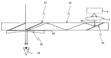
도 1 은 본 발명에서 사용될 수 있는, 평면 기판(20) 및 연관된 컴포넌트(이하, "LOE"라고 지칭됨)를 포함하는 종래 기술의 광학계의 단면도를 도시한다. 광학 수단, 예를 들어 반사면(16)이 광원(미도시)의 디스플레이로부터 시준된 광파(18)에 의해 조명된다. 반사면(16)은 소스로부터의 입사 광을 반사하여, 이 광이 전반사에 의하여 LOE의 평면형 기판(20) 내에 포획되도록 한다. 기판(20)의 하부 및 상부 주면(26, 28)으로부터의 수 차례의 반사 이후에, 포획된 파는 선택적 반사면(22)의 어레이에 도달하는데, 이것은 광을 기판 밖으로, 동공(24)을 가지는 시청자의 눈(25) 안으로 커플링한다. 본 명세서에서, LOE의 입력면은 입력 파가 LOE에 진입하는 데에 통과하는 면으로서 간주될 것이고, LOE의 출력면은 포획된 파가 LOE를 탈출하는 데에 통과하는 면으로서 간주될 것이다. 도 1 에서 예시된 LOE의 경우, 입력 및 출력면 모두가 하부면(26)에 있다. 그러나, 입력 및 이미지 파가 기판(20)의 반대면에 위치될 수 있는 다른 구성, 또는 광이 기판의 기울어진 에지를 통해 LOE 내로 커플링될 경우가 구상된다.1 shows a cross-sectional view of a prior art optical system including a
도 2 에 도시된 바와 같이, 디스플레이 광원(4)으로부터의 s-편광된 입력 광-파(2)가 시준 모듈의 하면(30)을 통해서 시준 모듈(6) 내로 커플링되는데, 이러한 모듈은 보통 광-파 투과 재료로 구성된다. 편광 빔 스플리터(31)의 반사-오프(reflection-off) 이후에, 광파들은 시준 모듈(6)의 면(32)을 통과하여 기판에서 커플링-아웃된다. 그러면, 광파는 사분파장 지연판(34)을 통과하고, 반사 광 소자(36), 예를 들어 평판 미러에 의해 반사되며, 복귀하여 다시 지연판(34)을 통과하고, 면(32)을 통해서 시준 모듈(6)에 재진입한다. 이제 p-편광된 광파는 편광 빔 스플리터(31)를 통하여 지나가고 시준 모듈(6)의 면(38)을 통해 시준 모듈에서 커플링 아웃된다. 그러면 광파는 제 2 사분파장 지연판(40)을 통과하여 지나고, 이것의 반사면(44)에서 컴포넌트(42), 예를 들어 렌즈에 의하여 시준되며, 복귀하여 지연판(34)을 통하여 다시 지나가고, 그리고 면(38)을 통해서 시준 모듈(6)에 재진입한다. 이제 s-편광된 광-파는 편광 빔 분할기(31)에서 반사되고 상부면(46)을 통해서 시준 모듈을 탈출한다. 반사면(36 및 44)은 금속성 또는 유전체 코팅으로 처리될 수 있다.As shown in FIG. 2 , an s-polarized input light-
도 3 은 도 2 에 상세히 도시된 컴포넌트로 구성되는 시준 모듈(6)이 어떻게 기판(20)과 결합되어 광학계를 형성할 수 있는지를 예시한다. 시준 모듈(6)로부터의 출력 광-파(48)는 기판의 하면(26)을 통해 기판(20)에 진입한다. 도 2 에 도시된 바와 같이, 기판(20)에 진입하는 광파는 광학 요소(16)로부터 반사되고 기판 내에 포획된다. 이제, 디스플레이 광원(4), 폴딩 프리즘(52 및 54), 편광 빔 스플리터(31), 지연판(34 및 40) 및 반사 광학 요소(36 및 42)를 포함하는 시준 모듈(6)은, 정확하지 않은 기계적 공차를 가지고서도, 용이하게 단일 기계적 모듈 내에 통합되고 기판으로부터 독립적으로 조립될 수 있다. 추가하여, 지연판(34 및 40) 및 반사 광학 요소(36 및 42)는 각각 함께 접합되어 단일 요소를 형성할 수 있다.FIG. 3 illustrates how a
시준 모듈(6)의 모든 다양한 컴포넌트를 기판(20)에 부착하여, 단순화된 기계적 모듈이 되는 콤팩트한 단일 요소를 형성하는 것이 이로울 것이다. 도 4 는 이러한 모듈을 도시하는데, 시준 모듈(6)의 상면(46)은 경계면(58)에 그리고 기판(20)의 하면(26)에 부착된다. 이러한 구성의 주된 문제점은, 부착 프로시저에 의해 기판(20)과 시준 모듈(6) 사이에 이전에 존재했던 에어 갭(50)(도 3 에 도시됨)을 없앤다는 것이다. 이러한 에어 갭은 입력 광파(48)를 기판(20) 내에 포획하기 위해 필수적인 것이다. 포획된 광파(48)는 경계면(58)의 포인트(62 및 64)에서 반사돼야 한다. 그러므로, 반사 메커니즘이 기판(20)의 주면(26)에서, 또는 시준 모듈(6)의 상면(46)에서 이러한 평면에 적용돼야 한다. 그러나, 이러한 표면들이 예시적인 포인트(66)에서 기판(20)에 진입하거나 진출하는 광파에 대해서 투명하기도 해야 하기 때문에, 단순한 반사 코팅은 쉽게 적용될 수 없다. 광파는 작은 입사각에서 평면(48)을 통과하고 더 높은 입사각에서 반사해야 한다. 보통, 통과하는 입사각은 0° 와 15° 사이이고, 반사하는 입사각은 40° 와 80° 사이이다.It would be advantageous to attach all the various components of the
본 발명의 전술된 실시예에서, LOE 내로 커플링되는 이미지는 무한대로 시준된다. 그러나, 예를 들어 근시가 있고 먼 거리에 위치된 이미지를 적절하게 볼 수 없는 사람을 위해서, 투과된 이미지가 더 가까운 거리로 포커싱되어야 하는 애플리케이션이 존재한다. 도 5 는 본 발명에 따르는, 렌즈를 이용하는 광학계를 예시한다. 무한대로부터 온 이미지(80)는 반사면(16)에 의해 기판(20) 내로 커플링되고, 부분 반사면(22)의 어레이에 의해 시청자의 눈(24) 안으로 반사된다. (평면-오목) 렌즈(82)는 이미지를 편리한 거리에 포커싱하고, 난시를 포함한 시청자의 눈의 다른 수차를 선택적으로 정정한다. 렌즈(82)는 이러한 렌즈(82)의 평탄면(84)에서 기판의 면에 부착될 수 있다. 도 4 와 관련하여 위에서 설명된 바와 같이, 이미지 광파(80)가 전반사에 의해 기판 내에 포획되도록 보장하려면 렌즈와 기판 사이에 얇은 에어 갭이 보존돼야 한다.In the above-described embodiment of the invention, the image coupled into the LOE is collimated to infinity. However, there are applications in which the transmitted image must be focused at a closer distance, for example for people who are nearsighted and cannot properly see images located at a distance. 5 illustrates an optical system using a lens, according to the present invention. An
추가하여, 본 발명에 관련된 대부분의 애플리케이션에서 외부 장면은 무한대에 위치된다고 가정되지만, 외부 장면이 더 가까운 거리에 위치되는 전문 애플리케이션 또는 의학 애플리케이션도 존재한다. 도 6 은 본 발명에 기초하여 듀얼 렌즈 구성을 구현하기 위한 광학계를 예시한다. 무한대로부터 온 이미지 광파(80)는 반사면(16)에 의해 기판(20) 내로 커플링되고, 부분 반사면(22)의 어레이에 의해 시청자의 눈(24) 안으로 반사된다. 가까운 거리에 있는 장면으로부터의 다른 이미지(86)는 렌즈(88)에 의해 무한대로 시준되고, 기판(20)을 지나서 시청자의 눈(24) 안으로 들어간다. 렌즈(82)는 이미지(80 및 86)를 보통(하지만 늘 그런 것은 아님) 외부 장면 이미지의 원래의 거리와 같은 편리한 거리로 포커싱하고, 필요할 경우 시청자의 눈의 다른 수차를 정정한다.In addition, although the external scene is assumed to be located at infinity in most applications related to the present invention, there are also professional or medical applications where the external scene is located at a closer distance. 6 illustrates an optical system for implementing a dual lens configuration based on the present invention.
도 5 및 도 6 에 도시되는 렌즈(82 및 88)는 각각 간단한 평면-오목 및 평면-볼록 렌즈이지만, 기판의 평면형 형상을 유지하기 위해서, 미세한 스텝들이 있는 얇게 몰딩된 플라스틱 판으로 이루어지는 프레넬 렌즈를 대신 사용하는 것이 가능하다. 더욱이, 위에서 설명된 바와 같이 고정된 렌즈를 이용하는 대신에 렌즈(82 또는 88)를 구성하는 다른 방식은 전자적으로 제어되는 동적 렌즈를 사용하는 것이다. 사용자가 시준되지 않은 이미지를 볼 수 있을 뿐만 아니라 이미지의 초점을 동적으로 제어할 수 있을 애플리케이션들이 존재한다. 높은 해상도의 공간 광 변조기(SLM)가 홀로그램 요소를 형성하기 위하여 사용될 수 있다는 것이 밝혀졌다. 현재, 이러한 목적을 위한 가장 인기 있는 소스는 LCD 디바이스이지만, 다른 동적 SLM 디바이스도 역시 사용될 수 있다. 1mm당 수 백 개의 라인을 가지는 높은 해상도의 동적 렌즈가 공지되어 있다. 위에서 도 5 및 도 6 과 함께 전술된 고정된 렌즈 대신에 이러한 종류의 전자-광학적으로 제어되는 렌즈가 본 발명에 있는 원하는 동적 요소로서 사용될 수 있다. 그러므로, 실시간으로, 사용자는 기판에 의해 투영된 가상 이미지 및 외부 뷰의 실제 이미지 양자 모두의 정확한 초점면을 결정하고 설정할 수 있다.
도 6 에 도시된 바와 같이, 렌즈(82 및 88)를 기판(20)에 부착하여 단일하고 콤팩트한 단순화된 기계적 모듈을 형성하는 것이 이로울 것이다. 전술된 바와 같은 주된 문제점은 부착 프로시저에 의해 기판(20)과 렌즈(82 및 88) 사이에 이전에 존재했던 에어 갭이 사라진다는 것이라는 것이 분명하고, 이러한 갭은 이미지 광파(80)를 기판(20) 내에 포획하기 위해 필수적인 것이다. 포획된 이미지 광파(80)는 경계면(84)의 포인트(90)에서 반사되고 포인트(92)에서 같은 면을 통해 투과돼야 한다. 그러므로, 도 4 와 관련하여 위에서 설명된 바와 같은 유사한 부분 반사형 메커니즘이 이러한 평면에 적용되어야 한다.As shown in FIG. 6 , it would be advantageous to attach
요구되는 부분 반사형 메커니즘을 얻기 위해서, 각도 감응 박막 코팅을 기판의 주면에 도포하는 것이 가능하지만, 이러한 실시예를 제작하는 것은 복잡하고 고비용일 수 있다. 요구되는 부분 반사형 메커니즘을 구현하기 위한 다른 방법은, 도 7a 및 도 7b 에 도시된 바와 같이 투명 에어 갭 필름(110)을 기판의 주면에 부착하는 것이다. 에어 갭 필름이라는 용어는 명소 지역의 파장 보다 더 짧은 작은 피치로 배치된 투명 유전체 재료의 초미세 주기적 구조체(111)를 그 자신의 표면에 가지는 광학 디바이스를, 예를 들어 평탄한 투명 기판(112)(이하, "베이스"(112) 또는 "베이스 필름"(112)이라고 불림) 상에 형성된 조밀한 (요철) 초미세 주기적 구조체(111)(이하, "요철 형상"이라고 불림)를 가지는 모스 아이 필름과 같은 광학 디바이스와 관련된다. 요철 형상의 높이는 1 마이크론 미만인 것이 바람직하다(하지만 반드시 그래야 하는 것은 아니다).Although it is possible to apply an angle-sensitive thin film coating to the major surface of the substrate to achieve the desired partially reflective mechanism, fabricating such an embodiment can be complex and expensive. Another way to implement the required partially reflective mechanism is to attach the transparent
도 8a 및 도 8b 에서 볼 수 있는 바와 같이, 에어 갭 필름(110)의 표면과 평행한 임의의 단면(121)은 주기적 형상을 가지는데, 요철 형상 내의 유전체 재료(123)의 비율분(proportional portion)은 필름 자체의 함수로서 점진적으로 변경된다.As can be seen in FIGS. 8A and 8B , any
도 9a 와 도 9b 및 도 10a 와 10b에서 더 알 수 있는 바와 같이, 베이스 필름(112)에 더 가까운 내부 단면(124), 즉 초미세 구조체(111)의 하부에서 요철 형상(126) 내의 유전체 재료(125)의 비율분은 최대이고 실질적으로 1 에 가까운 반면에, 외부 단면(127), 즉 초미세 구조체(111)의 상부에 가까운 곳에서, 요철 형상(129) 내의 유전체 재료(128)의 비율분은 최소, 즉 재료(125)에서보다 훨씬 낮은 값이고 실질적으로 제로와 같다.As can be further seen in FIGS. 9A and 9B and FIGS. 10A and 10B , the dielectric material in the
통상적으로, 광파가 주기적 구조체를 가지는 광학 디바이스를 통과할 경우, 광의 회절이 발생하고 회절된 광의 제로차수, 즉 회절이 없이 디바이스를 통과해서 투과되는 광의 휘도는 상당히 감소된다. 그러나, 초미세 주기적 구조체의 피치가 인입하는 광파의 파장 보다 훨씬 짧으면, 회절은 발생하지 않는다. 그 대신에, 광학 파가 매질이 이러한 매질에 포함된 재료의 평균인 굴절률을 가진다고 "인식(see)"하기 때문에, 효과적인 반사 방지 특성을 얻을 수 있다.Typically, when a light wave passes through an optical device having a periodic structure, diffraction of the light occurs and the zero order of the diffracted light, ie the luminance of light transmitted through the device without diffraction, is significantly reduced. However, if the pitch of the ultrafine periodic structure is much shorter than the wavelength of the incoming light wave, no diffraction occurs. Instead, because the optical wave "sees" that the medium has a refractive index that is the average of the materials contained in this medium, effective antireflection properties can be obtained.
반면에, 도 11 에 도시된 바와 같이, 광파(130)가 비스듬한 각도에서 구조체의 상부측에서 주기적 초미세 구조체(111)에 충돌하면, 광파(130)는 투명 재료의 비율분이 매우 낮은 주기적 구조체의 외부 부분만을 "바라보게(see)" 된다. 그러므로, 인입하는 광학적 파가 "느끼는(seen)" 실제 굴절률은 공기(131)의 굴절률에 가깝다.On the other hand, as shown in FIG. 11 , when the
결과적으로, 그리고 도 12 에 도시된 바와 같이, 이러한 에어-갭 필름이 기판(20)의 외부면(28)에 부착되면, 커플링된 광파(130)는 기판과 필름 사이의 경계면(132)에 임계 각도보다 높은 각도도 충돌하고, 필름과 기판 사이에 구속된 공기(131)가 경계 표면에서의 공기와 유사한 굴절률 때문에 광학적 격리를 제공한다. 그러므로, 외부면으로부터의 커플링-인된 광파의 전반사 현상들이 보존될 것이고 광파는 기판 내에 보유될 것이다.As a result, and as shown in FIG. 12 , when this air-gap film is attached to the
구조체의 높이, 피크-피크 및 폭과 같은 초미세 구조체의 기하학적 특성은 보통 10 내지 800 나노미터 사이에 있을 수 있다. 추가적으로, 초미세 구조체의 정확한 형상은 반드시 모스 아이의 형상일 필요가 없다. 피라미드, 프리즘, 원뿔 등과 같은 임의의 다른 나노-구조 형상이 사용될 수도 있다. 더 나아가, 주기적 구조체가 보통 제작하기가 더 쉽긴 하지만, 초미세 구조체는 엄격하게 주기적이어야 하는 것도 아니다. 그러나, 이러한 초미세 구조체는 다음의 요구 사항을 만족해야 한다: 일면으로는, 구조체는 부착 프로세스 중에 파괴되지 않을 만큼 충분히 고형물이어야 하고, 다른 면으로는, 구조체의 외부 단면에 있는 유전체 재료의 비율분은 기판 내의 전반사 현상을 유지하기 위해서 실질적으로 제로와 같아야 한다. 추가하여, 초미세 구조체의 기본 요소의 크기는 회절 효과를 피하기 위해서 너무 크지 않아야 한다. 그러나, 초미세 구조체의 두께를 100 nm 아래로 줄이면 포획된 파가 원치 않게 에어 갭 필름을 통과할 수 있고 전반사 현상들이 깨질 수 있다. 결과적으로, 초미세 구조체 두께에 대한 통상적인 요구된 값은 200 내지 300 nm 사이이다.The geometrical properties of the ultrafine structure, such as the height, peak-to-peak and width of the structure, can usually be between 10 and 800 nanometers. Additionally, the exact shape of the ultrafine structure does not necessarily have to be that of a moth's eye. Any other nano-structured shape may be used, such as pyramids, prisms, cones, and the like. Furthermore, although periodic structures are usually easier to fabricate, ultrafine structures do not have to be strictly periodic. However, these ultrafine structures must meet the following requirements: on the one hand, the structure must be sufficiently solid not to break during the attachment process, and on the other hand, the proportion of dielectric material in the outer cross-section of the structure. must be substantially equal to zero to maintain total reflection within the substrate. In addition, the size of the elementary element of the ultrafine structure should not be too large to avoid diffraction effects. However, if the thickness of the ultrafine structure is reduced below 100 nm, the trapped waves may undesirably pass through the air gap film and the total reflection phenomena may be broken. Consequently, a typical required value for the ultrafine structure thickness is between 200 and 300 nm.
도 13a 는 안경 시스템(140)의 전면 뷰를 도시하고, 도 13b 는 두 개의 광학 렌즈(141, 142) 사이에 임베딩되고 안경테(143) 내에 조립된 기판(20)의 상면도를 도시한다. 도시된 바와 같이, 광학 요소에 추가하여, 테는 카메라(144), 마이크로폰(145), 이어폰(146), USB 커넥터, 메모리 카드, 관성 측정 유닛(IMU), 등의 다른 부속물을 포함할 수 있다.13A shows a front view of the
도 14a, 도 14b 및 도 14c 는 접착제가 없이 테(154) 안에 함께 탑재된 전면 양의 렌즈(151)와 후면 음의 렌즈(152) 사이에 임베딩된 기판(20)을 포함하는 비-모놀리식 광학 요소(150)를 도시한다. 에어 갭 필름(110)(도 14c)은 기판(20)과 렌즈(151, 152) 사이에 배치되거나 결합되는데, 초미세 구조체들(111)은 기판(20)의 외부면(26 및 28)을 각각 바라본다. 에어 갭 필름(110)은 압력-감응 접착제(PSA)를 사용하여 광학 렌즈(151 및 152)의 평면형 표면에 직접적으로 접합될 수 있고, 또는 엠보싱, 사출 성형, 주물, 머시닝, 소프트 리소그래피 또는 임의의 다른 직접적 제작 방법을 사용하여 렌즈의 일체형 부분으로서 직접적으로 제조될 수 있다. 임베딩된 광학 요소(150)는 압력 또는 접합 기법을 이용하여 테(154) 안에 조립될 수 있다.14A, 14B, and 14C show a
기판(20)을 두 개의 광학 렌즈들 사이에 일체형으로 임베딩하기 위한 다른 방법이 도 15a, 도 15b 및 도 15c 에 도시된다. 기판(20)은 외주 결합 기법을 이용하여 광학 렌즈들 사이에 임베딩된다. 전면 렌즈(151) 및 후면 렌즈(152)는 모든 컴포넌트를 함께 탑재시키는 비-광학적 접착제 또는 임의의 다른 높은-점성 접착제(156)를 사용하여 기판(20)의 주변 에지에 접합된다. 접착제의 점성은 필름(110)과 기판(20) 사이에 구속된 에어 포켓(131)내로 접착제가 누설되지 않게 하기 위해서 충분히 커야 한다. 이러한 누설이 생기면, 기판의 외부면으로부터의 광파의 전반사를 보존하기 위해서 요구되는 에어 갭이 없어질 수 있다. 요구된 접착제(156)는, 예를 들어 OP-67-LS 또는 임의의 실온 가황(room temperature vulcanization; RTV) 실리콘일 수 있다.Another method for integrally embedding a
두 개의 광학 렌즈들 사이에 기판(20)을 일체형으로 임베딩하기 위한 다른 대안적인 방법이 도 16a, 도 16b 및 도 16c 에 도시된다. 임베딩된 요소의 생산 프로시저는 다음과 같다: 초미세 구조체(111)가 기판(20)의 외부면(26 및 28)을 바라보게 에어 갭 필름(110)을 배치한다; 정전기와 같은 부착 기법을 이용한다; 요소의 요구된 외부 형상을 가지는 몰드(160)를 준비한다; 기판(20)을 몰드 안에 삽입한다; 폴리머를 몰드 내에 캐스팅하거나 주입하고, UV에 의하여 또는 폴리머 온도를 변경하여 폴리머를 경화시킨다; 그리고 마지막으로, 임베딩된 요소를 몰드로부터 방출한다. 도 15a 내지 도 15c 와 관련하여 위에서 설명된 바와 같이, 기판(20)과 에어 갭 필름(110) 사이의 에어 포켓(131)으로 재료가 누설되는 것을 막기 위해서 초미세 지역이 사출 성형 프로세스 중에 주입된 재료로부터 격리되는 것도 역시 중요하다.Another alternative method for integrally embedding the
도 13a 내지 도 16c 가 두 개의 광학 렌즈들 사이에 임베딩된 기판을 포함하는 광학 컴포넌트를 형성하기 위한 다양한 방법들을 예시하지만, 평면 요소를 기판의 외부면에 부착할 필요가 있는 실시예도 존재한다. 이러한 실시예의 일 예가 도 4 에 도시되는데, 여기에서 시준 요소(6)는 기판(20)에 부착된다. 평탄한 요소를 기판에 부착하는 다른 이유는, 사용자의 눈의 안전성을 향상시키기 위해서 기판을 기계적으로 보호하는 것, 또는 평탄한 요소의 외부면에 코팅을 도포하여 광색성 응답성(photochromic response), 스크래치 저항성, 높은 친수성, 유색(가색) 뷰, 편광, 지문 방지 등과 같은 다양한 특성을 얻는 것일 수 있다.Although FIGS. 13A-16C illustrate various methods for forming an optical component that includes a substrate embedded between two optical lenses, there are also embodiments where it is necessary to attach a planar element to the outer surface of the substrate. An example of such an embodiment is shown in FIG. 4 , in which a
두 개의 평탄한 기판(162 및 164) 사이에 임베딩되고 테(166, 167) 안에 조립된 기판(20)이 도 17a, 도 17b 및 도 17c 에 도시된다. 기판 및 평탄한 기판(20)의 임베딩 프로세스는 기계적 부착, 주변 접합 또는 모놀리식 제작법을 사용하여 구체화될 수 있다. 임베딩 프로세스는 기판의 외부면들 중 하나에 하나의 요소만을 부착하는 것 또는 평탄한 기판 및 만곡형 렌즈와 같은 상이한 요소들을 결합하는 것을 포함할 수 있다.A
지금까지 예시된 모든 실시예에서, 광파를 기판 밖으로 커플링하기 위한 요소는 상기 기판 내에 위치되는 적어도 하나의 평탄한 부분 반사면인데, 이것은 보통 부분 반사형 유전체 코팅으로 코팅되고 상기 기판의 주면과 평행하지 않다. 그러나, 본 발명에 따르는 특수 반사성 메커니즘이 다른 커플링-아웃 기술을 위해 활용될 수 있다. 도 18 은 커플링-인 요소(170) 또는 커플링-아웃 요소(172)가 회절 요소인 기판(20)을 도시한다. 추가하여, 만곡형 부분 반사면, 및 다른 수단과 같은 다른 커플링-아웃 요소가 사용될 수 있다.In all of the embodiments illustrated so far, the element for coupling the light wave out of the substrate is at least one planar partially reflective surface located within the substrate, which is usually coated with a partially reflective dielectric coating and is not parallel to the major surface of the substrate. not. However, special reflective mechanisms according to the present invention may be utilized for other coupling-out techniques. 18 shows a
도 13 내지 도 17 의 실시예들은 본 발명의 간단한 구현형태를 예시하는 예들일 뿐이다. 시스템의 코어를 구성하는 기판-유도형(guided) 광학 요소가 매우 콤팩트하고 경량이기 때문에, 매우 다양한 장치에 설치될 수 있다. 차양, 폴딩 디스플레이, 단안경(monocle), 및 더 많은 것을 포함하는 많은 다른 실시예들도 역시 가능하다. 이러한 실시예는 디스플레이가 눈에 가깝거나; 머리에 탑재되거나, 머리 위에 쓰거나, 머리로 운반돼야 하는 애플리케이션들에 대해 지정된다. 그러나, 디스플레이가 이와 달리 위치되는 애플리케이션들도 존재한다. 이러한 애플리케이션의 일 예는 예를 들어 스마트 폰 또는 스마트워치와 같은, 모바일 애플리케이션을 위한 손으로 운반되는 디바이스이다. 이러한 스마트 디바이스의 주된 문제는 크기와 부피가 작아야 한다는 것과 이미지의 품질이 높아야 한다는 가치의 충돌이다.The embodiments of FIGS. 13 to 17 are merely examples illustrating simple implementations of the present invention. Since the substrate-guided optical elements constituting the core of the system are very compact and lightweight, they can be installed in a wide variety of devices. Many other embodiments are also possible, including sunshades, folding displays, monocles, and more. Such an embodiment may be such that the display is close to the eye; It is specified for applications that must be mounted on the head, worn over the head, or carried over the head. However, there are also applications in which the display is otherwise positioned. An example of such an application is a hand-carried device for mobile applications, such as, for example, a smart phone or smartwatch. The main problem with these smart devices is the clash of values between small size and volume and high image quality.
도 19 는 모바일 디바이스의 작은 크기와 풀 포맷 디스플레이에서 디지털 콘텐츠를 시청하려는 희망을 절충하기 위해 현재 필요한 불이익을 제거하는, 본 발명에 기초한 다른 방법을 예시한다. 이러한 애플리케이션은 모바일 디바이스를 작게 하면서 풀 포맷 디스플레이에서 디지털 콘텐츠를 보고 싶어 한다는 과거의 상반된 요구 사항을 고품질 이미지를 사용자의 눈에 직접 투영함으로써 해결하는 핸드-헬드 디스플레이(hand-held display; HHD)이다. 광학 모듈은 디스플레이 소스(4), 폴딩 및 시준 광학기(190)를 포함하고, 기판(20)은 스마트 디바이스(210)의 몸체 내에 통합되는데, 기판(20)이 전화기의 현존하는 보호 커버-윈도우를 대체한다. 구체적으로 설명하면, 소스(4) 및 광학기(190)를 포함하는 지원 컴포넌트의 부피는 현대의 스마트 디바이스의 수락가능한 부피 안에 맞춤될 만큼 충분히 작다. 디바이스에 의해 송출된 풀 스크린을 보기 위해서, 디바이스의 윈도우는 높은 FOV, 큰 눈-모션-박스 및 쾌적한 눈동자 거리(eye-relief)를 가지고 이미지를 관찰하는 사용자의 눈(24) 앞에 위치된다. 이미지의 다른 부분을 디스플레이하도록 디바이스를 틸팅함으로써 더 큰 눈동자 거리에서 전체 FOV를 시청하는 것도 역시 가능하다. 더 나아가, 광학 모듈이 시스루 구조에서 작동할 수 있기 때문에, 디바이스의 듀얼 동작이 가능하다; 즉 종래의 디스플레이(212)를 온전히 유지하는 옵션이 존재한다. 이러한 방식으로, 디스플레이 소스(4)가 셧오프된 경우 기판(20)을 통해서 표준 디스플레이가 시청될 수 있다. 방대한 인터넷 서핑 또는 고품질 비디오 동작을 위해 지정되는 제 2 의 가상-모드에서, 종래의 디스플레이(212)는 셧오프되는 반면에, 디스플레이 소스(4)는 요구된 넓은 FOV 이미지를 기판(20)을 통해 시청자의 눈 안으로 투영시킨다. 보통, 손으로 운반되는 대부분의 스마트 디바이스에서, 사용자는 디바이스의 전면 윈도우에 임베딩된 터치스크린을 사용하여 스마트 디바이스를 작동시킬 수 있다. 도 19 에 도시된 바와 같이, 터치스크린(220)은 기판(20) 상에 위치된 외부면 에어 갭 필름(110) 상에 터치스크린을 직접 접합함으로써 스마트 디바이스에 부착될 수 있다.19 illustrates another method based on the present invention, which eliminates the penalty currently necessary for balancing the small size of a mobile device with the desire to view digital content on a full format display. One such application is a hand-held display (HHD) that addresses the previously conflicting requirement of viewing digital content on a full-format display while making mobile devices smaller by projecting high-quality images directly onto the user's eyes. The optical module comprises a
Claims (33)
적어도 두 개의 외부 주면 및 에지를 가지는 광-투과성 기판(20);
내부 반사에 의해 광파(48)를 상기 기판 내로 커플링하기 위한 광학 요소(16);
광파를 상기 기판 밖으로 커플링하기 위한, 상기 기판 내에 위치된 적어도 하나의 부분 반사면(22); 및
베이스(112) 및 상기 베이스 상에 구성된 요철 형상(relief formation)을 형성하는 초미세 구조체(hyperfine structure)(111)를 포함하는 적어도 하나의 투명 에어 갭 필름(110)을 포함하되, 상기 요철 형상이 상기 기판을 바라보면서 경계면을 형성하도록 상기 에어 갭 필름(110)이 상기 기판의 주면들 중 하나에 부착되어, 상기 기판 내에 커플링된 광파가 상기 경계면으로부터 실질적으로 전반사되게 하고,
상기 베이스에 평행한 단면에서의 상기 요철 형상의 비율분(proportional portion)은, 상기 베이스로부터의 상기 단면의 거리의 함수로서 점진적으로 변하는, 광학계.As an optical system,
a light-transmissive substrate 20 having at least two outer major surfaces and an edge;
an optical element (16) for coupling a light wave (48) into the substrate by internal reflection;
at least one partially reflective surface (22) positioned within the substrate for coupling a light wave out of the substrate; and
at least one transparent air gap film 110 comprising a base 112 and a hyperfine structure 111 forming a relief formation configured on the base, wherein the relief formation is the air gap film 110 is attached to one of the major surfaces of the substrate to form an interface while facing the substrate, such that light waves coupled within the substrate are substantially totally reflected from the interface,
and a proportional portion of the concave-convex shape in a cross-section parallel to the base varies gradually as a function of the distance of the cross-section from the base.
상기 에어 갭 필름은 상기 요철 형상과 기판 사이에 에어 포켓을 형성하는, 광학계.The method of claim 1,
The air gap film forms an air pocket between the concave-convex shape and the substrate.
상기 요철 형상은 유전체 재료를 포함하는, 광학계.The method of claim 1,
The concave-convex shape includes a dielectric material.
상기 요철 형상의 유전체 재료의 비율분은 상기 베이스에 근접한 내부 단면에서 최대인, 광학계.4. The method of claim 3,
and a proportion of the concave-convex-shaped dielectric material is maximum in an inner cross section close to the base.
상기 요철 형상의 유전체 재료의 비율분은 상기 베이스에 근접한 내부 단면에서 실질적으로 1과 같은, 광학계.4. The method of claim 3,
and a proportion of the concave-convex dielectric material is substantially equal to one in an inner cross-section proximate to the base.
상기 요철 형상의 유전체 재료의 비율분은 상기 경계면에 근접한 외부 단면에서 최소인, 광학계.4. The method of claim 3,
and a proportion of the concave-convex-shaped dielectric material is minimum in an outer cross-section close to the interface.
상기 요철 형상의 유전체 재료의 비율분은 상기 경계면에 근접한 외부 단면에서 실질적으로 0과 같은, 광학계.8. The method of claim 7,
and a proportion of the concave-convex-shaped dielectric material is substantially equal to zero in an outer cross-section proximate to the interface.
상기 경계면에 근접한 외부 단면에서의 상기 요철 형상의 굴절률은 공기의 굴절률과 실질적으로 같은, 광학계.The method of claim 1,
and the refractive index of the concave-convex shape in the outer cross section close to the interface is substantially equal to the refractive index of air.
상기 요철 형상은 주기적 요철 형상인, 광학계.The method of claim 1,
The concave-convex shape is a periodic concavo-convex shape.
상기 요철 형상은 모스 아이(moth eye)의 구조를 가지고 및/또는 프리즘, 원뿔 및 피라미드의 어레이들의 군으로부터 선택되는, 광학계.The method of claim 1,
wherein the concave-convex shape has the structure of a moth eye and/or is selected from the group of arrays of prisms, cones and pyramids.
상기 초미세 구조체의 기하학적 특성은, (a) 인입하는 광파의 파장보다 작은 것, (b) 나노구조 필름 및 (c) 10 내지 800 나노미터 범위로 이루어진 군에서 선택되는, 광학계.The method of claim 1,
The geometrical properties of the ultrafine structure are selected from the group consisting of (a) less than the wavelength of an incoming light wave, (b) a nanostructured film, and (c) a range of 10 to 800 nanometers.
상기 요철 형상의 높이는 1 마이크론 미만인, 광학계.The method of claim 1,
The height of the concave-convex shape is less than 1 micron.
상기 광학계는, 상기 기판을 바라보는 적어도 하나의 평탄한 외부면을 가지는 적어도 하나의 광학 요소를 더 포함하고,
상기 베이스는 상기 요소의 외부면 및 상기 기판을 바라보는 요철 형상에 광학적으로 접합되는, 광학계.The method of claim 1,
The optical system further comprises at least one optical element having at least one flat outer surface facing the substrate,
and the base is optically bonded to an outer surface of the element and a concave-convex shape facing the substrate.
상기 광학계는, 상기 요철 형상이 기판 표면을 바라보면서 상기 광-투과성 기판의 주면들 중 제 2 주면에 부착되는 제 2 에어 갭 필름을 더 포함하는, 광학계.The method of claim 1,
The optical system further comprises a second air gap film attached to a second main surface of the main surfaces of the light-transmitting substrate while the concave-convex shape faces the substrate surface.
상기 광학계는, 적어도 하나의 평탄면을 각각 가지는 두 개의 렌즈를 더 포함하고,
상기 제 1 및 제 2 에어 갭 필름의 베이스들은 상기 렌즈의 평탄면에 접합되는, 광학계.16. The method of claim 15,
The optical system further comprises two lenses each having at least one flat surface,
and the bases of the first and second air gap films are bonded to the flat surface of the lens.
광파를 기판 밖으로 커플링하기 위한 상기 부분 반사면은 곡면인, 광학계.The method of claim 1,
wherein the partially reflective surface for coupling the light wave out of the substrate is a curved surface.
Applications Claiming Priority (3)
| Application Number | Priority Date | Filing Date | Title |
|---|---|---|---|
| IL235642A IL235642B (en) | 2014-11-11 | 2014-11-11 | Compact head-mounted display system protected by a hyperfine structure |
| IL235642 | 2014-11-11 | ||
| PCT/IL2015/051087 WO2016075689A1 (en) | 2014-11-11 | 2015-11-10 | Compact head-mounted display system protected by a hyperfine structure |
Publications (2)
| Publication Number | Publication Date |
|---|---|
| KR20170080695A KR20170080695A (en) | 2017-07-10 |
| KR102323870B1 true KR102323870B1 (en) | 2021-11-09 |
Family
ID=52594870
Family Applications (1)
| Application Number | Title | Priority Date | Filing Date |
|---|---|---|---|
| KR1020177015688A KR102323870B1 (en) | 2014-11-11 | 2015-11-10 | Compact head-mounted display system protected by a hyperfine structure |
Country Status (11)
| Country | Link |
|---|---|
| US (3) | US10520731B2 (en) |
| EP (2) | EP3218751B1 (en) |
| JP (1) | JP6759224B2 (en) |
| KR (1) | KR102323870B1 (en) |
| CN (2) | CN107111132B (en) |
| BR (1) | BR112017009652B1 (en) |
| CA (1) | CA2966851C (en) |
| IL (1) | IL235642B (en) |
| RU (1) | RU2689255C2 (en) |
| SG (1) | SG11201703507PA (en) |
| WO (1) | WO2016075689A1 (en) |
Families Citing this family (87)
| Publication number | Priority date | Publication date | Assignee | Title |
|---|---|---|---|---|
| IL166799A (en) | 2005-02-10 | 2014-09-30 | Lumus Ltd | Substrate-guided optical device utilizing beam splitters |
| US10073264B2 (en) | 2007-08-03 | 2018-09-11 | Lumus Ltd. | Substrate-guide optical device |
| US10048499B2 (en) | 2005-11-08 | 2018-08-14 | Lumus Ltd. | Polarizing optical system |
| IL232197B (en) | 2014-04-23 | 2018-04-30 | Lumus Ltd | Compact head-mounted display system |
| IL235642B (en) | 2014-11-11 | 2021-08-31 | Lumus Ltd | Compact head-mounted display system protected by a hyperfine structure |
| NZ734365A (en) * | 2015-01-22 | 2020-06-26 | Magic Leap Inc | Methods and system for creating focal planes using an alvarez lens |
| IL237337B (en) | 2015-02-19 | 2020-03-31 | Amitai Yaakov | Compact head-mounted display system having uniform image |
| EP3062142B1 (en) | 2015-02-26 | 2018-10-03 | Nokia Technologies OY | Apparatus for a near-eye display |
| JP6877363B2 (en) * | 2015-05-19 | 2021-05-26 | マジック リープ, インコーポレイテッドMagic Leap,Inc. | Illuminator |
| US9946074B2 (en) * | 2016-04-07 | 2018-04-17 | Google Llc | See-through curved eyepiece with patterned optical combiner |
| CN109154720A (en) * | 2016-05-18 | 2019-01-04 | 鲁姆斯有限公司 | Wear-type imaging device |
| CN107783290B (en) * | 2016-08-30 | 2023-12-29 | 北京亮亮视野科技有限公司 | Head-mounted visual device capable of performing retina projection |
| JP6665943B2 (en) * | 2016-09-21 | 2020-03-13 | 日本精機株式会社 | Head-up display device |
| AU2017301074B2 (en) | 2016-10-09 | 2022-02-03 | Lumus Ltd | Aperture multiplier using a rectangular waveguide |
| RU2763850C2 (en) | 2016-11-08 | 2022-01-11 | Люмус Лтд | Lightguide device with edge providing optical cutoff and corresponding manufacturing methods |
| US10650552B2 (en) | 2016-12-29 | 2020-05-12 | Magic Leap, Inc. | Systems and methods for augmented reality |
| EP4300160A2 (en) | 2016-12-30 | 2024-01-03 | Magic Leap, Inc. | Polychromatic light out-coupling apparatus, near-eye displays comprising the same, and method of out-coupling polychromatic light |
| US11500143B2 (en) | 2017-01-28 | 2022-11-15 | Lumus Ltd. | Augmented reality imaging system |
| WO2018154576A1 (en) | 2017-02-22 | 2018-08-30 | Lumus Ltd. | Light guide optical assembly |
| EP3376279B1 (en) * | 2017-03-13 | 2022-08-31 | Essilor International | Optical device for a head-mounted display, and head-mounted device incorporating it for augmented reality |
| KR20230025946A (en) | 2017-03-22 | 2023-02-23 | 루머스 리미티드 | Overlapping facets |
| IL251645B (en) | 2017-04-06 | 2018-08-30 | Lumus Ltd | Light-guide optical element and method of its manufacture |
| CN110573932B (en) | 2017-06-06 | 2022-08-23 | 苹果公司 | Optical system for electronic device with display |
| WO2019016813A1 (en) | 2017-07-19 | 2019-01-24 | Lumus Ltd. | Lcos illumination via loe |
| US10578870B2 (en) | 2017-07-26 | 2020-03-03 | Magic Leap, Inc. | Exit pupil expander |
| CN111183393B (en) | 2017-09-29 | 2024-03-19 | 鲁姆斯有限公司 | Augmented reality display |
| CN111133362B (en) | 2017-10-22 | 2021-12-28 | 鲁姆斯有限公司 | Head-mounted augmented reality device employing optical bench |
| KR102570722B1 (en) | 2017-11-21 | 2023-08-24 | 루머스 리미티드 | Optical Aperture Expansion Array for Near Eye Displays |
| WO2019106637A1 (en) | 2017-12-03 | 2019-06-06 | Lumus Ltd. | Optical device alignment methods |
| CA3084811A1 (en) | 2017-12-10 | 2019-06-13 | Magic Leap, Inc. | Anti-reflective coatings on optical waveguides |
| CA3086206A1 (en) | 2017-12-20 | 2019-06-27 | Magic Leap, Inc. | Insert for augmented reality viewing device |
| WO2019135169A1 (en) | 2018-01-02 | 2019-07-11 | Lumus Ltd. | Augmented reality displays with active alignment and corresponding methods |
| US10551544B2 (en) | 2018-01-21 | 2020-02-04 | Lumus Ltd. | Light-guide optical element with multiple-axis internal aperture expansion |
| WO2019178567A1 (en) | 2018-03-15 | 2019-09-19 | Magic Leap, Inc. | Image correction due to deformation of components of a viewing device |
| CN108490611B (en) * | 2018-03-26 | 2020-12-08 | 京东方科技集团股份有限公司 | Method and device for adjusting refraction of augmented reality equipment and augmented reality equipment |
| WO2019197959A1 (en) | 2018-04-08 | 2019-10-17 | Lumus Ltd. | Optical sample characterization |
| CN112119346B (en) | 2018-05-14 | 2022-08-19 | 鲁姆斯有限公司 | Projector arrangement with subdivided optical aperture for a near-eye display and corresponding optical system |
| WO2019220386A1 (en) | 2018-05-17 | 2019-11-21 | Lumus Ltd. | Near-eye display having overlapping projector assemblies |
| IL259518B2 (en) | 2018-05-22 | 2023-04-01 | Lumus Ltd | Optical system and method for improvement of light field uniformity |
| CN112119345A (en) | 2018-05-23 | 2020-12-22 | 鲁姆斯有限公司 | Optical system comprising a light-guiding optical element having a partially reflective inner surface |
| US11885871B2 (en) | 2018-05-31 | 2024-01-30 | Magic Leap, Inc. | Radar head pose localization |
| CN112313499A (en) | 2018-06-21 | 2021-02-02 | 鲁姆斯有限公司 | Measurement technique for refractive index non-uniformity between plates of light guide optical element (LOE) |
| US11415812B2 (en) | 2018-06-26 | 2022-08-16 | Lumus Ltd. | Compact collimating optical device and system |
| WO2020010097A1 (en) | 2018-07-02 | 2020-01-09 | Magic Leap, Inc. | Pixel intensity modulation using modifying gain values |
| US11856479B2 (en) | 2018-07-03 | 2023-12-26 | Magic Leap, Inc. | Systems and methods for virtual and augmented reality along a route with markers |
| US11510027B2 (en) | 2018-07-03 | 2022-11-22 | Magic Leap, Inc. | Systems and methods for virtual and augmented reality |
| CN112424670B (en) | 2018-07-16 | 2023-01-17 | 鲁姆斯有限公司 | Light guide optical element employing polarizing internal reflector |
| WO2020023545A1 (en) | 2018-07-24 | 2020-01-30 | Magic Leap, Inc. | Temperature dependent calibration of movement detection devices |
| US11624929B2 (en) | 2018-07-24 | 2023-04-11 | Magic Leap, Inc. | Viewing device with dust seal integration |
| EP3831058A4 (en) | 2018-08-02 | 2022-04-20 | Magic Leap, Inc. | A viewing system with interpupillary distance compensation based on head motion |
| EP3830631A4 (en) | 2018-08-03 | 2021-10-27 | Magic Leap, Inc. | Unfused pose-based drift correction of a fused pose of a totem in a user interaction system |
| US11543583B2 (en) | 2018-09-09 | 2023-01-03 | Lumus Ltd. | Optical systems including light-guide optical elements with two-dimensional expansion |
| CN113168017A (en) * | 2018-09-21 | 2021-07-23 | 谷歌有限责任公司 | Optical combination lens for wearable head-up display |
| EP3853654A1 (en) * | 2018-09-21 | 2021-07-28 | Dolby Laboratories Licensing Corporation | Incorporating components inside optical stacks of head-mounted devices |
| US11262585B2 (en) * | 2018-11-01 | 2022-03-01 | Google Llc | Optical combiner lens with spacers between lens and lightguide |
| CN112969955B (en) | 2018-11-08 | 2023-05-26 | 鲁姆斯有限公司 | Optical device and system with dichroic beam splitter color combiner |
| TWM642752U (en) | 2018-11-08 | 2023-06-21 | 以色列商魯姆斯有限公司 | Light-guide display with reflector |
| KR20200001026U (en) | 2018-11-11 | 2020-05-21 | 루머스 리미티드 | Near eye display with intermediate window |
| US11221486B2 (en) * | 2018-12-10 | 2022-01-11 | Auroratech Company | AR headsets with improved pinhole mirror arrays |
| US20220075118A1 (en) * | 2018-12-21 | 2022-03-10 | Magic Leap, Inc. | Air pocket structures for promoting total internal reflection in a waveguide |
| CN109445109A (en) * | 2018-12-26 | 2019-03-08 | 深圳珑璟光电技术有限公司 | A kind of light-transmitting plate |
| CN113325507A (en) * | 2018-12-26 | 2021-08-31 | 上海鲲游光电科技有限公司 | Planar optical waveguide based on two-dimensional grating |
| CN110146980A (en) * | 2018-12-29 | 2019-08-20 | 深圳珑璟光电技术有限公司 | A kind of substrate-guided optical device |
| GB201900652D0 (en) * | 2019-01-17 | 2019-03-06 | Wave Optics Ltd | Augmented reality system |
| US10983264B2 (en) | 2019-01-24 | 2021-04-20 | Lumus Ltd. | Optical systems including light-guide optical elements with two-dimensional expansion |
| IL264551A (en) * | 2019-01-29 | 2020-07-30 | Amitai Yaakov | Highly efficient compact head-mounted display system having small input aperture |
| WO2020185405A1 (en) | 2019-03-12 | 2020-09-17 | Magic Leap, Inc. | Registration of local content between first and second augmented reality viewers |
| KR102651647B1 (en) | 2019-03-12 | 2024-03-26 | 루머스 리미티드 | image projector |
| US20220091420A1 (en) * | 2019-04-23 | 2022-03-24 | Directional Systems Tracking Limited | Augmented reality system |
| US11927872B2 (en) | 2019-06-23 | 2024-03-12 | Lumus Ltd. | Display with foveated optical correction |
| CA3137994A1 (en) | 2019-06-27 | 2020-12-30 | Lumus Ltd | Apparatus and methods for eye tracking based on eye imaging via a light-guide optical element |
| US11514673B2 (en) | 2019-07-26 | 2022-11-29 | Magic Leap, Inc. | Systems and methods for augmented reality |
| US11737832B2 (en) | 2019-11-15 | 2023-08-29 | Magic Leap, Inc. | Viewing system for use in a surgical environment |
| KR20240008402A (en) | 2019-11-25 | 2024-01-18 | 루머스 리미티드 | Method of polishing a surface of a waveguide |
| IL270991B (en) | 2019-11-27 | 2020-07-30 | Lumus Ltd | Lightguide optical element for polarization scrambling |
| AU2020395978A1 (en) | 2019-12-05 | 2022-06-16 | Lumus Ltd. | Light-guide optical element employing complementary coated partial reflectors, and light-guide optical element having reduced light scattering |
| EP4042232A4 (en) | 2019-12-08 | 2022-12-28 | Lumus Ltd. | Optical systems with compact image projector |
| JP2021184050A (en) * | 2020-05-22 | 2021-12-02 | 株式会社日立エルジーデータストレージ | Image display device, and head-mounted display |
| CN111752003A (en) * | 2020-07-29 | 2020-10-09 | 中国人民解放军陆军装甲兵学院 | Integrated imaging three-dimensional display system |
| DE202021104723U1 (en) | 2020-09-11 | 2021-10-18 | Lumus Ltd. | Image projector coupled to an optical light guide element |
| KR20230106584A (en) | 2020-11-18 | 2023-07-13 | 루머스 리미티드 | Optical-based verification of orientation of internal facets |
| JP2024510870A (en) | 2021-03-01 | 2024-03-12 | ルムス エルティーディー. | Optical system with compact coupling from projector to waveguide |
| US20220342219A1 (en) * | 2021-04-26 | 2022-10-27 | Meta Platforms Technologies, Llc | Apparatus, system, and method for disposing photonic integrated circuits on surfaces |
| EP4256396A1 (en) | 2021-07-04 | 2023-10-11 | Lumus Ltd. | Display with stacked light-guide elements providing different parts of field of view |
| CN115453678B (en) * | 2022-01-30 | 2023-08-29 | 珠海莫界科技有限公司 | Optical combiner and display device |
| CN114690284A (en) * | 2022-03-31 | 2022-07-01 | 杭州逗酷软件科技有限公司 | Integrated lens, preparation method thereof and augmented reality equipment |
| WO2024010285A1 (en) * | 2022-07-04 | 2024-01-11 | 주식회사 레티널 | Augmented reality optical device for providing expanded eye box |
Citations (3)
| Publication number | Priority date | Publication date | Assignee | Title |
|---|---|---|---|---|
| US20080025667A1 (en) * | 2004-08-05 | 2008-01-31 | Yaakov Amitai | Optical Device for Light Coupling |
| US20110242670A1 (en) | 2008-12-12 | 2011-10-06 | Bae Systems Plc | Waveguides |
| JP2012238552A (en) * | 2011-05-13 | 2012-12-06 | Konica Minolta Advanced Layers Inc | Mirror with lighting |
Family Cites Families (349)
| Publication number | Priority date | Publication date | Assignee | Title |
|---|---|---|---|---|
| US2748659A (en) | 1951-02-26 | 1956-06-05 | Jenaer Glaswerk Schott & Gen | Light source, searchlight or the like for polarized light |
| US2748859A (en) | 1953-04-15 | 1956-06-05 | James A Myklebust | Power groover |
| US2886911A (en) | 1953-07-23 | 1959-05-19 | George K C Hardesty | Duo-panel edge illumination system |
| US2795069A (en) | 1956-02-07 | 1957-06-11 | George K C Hardesty | Laminated metal-plastic illuminable panel |
| DE1422172B1 (en) | 1961-12-07 | 1970-11-12 | Kopperschmidt & Co Carl W | periscope |
| US3491245A (en) | 1967-04-10 | 1970-01-20 | George K C Hardesty | Guided light display panel |
| US3677621A (en) | 1969-11-24 | 1972-07-18 | Vickers Ltd | Optical field flattening devices |
| US3626394A (en) | 1970-04-09 | 1971-12-07 | Magnavox Co | Magneto-optical system |
| US3667621A (en) | 1970-10-20 | 1972-06-06 | Wisconsin Foundry And Machine | Fluid power system for a self-contained unloading unit |
| US3737212A (en) | 1970-12-14 | 1973-06-05 | Gen Electric | Diffraction optics head up display |
| GB1377627A (en) | 1971-09-01 | 1974-12-18 | Rank Organisation Ltd | Beam splitting prisms |
| US3857109A (en) | 1973-11-21 | 1974-12-24 | Us Navy | Longitudinally-pumped two-wavelength lasers |
| US3873209A (en) | 1973-12-10 | 1975-03-25 | Bell Telephone Labor Inc | Measurement of thin films by optical waveguiding technique |
| FR2295436A1 (en) | 1974-12-16 | 1976-07-16 | Radiotechnique Compelec | DIRECTIVE COUPLING DEVICE FOR MULTIMODES OPTICAL FIBERS |
| US3940204A (en) | 1975-01-23 | 1976-02-24 | Hughes Aircraft Company | Optical display systems utilizing holographic lenses |
| US3969023A (en) | 1975-03-06 | 1976-07-13 | American Optical Corporation | Method and apparatus for detecting layers of stress in lenses |
| GB1514977A (en) | 1975-12-02 | 1978-06-21 | Standard Telephones Cables Ltd | Detecting oil in water |
| US4084883A (en) | 1977-02-28 | 1978-04-18 | The University Of Rochester | Reflective polarization retarder and laser apparatus utilizing same |
| DE3000402A1 (en) | 1979-01-19 | 1980-07-31 | Smiths Industries Ltd | DISPLAY DEVICE |
| US4355864A (en) | 1980-03-26 | 1982-10-26 | Sperry Corporation | Magnetooptic switching devices |
| US4331387A (en) | 1980-07-03 | 1982-05-25 | Westinghouse Electric Corp. | Electro-optical modulator for randomly polarized light |
| FR2496905A1 (en) | 1980-12-24 | 1982-06-25 | France Etat | EPISCOPE WITH MULTIMODES REFLECTIONS |
| DE3266408D1 (en) | 1981-10-14 | 1985-10-24 | Gec Avionics | Optical arrangements for head-up displays and night vision goggles |
| US4516828A (en) | 1982-05-03 | 1985-05-14 | General Motors Corporation | Duplex communication on a single optical fiber |
| FR2562273B1 (en) | 1984-03-27 | 1986-08-08 | France Etat Armement | DEVICE FOR OBSERVING THROUGH A WALL IN TWO OPPOSITE DIRECTIONS |
| US4715684A (en) | 1984-06-20 | 1987-12-29 | Hughes Aircraft Company | Optical system for three color liquid crystal light valve image projection system |
| US4711512A (en) | 1985-07-12 | 1987-12-08 | Environmental Research Institute Of Michigan | Compact head-up display |
| US4805988A (en) | 1987-07-24 | 1989-02-21 | Nelson Dones | Personal video viewing device |
| US4798448A (en) | 1988-02-16 | 1989-01-17 | General Electric Company | High efficiency illumination system for display devices |
| US4932743A (en) | 1988-04-18 | 1990-06-12 | Ricoh Company, Ltd. | Optical waveguide device |
| GB2220081A (en) | 1988-06-21 | 1989-12-28 | Hall & Watts Defence Optics Lt | Periscope apparatus |
| EP0365406B1 (en) | 1988-10-21 | 1993-09-29 | Thomson-Csf | Optical collimating system for a helmet visual |
| FR2638242B1 (en) | 1988-10-21 | 1991-09-20 | Thomson Csf | OPTICAL COLLIMATION SYSTEM, ESPECIALLY FOR A HELMET VISUAL |
| CN1043203A (en) | 1988-12-02 | 1990-06-20 | 三井石油化学工业株式会社 | Optical output controlling method and device thereof |
| JPH02182447A (en) | 1989-01-09 | 1990-07-17 | Mitsubishi Electric Corp | Dielectric multilayer reflecting film |
| US5880888A (en) | 1989-01-23 | 1999-03-09 | Hughes Aircraft Company | Helmet mounted display system |
| US4978952A (en) | 1989-02-24 | 1990-12-18 | Collimated Displays Incorporated | Flat screen color video display |
| FR2647556B1 (en) | 1989-05-23 | 1993-10-29 | Thomson Csf | OPTICAL DEVICE FOR INTRODUCING A COLLIMATED IMAGE INTO THE VISUAL FIELD OF AN OBSERVER AND HELMET COMPRISING AT LEAST ONE SUCH DEVICE |
| JPH04219657A (en) | 1990-04-13 | 1992-08-10 | Ricoh Co Ltd | Magneto-optical information recording and reproducing device and mode splitter |
| JPH04289531A (en) | 1990-05-21 | 1992-10-14 | Ricoh Co Ltd | Optical information recording and reproducing device and prism coupler |
| US5157526A (en) | 1990-07-06 | 1992-10-20 | Hitachi, Ltd. | Unabsorbing type polarizer, method for manufacturing the same, polarized light source using the same, and apparatus for liquid crystal display using the same |
| US5096520A (en) | 1990-08-01 | 1992-03-17 | Faris Sades M | Method for producing high efficiency polarizing filters |
| JPH04159503A (en) | 1990-10-24 | 1992-06-02 | Ricoh Co Ltd | Prism coupler |
| US5751480A (en) | 1991-04-09 | 1998-05-12 | Canon Kabushiki Kaisha | Plate-like polarizing element, a polarizing conversion unit provided with the element, and a projector provided with the unit |
| FR2683918B1 (en) | 1991-11-19 | 1994-09-09 | Thomson Csf | MATERIAL CONSTITUTING A RIFLE SCOPE AND WEAPON USING THE SAME. |
| US5367399A (en) | 1992-02-13 | 1994-11-22 | Holotek Ltd. | Rotationally symmetric dual reflection optical beam scanner and system using same |
| EP0909972A3 (en) * | 1992-03-13 | 1999-06-09 | Kopin Corporation | Method of forming a high resolution liquid crystal display device |
| US5383053A (en) | 1992-04-07 | 1995-01-17 | Hughes Aircraft Company | Virtual image display having a high efficiency grid beamsplitter |
| US5301067A (en) | 1992-05-06 | 1994-04-05 | Plx Inc. | High accuracy periscope assembly |
| US5231642A (en) | 1992-05-08 | 1993-07-27 | Spectra Diode Laboratories, Inc. | Semiconductor ring and folded cavity lasers |
| US5369415A (en) | 1992-06-29 | 1994-11-29 | Motorola, Inc. | Direct retinal scan display with planar imager |
| JPH08500183A (en) | 1992-08-13 | 1996-01-09 | メッヒラー、マインラート | Spectroscopic device for the analysis of small and trace substances |
| US6144347A (en) | 1992-10-09 | 2000-11-07 | Sony Corporation | Head-mounted image display apparatus |
| US5537173A (en) | 1992-10-23 | 1996-07-16 | Olympus Optical Co., Ltd. | Film winding detecting means for a camera including control means for controlling proper and accurate winding and rewinding of a film |
| IL103900A (en) | 1992-11-26 | 1998-06-15 | Electro Optics Ind Ltd | Optical system |
| JP2777041B2 (en) | 1993-02-12 | 1998-07-16 | 京セラ株式会社 | Watch cover glass |
| EP1347314B1 (en) | 1993-02-26 | 2006-04-26 | Yeda Research & Development Company, Ltd. | Holographic optical devices |
| GB2278222A (en) | 1993-05-20 | 1994-11-23 | Sharp Kk | Spatial light modulator |
| US5284417A (en) | 1993-06-07 | 1994-02-08 | Ford Motor Company | Automotive fuel pump with regenerative turbine and long curved vapor channel |
| EP0724758A4 (en) | 1993-10-07 | 1998-03-04 | Virtual Vision Inc | Binocular head mounted display system |
| US5555329A (en) | 1993-11-05 | 1996-09-10 | Alliesignal Inc. | Light directing optical structure |
| JPH07199236A (en) | 1993-12-28 | 1995-08-04 | Fujitsu Ltd | Optical switch and light distributor |
| US7262919B1 (en) | 1994-06-13 | 2007-08-28 | Canon Kabushiki Kaisha | Head-up display device with curved optical surface having total reflection |
| FR2721872B1 (en) | 1994-07-01 | 1996-08-02 | Renault | DEVICE FOR IMPROVING THE VISION OF A ROAD SCENE |
| JPH0870782A (en) | 1994-09-08 | 1996-03-19 | Kanebo Foods Ltd | Ice cream its preparation |
| JP3219943B2 (en) | 1994-09-16 | 2001-10-15 | 株式会社東芝 | Planar direct-view display device |
| JPH08114765A (en) | 1994-10-15 | 1996-05-07 | Fujitsu Ltd | Polarization separation/conversion element and polarization lighting device using same and projection display device |
| US5650873A (en) | 1995-01-30 | 1997-07-22 | Lockheed Missiles & Space Company, Inc. | Micropolarization apparatus |
| US5768025A (en) * | 1995-08-21 | 1998-06-16 | Olympus Optical Co., Ltd. | Optical system and image display apparatus |
| GB9521210D0 (en) | 1995-10-17 | 1996-08-28 | Barr & Stroud Ltd | Display system |
| GB2306741A (en) | 1995-10-24 | 1997-05-07 | Sharp Kk | Illuminator |
| JP3200007B2 (en) | 1996-03-26 | 2001-08-20 | シャープ株式会社 | Optical coupler and method of manufacturing the same |
| US6404550B1 (en) | 1996-07-25 | 2002-06-11 | Seiko Epson Corporation | Optical element suitable for projection display apparatus |
| US5829854A (en) | 1996-09-26 | 1998-11-03 | Raychem Corporation | Angled color dispersement and recombination prism |
| US6204974B1 (en) | 1996-10-08 | 2001-03-20 | The Microoptical Corporation | Compact image display system for eyeglasses or other head-borne frames |
| US5886822A (en) | 1996-10-08 | 1999-03-23 | The Microoptical Corporation | Image combining system for eyeglasses and face masks |
| JPH10133055A (en) | 1996-10-31 | 1998-05-22 | Sharp Corp | Photocoupler and its production |
| US5919601A (en) | 1996-11-12 | 1999-07-06 | Kodak Polychrome Graphics, Llc | Radiation-sensitive compositions and printing plates |
| US5724163A (en) | 1996-11-12 | 1998-03-03 | Yariv Ben-Yehuda | Optical system for alternative or simultaneous direction of light originating from two scenes to the eye of a viewer |
| CA2270247C (en) | 1996-11-12 | 2007-04-10 | Yair David | Optical system for alternative or simultaneous direction of light originating from two scenes to the eye of a viewer |
| JPH10160961A (en) | 1996-12-03 | 1998-06-19 | Mitsubishi Gas Chem Co Inc | Optical element |
| US6292296B1 (en) | 1997-05-28 | 2001-09-18 | Lg. Philips Lcd Co., Ltd. | Large scale polarizer and polarizer system employing it |
| IL121067A0 (en) | 1997-06-12 | 1997-11-20 | Yeda Res & Dev | Compact planar optical correlator |
| DE19725262C2 (en) | 1997-06-13 | 1999-08-05 | Vitaly Dr Lissotschenko | Optical beam transformation device |
| DE69834539D1 (en) | 1997-06-16 | 2006-06-22 | Koninkl Philips Electronics Nv | PROJECTION UNIT |
| US5883684A (en) | 1997-06-19 | 1999-03-16 | Three-Five Systems, Inc. | Diffusively reflecting shield optically, coupled to backlit lightguide, containing LED's completely surrounded by the shield |
| US5896232A (en) | 1997-08-07 | 1999-04-20 | International Business Machines Corporation | Highly efficient and compact frontlighting for polarization-based reflection light valves |
| RU2124746C1 (en) | 1997-08-11 | 1999-01-10 | Закрытое акционерное общество "Кванта Инвест" | Dichroic polarizer |
| GB2329901A (en) | 1997-09-30 | 1999-04-07 | Reckitt & Colman Inc | Acidic hard surface cleaning and disinfecting compositions |
| US6091548A (en) | 1997-10-01 | 2000-07-18 | Raytheon Company | Optical system with two-stage aberration correction |
| JP2001522063A (en) | 1997-10-30 | 2001-11-13 | ザ マイクロオプティカル コーポレイション | Eyeglass interface system |
| US6580529B1 (en) | 1998-04-02 | 2003-06-17 | Elop Electro -Optics Industries Ltd. | Holographic optical devices |
| US6222971B1 (en) | 1998-07-17 | 2001-04-24 | David Slobodin | Small inlet optical panel and a method of making a small inlet optical panel |
| US6231992B1 (en) | 1998-09-04 | 2001-05-15 | Yazaki Corporation | Partial reflector |
| US6785447B2 (en) | 1998-10-09 | 2004-08-31 | Fujitsu Limited | Single and multilayer waveguides and fabrication process |
| JP2000155234A (en) | 1998-11-24 | 2000-06-06 | Nippon Electric Glass Co Ltd | Capillary for optical fiber |
| JP2000187177A (en) | 1998-12-22 | 2000-07-04 | Olympus Optical Co Ltd | Image display device |
| US20050024849A1 (en) | 1999-02-23 | 2005-02-03 | Parker Jeffery R. | Methods of cutting or forming cavities in a substrate for use in making optical films, components or wave guides |
| US6222677B1 (en) | 1999-04-12 | 2001-04-24 | International Business Machines Corporation | Compact optical system for use in virtual display applications |
| CN1162733C (en) | 1999-04-21 | 2004-08-18 | 3M创新有限公司 | Optical system sfor reflective LCD's |
| US6798579B2 (en) | 1999-04-27 | 2004-09-28 | Optical Products Development Corp. | Real imaging system with reduced ghost imaging |
| US6728034B1 (en) | 1999-06-16 | 2004-04-27 | Matsushita Electric Industrial Co., Ltd. | Diffractive optical element that polarizes light and an optical pickup using the same |
| JP3913407B2 (en) | 1999-07-09 | 2007-05-09 | 株式会社リコー | Refractive index distribution measuring apparatus and method |
| US20030063042A1 (en) | 1999-07-29 | 2003-04-03 | Asher A. Friesem | Electronic utility devices incorporating a compact virtual image display |
| JP2003520984A (en) | 1999-10-14 | 2003-07-08 | ストラトス プロダクト ディヴェロップメント エルエルシー | Virtual imaging system |
| US6570710B1 (en) * | 1999-11-12 | 2003-05-27 | Reflexite Corporation | Subwavelength optical microstructure light collimating films |
| JP2001141924A (en) | 1999-11-16 | 2001-05-25 | Matsushita Electric Ind Co Ltd | Branching device and branching light-receiving element |
| JP3828328B2 (en) | 1999-12-28 | 2006-10-04 | ローム株式会社 | Head mounted display |
| US6421148B2 (en) | 2000-01-07 | 2002-07-16 | Honeywell International Inc. | Volume holographic diffusers |
| CN1182422C (en) | 2000-01-28 | 2004-12-29 | 精工爱普生株式会社 | Optical reflection polarizer and projector comprising same |
| US6789910B2 (en) | 2000-04-12 | 2004-09-14 | Semiconductor Energy Laboratory, Co., Ltd. | Illumination apparatus |
| US6362861B1 (en) | 2000-05-02 | 2002-03-26 | Agilent Technologies, Inc. | Microdisplay system |
| IL136248A (en) | 2000-05-21 | 2004-08-31 | Elop Electrooptics Ind Ltd | System and method for varying the transmittance of light through a media |
| JP2001343608A (en) | 2000-05-31 | 2001-12-14 | Canon Inc | Image display device and image display system |
| WO2001095027A2 (en) * | 2000-06-05 | 2001-12-13 | Lumus Ltd. | Substrate-guided optical beam expander |
| US6307612B1 (en) | 2000-06-08 | 2001-10-23 | Three-Five Systems, Inc. | Liquid crystal display element having a precisely controlled cell gap and method of making same |
| US6324330B1 (en) | 2000-07-10 | 2001-11-27 | Ultratech Stepper, Inc. | Folded light tunnel apparatus and method |
| EP1326102B1 (en) | 2000-07-24 | 2007-10-10 | Mitsubishi Rayon Co., Ltd. | Surface illuminant device |
| KR100388819B1 (en) | 2000-07-31 | 2003-06-25 | 주식회사 대양이앤씨 | Optical System for Head Mount Display |
| US6490104B1 (en) | 2000-09-15 | 2002-12-03 | Three-Five Systems, Inc. | Illumination system for a micro display |
| US6542307B2 (en) | 2000-10-20 | 2003-04-01 | Three-Five Systems, Inc. | Compact near-eye illumination system |
| GB0108838D0 (en) | 2001-04-07 | 2001-05-30 | Cambridge 3D Display Ltd | Far field display |
| JP4772204B2 (en) | 2001-04-13 | 2011-09-14 | オリンパス株式会社 | Observation optical system |
| GB2375188B (en) | 2001-04-30 | 2004-07-21 | Samsung Electronics Co Ltd | Wearable Display Apparatus with Waveguide Having Diagonally Cut End Face |
| KR100813943B1 (en) | 2001-04-30 | 2008-03-14 | 삼성전자주식회사 | Reflection type complex prism and optical pickup apparatus employing it |
| GB0112871D0 (en) | 2001-05-26 | 2001-07-18 | Thales Optics Ltd | Improved optical device |
| US6690513B2 (en) | 2001-07-03 | 2004-02-10 | Jds Uniphase Corporation | Rhomb interleaver |
| US6791760B2 (en) | 2001-07-24 | 2004-09-14 | Itt Manufacturing Enterprises, Inc. | Planar diffractive relay |
| US6556282B2 (en) | 2001-09-04 | 2003-04-29 | Rosemount Aerospace, Inc. | Combined LOAS and LIDAR system |
| US20030090439A1 (en) | 2001-09-07 | 2003-05-15 | Spitzer Mark B. | Light weight, compact, remountable face-supported electronic display |
| DE10150656C2 (en) | 2001-10-13 | 2003-10-02 | Schott Glas | Reflector for a high pressure gas discharge lamp |
| US6775432B2 (en) | 2001-10-19 | 2004-08-10 | Santanu Basu | Method and apparatus for optical wavelength demultiplexing, multiplexing and routing |
| JP2003140081A (en) | 2001-11-06 | 2003-05-14 | Nikon Corp | Hologram combiner optical system |
| JP2003149643A (en) | 2001-11-16 | 2003-05-21 | Goyo Paper Working Co Ltd | Front light for liquid crystal display |
| FR2834799B1 (en) | 2002-01-11 | 2004-04-16 | Essilor Int | OPHTHALMIC LENS WITH PROJECTION INSERT |
| HRP20020044B1 (en) | 2002-01-16 | 2008-11-30 | Mara-Institut D.O.O. | Indirectly prestressed, concrete, roof-ceiling construction with flat soffit |
| IL148804A (en) | 2002-03-21 | 2007-02-11 | Yaacov Amitai | Optical device |
| DE10216169A1 (en) | 2002-04-12 | 2003-10-30 | Zeiss Carl Jena Gmbh | Arrangement for the polarization of light |
| JP4029662B2 (en) | 2002-05-17 | 2008-01-09 | ソニー株式会社 | Image display device |
| US7010212B2 (en) * | 2002-05-28 | 2006-03-07 | 3M Innovative Properties Company | Multifunctional optical assembly |
| US20070165192A1 (en) | 2006-01-13 | 2007-07-19 | Silicon Optix Inc. | Reduced field angle projection display system |
| ITTO20020625A1 (en) | 2002-07-17 | 2004-01-19 | Fiat Ricerche | LIGHT GUIDE FOR "HEAD-MOUNTED" OR "HEAD-UP" TYPE DISPLAY DEVICES |
| EP1418459A1 (en) | 2002-11-08 | 2004-05-12 | 3M Innovative Properties Company | Optical device comprising cubo-octahedral polyhedron as light flux splitter or light diffusing element |
| US20050174641A1 (en) | 2002-11-26 | 2005-08-11 | Jds Uniphase Corporation | Polarization conversion light integrator |
| US20090190890A1 (en) | 2002-12-19 | 2009-07-30 | Freeland Riley S | Fiber optic cable having a dry insert and methods of making the same |
| US7175304B2 (en) | 2003-01-30 | 2007-02-13 | Touchsensor Technologies, Llc | Integrated low profile display |
| US7205960B2 (en) | 2003-02-19 | 2007-04-17 | Mirage Innovations Ltd. | Chromatic planar optic display system |
| EP1465047A1 (en) | 2003-04-03 | 2004-10-06 | Deutsche Thomson-Brandt Gmbh | Method for presenting menu buttons |
| US7206133B2 (en) | 2003-05-22 | 2007-04-17 | Optical Research Associates | Light distribution apparatus and methods for illuminating optical systems |
| US20060132914A1 (en) | 2003-06-10 | 2006-06-22 | Victor Weiss | Method and system for displaying an informative image against a background image |
| JP4845336B2 (en) | 2003-07-16 | 2011-12-28 | 株式会社半導体エネルギー研究所 | Display device with imaging function and bidirectional communication system |
| IL157837A (en) | 2003-09-10 | 2012-12-31 | Yaakov Amitai | Substrate-guided optical device particularly for three-dimensional displays |
| IL157836A (en) | 2003-09-10 | 2009-08-03 | Yaakov Amitai | Optical devices particularly for remote viewing applications |
| IL157838A (en) | 2003-09-10 | 2013-05-30 | Yaakov Amitai | High brightness optical device |
| JP2005084522A (en) | 2003-09-10 | 2005-03-31 | Nikon Corp | Combiner optical system |
| KR20050037085A (en) | 2003-10-17 | 2005-04-21 | 삼성전자주식회사 | Light tunnel, illuminating device and projector adopting the same |
| US7430355B2 (en) | 2003-12-08 | 2008-09-30 | University Of Cincinnati | Light emissive signage devices based on lightwave coupling |
| US7101063B2 (en) | 2004-02-05 | 2006-09-05 | Hewlett-Packard Development Company, L.P. | Systems and methods for integrating light |
| US20060110090A1 (en) * | 2004-02-12 | 2006-05-25 | Panorama Flat Ltd. | Apparatus, method, and computer program product for substrated/componentized waveguided goggle system |
| JP4605152B2 (en) | 2004-03-12 | 2011-01-05 | 株式会社ニコン | Image display optical system and image display apparatus |
| JP2005308717A (en) | 2004-03-23 | 2005-11-04 | Shin Etsu Chem Co Ltd | Method and instrument for measuring noncircularity of core part in optical fiber base material |
| CN100410727C (en) | 2004-03-29 | 2008-08-13 | 索尼株式会社 | Optical device and virtual image display device |
| JP4609160B2 (en) | 2004-05-17 | 2011-01-12 | 株式会社ニコン | Optical element, combiner optical system, and information display device |
| EP1748305A4 (en) | 2004-05-17 | 2009-01-14 | Nikon Corp | Optical element, combiner optical system, and image display unit |
| TWI282017B (en) | 2004-05-28 | 2007-06-01 | Epistar Corp | Planar light device |
| IL162572A (en) | 2004-06-17 | 2013-02-28 | Lumus Ltd | High brightness optical device |
| IL162573A (en) | 2004-06-17 | 2013-05-30 | Lumus Ltd | Substrate-guided optical device with very wide aperture |
| WO2006001254A1 (en) | 2004-06-29 | 2006-01-05 | Nikon Corporation | Image combiner and image display device |
| CA2584197A1 (en) | 2004-10-14 | 2006-04-27 | Genentech, Inc. | Cop1 molecules and uses thereof |
| JP2006145644A (en) | 2004-11-17 | 2006-06-08 | Hitachi Ltd | Polarization splitter and projection display apparatus using the same |
| WO2006061927A1 (en) | 2004-12-06 | 2006-06-15 | Nikon Corporation | Image display optical system, image display unit, lighting optical system, and liquid crystral display unit |
| JP4995732B2 (en) * | 2004-12-13 | 2012-08-08 | ノキア コーポレイション | System and method for near-focus ray expansion in a display device |
| US20060126181A1 (en) | 2004-12-13 | 2006-06-15 | Nokia Corporation | Method and system for beam expansion in a display device |
| JP2008533507A (en) | 2005-02-10 | 2008-08-21 | ラマス リミテッド | Substrate guiding optical device especially for vision enhancement optical system |
| US7724443B2 (en) | 2005-02-10 | 2010-05-25 | Lumus Ltd. | Substrate-guided optical device utilizing thin transparent layer |
| IL166799A (en) | 2005-02-10 | 2014-09-30 | Lumus Ltd | Substrate-guided optical device utilizing beam splitters |
| US10073264B2 (en) | 2007-08-03 | 2018-09-11 | Lumus Ltd. | Substrate-guide optical device |
| EP1848966A1 (en) | 2005-02-17 | 2007-10-31 | Lumus Ltd | Personal navigation system |
| WO2006098097A1 (en) * | 2005-03-14 | 2006-09-21 | Nikon Corporation | Image display optical system and image display |
| CA2603332C (en) | 2005-03-31 | 2013-09-10 | Conor Medsystems, Inc. | System and method for loading a beneficial agent into a medical device |
| US8187481B1 (en) | 2005-05-05 | 2012-05-29 | Coho Holdings, Llc | Random texture anti-reflection optical surface treatment |
| US7405881B2 (en) | 2005-05-30 | 2008-07-29 | Konica Minolta Holdings, Inc. | Image display apparatus and head mount display |
| US8718437B2 (en) | 2006-03-07 | 2014-05-06 | Qd Vision, Inc. | Compositions, optical component, system including an optical component, devices, and other products |
| US7364306B2 (en) | 2005-06-20 | 2008-04-29 | Digital Display Innovations, Llc | Field sequential light source modulation for a digital display system |
| JP5030134B2 (en) | 2005-08-18 | 2012-09-19 | 株式会社リコー | Polarization conversion element, polarization conversion optical system, and image projection apparatus |
| WO2007029032A1 (en) | 2005-09-07 | 2007-03-15 | Bae Systems Plc | A projection display with two plate-like, co-planar waveguides including gratings |
| IL171820A (en) | 2005-11-08 | 2014-04-30 | Lumus Ltd | Polarizing optical device for light coupling |
| US10048499B2 (en) | 2005-11-08 | 2018-08-14 | Lumus Ltd. | Polarizing optical system |
| US7736006B2 (en) * | 2005-11-21 | 2010-06-15 | Microvision, Inc. | Substrate-guided display with improved image quality |
| IL173715A0 (en) | 2006-02-14 | 2007-03-08 | Lumus Ltd | Substrate-guided imaging lens |
| JP2007219106A (en) | 2006-02-16 | 2007-08-30 | Konica Minolta Holdings Inc | Optical device for expanding diameter of luminous flux, video display device and head mount display |
| CN200941530Y (en) | 2006-08-08 | 2007-08-29 | 牛建民 | Semiconductor laser speckle generator |
| IL177618A (en) | 2006-08-22 | 2015-02-26 | Lumus Ltd | Substrate- guided optical device |
| JP2008058404A (en) | 2006-08-29 | 2008-03-13 | Matsushita Electric Ind Co Ltd | Music reproducing device and music reproducing terminal |
| US20080151375A1 (en) | 2006-12-26 | 2008-06-26 | Ching-Bin Lin | Light guide means as dually effected by light concentrating and light diffusing |
| US8160411B2 (en) * | 2006-12-28 | 2012-04-17 | Nokia Corporation | Device for expanding an exit pupil in two dimensions |
| JP5812566B2 (en) * | 2006-12-29 | 2015-11-17 | モディリス ホールディングス エルエルシー | Light capture structure for light emitting applications |
| JP5191771B2 (en) | 2007-04-04 | 2013-05-08 | パナソニック株式会社 | Surface illumination device and liquid crystal display device using the same |
| WO2008129539A2 (en) | 2007-04-22 | 2008-10-30 | Lumus Ltd. | A collimating optical device and system |
| US8139944B2 (en) | 2007-05-08 | 2012-03-20 | The Boeing Company | Method and apparatus for clearing an optical channel |
| IL183637A (en) | 2007-06-04 | 2013-06-27 | Zvi Lapidot | Distributed head-mounted display |
| JP2010532553A (en) | 2007-07-05 | 2010-10-07 | アイ2アイシー コーポレイション | Light source with transparent layer |
| US7589901B2 (en) | 2007-07-10 | 2009-09-15 | Microvision, Inc. | Substrate-guided relays for use with scanned beam light sources |
| US8434909B2 (en) * | 2007-10-09 | 2013-05-07 | Flex Lighting Ii, Llc | Light emitting display with light mixing within a film |
| JP2009128565A (en) | 2007-11-22 | 2009-06-11 | Toshiba Corp | Display device, display method and head-up display |
| FR2925171B1 (en) | 2007-12-13 | 2010-04-16 | Optinvent | OPTICAL GUIDE AND OPTICAL SYSTEM OF EYE VISION |
| GB2456170B (en) | 2008-01-07 | 2012-11-21 | Light Blue Optics Ltd | Holographic image display systems |
| AU2009237502A1 (en) | 2008-04-14 | 2009-10-22 | Bae Systems Plc | Improvements in or relating to waveguides |
| JP2010039086A (en) | 2008-08-01 | 2010-02-18 | Sony Corp | Illumination optical apparatus and virtual image display device |
| TW201014452A (en) | 2008-08-19 | 2010-04-01 | Plextronics Inc | Organic light emitting diode lighting devices |
| US8358266B2 (en) | 2008-09-02 | 2013-01-22 | Qualcomm Mems Technologies, Inc. | Light turning device with prismatic light turning features |
| JP2010060770A (en) | 2008-09-03 | 2010-03-18 | Epson Toyocom Corp | Optical article and method for manufacturing optical article |
| WO2010032029A1 (en) | 2008-09-16 | 2010-03-25 | Bae Systems Plc | Improvements in or relating to waveguides |
| US7949214B2 (en) | 2008-11-06 | 2011-05-24 | Microvision, Inc. | Substrate guided relay with pupil expanding input coupler |
| US8317352B2 (en) | 2008-12-11 | 2012-11-27 | Robert Saccomanno | Non-invasive injection of light into a transparent substrate, such as a window pane through its face |
| US8965152B2 (en) | 2008-12-12 | 2015-02-24 | Bae Systems Plc | Waveguides |
| JP2010170606A (en) | 2009-01-21 | 2010-08-05 | Fujinon Corp | Method of manufacturing prism assembly |
| JP5389492B2 (en) * | 2009-03-25 | 2014-01-15 | オリンパス株式会社 | Head-mounted image display device |
| JP5133925B2 (en) | 2009-03-25 | 2013-01-30 | オリンパス株式会社 | Head-mounted image display device |
| CN102356338B (en) | 2009-04-08 | 2015-03-11 | 国际商业机器公司 | Optical waveguide with embedded light-reflecting feature and method for fabricating the same |
| US9256007B2 (en) | 2009-04-21 | 2016-02-09 | Svv Technology Innovations, Inc. | Light collection and illumination systems employing planar waveguide |
| US9335604B2 (en) | 2013-12-11 | 2016-05-10 | Milan Momcilo Popovich | Holographic waveguide display |
| US8094377B2 (en) * | 2009-05-13 | 2012-01-10 | Nvis, Inc. | Head-mounted optical apparatus using an OLED display |
| US20100291489A1 (en) | 2009-05-15 | 2010-11-18 | Api Nanofabrication And Research Corp. | Exposure methods for forming patterned layers and apparatus for performing the same |
| TW201115231A (en) | 2009-10-28 | 2011-05-01 | Coretronic Corp | Backlight module |
| JP2011199672A (en) | 2010-03-19 | 2011-10-06 | Seiko Instruments Inc | Glass substrate bonding method, glass assembly, package manufacturing method, package, piezoelectric vibrator, oscillator, electronic device, and radio-controlled timepiece |
| JP5499854B2 (en) | 2010-04-08 | 2014-05-21 | ソニー株式会社 | Optical position adjustment method for head mounted display |
| US9028123B2 (en) | 2010-04-16 | 2015-05-12 | Flex Lighting Ii, Llc | Display illumination device with a film-based lightguide having stacked incident surfaces |
| CA2796518A1 (en) | 2010-04-16 | 2011-10-20 | Flex Lighting Ii, Llc | Sign comprising a film-based lightguide |
| JP2010217906A (en) | 2010-04-20 | 2010-09-30 | Panasonic Corp | Liquid crystal display |
| JP5471986B2 (en) | 2010-09-07 | 2014-04-16 | 株式会社島津製作所 | Optical component and display device using the same |
| US8649099B2 (en) | 2010-09-13 | 2014-02-11 | Vuzix Corporation | Prismatic multiple waveguide for near-eye display |
| US8582206B2 (en) | 2010-09-15 | 2013-11-12 | Microsoft Corporation | Laser-scanning virtual image display |
| US8743464B1 (en) | 2010-11-03 | 2014-06-03 | Google Inc. | Waveguide with embedded mirrors |
| US8666208B1 (en) | 2010-11-05 | 2014-03-04 | Google Inc. | Moldable waveguide with embedded micro structures |
| JP2012123936A (en) | 2010-12-06 | 2012-06-28 | Omron Corp | Plane light source device, and three-dimensional display device |
| JP5645631B2 (en) | 2010-12-13 | 2014-12-24 | 三菱電機株式会社 | Wavelength monitor, optical module, and wavelength monitoring method |
| CA2821401C (en) | 2010-12-16 | 2019-04-30 | Lockheed Martin Corporation | Collimating display with pixel lenses |
| EP2656135B1 (en) | 2010-12-24 | 2022-05-04 | Magic Leap, Inc. | Freeform waveguide prism |
| US8531773B2 (en) | 2011-01-10 | 2013-09-10 | Microvision, Inc. | Substrate guided relay having a homogenizing layer |
| US8939579B2 (en) | 2011-01-28 | 2015-01-27 | Light Prescriptions Innovators, Llc | Autofocusing eyewear, especially for presbyopia correction |
| JP5747538B2 (en) | 2011-02-04 | 2015-07-15 | セイコーエプソン株式会社 | Virtual image display device |
| JP5742263B2 (en) | 2011-02-04 | 2015-07-01 | セイコーエプソン株式会社 | Virtual image display device |
| JP5703876B2 (en) | 2011-03-18 | 2015-04-22 | セイコーエプソン株式会社 | Light guide plate, virtual image display device including the same, and method for manufacturing light guide plate |
| JP2012252091A (en) | 2011-06-01 | 2012-12-20 | Sony Corp | Display apparatus |
| US8471967B2 (en) | 2011-07-15 | 2013-06-25 | Google Inc. | Eyepiece for near-to-eye display with multi-reflectors |
| US8639073B2 (en) | 2011-07-19 | 2014-01-28 | Teraxion Inc. | Fiber coupling technique on a waveguide |
| US8472119B1 (en) | 2011-08-12 | 2013-06-25 | Google Inc. | Image waveguide having a bend |
| US9096236B2 (en) | 2011-08-18 | 2015-08-04 | Wfk & Associates, Llc | Transitional mode high speed rail systems |
| JP6119091B2 (en) | 2011-09-30 | 2017-04-26 | セイコーエプソン株式会社 | Virtual image display device |
| GB201117029D0 (en) | 2011-10-04 | 2011-11-16 | Bae Systems Plc | Optical waveguide and display device |
| JP5826597B2 (en) * | 2011-10-31 | 2015-12-02 | シャープ株式会社 | Simulated solar irradiation device |
| US9311883B2 (en) | 2011-11-11 | 2016-04-12 | Microsoft Technology Licensing, Llc | Recalibration of a flexible mixed reality device |
| JP5879973B2 (en) | 2011-11-30 | 2016-03-08 | ソニー株式会社 | Light reflecting member, light beam extending device, image display device, and optical device |
| US8873148B1 (en) | 2011-12-12 | 2014-10-28 | Google Inc. | Eyepiece having total internal reflection based light folding |
| FR2983976B1 (en) | 2011-12-13 | 2017-10-20 | Optinvent | OPTICAL GUIDE WITH OVERLAY GUIDE ELEMENTS AND METHOD OF MANUFACTURE |
| US10030846B2 (en) | 2012-02-14 | 2018-07-24 | Svv Technology Innovations, Inc. | Face-lit waveguide illumination systems |
| US8665178B1 (en) | 2012-03-01 | 2014-03-04 | Google, Inc. | Partially-reflective waveguide stack and heads-up display using same |
| US9274338B2 (en) | 2012-03-21 | 2016-03-01 | Microsoft Technology Licensing, Llc | Increasing field of view of reflective waveguide |
| US8736963B2 (en) | 2012-03-21 | 2014-05-27 | Microsoft Corporation | Two-dimensional exit-pupil expansion |
| US9523852B1 (en) | 2012-03-28 | 2016-12-20 | Rockwell Collins, Inc. | Micro collimator system and method for a head up display (HUD) |
| IL219907A (en) | 2012-05-21 | 2017-08-31 | Lumus Ltd | Head-mounted display eyeball tracker integrated system |
| EP2854715A1 (en) | 2012-05-29 | 2015-04-08 | NLT Spine Ltd. | Laterally deflectable implant |
| US20130321432A1 (en) | 2012-06-01 | 2013-12-05 | QUALCOMM MEMES Technologies, Inc. | Light guide with embedded fresnel reflectors |
| US9671566B2 (en) | 2012-06-11 | 2017-06-06 | Magic Leap, Inc. | Planar waveguide apparatus with diffraction element(s) and system employing same |
| KR102217788B1 (en) | 2012-06-11 | 2021-02-18 | 매직 립, 인코포레이티드 | Multiple depth plane three-dimensional display using a wave guide reflector array projector |
| TWI522690B (en) | 2012-07-26 | 2016-02-21 | 揚昇照明股份有限公司 | Hybrid light guide plate and display device |
| US8913324B2 (en) | 2012-08-07 | 2014-12-16 | Nokia Corporation | Display illumination light guide |
| US9933684B2 (en) | 2012-11-16 | 2018-04-03 | Rockwell Collins, Inc. | Transparent waveguide display providing upper and lower fields of view having a specific light output aperture configuration |
| EP2923233A1 (en) * | 2012-11-21 | 2015-09-30 | Laster | Augmented-reality optical module |
| FR2999301B1 (en) | 2012-12-12 | 2015-01-09 | Thales Sa | OPTICAL GUIDE OF COLLIMATE IMAGES WITH OPTICAL BEAM DEDOLDER AND OPTICAL DEVICE THEREFOR |
| WO2014098744A1 (en) | 2012-12-20 | 2014-06-26 | Flatfrog Laboratories Ab | Improvements in tir-based optical touch systems of projection-type |
| US8947783B2 (en) | 2013-01-02 | 2015-02-03 | Google Inc. | Optical combiner for near-eye display |
| JP6065630B2 (en) | 2013-02-13 | 2017-01-25 | セイコーエプソン株式会社 | Virtual image display device |
| JP6244631B2 (en) | 2013-02-19 | 2017-12-13 | セイコーエプソン株式会社 | Virtual image display device |
| US9392129B2 (en) * | 2013-03-15 | 2016-07-12 | John Castle Simmons | Light management for image and data control |
| DE102013106392B4 (en) | 2013-06-19 | 2017-06-08 | Fraunhofer-Gesellschaft zur Förderung der angewandten Forschung e.V. | Process for producing an antireflection coating |
| US8913865B1 (en) | 2013-06-27 | 2014-12-16 | Microsoft Corporation | Waveguide including light turning gaps |
| CN105358906A (en) | 2013-07-02 | 2016-02-24 | 3M创新有限公司 | Flat light guide |
| US20150081313A1 (en) | 2013-09-16 | 2015-03-19 | Sunedison Llc | Methods and systems for photovoltaic site installation, commissioining, and provisioning |
| DE102013219626B4 (en) * | 2013-09-27 | 2015-05-21 | Carl Zeiss Ag | Spectacle lens for a display device to be placed on the head of a user and an image-generating display device and display device with such a spectacle lens |
| DE102013219625B3 (en) | 2013-09-27 | 2015-01-22 | Carl Zeiss Ag | Spectacle lens for a display device which can be placed on the head of a user and generates an image, and a display device with such a spectacle lens |
| JP6225657B2 (en) | 2013-11-15 | 2017-11-08 | セイコーエプソン株式会社 | OPTICAL ELEMENT, IMAGE DISPLAY DEVICE, AND MANUFACTURING METHOD THEREOF |
| AU2014354673B2 (en) | 2013-11-27 | 2019-04-11 | Magic Leap, Inc. | Virtual and augmented reality systems and methods |
| JP6287131B2 (en) | 2013-12-02 | 2018-03-07 | セイコーエプソン株式会社 | Virtual image display device |
| JP6323743B2 (en) | 2013-12-13 | 2018-05-16 | 大日本印刷株式会社 | Optical scanning device, illumination device, projection device, and optical element |
| US9474902B2 (en) | 2013-12-31 | 2016-10-25 | Nano Retina Ltd. | Wearable apparatus for delivery of power to a retinal prosthesis |
| WO2015121749A2 (en) | 2014-02-12 | 2015-08-20 | Cgg Services Sa | Cableless seismic sensors and methods for recharging |
| US9423552B2 (en) | 2014-02-24 | 2016-08-23 | Google Inc. | Lightguide device with outcoupling structures |
| CN103837988B (en) | 2014-03-05 | 2017-01-18 | 杭州科汀光学技术有限公司 | Minitype near-to-eye display optical system |
| NZ762223A (en) | 2014-03-05 | 2022-02-25 | Univ Arizona | Wearable 3d augmented reality display with variable focus and/or object recognition |
| US9311525B2 (en) | 2014-03-19 | 2016-04-12 | Qualcomm Incorporated | Method and apparatus for establishing connection between electronic devices |
| JP6442149B2 (en) | 2014-03-27 | 2018-12-19 | オリンパス株式会社 | Image display device |
| CN104950437B (en) | 2014-03-31 | 2018-04-27 | 联想(北京)有限公司 | Display device and electronic equipment |
| DE102014207490B3 (en) | 2014-04-17 | 2015-07-02 | Carl Zeiss Ag | Spectacle lens for a display device to be placed on the head of a user and an image-generating display device and display device with such a spectacle lens |
| US9213178B1 (en) * | 2014-04-21 | 2015-12-15 | Google Inc. | Lens with lightguide insert for head wearable display |
| IL232197B (en) | 2014-04-23 | 2018-04-30 | Lumus Ltd | Compact head-mounted display system |
| US9766459B2 (en) | 2014-04-25 | 2017-09-19 | Microsoft Technology Licensing, Llc | Display devices with dimming panels |
| JP6746282B2 (en) | 2014-07-09 | 2020-08-26 | 恵和株式会社 | Optical sheet, edge light type backlight unit, and method for manufacturing optical sheet |
| US10198865B2 (en) | 2014-07-10 | 2019-02-05 | Seiko Epson Corporation | HMD calibration with direct geometric modeling |
| US9606354B2 (en) | 2014-07-17 | 2017-03-28 | Google Inc. | Heads-up display with integrated display and imaging system |
| JP2016033867A (en) | 2014-07-31 | 2016-03-10 | ソニー株式会社 | Optical member, illumination unit, wearable display, and image display apparatus |
| IL235642B (en) | 2014-11-11 | 2021-08-31 | Lumus Ltd | Compact head-mounted display system protected by a hyperfine structure |
| IL236490B (en) | 2014-12-25 | 2021-10-31 | Lumus Ltd | Substrate-guided optical device |
| IL236491B (en) | 2014-12-25 | 2020-11-30 | Lumus Ltd | A method for fabricating substrate-guided optical device |
| WO2016120669A1 (en) | 2015-01-30 | 2016-08-04 | Arcelormittal | Method for the production of a coated metal sheet, comprising the application of an aqueous solution containing an amino acid, and associated use in order to improve corrosion resistance |
| US20160234485A1 (en) | 2015-02-09 | 2016-08-11 | Steven John Robbins | Display System |
| IL237337B (en) | 2015-02-19 | 2020-03-31 | Amitai Yaakov | Compact head-mounted display system having uniform image |
| JP6820107B2 (en) | 2015-05-04 | 2021-01-27 | マジック リープ, インコーポレイテッドMagic Leap,Inc. | Separated pupil optical system for virtual and augmented reality and methods of displaying images using it |
| JPWO2016181459A1 (en) | 2015-05-11 | 2018-03-01 | オリンパス株式会社 | Prism optical system, image display device using prism optical system, and imaging device using prism optical system |
| TWI587004B (en) | 2015-06-18 | 2017-06-11 | 中強光電股份有限公司 | Image display apparatus |
| US9910276B2 (en) | 2015-06-30 | 2018-03-06 | Microsoft Technology Licensing, Llc | Diffractive optical elements with graded edges |
| US10007115B2 (en) | 2015-08-12 | 2018-06-26 | Daqri, Llc | Placement of a computer generated display with focal plane at finite distance using optical devices and a see-through head-mounted display incorporating the same |
| US10007117B2 (en) | 2015-09-10 | 2018-06-26 | Vuzix Corporation | Imaging light guide with reflective turning array |
| IL294587A (en) | 2015-10-05 | 2022-09-01 | Magic Leap Inc | Microlens collimator for scanning optical fiber in virtual/augmented reality system |
| AU2016349895B2 (en) | 2015-11-04 | 2022-01-13 | Magic Leap, Inc. | Light field display metrology |
| US10345594B2 (en) | 2015-12-18 | 2019-07-09 | Ostendo Technologies, Inc. | Systems and methods for augmented near-eye wearable displays |
| US9927614B2 (en) | 2015-12-29 | 2018-03-27 | Microsoft Technology Licensing, Llc | Augmented reality display system with variable focus |
| IL244181B (en) | 2016-02-18 | 2020-06-30 | Amitai Yaakov | Compact head-mounted display system |
| US10473933B2 (en) | 2016-02-19 | 2019-11-12 | Microsoft Technology Licensing, Llc | Waveguide pupil relay |
| JP6898938B2 (en) | 2016-02-24 | 2021-07-07 | マジック リープ, インコーポレイテッドMagic Leap,Inc. | Polarized beam splitter with low light leakage |
| TW201732373A (en) | 2016-02-24 | 2017-09-16 | Omron Tateisi Electronics Co | Display device |
| US20170255012A1 (en) | 2016-03-04 | 2017-09-07 | Sharp Kabushiki Kaisha | Head mounted display using spatial light modulator to move the viewing zone |
| KR102530558B1 (en) | 2016-03-16 | 2023-05-09 | 삼성전자주식회사 | See-through type display apparatus |
| JP6677036B2 (en) | 2016-03-23 | 2020-04-08 | セイコーエプソン株式会社 | Image display device and optical element |
| US20170343810A1 (en) | 2016-05-24 | 2017-11-30 | Osterhout Group, Inc. | Pre-assembled solid optical assembly for head worn computers |
| CN109154720A (en) | 2016-05-18 | 2019-01-04 | 鲁姆斯有限公司 | Wear-type imaging device |
| JP2019520610A (en) | 2016-06-21 | 2019-07-18 | 株式会社Nttドコモ | Lighting device for wearable display |
| CN109312900A (en) | 2016-06-22 | 2019-02-05 | 富士胶片株式会社 | Light guide member and liquid crystal display device |
| TWI614527B (en) | 2016-08-18 | 2018-02-11 | 盧姆斯有限公司 | Compact head-mounted display system having uniform image |
| US10466479B2 (en) | 2016-10-07 | 2019-11-05 | Coretronic Corporation | Head-mounted display apparatus and optical system |
| AU2017301074B2 (en) | 2016-10-09 | 2022-02-03 | Lumus Ltd | Aperture multiplier using a rectangular waveguide |
| RU2763850C2 (en) | 2016-11-08 | 2022-01-11 | Люмус Лтд | Lightguide device with edge providing optical cutoff and corresponding manufacturing methods |
| CN208953803U (en) | 2016-12-02 | 2019-06-07 | 鲁姆斯有限公司 | Has the optical system of compact collimated image projector |
| JP7274724B2 (en) | 2016-12-31 | 2023-05-17 | ルムス エルティーディー. | Eye Tracker Based on Retinal Imaging Through Light-Guiding Optics |
| WO2018127913A1 (en) | 2017-01-04 | 2018-07-12 | Lumus Ltd. | Optical system for near-eye displays |
| WO2018154576A1 (en) | 2017-02-22 | 2018-08-30 | Lumus Ltd. | Light guide optical assembly |
| KR20230025946A (en) | 2017-03-22 | 2023-02-23 | 루머스 리미티드 | Overlapping facets |
| JP2018165740A (en) | 2017-03-28 | 2018-10-25 | セイコーエプソン株式会社 | Display device |
| IL251645B (en) | 2017-04-06 | 2018-08-30 | Lumus Ltd | Light-guide optical element and method of its manufacture |
| CN107238928B (en) | 2017-06-09 | 2020-03-06 | 京东方科技集团股份有限公司 | Array waveguide |
| US10951867B2 (en) | 2017-07-12 | 2021-03-16 | Facebook Technologies, Llc | Light emitter architecture for scanning display device |
| US20190170327A1 (en) | 2017-12-03 | 2019-06-06 | Lumus Ltd. | Optical illuminator device |
| US10310233B1 (en) | 2017-12-18 | 2019-06-04 | AAC Technologies Pte. Ltd. | Camera optical lens |
| US10506220B2 (en) | 2018-01-02 | 2019-12-10 | Lumus Ltd. | Augmented reality displays with active alignment and corresponding methods |
| US10551544B2 (en) | 2018-01-21 | 2020-02-04 | Lumus Ltd. | Light-guide optical element with multiple-axis internal aperture expansion |
| CN112119346B (en) | 2018-05-14 | 2022-08-19 | 鲁姆斯有限公司 | Projector arrangement with subdivided optical aperture for a near-eye display and corresponding optical system |
| CN210323582U (en) | 2018-05-27 | 2020-04-14 | 鲁姆斯有限公司 | Substrate-guided optical system with field curvature effect mitigation |
| US11415812B2 (en) | 2018-06-26 | 2022-08-16 | Lumus Ltd. | Compact collimating optical device and system |
-
2014
- 2014-11-11 IL IL235642A patent/IL235642B/en unknown
-
2015
- 2015-11-10 EP EP15816250.3A patent/EP3218751B1/en active Active
- 2015-11-10 CN CN201580061163.3A patent/CN107111132B/en active Active
- 2015-11-10 US US15/525,366 patent/US10520731B2/en active Active
- 2015-11-10 JP JP2017544063A patent/JP6759224B2/en active Active
- 2015-11-10 CA CA2966851A patent/CA2966851C/en active Active
- 2015-11-10 EP EP20150456.0A patent/EP3654085B1/en active Active
- 2015-11-10 RU RU2017116184A patent/RU2689255C2/en active
- 2015-11-10 SG SG11201703507PA patent/SG11201703507PA/en unknown
- 2015-11-10 KR KR1020177015688A patent/KR102323870B1/en active IP Right Grant
- 2015-11-10 CN CN202010597754.5A patent/CN111856753A/en active Pending
- 2015-11-10 WO PCT/IL2015/051087 patent/WO2016075689A1/en active Application Filing
- 2015-11-10 BR BR112017009652-8A patent/BR112017009652B1/en active IP Right Grant
-
2019
- 2019-09-26 US US16/583,274 patent/US10782532B2/en active Active
-
2020
- 2020-09-21 US US17/026,428 patent/US11543661B2/en active Active
Patent Citations (3)
| Publication number | Priority date | Publication date | Assignee | Title |
|---|---|---|---|---|
| US20080025667A1 (en) * | 2004-08-05 | 2008-01-31 | Yaakov Amitai | Optical Device for Light Coupling |
| US20110242670A1 (en) | 2008-12-12 | 2011-10-06 | Bae Systems Plc | Waveguides |
| JP2012238552A (en) * | 2011-05-13 | 2012-12-06 | Konica Minolta Advanced Layers Inc | Mirror with lighting |
Also Published As
| Publication number | Publication date |
|---|---|
| US11543661B2 (en) | 2023-01-03 |
| EP3218751A1 (en) | 2017-09-20 |
| RU2017116184A (en) | 2018-11-14 |
| US20170336636A1 (en) | 2017-11-23 |
| RU2689255C2 (en) | 2019-05-24 |
| SG11201703507PA (en) | 2017-05-30 |
| US10520731B2 (en) | 2019-12-31 |
| JP2017535825A (en) | 2017-11-30 |
| WO2016075689A1 (en) | 2016-05-19 |
| CN107111132B (en) | 2020-07-28 |
| BR112017009652A2 (en) | 2018-01-23 |
| CN111856753A (en) | 2020-10-30 |
| RU2017116184A3 (en) | 2019-03-26 |
| JP6759224B2 (en) | 2020-09-23 |
| EP3654085A1 (en) | 2020-05-20 |
| KR20170080695A (en) | 2017-07-10 |
| CN107111132A (en) | 2017-08-29 |
| US10782532B2 (en) | 2020-09-22 |
| BR112017009652B1 (en) | 2022-06-07 |
| US20200089001A1 (en) | 2020-03-19 |
| CA2966851C (en) | 2021-09-14 |
| IL235642B (en) | 2021-08-31 |
| EP3218751B1 (en) | 2020-03-25 |
| CA2966851A1 (en) | 2016-05-19 |
| US20210003849A1 (en) | 2021-01-07 |
| IL235642A0 (en) | 2015-02-26 |
| EP3654085B1 (en) | 2021-08-04 |
Similar Documents
| Publication | Publication Date | Title |
|---|---|---|
| KR102323870B1 (en) | Compact head-mounted display system protected by a hyperfine structure | |
| TWI712821B (en) | Optical system, augmented reality system, head up display system, electronic device and optical module | |
| US20200326545A1 (en) | Substrate-guided optical device |
Legal Events
| Date | Code | Title | Description |
|---|---|---|---|
| A201 | Request for examination | ||
| E902 | Notification of reason for refusal | ||
| E902 | Notification of reason for refusal | ||
| E701 | Decision to grant or registration of patent right | ||
| GRNT | Written decision to grant |