KR101875247B1 - 발광 디바이스 및 그 생성 방법 - Google Patents
발광 디바이스 및 그 생성 방법 Download PDFInfo
- Publication number
- KR101875247B1 KR101875247B1 KR1020137022350A KR20137022350A KR101875247B1 KR 101875247 B1 KR101875247 B1 KR 101875247B1 KR 1020137022350 A KR1020137022350 A KR 1020137022350A KR 20137022350 A KR20137022350 A KR 20137022350A KR 101875247 B1 KR101875247 B1 KR 101875247B1
- Authority
- KR
- South Korea
- Prior art keywords
- light emitting
- insulating layer
- electrically conductive
- conductive material
- openings
- Prior art date
Links
Images


Classifications
-
- H—ELECTRICITY
- H01—ELECTRIC ELEMENTS
- H01L—SEMICONDUCTOR DEVICES NOT COVERED BY CLASS H10
- H01L33/00—Semiconductor devices with at least one potential-jump barrier or surface barrier specially adapted for light emission; Processes or apparatus specially adapted for the manufacture or treatment thereof or of parts thereof; Details thereof
- H01L33/02—Semiconductor devices with at least one potential-jump barrier or surface barrier specially adapted for light emission; Processes or apparatus specially adapted for the manufacture or treatment thereof or of parts thereof; Details thereof characterised by the semiconductor bodies
- H01L33/08—Semiconductor devices with at least one potential-jump barrier or surface barrier specially adapted for light emission; Processes or apparatus specially adapted for the manufacture or treatment thereof or of parts thereof; Details thereof characterised by the semiconductor bodies with a plurality of light emitting regions, e.g. laterally discontinuous light emitting layer or photoluminescent region integrated within the semiconductor body
-
- H—ELECTRICITY
- H01—ELECTRIC ELEMENTS
- H01L—SEMICONDUCTOR DEVICES NOT COVERED BY CLASS H10
- H01L33/00—Semiconductor devices with at least one potential-jump barrier or surface barrier specially adapted for light emission; Processes or apparatus specially adapted for the manufacture or treatment thereof or of parts thereof; Details thereof
- H01L33/48—Semiconductor devices with at least one potential-jump barrier or surface barrier specially adapted for light emission; Processes or apparatus specially adapted for the manufacture or treatment thereof or of parts thereof; Details thereof characterised by the semiconductor body packages
- H01L33/50—Wavelength conversion elements
-
- H—ELECTRICITY
- H01—ELECTRIC ELEMENTS
- H01L—SEMICONDUCTOR DEVICES NOT COVERED BY CLASS H10
- H01L33/00—Semiconductor devices with at least one potential-jump barrier or surface barrier specially adapted for light emission; Processes or apparatus specially adapted for the manufacture or treatment thereof or of parts thereof; Details thereof
- H01L33/48—Semiconductor devices with at least one potential-jump barrier or surface barrier specially adapted for light emission; Processes or apparatus specially adapted for the manufacture or treatment thereof or of parts thereof; Details thereof characterised by the semiconductor body packages
- H01L33/62—Arrangements for conducting electric current to or from the semiconductor body, e.g. lead-frames, wire-bonds or solder balls
-
- H—ELECTRICITY
- H01—ELECTRIC ELEMENTS
- H01L—SEMICONDUCTOR DEVICES NOT COVERED BY CLASS H10
- H01L21/00—Processes or apparatus adapted for the manufacture or treatment of semiconductor or solid state devices or of parts thereof
- H01L21/67—Apparatus specially adapted for handling semiconductor or electric solid state devices during manufacture or treatment thereof; Apparatus specially adapted for handling wafers during manufacture or treatment of semiconductor or electric solid state devices or components ; Apparatus not specifically provided for elsewhere
- H01L21/683—Apparatus specially adapted for handling semiconductor or electric solid state devices during manufacture or treatment thereof; Apparatus specially adapted for handling wafers during manufacture or treatment of semiconductor or electric solid state devices or components ; Apparatus not specifically provided for elsewhere for supporting or gripping
- H01L21/6835—Apparatus specially adapted for handling semiconductor or electric solid state devices during manufacture or treatment thereof; Apparatus specially adapted for handling wafers during manufacture or treatment of semiconductor or electric solid state devices or components ; Apparatus not specifically provided for elsewhere for supporting or gripping using temporarily an auxiliary support
-
- H—ELECTRICITY
- H01—ELECTRIC ELEMENTS
- H01L—SEMICONDUCTOR DEVICES NOT COVERED BY CLASS H10
- H01L2221/00—Processes or apparatus adapted for the manufacture or treatment of semiconductor or solid state devices or of parts thereof covered by H01L21/00
- H01L2221/67—Apparatus for handling semiconductor or electric solid state devices during manufacture or treatment thereof; Apparatus for handling wafers during manufacture or treatment of semiconductor or electric solid state devices or components; Apparatus not specifically provided for elsewhere
- H01L2221/683—Apparatus for handling semiconductor or electric solid state devices during manufacture or treatment thereof; Apparatus for handling wafers during manufacture or treatment of semiconductor or electric solid state devices or components; Apparatus not specifically provided for elsewhere for supporting or gripping
- H01L2221/68304—Apparatus for handling semiconductor or electric solid state devices during manufacture or treatment thereof; Apparatus for handling wafers during manufacture or treatment of semiconductor or electric solid state devices or components; Apparatus not specifically provided for elsewhere for supporting or gripping using temporarily an auxiliary support
- H01L2221/6835—Apparatus for handling semiconductor or electric solid state devices during manufacture or treatment thereof; Apparatus for handling wafers during manufacture or treatment of semiconductor or electric solid state devices or components; Apparatus not specifically provided for elsewhere for supporting or gripping using temporarily an auxiliary support used as a support during build up manufacturing of active devices
-
- H—ELECTRICITY
- H01—ELECTRIC ELEMENTS
- H01L—SEMICONDUCTOR DEVICES NOT COVERED BY CLASS H10
- H01L2221/00—Processes or apparatus adapted for the manufacture or treatment of semiconductor or solid state devices or of parts thereof covered by H01L21/00
- H01L2221/67—Apparatus for handling semiconductor or electric solid state devices during manufacture or treatment thereof; Apparatus for handling wafers during manufacture or treatment of semiconductor or electric solid state devices or components; Apparatus not specifically provided for elsewhere
- H01L2221/683—Apparatus for handling semiconductor or electric solid state devices during manufacture or treatment thereof; Apparatus for handling wafers during manufacture or treatment of semiconductor or electric solid state devices or components; Apparatus not specifically provided for elsewhere for supporting or gripping
- H01L2221/68304—Apparatus for handling semiconductor or electric solid state devices during manufacture or treatment thereof; Apparatus for handling wafers during manufacture or treatment of semiconductor or electric solid state devices or components; Apparatus not specifically provided for elsewhere for supporting or gripping using temporarily an auxiliary support
- H01L2221/68377—Apparatus for handling semiconductor or electric solid state devices during manufacture or treatment thereof; Apparatus for handling wafers during manufacture or treatment of semiconductor or electric solid state devices or components; Apparatus not specifically provided for elsewhere for supporting or gripping using temporarily an auxiliary support with parts of the auxiliary support remaining in the finished device
-
- H—ELECTRICITY
- H01—ELECTRIC ELEMENTS
- H01L—SEMICONDUCTOR DEVICES NOT COVERED BY CLASS H10
- H01L2224/00—Indexing scheme for arrangements for connecting or disconnecting semiconductor or solid-state bodies and methods related thereto as covered by H01L24/00
- H01L2224/01—Means for bonding being attached to, or being formed on, the surface to be connected, e.g. chip-to-package, die-attach, "first-level" interconnects; Manufacturing methods related thereto
- H01L2224/02—Bonding areas; Manufacturing methods related thereto
- H01L2224/03—Manufacturing methods
- H01L2224/03001—Involving a temporary auxiliary member not forming part of the manufacturing apparatus, e.g. removable or sacrificial coating, film or substrate
- H01L2224/03002—Involving a temporary auxiliary member not forming part of the manufacturing apparatus, e.g. removable or sacrificial coating, film or substrate for supporting the semiconductor or solid-state body
-
- H—ELECTRICITY
- H01—ELECTRIC ELEMENTS
- H01L—SEMICONDUCTOR DEVICES NOT COVERED BY CLASS H10
- H01L2224/00—Indexing scheme for arrangements for connecting or disconnecting semiconductor or solid-state bodies and methods related thereto as covered by H01L24/00
- H01L2224/01—Means for bonding being attached to, or being formed on, the surface to be connected, e.g. chip-to-package, die-attach, "first-level" interconnects; Manufacturing methods related thereto
- H01L2224/02—Bonding areas; Manufacturing methods related thereto
- H01L2224/03—Manufacturing methods
- H01L2224/034—Manufacturing methods by blanket deposition of the material of the bonding area
- H01L2224/0346—Plating
-
- H—ELECTRICITY
- H01—ELECTRIC ELEMENTS
- H01L—SEMICONDUCTOR DEVICES NOT COVERED BY CLASS H10
- H01L2224/00—Indexing scheme for arrangements for connecting or disconnecting semiconductor or solid-state bodies and methods related thereto as covered by H01L24/00
- H01L2224/01—Means for bonding being attached to, or being formed on, the surface to be connected, e.g. chip-to-package, die-attach, "first-level" interconnects; Manufacturing methods related thereto
- H01L2224/02—Bonding areas; Manufacturing methods related thereto
- H01L2224/04—Structure, shape, material or disposition of the bonding areas prior to the connecting process
- H01L2224/0401—Bonding areas specifically adapted for bump connectors, e.g. under bump metallisation [UBM]
-
- H—ELECTRICITY
- H01—ELECTRIC ELEMENTS
- H01L—SEMICONDUCTOR DEVICES NOT COVERED BY CLASS H10
- H01L2224/00—Indexing scheme for arrangements for connecting or disconnecting semiconductor or solid-state bodies and methods related thereto as covered by H01L24/00
- H01L2224/01—Means for bonding being attached to, or being formed on, the surface to be connected, e.g. chip-to-package, die-attach, "first-level" interconnects; Manufacturing methods related thereto
- H01L2224/02—Bonding areas; Manufacturing methods related thereto
- H01L2224/04—Structure, shape, material or disposition of the bonding areas prior to the connecting process
- H01L2224/04026—Bonding areas specifically adapted for layer connectors
-
- H—ELECTRICITY
- H01—ELECTRIC ELEMENTS
- H01L—SEMICONDUCTOR DEVICES NOT COVERED BY CLASS H10
- H01L2224/00—Indexing scheme for arrangements for connecting or disconnecting semiconductor or solid-state bodies and methods related thereto as covered by H01L24/00
- H01L2224/01—Means for bonding being attached to, or being formed on, the surface to be connected, e.g. chip-to-package, die-attach, "first-level" interconnects; Manufacturing methods related thereto
- H01L2224/02—Bonding areas; Manufacturing methods related thereto
- H01L2224/04—Structure, shape, material or disposition of the bonding areas prior to the connecting process
- H01L2224/05—Structure, shape, material or disposition of the bonding areas prior to the connecting process of an individual bonding area
- H01L2224/0554—External layer
- H01L2224/0556—Disposition
- H01L2224/05568—Disposition the whole external layer protruding from the surface
-
- H—ELECTRICITY
- H01—ELECTRIC ELEMENTS
- H01L—SEMICONDUCTOR DEVICES NOT COVERED BY CLASS H10
- H01L2224/00—Indexing scheme for arrangements for connecting or disconnecting semiconductor or solid-state bodies and methods related thereto as covered by H01L24/00
- H01L2224/01—Means for bonding being attached to, or being formed on, the surface to be connected, e.g. chip-to-package, die-attach, "first-level" interconnects; Manufacturing methods related thereto
- H01L2224/02—Bonding areas; Manufacturing methods related thereto
- H01L2224/04—Structure, shape, material or disposition of the bonding areas prior to the connecting process
- H01L2224/05—Structure, shape, material or disposition of the bonding areas prior to the connecting process of an individual bonding area
- H01L2224/0554—External layer
- H01L2224/05599—Material
- H01L2224/056—Material with a principal constituent of the material being a metal or a metalloid, e.g. boron [B], silicon [Si], germanium [Ge], arsenic [As], antimony [Sb], tellurium [Te] and polonium [Po], and alloys thereof
- H01L2224/05638—Material with a principal constituent of the material being a metal or a metalloid, e.g. boron [B], silicon [Si], germanium [Ge], arsenic [As], antimony [Sb], tellurium [Te] and polonium [Po], and alloys thereof the principal constituent melting at a temperature of greater than or equal to 950°C and less than 1550°C
- H01L2224/05647—Copper [Cu] as principal constituent
-
- H—ELECTRICITY
- H01—ELECTRIC ELEMENTS
- H01L—SEMICONDUCTOR DEVICES NOT COVERED BY CLASS H10
- H01L2224/00—Indexing scheme for arrangements for connecting or disconnecting semiconductor or solid-state bodies and methods related thereto as covered by H01L24/00
- H01L2224/01—Means for bonding being attached to, or being formed on, the surface to be connected, e.g. chip-to-package, die-attach, "first-level" interconnects; Manufacturing methods related thereto
- H01L2224/10—Bump connectors; Manufacturing methods related thereto
- H01L2224/12—Structure, shape, material or disposition of the bump connectors prior to the connecting process
- H01L2224/13—Structure, shape, material or disposition of the bump connectors prior to the connecting process of an individual bump connector
- H01L2224/13001—Core members of the bump connector
- H01L2224/13099—Material
- H01L2224/131—Material with a principal constituent of the material being a metal or a metalloid, e.g. boron [B], silicon [Si], germanium [Ge], arsenic [As], antimony [Sb], tellurium [Te] and polonium [Po], and alloys thereof
-
- H—ELECTRICITY
- H01—ELECTRIC ELEMENTS
- H01L—SEMICONDUCTOR DEVICES NOT COVERED BY CLASS H10
- H01L2224/00—Indexing scheme for arrangements for connecting or disconnecting semiconductor or solid-state bodies and methods related thereto as covered by H01L24/00
- H01L2224/01—Means for bonding being attached to, or being formed on, the surface to be connected, e.g. chip-to-package, die-attach, "first-level" interconnects; Manufacturing methods related thereto
- H01L2224/10—Bump connectors; Manufacturing methods related thereto
- H01L2224/15—Structure, shape, material or disposition of the bump connectors after the connecting process
- H01L2224/16—Structure, shape, material or disposition of the bump connectors after the connecting process of an individual bump connector
- H01L2224/161—Disposition
- H01L2224/16104—Disposition relative to the bonding area, e.g. bond pad
- H01L2224/16105—Disposition relative to the bonding area, e.g. bond pad the bump connector connecting bonding areas being not aligned with respect to each other
-
- H—ELECTRICITY
- H01—ELECTRIC ELEMENTS
- H01L—SEMICONDUCTOR DEVICES NOT COVERED BY CLASS H10
- H01L2224/00—Indexing scheme for arrangements for connecting or disconnecting semiconductor or solid-state bodies and methods related thereto as covered by H01L24/00
- H01L2224/01—Means for bonding being attached to, or being formed on, the surface to be connected, e.g. chip-to-package, die-attach, "first-level" interconnects; Manufacturing methods related thereto
- H01L2224/10—Bump connectors; Manufacturing methods related thereto
- H01L2224/15—Structure, shape, material or disposition of the bump connectors after the connecting process
- H01L2224/16—Structure, shape, material or disposition of the bump connectors after the connecting process of an individual bump connector
- H01L2224/161—Disposition
- H01L2224/16151—Disposition the bump connector connecting between a semiconductor or solid-state body and an item not being a semiconductor or solid-state body, e.g. chip-to-substrate, chip-to-passive
- H01L2224/16221—Disposition the bump connector connecting between a semiconductor or solid-state body and an item not being a semiconductor or solid-state body, e.g. chip-to-substrate, chip-to-passive the body and the item being stacked
- H01L2224/16225—Disposition the bump connector connecting between a semiconductor or solid-state body and an item not being a semiconductor or solid-state body, e.g. chip-to-substrate, chip-to-passive the body and the item being stacked the item being non-metallic, e.g. insulating substrate with or without metallisation
- H01L2224/16227—Disposition the bump connector connecting between a semiconductor or solid-state body and an item not being a semiconductor or solid-state body, e.g. chip-to-substrate, chip-to-passive the body and the item being stacked the item being non-metallic, e.g. insulating substrate with or without metallisation the bump connector connecting to a bond pad of the item
-
- H—ELECTRICITY
- H01—ELECTRIC ELEMENTS
- H01L—SEMICONDUCTOR DEVICES NOT COVERED BY CLASS H10
- H01L2224/00—Indexing scheme for arrangements for connecting or disconnecting semiconductor or solid-state bodies and methods related thereto as covered by H01L24/00
- H01L2224/01—Means for bonding being attached to, or being formed on, the surface to be connected, e.g. chip-to-package, die-attach, "first-level" interconnects; Manufacturing methods related thereto
- H01L2224/10—Bump connectors; Manufacturing methods related thereto
- H01L2224/15—Structure, shape, material or disposition of the bump connectors after the connecting process
- H01L2224/16—Structure, shape, material or disposition of the bump connectors after the connecting process of an individual bump connector
- H01L2224/161—Disposition
- H01L2224/16151—Disposition the bump connector connecting between a semiconductor or solid-state body and an item not being a semiconductor or solid-state body, e.g. chip-to-substrate, chip-to-passive
- H01L2224/16221—Disposition the bump connector connecting between a semiconductor or solid-state body and an item not being a semiconductor or solid-state body, e.g. chip-to-substrate, chip-to-passive the body and the item being stacked
- H01L2224/16225—Disposition the bump connector connecting between a semiconductor or solid-state body and an item not being a semiconductor or solid-state body, e.g. chip-to-substrate, chip-to-passive the body and the item being stacked the item being non-metallic, e.g. insulating substrate with or without metallisation
- H01L2224/16238—Disposition the bump connector connecting between a semiconductor or solid-state body and an item not being a semiconductor or solid-state body, e.g. chip-to-substrate, chip-to-passive the body and the item being stacked the item being non-metallic, e.g. insulating substrate with or without metallisation the bump connector connecting to a bonding area protruding from the surface of the item
-
- H—ELECTRICITY
- H01—ELECTRIC ELEMENTS
- H01L—SEMICONDUCTOR DEVICES NOT COVERED BY CLASS H10
- H01L2224/00—Indexing scheme for arrangements for connecting or disconnecting semiconductor or solid-state bodies and methods related thereto as covered by H01L24/00
- H01L2224/01—Means for bonding being attached to, or being formed on, the surface to be connected, e.g. chip-to-package, die-attach, "first-level" interconnects; Manufacturing methods related thereto
- H01L2224/10—Bump connectors; Manufacturing methods related thereto
- H01L2224/15—Structure, shape, material or disposition of the bump connectors after the connecting process
- H01L2224/17—Structure, shape, material or disposition of the bump connectors after the connecting process of a plurality of bump connectors
- H01L2224/171—Disposition
- H01L2224/17104—Disposition relative to the bonding areas, e.g. bond pads
- H01L2224/17106—Disposition relative to the bonding areas, e.g. bond pads the bump connectors being bonded to at least one common bonding area
- H01L2224/17107—Disposition relative to the bonding areas, e.g. bond pads the bump connectors being bonded to at least one common bonding area the bump connectors connecting two common bonding areas
-
- H—ELECTRICITY
- H01—ELECTRIC ELEMENTS
- H01L—SEMICONDUCTOR DEVICES NOT COVERED BY CLASS H10
- H01L2224/00—Indexing scheme for arrangements for connecting or disconnecting semiconductor or solid-state bodies and methods related thereto as covered by H01L24/00
- H01L2224/01—Means for bonding being attached to, or being formed on, the surface to be connected, e.g. chip-to-package, die-attach, "first-level" interconnects; Manufacturing methods related thereto
- H01L2224/26—Layer connectors, e.g. plate connectors, solder or adhesive layers; Manufacturing methods related thereto
- H01L2224/28—Structure, shape, material or disposition of the layer connectors prior to the connecting process
- H01L2224/29—Structure, shape, material or disposition of the layer connectors prior to the connecting process of an individual layer connector
- H01L2224/29001—Core members of the layer connector
- H01L2224/29099—Material
- H01L2224/291—Material with a principal constituent of the material being a metal or a metalloid, e.g. boron [B], silicon [Si], germanium [Ge], arsenic [As], antimony [Sb], tellurium [Te] and polonium [Po], and alloys thereof
-
- H—ELECTRICITY
- H01—ELECTRIC ELEMENTS
- H01L—SEMICONDUCTOR DEVICES NOT COVERED BY CLASS H10
- H01L2224/00—Indexing scheme for arrangements for connecting or disconnecting semiconductor or solid-state bodies and methods related thereto as covered by H01L24/00
- H01L2224/01—Means for bonding being attached to, or being formed on, the surface to be connected, e.g. chip-to-package, die-attach, "first-level" interconnects; Manufacturing methods related thereto
- H01L2224/26—Layer connectors, e.g. plate connectors, solder or adhesive layers; Manufacturing methods related thereto
- H01L2224/31—Structure, shape, material or disposition of the layer connectors after the connecting process
- H01L2224/32—Structure, shape, material or disposition of the layer connectors after the connecting process of an individual layer connector
- H01L2224/321—Disposition
- H01L2224/32104—Disposition relative to the bonding area, e.g. bond pad
- H01L2224/32105—Disposition relative to the bonding area, e.g. bond pad the layer connector connecting bonding areas being not aligned with respect to each other
-
- H—ELECTRICITY
- H01—ELECTRIC ELEMENTS
- H01L—SEMICONDUCTOR DEVICES NOT COVERED BY CLASS H10
- H01L2224/00—Indexing scheme for arrangements for connecting or disconnecting semiconductor or solid-state bodies and methods related thereto as covered by H01L24/00
- H01L2224/01—Means for bonding being attached to, or being formed on, the surface to be connected, e.g. chip-to-package, die-attach, "first-level" interconnects; Manufacturing methods related thereto
- H01L2224/26—Layer connectors, e.g. plate connectors, solder or adhesive layers; Manufacturing methods related thereto
- H01L2224/31—Structure, shape, material or disposition of the layer connectors after the connecting process
- H01L2224/32—Structure, shape, material or disposition of the layer connectors after the connecting process of an individual layer connector
- H01L2224/321—Disposition
- H01L2224/32151—Disposition the layer connector connecting between a semiconductor or solid-state body and an item not being a semiconductor or solid-state body, e.g. chip-to-substrate, chip-to-passive
- H01L2224/32221—Disposition the layer connector connecting between a semiconductor or solid-state body and an item not being a semiconductor or solid-state body, e.g. chip-to-substrate, chip-to-passive the body and the item being stacked
- H01L2224/32225—Disposition the layer connector connecting between a semiconductor or solid-state body and an item not being a semiconductor or solid-state body, e.g. chip-to-substrate, chip-to-passive the body and the item being stacked the item being non-metallic, e.g. insulating substrate with or without metallisation
- H01L2224/32227—Disposition the layer connector connecting between a semiconductor or solid-state body and an item not being a semiconductor or solid-state body, e.g. chip-to-substrate, chip-to-passive the body and the item being stacked the item being non-metallic, e.g. insulating substrate with or without metallisation the layer connector connecting to a bond pad of the item
-
- H—ELECTRICITY
- H01—ELECTRIC ELEMENTS
- H01L—SEMICONDUCTOR DEVICES NOT COVERED BY CLASS H10
- H01L2224/00—Indexing scheme for arrangements for connecting or disconnecting semiconductor or solid-state bodies and methods related thereto as covered by H01L24/00
- H01L2224/01—Means for bonding being attached to, or being formed on, the surface to be connected, e.g. chip-to-package, die-attach, "first-level" interconnects; Manufacturing methods related thereto
- H01L2224/26—Layer connectors, e.g. plate connectors, solder or adhesive layers; Manufacturing methods related thereto
- H01L2224/31—Structure, shape, material or disposition of the layer connectors after the connecting process
- H01L2224/32—Structure, shape, material or disposition of the layer connectors after the connecting process of an individual layer connector
- H01L2224/321—Disposition
- H01L2224/32151—Disposition the layer connector connecting between a semiconductor or solid-state body and an item not being a semiconductor or solid-state body, e.g. chip-to-substrate, chip-to-passive
- H01L2224/32221—Disposition the layer connector connecting between a semiconductor or solid-state body and an item not being a semiconductor or solid-state body, e.g. chip-to-substrate, chip-to-passive the body and the item being stacked
- H01L2224/32225—Disposition the layer connector connecting between a semiconductor or solid-state body and an item not being a semiconductor or solid-state body, e.g. chip-to-substrate, chip-to-passive the body and the item being stacked the item being non-metallic, e.g. insulating substrate with or without metallisation
- H01L2224/32238—Disposition the layer connector connecting between a semiconductor or solid-state body and an item not being a semiconductor or solid-state body, e.g. chip-to-substrate, chip-to-passive the body and the item being stacked the item being non-metallic, e.g. insulating substrate with or without metallisation the layer connector connecting to a bonding area protruding from the surface of the item
-
- H—ELECTRICITY
- H01—ELECTRIC ELEMENTS
- H01L—SEMICONDUCTOR DEVICES NOT COVERED BY CLASS H10
- H01L24/00—Arrangements for connecting or disconnecting semiconductor or solid-state bodies; Methods or apparatus related thereto
- H01L24/01—Means for bonding being attached to, or being formed on, the surface to be connected, e.g. chip-to-package, die-attach, "first-level" interconnects; Manufacturing methods related thereto
- H01L24/02—Bonding areas ; Manufacturing methods related thereto
- H01L24/03—Manufacturing methods
-
- H—ELECTRICITY
- H01—ELECTRIC ELEMENTS
- H01L—SEMICONDUCTOR DEVICES NOT COVERED BY CLASS H10
- H01L24/00—Arrangements for connecting or disconnecting semiconductor or solid-state bodies; Methods or apparatus related thereto
- H01L24/01—Means for bonding being attached to, or being formed on, the surface to be connected, e.g. chip-to-package, die-attach, "first-level" interconnects; Manufacturing methods related thereto
- H01L24/02—Bonding areas ; Manufacturing methods related thereto
- H01L24/04—Structure, shape, material or disposition of the bonding areas prior to the connecting process
- H01L24/05—Structure, shape, material or disposition of the bonding areas prior to the connecting process of an individual bonding area
-
- H—ELECTRICITY
- H01—ELECTRIC ELEMENTS
- H01L—SEMICONDUCTOR DEVICES NOT COVERED BY CLASS H10
- H01L24/00—Arrangements for connecting or disconnecting semiconductor or solid-state bodies; Methods or apparatus related thereto
- H01L24/01—Means for bonding being attached to, or being formed on, the surface to be connected, e.g. chip-to-package, die-attach, "first-level" interconnects; Manufacturing methods related thereto
- H01L24/10—Bump connectors ; Manufacturing methods related thereto
- H01L24/12—Structure, shape, material or disposition of the bump connectors prior to the connecting process
- H01L24/13—Structure, shape, material or disposition of the bump connectors prior to the connecting process of an individual bump connector
-
- H—ELECTRICITY
- H01—ELECTRIC ELEMENTS
- H01L—SEMICONDUCTOR DEVICES NOT COVERED BY CLASS H10
- H01L24/00—Arrangements for connecting or disconnecting semiconductor or solid-state bodies; Methods or apparatus related thereto
- H01L24/01—Means for bonding being attached to, or being formed on, the surface to be connected, e.g. chip-to-package, die-attach, "first-level" interconnects; Manufacturing methods related thereto
- H01L24/10—Bump connectors ; Manufacturing methods related thereto
- H01L24/15—Structure, shape, material or disposition of the bump connectors after the connecting process
- H01L24/16—Structure, shape, material or disposition of the bump connectors after the connecting process of an individual bump connector
-
- H—ELECTRICITY
- H01—ELECTRIC ELEMENTS
- H01L—SEMICONDUCTOR DEVICES NOT COVERED BY CLASS H10
- H01L24/00—Arrangements for connecting or disconnecting semiconductor or solid-state bodies; Methods or apparatus related thereto
- H01L24/01—Means for bonding being attached to, or being formed on, the surface to be connected, e.g. chip-to-package, die-attach, "first-level" interconnects; Manufacturing methods related thereto
- H01L24/10—Bump connectors ; Manufacturing methods related thereto
- H01L24/15—Structure, shape, material or disposition of the bump connectors after the connecting process
- H01L24/17—Structure, shape, material or disposition of the bump connectors after the connecting process of a plurality of bump connectors
-
- H—ELECTRICITY
- H01—ELECTRIC ELEMENTS
- H01L—SEMICONDUCTOR DEVICES NOT COVERED BY CLASS H10
- H01L24/00—Arrangements for connecting or disconnecting semiconductor or solid-state bodies; Methods or apparatus related thereto
- H01L24/01—Means for bonding being attached to, or being formed on, the surface to be connected, e.g. chip-to-package, die-attach, "first-level" interconnects; Manufacturing methods related thereto
- H01L24/26—Layer connectors, e.g. plate connectors, solder or adhesive layers; Manufacturing methods related thereto
- H01L24/28—Structure, shape, material or disposition of the layer connectors prior to the connecting process
- H01L24/29—Structure, shape, material or disposition of the layer connectors prior to the connecting process of an individual layer connector
-
- H—ELECTRICITY
- H01—ELECTRIC ELEMENTS
- H01L—SEMICONDUCTOR DEVICES NOT COVERED BY CLASS H10
- H01L24/00—Arrangements for connecting or disconnecting semiconductor or solid-state bodies; Methods or apparatus related thereto
- H01L24/01—Means for bonding being attached to, or being formed on, the surface to be connected, e.g. chip-to-package, die-attach, "first-level" interconnects; Manufacturing methods related thereto
- H01L24/26—Layer connectors, e.g. plate connectors, solder or adhesive layers; Manufacturing methods related thereto
- H01L24/31—Structure, shape, material or disposition of the layer connectors after the connecting process
- H01L24/32—Structure, shape, material or disposition of the layer connectors after the connecting process of an individual layer connector
-
- H—ELECTRICITY
- H01—ELECTRIC ELEMENTS
- H01L—SEMICONDUCTOR DEVICES NOT COVERED BY CLASS H10
- H01L2924/00—Indexing scheme for arrangements or methods for connecting or disconnecting semiconductor or solid-state bodies as covered by H01L24/00
- H01L2924/0001—Technical content checked by a classifier
- H01L2924/00014—Technical content checked by a classifier the subject-matter covered by the group, the symbol of which is combined with the symbol of this group, being disclosed without further technical details
-
- H—ELECTRICITY
- H01—ELECTRIC ELEMENTS
- H01L—SEMICONDUCTOR DEVICES NOT COVERED BY CLASS H10
- H01L2933/00—Details relating to devices covered by the group H01L33/00 but not provided for in its subgroups
- H01L2933/0008—Processes
- H01L2933/0033—Processes relating to semiconductor body packages
- H01L2933/0066—Processes relating to semiconductor body packages relating to arrangements for conducting electric current to or from the semiconductor body
-
- H—ELECTRICITY
- H01—ELECTRIC ELEMENTS
- H01L—SEMICONDUCTOR DEVICES NOT COVERED BY CLASS H10
- H01L33/00—Semiconductor devices with at least one potential-jump barrier or surface barrier specially adapted for light emission; Processes or apparatus specially adapted for the manufacture or treatment thereof or of parts thereof; Details thereof
- H01L33/005—Processes
- H01L33/0093—Wafer bonding; Removal of the growth substrate
Abstract
LED 구조체의 성장을 지지하기 위해 사용되는 기판은 LED 구조체 위의 상부 구조체의 생성을 지지하기 위해 사용된다. 상부 구조체는, 발광 디바이스에 구조적 지지를 제공할뿐만 아니라, LED 구조체로부터 상부 구조체의 상부까지 전도성 경로를 형성하는 전도성 요소들을 포함하는 일련의 층들로서, 바람직하게 생성된다. 이후 구조체는 뒤집혀서 상부 구조체는 LED 구조체에 대해 캐리어 기판이 되고, 본래 기판은 박형화되거나 제거된다. 구조체는 전기적 도전 및 절연 뿐 아니라 열 전도 및 방산을 용이하게 하는 재료들을 사용하여 생성된다.
Description
본 발명은 고체 상태 발광 디바이스의 분야에 관한 것이고, 특히 칩스케일 패키지 내의 발광 디바이스, 및 그러한 디바이스를 제조하는 방법에 관한 것이다.
발광 디바이스들(LED들), 및 특히 약 1/4 더 큰 와트에서 동작하는 발광 디바이스들은 일반적으로 광을 제공하는 반도체 소자, 및 기계적 지지, 전기적 접속, 열 방산, 파장 변환 등을 제공하는 하나 이상의 비반도체 소자들을 포함한다.
고체 상태 LED들의 대중성 및 사용 분야가 계속해서 확장됨에 따라, 대량 판매로부터의 이익에 대한 잠재력이 증가하고, 제조사들 사이의 그러한 판매에 대한 경쟁도 증가하고 있다. 그러한 환경에서는, 단가에서의 작은 절감조차도 수익성에서의 큰 영향을 가질 수 있다. 따라서, LED들의 제조사들은 재료비 및 제조비를 절감하기 위해 노력한다.
도 1은 반도체 소자(110) 및 적어도 2개의 비반도체 소자들: 세라믹 기판(120), 및 한 쌍의 전극들(122)을 포함하는, 종래의 중-고 전력(medium-to-high power) LED를 도시한다. 도시된 대로, 이 실시예에서, 세라믹 기판(120)은 발광 반도체 구조체(110)의 2배를 훨씬 초과하는 면적이고, 이 여분의 면적은 주로 전극들(122)을 통한 반도체 구조체(110)로의 외부 접속을 용이하게 하기 위해 사용된다. 따라서, 기판(120)은 디바이스의 재료비의 비교적 상당 부분을 차지한다. 또한, 기판(120) 상에 반도체 구조체(110)를 배치하는 것은 일반적으로 정확한 픽앤플레이스(pick-and-place) 처리를 요구하고, 이는 디바이스의 제조비를 가중시킨다.
Ibbetson 등에 의해 2008년 2월 12일자로 발행된 미국특허공보 7,329,905호, "CHIP-SCALE METHODS FOR PACKAGING LIGHT EMITTING DEVICES AND CHIP-SCALE PACKAGED LIGHT EMITTING DEVICES"는 픽앤플레이스 처리를 제거하고, 지지 기판의 크기를 감소시키기 위해 웨이퍼 본딩을 사용하는 기술을 개시한다. 도 2a에 도시된 대로, 제1 웨이퍼는, 구조체 상부에 컨택트들(218)을 갖는 다수의 LED 구조체들(216)이 위에 형성되는 기판(212)을 포함한다. 제2 웨이퍼는 캐리어 기판의 상부 및 하부에 컨택트들(228, 238)을 각각 갖는 스루-홀 비아들(222)을 포함하는 캐리어 기판(220)을 포함한다. 도 2b에 도시된 대로, 제1 웨이퍼는 뒤집혀서 제2 웨이퍼에 본딩되고, LED 구조체들의 컨택트들(218)은 캐리어 기판의 상부에서 대응하는 컨택트들(228)에 결합(couple)된다. 선택적으로, LED 구조체들의 상부로부터의 광출력간 간섭을 줄이기 위해, 제1 웨이퍼의 성장 기판(212)은 박형화되거나(thinned) 제거될 수 있다. 결과적인 웨이퍼 본딩된 구조체는 이후, LED 구조체로의 외부 접속을 위해, 캐리어 기판의 하부에 컨택트들(238)을 갖는, 개별적인 발광 디바이스들로 다이싱(dice)/싱귤레이팅(singulate)(파선)된다. 그 다음에, 이 디바이스들은 인쇄 회로 기판 상에 배치되고, 일반적으로 솔더 리플로우(solder reflow) 기술을 이용하여 보드 상의 대응하는 전극들에 결합될 수 있다.
미국 특허 공보 7,329,905호의 기술들이 도 1의 종래 구조체에 비해, LED 구조체를 넘는(beyond) 기판 면적을 줄이고, 개별적인 LED 구조체들을 픽앤플레이스할 필요를 제거한다고 해도, 재료 및/또는 제조에서의 추가의 비용 절감, 또는 간소화(simplification)가 유리할 수 있다.
칩스케일 패키징된 발광 디바이스에서, 스루-홀 비아들을 제공할 필요를 제거하는 것이 유리할 수 있다. 기판에 사용되는 재료들에 대한, 그리고 기판을 통해 발광 구조체에 결합하는 것에 대한 더 많은 선택권을 제공하는 것 또한 유리할 수 있다.
본 발명의 실시예에서, LED 구조체의 성장을 지지하기 위해 사용되는 기판은 LED 구조체 위의 상부 구조체(superstructure)의 생성을 지지하기 위해 사용된다. 상부 구조체는, LED 구조체로부터 상부 구조체의 상부까지 전도성 경로를 형성하는 전도성 요소들을 포함하는 일련의 층들로서, 바람직하게 생성된다. 이후 구조체는 뒤집혀서 상부 구조체는 LED 구조체에 대해 캐리어 기판이 되고, 본래 기판은 박형화되거나 제거된다. 구조체는 전기적 도전 및 절연뿐만 아니라 열 전도 및 방산을 용이하게 하는 재료들을 사용하여 생성된다.
본 발명은 예시에 의해 첨부 도면들을 참조하여 더욱 상세하게 설명된다.
도 1은 예시적인 종래 기술 발광 디바이스를 도시한다.
도 2a 및 2b는 다른 예시적인 종래 기술 발광 디바이스를 도시한다.
도 3은 발광 디바이스를 전력원에 결합하기 위한 외부 컨택트들을 제공하고, 발광 디바이스를 지지하기에 적합한 상부 구조체를 갖는 발광 디바이스를 생성하기 위한 예시적인 흐름도를 도시한다.
도 4a-4h는 제조 중 발광 디바이스의 예시적인 뷰(view)들을 도시한다.
도 5-8은 발광 디바이스를 형성하기 위한 예시적인 대안 구조체들을 도시한다.
도면 전체에서, 동일 참조 번호들은 유사한 또는 대응하는 특징 또는 기능들을 나타낸다. 도면들은 예시적인 목적을 위해 포함되고 발명의 범위를 제한하고자 의도되지 않는다.
이하 설명에서, 제한이 아닌 설명의 목적으로, 발명의 개념의 완전한 이해를 제공하기 위해, 특정 아키텍처(architecture), 인터페이스, 기술 등과 같은 구체적인 상세사항이 기술된다. 그러나, 이러한 구체적인 상세사항에서 벗어난, 다른 실시예로 본 발명이 실시될 수 있음은 당업자에게 자명할 것이다. 마찬가지로, 본 설명의 본문은 도면들에 도시된 대로 예시적인 실시예들에 대한 것이고, 청구항에 명확히 포함된 제한을 넘어 청구된 발명을 제한하는 것을 의도하지 않는다. 간소화 및 명료화의 목적을 위해, 잘 알려진 디바이스, 회로, 및 방법들의 상세한 설명은 불필요한 상세사항으로 본 발명의 설명을 모호하게 하지 않기 위해 생략되었다.
본 발명의 디바이스 및 프로세스는 도 3의 예시적인 흐름도, 및 도 4의 대응하는 발광 디바이스 구조체들을 참조하여 가장 잘 이해될 수 있다. 본 발명이 웨이퍼 또는 다른 캐리어 상의 다수의 발광 디바이스들의 생성에 특히 매우 적합하다고 해도, 도 4 및 수반되는 설명은 하나의 예시적인 발광 디바이스의 생성을 다룰 것이다. 당업자는 캐리어 상에 생성되는 디바이스의 수가 본 발명의 원리와 무관함을 인지할 것이다.
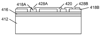
310에서, 발광 소자(416) 및 연관된 전극 컨택트들(418A, 418B)은 기판(412) 상에 생성되고, 일반적으로 성장 기판은 반도체 디바이스 및 상호접속층(interconnection layer)의 생성을 용이하게 한다. 발광 소자(416)는 층들의 스택(stack)으로서 도시되고, 애노드와 캐소드 사이의 발광 물질의 전형적인 삽입물(sandwich)에 대응한다. 임의의 수의 알려진 기술들을 이용하여 도 4a 및 4b의 구조체를 생성할 수 있으며, 도 4a는 측면도이고, 도 4b는 상면도이다.
본 예시적인 실시예에서, 디바이스는, 발광 소자(416)의 전극들(예컨대 애노드) 중 하나에 결합하기 위한 4개의 컨택트 영역들(418A)의 세트, 및 다른 전극(예컨대 캐소드)에 결합하기 위한 더 넓은 주변 영역(418B)을 제공하도록 구성된다. 갭(gap)(415)은 이 전극들(418A, 418B)을 분리한다. 4개의 컨택트 영역들(418A) 및 넓은 영역(418B)의 사용은 디바이스 내의 더욱 균일한 전류 밀도 분포를 용이하게 하고, 일부 실시예에서, 컨택트 영역들(418A)은 상이한 광출력 파장들(컬러들)을 제공하는 개별 발광 디바이스들에 결합될 수 있다. 참조의 편의를 위해, 여기서 이 전극들(418A)은 공통 전력원에 결합되도록 의도되는 것으로 상정된다.
320에서, 이하 상세히 기술된 대로 테스트는 상부 구조체의 생성 완료 후에 대안적으로 수행될 수 있어도, 생성된 발광 소자들(416)은 테스트될 수 있다. 330(도 4c)에서, 전극들을 선택 구역들(428A, 428B)에서는 제외하고, 후속 전도층들로부터 분리하기 위해, 유전체(dielectric)와 같은 절연 재료(420)가 구조체에 도포된다. 종래 리소그래픽(lithographic) 기술들은 이 패터닝된(patterned) 절연 재료(420) 층을 제공하기 위해 이용될 수 있다. 이하에 더 상세히 기술되듯이, 광출력은 전극들(418A, 418B) 및 절연체(420)로부터 멀어지는 방향으로 디바이스에서 나가도록 의도되고, 따라서, 전극들(418A, 418B) 및 절연층들(420)은 디바이스 내에 흡수되거나 손실된 광량을 감소시키도록 반사적인 것이 바람직하다. 대안적으로, 전극들(418A, 418B) 또는 절연층(420)은 투명할 수 있어, 후속 층들에 의존하여 그러한 반사를 제공할 수 있다. 또한 이하 더욱 상세히 기술된 대로, 절연체(420)는 바람직하게 열을 전도시키고, 전기를 전도시키지 않는다.
340(도 4d)에서, 상대적으로 키가 큰 절연/분리 디바이더(divider)들(430)은 구조체 상의 선택 구역들에 생성된다. 전형적인 실시예에서, 발광 소자(416)는 대략 5 마이크로미터 두께 정도일 수 있는 반면, 디바이더들(430)의 높이는 대략 100 마이크로미터 이상일 수 있다. 리소그래픽 기술은 선택 구역에서 경화되는 에폭시 수지(epoxy resin)와 같은 슬러리(slurry)를 사용하여, 이 디바이더들(430)을 생성하도록 사용될 수 있다. 디바이더들(430)이 직사각형 단면을 갖는 것처럼 도시되어 있지만, 당업자는 이 디바이더들(430)이 상부 면적보다 더 넓은 기저를 갖는 사다리꼴 형상을 가질 수 있음을 인지할 것이다.
350(도 4e)에서, 디바이더들(430) 사이의 공간들은 금속(438A, 438B)으로 채워진다. 구리와 같은 금속의 과도금(overplating)이 이어지는, 이 공간들 내의 시드층(seed layer)의 종래의 도포가 이용될 수 있다. 이 과도금은 의도적으로 디바이더들(430) 위로 확장될 수 있고, 이후 디바이더들(430)을 노출시키도록 기계적으로 또는 화학적으로, 또는 둘 다로 깎여서 영역들(438A, 438B)을 분리시킬 수 있다. 금속(438A)은 절연층(420) 내의 갭(들)(428A) 안으로 확장되어 그에 의해 발광 소자(416)의 전극 컨택트(들)(418A)에 접촉한다. 마찬가지로 금속(438B)은 갭(들)(428B) 안으로 확장되어 전극 컨택트(들)(418B)에 접촉한다.
360(도 4f)에서, 다른 절연층(442)이 선택 구역에 갭들(448A, 448B)을 갖고, 금속(438A, 438B) 위에 도포된다. 절연체(420)와 마찬가지로, 절연체(442)는 바람직하게 열을 전도시키고 전기를 전도시키지 않는다. 예컨대, 절연체(442)층은 SiO2 또는 Si3N4와 같은 무기 재료 또는 수지를 포함할 수 있다.
370(도 4f)에서, 최종 금속층은 절연층(442) 위에 도포된다. 이 예시에서, 3개의 전도성 컨택트들(444, 458A, 458B)이 형성된다. 컨택트(458A)에서의 금속은 갭(448A) 안으로 확장되어 금속(438A)을 통해 전극(418A)으로의 접촉을 제공하고, 컨택트(458B)에서의 금속은 갭(448B) 안으로 확장되어 금속(438B)을 통해 전극(418B)으로의 접촉을 제공한다. 이 컨택트들(458A, 458B)은 전력원을 발광 소자(416)에 결합하는 외부 컨택트들로서 역할을 한다. 당업자는 2개의 컨택트(458A, 458B)가 전술되고 이 도면들에 도시되어 있지만, 추가 컨택트들 또한 제공될 수 있음을 인지할 것이다. 예컨대, 발광 소자들(416)은 상이한 조명 레벨들, 상이한 컬러들 및 컬러들의 조합 등을 제공하기 위해 다수의 세그먼트들을 포함할 수 있다.
444에서의 금속 패드는 기저 금속 구조체들(438A, 438B)과 결합되지 않고, 열 방산을 위해 외부 접촉을 제공하는 역할을 한다. 즉, 절연층들(420, 442)을 통한 최소한의 단열을 상정하면, 금속 구조체들(438A, 438B)은 발광 소자(416)에 의해 생성된 열을 금속 패드(444)에, 그리고 거기로부터 인쇄 회로 기판과 같은 기저 기판에 전도하는 역할을 할 것이다.
380(도 4g-4h)에서, 구조체는 뒤집혀서, 코어 금속 구조체들(core metal structures)(438A, 438B)은 발광 디바이스에 대해 구조적 지지를 제공하여, 본래 성장 기판(412)이 제거되거나 두께가 감소되도록 하고, 그에 의해 광이 발광 소자(416)의 '상부'를 코어 금속 구조체들(438A, 438B)의 반대 방향으로 떠날 때, 광 손실을 감소시킨다. 도 4h의 하면도에 도시된 대로, 컨택트들(444, 458A, 458B)은 디바이스의 폭을 가로질러 확장될 수 있어, 디바이스로의 외부 접속들을 용이하게 할 수 있다.
특히, 본 발명의 원리를 이용하여 생성된 발광 디바이스는 웨이퍼 본딩을 요구하지 않고, 외부 컨택트들(458A, 458B)의 위치 및 배향은 내부 전극들(418A, 418B)의 위치 및 배향과 실질적으로 독립적이며, 그에 의해 스루-홀 비아들(도 2a 및 2b의 222)을 사용하는 것에 비해, 실질적인 설계 유연성을 제공한다.
도 4g의 구조체는 요구되는 대로 추가 처리될 수 있다. 예컨대, 백색 발광 디바이스를 생성하는 컬러들의 조합을 생성하기 위해, 예컨대 발광 소자(416)에 의해 생성된 컬러와 상이한 컬러(들)를 생성하는 파장 변환 물질(예컨대, 인광체)의 층이 도포될 수 있다. 마찬가지로, 특정 광학 특성을 제공하고/제공하거나 디바이스의 상부층들을 보호하기 위해 렌즈가 구조체 맨 위에 생성될 수 있다.
당업자는 도 4a-4h에 도시된 특정 구조체가 단지 예시적인 구조체임을 인지할 것이다. 도 5-8은 전술한 기술들을 이용하여 생성될 수 있는 몇몇 대안적인 구조체들을 도시한다. 참조의 편의를 위해, 이 도면들에서, 애노드 소자들은 밝은 음영으로 음영 처리되고, 캐소드 소자들은 중간 음영으로 음영 처리되고, 열 소자들은 어두운 음영으로 음영 처리된다. 절연 구역들은 음영 없이 도시된다.
도 5는 그 자체로는 분리된 열 소자를 갖지 않는 예시적인 구조체를 도시한다. 이 예에서, 벽(520)은 디바이스의 주변 둘레로 확장되고, 캐소드 구조체(528B)에 결합된다. 이 벽(520)은 디바이스의 외부 주변(outer perimeter)을 통해 열을 방산하도록 구성된다. 외부 열 싱크(sink) 또는 핀(fin) 구조체(도시되지 않음)는 열 방산을 더욱 용이하게 하기 위해 주변에 부착시킬 수 있다. 당업자는 벽(520)이 구조체들(528A, 528B)로부터 대안적으로 절연될 수 있고, 그에 의해 발광 소자(516)에 전기적으로 결합되지 않은 분리된 열 방산 소자를 형성함을 인지할 것이다.
도 6은 디바이스의 에지(edge)를 통해 애노드(528A) 및 캐소드(528B) 구조체들에 외부 접속을 제공하는 예시적인 구조체를 도시한다. 이 예에서, 열 소자(644)는 디바이스의 하부에 걸쳐 확장한다.
도 7은 인쇄 회로 기판(710)에 부착된 에지 접속 디바이스의 다른 예를 도시한다. 이 예에서, 캐소드 구조체(728B)만이 에지들로 확장되고, 애노드 구조체(728A)는 디바이스의 하부에서 컨택트(758A)로 확장된다. 캐소드(728B)는 솔더 조인트(solder joint)들(730)을 통해 인쇄 회로 기판(710) 상의 컨덕터들(712B)에 결합될 수 있고, 애노드 컨택트(758A)는 솔더 볼(solder ball)들(740)을 통해 인쇄 회로 기판(710) 상의 컨덕터(712A)에 결합될 수 있다. 솔더 볼들 또는 연속적인 솔더 필름(continuous solder film)의 사용을 포함하여, 구조체를 인쇄 회로 기판에 결합하는 다양한 결합 방법들이 이용될 수 있다.
도 8은 다수의 애노드 디바이스의 하면도를 도시한다. 전술한 대로, 발광 디바이스는 복수의 발광 소자들을 포함할 수 있다. 분리된 컨택트들(858A1-4)을 제공함으로써, 강도(intensity) 또는 컬러는 애노드들(858A1-4)의 하나 이상의 조합들을 선택적으로 활성화함으로써 변경될 수 있다. 당업자는 다양한 상이한 구성들을 용이하게 하도록 다수의 캐소드 컨택트들이 제공될 수 있음을 인지할지라도, 이 예에서는, 공통 캐소드 컨택트(858B)가 도시된다. 이 예에서 열 소자(844)는 애노드 및 캐소드 컨택트들 사이에 배치된다.
본 발명이 도면들과 전술한 설명에서 상세하게 도시되고 기술되었으나, 그러한 도시 및 기술은 제한적이 아닌, 설명적이거나 예시적인 것으로 간주되고, 본 발명은 개시된 실시예들에 제한되지 않는다.
개시된 실시예들에 대한 다른 변경들은, 청구된 발명을 실시함에 있어서, 도면들, 개시내용, 및 첨부된 청구항들의 연구(study)로부터 당업자에 의해 이해될 수 있고 달성될 수 있다. 청구항에서, "포함하는"이라는 단어는 다른 요소들 또는 단계들을 배제하지 않고, 부정관사 "a" 또는 "an"은 복수를 배제하지 않는다. 특정 방안들이 서로 상이한 종속 청구항들에서 언급된 점만으로, 이 방안들의 조합이 유리하게 사용될 수 없음을 나타내지는 않는다. 청구항 내의 임의의 참조 부호는 범위를 제한하는 것으로 이해되지 않아야 한다.
Claims (21)
- 발광 디바이스를 생성하는 방법으로서,
기판 상에 발광 구조체를 형성하는 단계 - 상기 발광 구조체는 상기 기판의 반대측에 상면을 갖고, 상기 상면에서 액세스 가능한 적어도 제1 및 제2 전극들을 포함함 -;
상기 전극들 위에 제1 절연층을 형성하는 단계 - 상기 제1 절연층은, 상기 제1 절연층 내에 상기 적어도 제1 및 제2 전극들에 각각 접촉하기 위한 적어도 제1 및 제2 개구부들을 가짐 -;
상기 제1 절연층 위에 절연 벽들을 형성하는 단계 - 상기 절연 벽들은 상기 적어도 제1 및 제2 개구부들 사이에 절연을 제공하도록 구성됨 -;
전기적 전도성 재료로 상기 절연 벽들 사이의 공간의 적어도 일부를 채우는 단계 - 상기 전기적 전도성 재료는 상기 적어도 제1 및 제2 전극들에 접촉하기 위해 상기 적어도 제1 및 제2 개구부들로 확장됨 -
상기 전기적 전도성 재료 위에 제2 절연층을 형성하는 단계 - 상기 제2 절연층은, 상기 적어도 제1 및 제2 개구부들 각각에서 확장되는 상기 전기적 전도성 재료의 적어도 하나의 부분에 접촉하기 위한 적어도 두 개의 추가 개구부를 가짐 -;
상기 제2 절연층 및 상기 적어도 두 개의 추가 개구부 상에 금속층을 도포(apply)하는 단계; 및
상기 제2 절연층의 상기 적어도 두 개의 추가 개구부를 통해 상기 전기적 전도성 재료의 상기 적어도 하나의 부분에 결합되는 적어도 두 개의 전기적 전도성 컨택트를 형성하는 단계
를 포함하고,
상기 절연 벽들과 상기 전기적 전도성 재료는 상기 발광 구조체에 구조적 지지를 제공하도록 구성되는 방법. - 제1항에 있어서,
상기 기판의 일부 또는 전부를 제거하는 단계를 포함하는 방법. - 삭제
- 제1항에 있어서,
상기 제2 절연층 및 상기 적어도 두 개의 추가 개구부 상에 금속층을 도포하는 상기 단계 후에, 상기 제2 절연층 상에 적어도 하나의 열 컨택트(thermal contact)를 형성하는 단계
를 포함하고,
상기 열 컨택트는 상기 전기적 전도성 재료로부터 전기적으로 절연되는 방법. - 제1항에 있어서,
상기 전기적 전도성 재료의 적어도 일부는 상기 발광 디바이스의 적어도 하나의 외부 에지로 확장되는 방법. - 제1항에 있어서,
상기 절연 벽들은 높이가 적어도 100 마이크로미터인 수지 벽들인 방법. - 제1항에 있어서,
상기 발광 구조체는 복수의 발광 소자들을 포함하는 방법. - 삭제
- 삭제
- 제1항에 있어서,
상기 제1 절연층의 반대 방향으로 상기 발광 구조체를 넘어 파장 변환층을 형성하는 단계를 포함하는 방법. - 제1항에 있어서,
상기 발광 구조체를 넘어 렌즈 소자를 형성하는 단계를 포함하는 방법. - 발광 디바이스로서,
적어도 제1 및 제2 전극들을 포함하는 발광 구조체;
의도된 광 출력 방향과 반대 방향으로의 상기 적어도 제1 및 제2 전극들 위의 제1 절연층 - 상기 제1 절연층은, 상기 제1 절연층 내에 상기 적어도 제1 및 제2 전극들에 각각 접촉하기 위한 적어도 제1 및 제2 개구부들을 가짐 -;
상기 제1 절연층 위의 하나 이상의 절연 벽들 - 상기 절연 벽들은 상기 적어도 제1 및 제2 개구부들 사이에 절연을 제공함 -;
상기 하나 이상의 절연 벽들 각각의 양쪽 측면 상에 배치된 전기적 전도성 재료 - 상기 전기적 전도성 재료는 상기 적어도 제1 및 제2 전극들에 접촉하기 위해 상기 적어도 제1 및 제2 개구부들로 확장됨 -;
상기 전기적 전도성 재료 위의, 상기 적어도 제1 및 제2 개구부들 각각에서 확장되는 상기 전기적 전도성 재료의 적어도 하나의 부분에 접촉하기 위한 적어도 두 개의 추가 개구부를 갖는 제2 절연층;
상기 제2 절연층 및 상기 적어도 두 개의 추가 개구부 상의 금속층; 및
상기 제2 절연층의 상기 적어도 두 개의 추가 개구부를 통해 상기 전기적 전도성 재료의 상기 적어도 하나의 부분에 결합되는 적어도 두 개의 전기적 전도성 컨택트
를 포함하고,
상기 절연 벽들과 상기 전기적 전도성 재료는 상기 발광 구조체에 구조적 지지를 제공하도록 구성되는 발광 디바이스. - 삭제
- 제12항에 있어서,
상기 제2 절연층 상의 적어도 하나의 열 컨택트를 포함하고,
상기 열 컨택트는 상기 전기적 전도성 재료로부터 전기적으로 절연되는 발광 디바이스. - 제12항에 있어서,
상기 전기적 전도성 재료의 적어도 일부는 상기 발광 디바이스의 적어도 하나의 외부 에지로 확장되는 발광 디바이스. - 제12항에 있어서,
상기 절연 벽들의 높이는 적어도 100 마이크로미터인 발광 디바이스. - 제12항에 있어서,
상기 발광 구조체는 복수의 발광 소자들을 포함하는 발광 디바이스. - 삭제
- 제12항에 있어서,
파장 변환층을 포함하는 발광 디바이스. - 제12항에 있어서,
렌즈 소자를 포함하는 발광 디바이스. - 삭제
Applications Claiming Priority (3)
| Application Number | Priority Date | Filing Date | Title |
|---|---|---|---|
| US201161435368P | 2011-01-24 | 2011-01-24 | |
| US61/435,368 | 2011-01-24 | ||
| PCT/IB2011/056010 WO2012101489A1 (en) | 2011-01-24 | 2011-12-29 | Light emitting device chip scale package |
Publications (2)
| Publication Number | Publication Date |
|---|---|
| KR20140004739A KR20140004739A (ko) | 2014-01-13 |
| KR101875247B1 true KR101875247B1 (ko) | 2018-07-05 |
Family
ID=45531903
Family Applications (1)
| Application Number | Title | Priority Date | Filing Date |
|---|---|---|---|
| KR1020137022350A KR101875247B1 (ko) | 2011-01-24 | 2011-12-29 | 발광 디바이스 및 그 생성 방법 |
Country Status (6)
| Country | Link |
|---|---|
| US (1) | US8951817B2 (ko) |
| EP (1) | EP2668675B1 (ko) |
| JP (1) | JP6110310B2 (ko) |
| KR (1) | KR101875247B1 (ko) |
| TW (1) | TWI553912B (ko) |
| WO (1) | WO2012101489A1 (ko) |
Cited By (1)
| Publication number | Priority date | Publication date | Assignee | Title |
|---|---|---|---|---|
| KR20220124421A (ko) * | 2021-03-03 | 2022-09-14 | 웨이브로드 주식회사 | 반도체 발광소자용 지지 기판 |
Families Citing this family (4)
| Publication number | Priority date | Publication date | Assignee | Title |
|---|---|---|---|---|
| DE102013100470A1 (de) * | 2013-01-17 | 2014-07-17 | Osram Opto Semiconductors Gmbh | Optoelektronischer Halbleiterchip |
| WO2014128574A1 (en) * | 2013-02-19 | 2014-08-28 | Koninklijke Philips N.V. | A light emitting die component formed by multilayer structures |
| KR102345751B1 (ko) | 2015-01-05 | 2022-01-03 | 삼성전자주식회사 | 반도체 발광소자 패키지 및 그 제조 방법 |
| KR102587215B1 (ko) * | 2016-12-21 | 2023-10-12 | 삼성디스플레이 주식회사 | 발광 장치 및 이를 구비한 표시 장치 |
Citations (2)
| Publication number | Priority date | Publication date | Assignee | Title |
|---|---|---|---|---|
| US20060278885A1 (en) * | 2005-06-14 | 2006-12-14 | Industrial Technology Research Institute | LED wafer-level chip scale packaging |
| JP2010141176A (ja) * | 2008-12-12 | 2010-06-24 | Toshiba Corp | 発光装置及びその製造方法 |
Family Cites Families (7)
| Publication number | Priority date | Publication date | Assignee | Title |
|---|---|---|---|---|
| JP2000244012A (ja) * | 1998-12-22 | 2000-09-08 | Toyoda Gosei Co Ltd | Iii族窒化物系化合物半導体素子の製造方法 |
| JP3589187B2 (ja) * | 2000-07-31 | 2004-11-17 | 日亜化学工業株式会社 | 発光装置の形成方法 |
| WO2006005062A2 (en) | 2004-06-30 | 2006-01-12 | Cree, Inc. | Chip-scale methods for packaging light emitting devices and chip-scale packaged light emitting devices |
| JP2010021261A (ja) * | 2008-07-09 | 2010-01-28 | Toshiba Corp | 光半導体素子の製造方法、光半導体素子及び光半導体装置の製造方法 |
| JP4799606B2 (ja) * | 2008-12-08 | 2011-10-26 | 株式会社東芝 | 光半導体装置及び光半導体装置の製造方法 |
| KR101047801B1 (ko) * | 2008-12-29 | 2011-07-07 | 엘지이노텍 주식회사 | 발광 디바이스 패키지 및 그 제조방법 |
| JP5759790B2 (ja) * | 2010-06-07 | 2015-08-05 | 株式会社東芝 | 半導体発光装置の製造方法 |
-
2011
- 2011-12-29 US US13/997,673 patent/US8951817B2/en active Active
- 2011-12-29 KR KR1020137022350A patent/KR101875247B1/ko active IP Right Grant
- 2011-12-29 JP JP2013549902A patent/JP6110310B2/ja active Active
- 2011-12-29 WO PCT/IB2011/056010 patent/WO2012101489A1/en active Application Filing
- 2011-12-29 EP EP11813570.6A patent/EP2668675B1/en active Active
-
2012
- 2012-01-20 TW TW101102646A patent/TWI553912B/zh active
Patent Citations (2)
| Publication number | Priority date | Publication date | Assignee | Title |
|---|---|---|---|---|
| US20060278885A1 (en) * | 2005-06-14 | 2006-12-14 | Industrial Technology Research Institute | LED wafer-level chip scale packaging |
| JP2010141176A (ja) * | 2008-12-12 | 2010-06-24 | Toshiba Corp | 発光装置及びその製造方法 |
Cited By (2)
| Publication number | Priority date | Publication date | Assignee | Title |
|---|---|---|---|---|
| KR20220124421A (ko) * | 2021-03-03 | 2022-09-14 | 웨이브로드 주식회사 | 반도체 발광소자용 지지 기판 |
| KR102457271B1 (ko) | 2021-03-03 | 2022-10-21 | 웨이브로드 주식회사 | 반도체 발광소자용 지지 기판을 제조하는 방법 |
Also Published As
| Publication number | Publication date |
|---|---|
| CN103314457A (zh) | 2013-09-18 |
| EP2668675A1 (en) | 2013-12-04 |
| JP2014503124A (ja) | 2014-02-06 |
| EP2668675B1 (en) | 2019-03-20 |
| TW201244182A (en) | 2012-11-01 |
| JP6110310B2 (ja) | 2017-04-05 |
| WO2012101489A1 (en) | 2012-08-02 |
| KR20140004739A (ko) | 2014-01-13 |
| US8951817B2 (en) | 2015-02-10 |
| TWI553912B (zh) | 2016-10-11 |
| US20130292716A1 (en) | 2013-11-07 |
Similar Documents
| Publication | Publication Date | Title |
|---|---|---|
| CN105826448B (zh) | 用于制造光电子半导体器件的方法和光电子半导体器件 | |
| US9431592B2 (en) | Submount with cavities and through vias for LED packaging | |
| JP5334966B2 (ja) | 光電構成素子の製造方法 | |
| TWI422044B (zh) | 封裝發光裝置之晶片尺度方法及經晶片尺度封裝之發光裝置 | |
| US7547923B2 (en) | Light emitting diode package having multi-stepped reflecting surface structure and fabrication method thereof | |
| US8120045B2 (en) | Metal-based photonic device package module | |
| US8399267B2 (en) | Methods for packaging light emitting devices and related microelectronic devices | |
| CN112736072B (zh) | 发光模组及其制造方法 | |
| KR101875247B1 (ko) | 발광 디바이스 및 그 생성 방법 | |
| US8936953B2 (en) | Light emitting diode thermally enhanced cavity package and method of manufacture | |
| KR101505336B1 (ko) | 갈바니 코팅된 광전자 반도체 소자 및 광전자 반도체 소자의 제조 방법 | |
| KR20150022868A (ko) | 광전자 모듈, 그리고 광전자 모듈의 제어 방법 | |
| US10546987B2 (en) | Method for producing a component, and a component | |
| TW201230416A (en) | Highly reflective coating on LED submount | |
| US20060145340A1 (en) | Substrate and method for fabricating the same | |
| WO2014184698A1 (en) | Chip scale light emitting device package in molded leadframe | |
| KR20180118551A (ko) | 라우팅 가능한 기판상에 제작된 디스플레이 패널 | |
| CN103314457B (zh) | 发光装置晶片级封装 | |
| KR101824177B1 (ko) | 리드프레임을 이용한 반도체 패키지 및 그 제조 방법 |
Legal Events
| Date | Code | Title | Description |
|---|---|---|---|
| A201 | Request for examination | ||
| E902 | Notification of reason for refusal | ||
| E701 | Decision to grant or registration of patent right |