KR100266297B1 - 표시장치 - Google Patents
표시장치 Download PDFInfo
- Publication number
- KR100266297B1 KR100266297B1 KR1019970058161A KR19970058161A KR100266297B1 KR 100266297 B1 KR100266297 B1 KR 100266297B1 KR 1019970058161 A KR1019970058161 A KR 1019970058161A KR 19970058161 A KR19970058161 A KR 19970058161A KR 100266297 B1 KR100266297 B1 KR 100266297B1
- Authority
- KR
- South Korea
- Prior art keywords
- panel
- display
- driving
- circuit
- area
- Prior art date
Links
Images



Classifications
-
- G—PHYSICS
- G02—OPTICS
- G02F—OPTICAL DEVICES OR ARRANGEMENTS FOR THE CONTROL OF LIGHT BY MODIFICATION OF THE OPTICAL PROPERTIES OF THE MEDIA OF THE ELEMENTS INVOLVED THEREIN; NON-LINEAR OPTICS; FREQUENCY-CHANGING OF LIGHT; OPTICAL LOGIC ELEMENTS; OPTICAL ANALOGUE/DIGITAL CONVERTERS
- G02F1/00—Devices or arrangements for the control of the intensity, colour, phase, polarisation or direction of light arriving from an independent light source, e.g. switching, gating or modulating; Non-linear optics
- G02F1/01—Devices or arrangements for the control of the intensity, colour, phase, polarisation or direction of light arriving from an independent light source, e.g. switching, gating or modulating; Non-linear optics for the control of the intensity, phase, polarisation or colour
- G02F1/13—Devices or arrangements for the control of the intensity, colour, phase, polarisation or direction of light arriving from an independent light source, e.g. switching, gating or modulating; Non-linear optics for the control of the intensity, phase, polarisation or colour based on liquid crystals, e.g. single liquid crystal display cells
- G02F1/133—Constructional arrangements; Operation of liquid crystal cells; Circuit arrangements
- G02F1/1333—Constructional arrangements; Manufacturing methods
- G02F1/1335—Structural association of cells with optical devices, e.g. polarisers or reflectors
- G02F1/1336—Illuminating devices
- G02F1/133602—Direct backlight
- G02F1/133603—Direct backlight with LEDs
-
- G—PHYSICS
- G09—EDUCATION; CRYPTOGRAPHY; DISPLAY; ADVERTISING; SEALS
- G09G—ARRANGEMENTS OR CIRCUITS FOR CONTROL OF INDICATING DEVICES USING STATIC MEANS TO PRESENT VARIABLE INFORMATION
- G09G3/00—Control arrangements or circuits, of interest only in connection with visual indicators other than cathode-ray tubes
- G09G3/20—Control arrangements or circuits, of interest only in connection with visual indicators other than cathode-ray tubes for presentation of an assembly of a number of characters, e.g. a page, by composing the assembly by combination of individual elements arranged in a matrix no fixed position being assigned to or needed to be assigned to the individual characters or partial characters
- G09G3/34—Control arrangements or circuits, of interest only in connection with visual indicators other than cathode-ray tubes for presentation of an assembly of a number of characters, e.g. a page, by composing the assembly by combination of individual elements arranged in a matrix no fixed position being assigned to or needed to be assigned to the individual characters or partial characters by control of light from an independent source
- G09G3/3406—Control of illumination source
-
- G—PHYSICS
- G09—EDUCATION; CRYPTOGRAPHY; DISPLAY; ADVERTISING; SEALS
- G09G—ARRANGEMENTS OR CIRCUITS FOR CONTROL OF INDICATING DEVICES USING STATIC MEANS TO PRESENT VARIABLE INFORMATION
- G09G2320/00—Control of display operating conditions
- G09G2320/02—Improving the quality of display appearance
- G09G2320/0233—Improving the luminance or brightness uniformity across the screen
-
- H—ELECTRICITY
- H05—ELECTRIC TECHNIQUES NOT OTHERWISE PROVIDED FOR
- H05K—PRINTED CIRCUITS; CASINGS OR CONSTRUCTIONAL DETAILS OF ELECTRIC APPARATUS; MANUFACTURE OF ASSEMBLAGES OF ELECTRICAL COMPONENTS
- H05K1/00—Printed circuits
- H05K1/02—Details
- H05K1/14—Structural association of two or more printed circuits
- H05K1/147—Structural association of two or more printed circuits at least one of the printed circuits being bent or folded, e.g. by using a flexible printed circuit
Landscapes
- Physics & Mathematics (AREA)
- Engineering & Computer Science (AREA)
- Nonlinear Science (AREA)
- General Physics & Mathematics (AREA)
- Chemical & Material Sciences (AREA)
- Mathematical Physics (AREA)
- Theoretical Computer Science (AREA)
- Crystallography & Structural Chemistry (AREA)
- Computer Hardware Design (AREA)
- Optics & Photonics (AREA)
- Devices For Indicating Variable Information By Combining Individual Elements (AREA)
- Electroluminescent Light Sources (AREA)
- Liquid Crystal (AREA)
Abstract
본 발명은 평면발광광원을 구비한 표시장치에 관한 것으로, 특히 그 평면발광광원으로서 EL패널을 구비한 표시장치에 관한 것으로서,
표시패널의 이면측이며 표시영역에 대응하는 부분에 일렉트로루미네센스·패널을 설치하고 표시패널의 표면측의 표시영역 이외의 영역에 표시패널의 구동회로를 설치하는 동시에 표시패널의 이면측의 상기 표시영역 이외의 영역에 대응하는 부분에 일렉트로루미네센스·패널의 구동회로인 인버터를 설치함으로써 표시장치의 소형박형화가 촉진되는 것을 특징으로 한다.
Description
본 발명은 평면발광광원을 구비한 표시장치에 관한 것으로, 특히 그 평면발광광원으로서 EL패널을 구비한 표시장치에 관한 것이다.
자기발광능력을 갖지 않는 표시장치인 액정표시장치에는 액정표시패널의 이면측에 평면발광형 백라이트로서 일렉트로루미네센스·패널(이하 EL패널이라 한다)을 구비한 것이 있다. 이 경우 EL패널 및 EL패널구동회로로서의 인버터는 액정표시패널과는 별개부품으로서 액정표시패널이 편입되는 제품에 탑재되어 있었다. 이 때문에 인버터회로를 제품의 머더보드(메인회로기판)에 탑재할 필요가 있었다.
그러나 이와 같은 종래의 EL패널을 백라이트로서 이용하는 액정표시장치를 제품의 표시장치로서 편입하는 경우 EL패널구동용 인버터가 별개부품으로서 머더보드에 탑재되기 때문에 액정표시장치가 편입되는 제품의 소형화 및 박형화를 촉진하는 것이 곤란해지는 문제가 있었다.
본 발명의 목적은 표시장치를 소형박형화하고, 이것이 편입되는 제품의 소형화 및 박형화를 대폭으로 촉진하는 것이다.
상기 목적을 달성하기 위해 본 발명의 표시장치는 소정의 표시영역을 갖고, 이 표시영역내에서 외부로부터 입사하는 빛의 투과를 제어하여 표시를 실시하는 표시패널과, 표시패널의 표면측이며 표시영역 이외의 영역에 설치된 표시패널을 구동하는 구동회로와, 표시패널의 이면측이며 상기 표시영역에 대응하는 부분에 설치되어 상기 표시영역에 빛을 조사하는 EL패널과, 표시패널의 이면측이며 표시영역 이외의 영역에 대응하는 부분에 설치되어 EL패널을 구동하는 구동회로를 구비한다.
상기한 바와 같이 구성된 표시장치에 따르면 표시패널의 이면측에 EL패널과 그 구동회로를 설치하여 표시장치로서 소형화, 또한 박형으로 유닛화할 수 있기 때문에 이 표시장치가 편입되는 예를 들면 휴대전화기 등의 제품의 소형화 및 박형화를 대폭으로 촉진할 수 있는 동시에 조립작업효율이 훨씬 향상한다.
상기한 표시장치에 있어서, EL패널을 구동하는 구동회로는 표시패널을 구동하는 구동회로와, 이 구동회로에 접속되는 배선회로가 설치된 영역의 이면측의 영역에 설치하는 것이 바람직하고, 이에 따라 표시장치가 소형화된다. 이 경우 적어도 표시패널을 구동하는 구동회로와 EL패널을 구동하는 구동회로의 사이에 접지접속한 도전성 시트를 개재시킴으로써 EL패널의 구동회로로부터 발생하는 노이즈가 표시패널의 구동회로에 영향을 미쳐서 표시불량이 발생하는 불합리가 확실하게 방지된다.
또 표시패널이 액정표시패널인 경우는 액정표시패널을 구동하는 구동회로를 표시영역외로 연장돌출시킨 한쪽의 기판상에 형성된 배선회로에 직접 탑재하는 것이 바람직하고, 그 경우의 배선회로가 형성되는 투명기판은 유리기판이어도 필름기판이어도 좋고, 유리기판의 경우는 COG실장법에 의해, 필름기판의 경우는 COF실장법에 의해 각각 직접 탑재된다.
또한 상기 표시장치에서는 표시패널의 표시영역이면 전체에 상기 EL패널의 발광영역이 접착제를 통하여 접착되어 있는 것이 바람직하고, 그 경우에 접착제 속에 적절한 안료를 분산혼합시킴으로써 EL패널의 출사광의 색을 소망하는 색으로 조정하여 표시패널에 입사시킬 수 있다.
또한 상기 표시장치에서는 표시패널의 구동회로와 EL패널의 구동회로가 공통의 입력배선회로와 접속되어 있는 것이 바람직하고, 그 경우의 공통의 입력배선회로는 가요성 배선회로(Flexible Printed Circuit)이면 실장면에서 보다 적합하게 된다.
또 상기 표시장치는 표시패널과 EL패널의 사이에 반투과반사막을 개재시키고 반투과반사형 표시장치로 할 수도 있다.
덧붙여서 상기 표시장치에 있어서, EL패널의 구동회로가 EL패널의 접속배선회로상에 직접 탑재되도록 해도 좋고, 그 경우 접속배선회로가 가요성 배선회로(Flexible Printed Circuit)인 것이 바람직하고, 이에 따라 표시장치의 소형박형화가 더욱 촉진된다.
또 상기 목적은 소정의 표시영역을 갖고, 이 표시영역내에서 외부로부터 입사하는 빛의 투과를 제어하여 표시를 실시하는 표시패널과, 표시패널의 표면측이며 표시영역 이외의 영역에 설치된 상기 표시패널을 구동하는 구동회로와, 표시패널의 이면측이며 표시영역에 대응하는 부분에 설치되어 상기 표시영역의 전체면에 걸쳐서 균일하게 빛을 조사하는 평면발광광원과, 표시패널의 이면측이며 표시영역 이외의 영역에 대응하는 부분에 설치되어 평면발광광원을 구동하는 구동회로를 구비하는 표시장치에 의해서도 달성된다.
이 표시장치에 의해서도 표시패널의 이면측에 평면발광광원과 그 구동회로를 설치하여 표시장치를 소형, 또한 박형으로 유닛화할 수 있기 때문에 이 표시장치가 편입되는 제품의 소형화 및 박형화를 대폭으로 촉진할 수 있는 동시에 조립작업효율이 훨씬 향상한다.
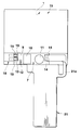
도 1은 본 발명의 한 실시예로서의 액정표시장치를 나타내는 평면도.
도 2는 도 1의 액정표시장치를 나타내는 배면도.
도 3은 도 1의 액정표시장치를 나타내는 분해측면도.
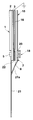
도 4는 도 1의 액정표시장치에 있어서의 일렉트로루미네센스·패널(이하 EL패널이라 한다)을 나타내는 평면도.
도 5는 도 4의 EL패널을 나타내는 배면도.
도 6은 도 4의 EL패널을 나타내는 측면도.
도 7은 도 4의 EL패널을 나타내는 측단면도.
도 8은 도 3에 나타내는 한 실시예의 변형예를 나타내는 분해측면도이다.
※도면의 주요부분에 대한 부호의 설명
1: 액정표시패널 2, 3: 투명기판
4: 돌출부 7: 인버터(EL패널구동회로)
8: 접착제 9: 인쇄회로기판
10: EL구동용 반도체칩 11: 인덕터
12: 콘덴서 15: EL패널
21: FPC필름
이하 첨부한 도면을 참조하여 본 발명의 실시예를 상세하게 설명한다.
도 1에 있어서, 이 액정표시장치는 액정표시패널(1)을 구비하고 있다. 이 액정표시패널(1)은 유리나 수지필름 등으로 이루어지는 2장의 투명기판(2, 3)간에 액정(도시하지 않음)이 봉입된 것으로 이루어져 있다. 이 경우 표면측의 투명기판(2)의 아래변으로부터 돌출된 이면측의 투명기판(3)의 돌출부(4)의 표면에 LSI칩 등으로 이루어지는 표시패널구동회로로서의 반도체칩(5)이 직접 탑재(COG 또는 COF실장)되어 있다.
액정표시패널(1)의 이면측이며 돌출부(4)에 대응하는 부분, 즉 돌출부(4)의 이면에는 도 2 및 도 3에 나타내는 바와 같이 인버터(EL패널구동회로)(7)가 접착제(8)를 통하여 접착되어 있다. 인버터(7)는 직류전력을 교류전력(200V 정도)으로 변환하는 장치로, 인쇄회로기판(9)의 상면에 EL구동용 반도체칩(10)과 인덕터(11)와 콘덴서(12)가 탑재된 구조로 되어 있다. 또 인쇄회로기판(9)의 일단부에는 후술하는 EL패널(15)과 접속되는 한쌍의 접속단자(13, 13)가 설치되고, 타단부에는 후술하는 FPC(Flexible Printed Circuit)필름(21)과 접속되는 한쌍의 접속단자(14, 14)가 설치되어 있다.
액정표시패널(1)의 이면측이며 표시영역(6)에 대응하는 부분에는 EL(Electro Luminescent)패널(15)이 접착제(16)를 통하여 접착되어 있다. 이 경우 EL패널(15)의 표면 전체가 액정표시패널(1)에 빛을 투과시키는 접착제(16)를 통하여 접착되어 있다. 또 본 실시예에서는 접착제(16) 속에 안료가 분산혼합되어 있다. 이 안료는 EL패널(15)로부터의 사출광의 색을 소망하는 색으로 조정하여 액정표시패널(1)에 입사시키기 위해 혼합하는 것이다.
도 4는 EL패널(15)의 평면도이고, 도 5는 EL패널(15)의 바닥면도이며, 도 6은 EL패널(15)의 측면도이고, 도 7은 EL패널(15)의 구성을 나타내는 측단면도이다. EL패널(15)은 예를 들면 PET(폴리에틸렌테레푸탈레이트) 등으로 이루어지는 투명한 가요성 필름기판(15a)의 이면에 ITO 등으로 이루어지는 투명전극(15b)이 설치되고, 투명전극(15b)의 이면에 형광체의 미분말을 유전체 속에 분산혼합시켜서 이루어지는 EL층(15c)이 설치되며, EL층(15c)의 이면에 카본 등으로 이루어지는 배면전극(15d)이 설치되고, 배면전극(15d)의 이면에 절연보호막(15e)이 설치된 구조로 되어 있다. 이 EL패널(15)은 표면에 이점쇄선으로 나타내는 발광영역(17)을 갖고 아래변오른쪽부에 접속부(18)가 설치된 구조로 되어 있다. 이 접속부(18)에는 투명전극(15b)과 배면전극(15d)이 인출되는 동시에 상기한 인버터(7)의 한쌍의 접속단자(13, 13)에 접속된 한쌍의 접속핀(19, 19)이 설치되어 있으며, 이들 한쌍의 접속핀(19, 19)과 투명전극(15b)과 배면전극(15d)의 인출단자부가 이방성 도전접착제(20)를 통하여 도전접속되어 있다.
도 1에 나타내는 바와 같이 액정표시패널(1)의 돌출부(4)의 표면에는 FPC필름(21)의 일단부가 접속되어 있다. 이 FPC필름(21)에는 도중에서 분기된 분기부분(21a)이 형성되어 있다. 이 분기부분(21a)의 선단부는 도 2에 나타내는 바와 같이 약 90도로 비틀어서 인버터(7)의 접속단자(14, 14)에 접속되어 있다.
이와 같이 본 실시예의 액정표시장치, 즉 액정표시패널과 백라이트 및 그들 구동회로를 포함한 액정표시모듈에서는 액정표시패널(1)의 이면측에서 표시영역(6)에 대응하는 부분에 백라이트로서 EL패널(15)을 부착하고, 액정표시패널(1)의 표시영역(6) 이외의 기판돌출부(4)의 이면측에 EL패널(15)의 구동회로인 인버터(7)를 설치하며, 액정표시패널(1)의 표면측에서 표시영역(6) 이외의 부분, 즉 투명기판(3)의 돌출부(4)표면측에 액정표시패널(1)의 구동회로인 반도체칩(5)을 직접 탑재하기 때문에 액정표시모듈 전체의 소형화 및 박형화가 대폭으로 촉진된다. 또 이 액정표시모듈에 따르면 EL패널구동용의 인버터(7)를 액정표시모듈과는 별개로 머더보드에 편입하는 종래의 경우에 비하여 EL패널부착 액정표시모듈의 실장작업이 매우 간단해지는 동시에 이 액정표시모듈이 편입되는 제품의 소형박형화가 크게 촉진된다.
또한 투명기판(2, 3)을 수지필름으로 형성하면 액정표시장치 전체를 더한층박형화할 수 있다.
또한 EL패널(15)의 표면 전체가 액정표시패널(1)에 접착제(16)를 통하여 접착되어 있기 때문에 EL패널(15)의 발광시에 발생하는 미소한 진동이 접착제에 의하여 흡수되어 이상음의 발생을 저감할 수 있다.
또 EL패널(15)을 액정표시패널(1) 이면에 접착해 있는 접착제(16) 속에 표시색조정을 위한 안료를 분산혼합하고 있기 때문에 EL패널(15)의 출사광의 색과는 다른 소망하는 표시색을 얻을 수 있다.
접착제와는 별개로 소망하는 표시색을 얻기 위한 색조정층으로서의 안료층을 도 7의 EL패널(15)에 있어서 가요성 필름기판(15a)의 표면 또는 그 이면에 형성한 투명전극(15b)상에 인쇄법 등에 의해 형성해도 좋다. 이 경우 안료층을 형성하는 영역을 부분적으로 선택하면 표시색을 부분적으로 다르게 할 수 있다. 또한 안료층을 복수장소에 선택적으로 형성하고, 각 안료층의 색을 서로 다르게 함으로써 표시색을 더욱 다양화할 수 있다. 덧붙여서 EL층(15c)에 안료를 직접 첨가하는 경우에는 경시변화에 따라서 색이 변화하는 일이 있는데, 상기한 바와 같이 안료를 접착제 속에 혼합시키거나 또는 필름기판(15a)상에 인쇄형성함으로써 표시색의 경시변화를 억제할 수 있다.
또한 상기 실시예에서는 인버터(7)의 인쇄회로기판(9)을 FPC필름(21)과는 별개체로 형성했지만, FPC필름과 일체로 형성해도 좋다. 이에 따라 부품점수를 저감할 수 있는 동시에 EL패널(15)과의 사이를 직접 접속할 수 있어서 접속핀(19)을 생략할 수 있다. 또한 그 FPC필름상에 인버터 등의 구동회로를 직접 탑재(COF)하면 실장이 보다 간소화되어 제품의 소형화가 더욱 촉진된다.
또 상기 실시예에서는 본 발명을 액정표시장치에 적용했지만, 이에 한정되지 않고 다른 표시장치에 적용할 수 있다.
또한 본 발명의 표시장치는 상기 실시예와 같이 항상 EL패널 등의 평면발광광원으로부터의 출사광으로 표시를 실시하는 투과형에 한정되는 것은 아니고 표시패널과 평면발광광원의 사이에 반투과반사막을 개재시키고, 밝은 곳에서는 평면발광광원을 소등하여 입사한 외광을 반투과반사막으로 반사시켜서 표시를 실시하고, 어두운 곳에서는 평면발광광원을 점등하여 이 출사광으로 표시를 실시하는 반투과반사형 표시장치로 할 수도 있다.
또한 본 발명은 표시패널의 광원으로서 EL패널 이외의 평면발광광원을 이용하는 경우, 예를 들면 도광판의 측부에 음극관을 배치한 광원유닛을 이용하는 경우에도 가장 적합하게 이용할 수 있다.
덧붙여서 표시패널구동회로와 평면발광광원의 구동회로의 사이에 접지접속한 도전성 시트를 설치해도 좋다. 예를 들면 도 8에 나타내는 상기 실시예의 변형예와 같이 액정표시패널(1)의 이면에 ITO 등의 투명도전성 시트(22)를 피착하고, 이 위에 접착제(8,16)를 통하여 EL패널(15) 및 이를 구동하는 인버터회로(7)를 탑재한 인쇄회로기판(9)을 접착할 수 있다. 이에 따라 평면발광광원의 구동회로로부터 발생되는 노이즈가 표시패널구동회로에 영향을 미쳐서 표시불량을 일으키는 불합리가 확실하게 방지된다. 또한 도 8의 변형예의 도전성 시트(22)는 액정표시패널(1)의 이면 전체면은 아니고 그 중의 EL패널(15)의 인쇄회로기판(9)이 접착되는 영역만에 피착하는 구성으로 해도 좋다.
Claims (8)
- 소정의 표시영역을 갖고 이 표시영역내에서 외부로부터 입사하는 빛의 투과를 제어하여 표시를 실시하는 표시채널과,상기 표시패널의 표면측이며 상기 표시영역 이외의 영역에 설치된 상기 표시패널을 구동하는 구동회로와,상기 표시패널의 이면측이며, 투명한 가요성 필름기판을 갖고, 상기 표시영역에 대응하는 부분에 접착제를 통하여 접착되며, 상기 표시영역에 빛을 조사하는 일렉트로루네센스·패널과,상기 표시패널의 이면측이며 상기 표시영역 이외의 영역에 대응하는 부분에 접착제를 통하여 접착된 일렉트로루미네센스·패널을 구동하는 구동회로를 구비하는 것을 특징으로 하는 표시장치.
- 제 1 항에 있어서,상기 일렉트로루미네센스·패널을 구동하는 구동회로가 상기 표시패널을 구동하는 구동회로와 해당 구동회로에 접속되는 배선회로가 설치된 영역의 이면측의 영역에 설치되고, 적어도 상기 일렉트로루미네센스·패널을 구동하는 구동회로와 상기 표시패널을 구동하는 구동회로의 사이에 접지접속된 도전성 시트가 상기 표시패널의 이면측에 피착되고, 해당 도전성 시트상에 상기 일렉트로루미네센스·패널을 구동하는 구동회로가 접착제를 통하여 접착되어 있는 것을 특징으로 하는 표시장치
- 제 1 항에 있어서,상기 표시패널은 한쌍의 투명기판간에 액정을 봉입하여 이루어지는 액정표시패널이며, 상기 투명기판은 가요성 수지필름기판, 또는 유리기판의 어느 쪽인가로 이루어지고, 상기 액정표시패널은 구동하는 구동회로가 상기 표시영역 이외의 영역으로 연장돌출시킨 한쪽의 투명기판상에 형성된 배선회로에 직접 탑재되는 것를 특징으로 하는 표시장치.
- 제 1 항에 있어서,상기 일렉트로루미네센스·패널을 상기 표시패널의 표시영역이면에 접착하는 상기 접착제 속에 안료가 분산혼합되어 있는 것을 특징으로 하는 표시장치.
- 제 1 항에 있어서,상기 표시패널의 구동회로와 상기 일렉트로루미네센스·패널의 구동회로가 공통의 입력배선회로와 접속되고, 상기 공통의 입력배선회로는 가요성 배선회로(Flexible Printed Circuit)인 것을 특징으로 하는 표시장치.
- 제 1 항에 있어서,상기 일렉츠로루미네센스·패널의 사이에 반투과막이 상기 표시채널의 이면측에 접착되고, 해당 반투과막에 접착제를 통하여 상기 일렉트로루미네센스·패널이 접착되어 있는 것을 특징으로 하는 표시장치.
- 제 1 항에 있어서,상기 일렉트로루미네센스·패널의 구동회로가 일렉트로루미네센스·패널의 접속배선회로상에 직접 탑재되고, 상기 접속배선회로가 가요성 배선회로(Flexible Printed Ciruit)인 것을 특징으로 하는 표시장치.
- 소정의 표시영역을 갖고, 이 표시영역내에서 외부로부터 입사하는 빛의 투과를 제어하는 표시를 실시하는 표시채널과,상기 표시채널의 표면측이며 상기 표시영역 이외의 영역에 설치된 상기 표시패널을 구동하는 구동회로와,상기 표시채널의 이면측이며 상기 표시영역에 대응하는 부분에 접착제를 통하여 접착되며, 상기 표시영역의 전체면에 걸쳐서 균일한 빛을 조사하는 평면광원과,상기 표시패널의 이면측이며 상기 표시영역 이외의 영역에 대응하는 부분에 접착제를 통하여 접착된 상기 평면광원을 구동하는 구동회로를 구비하는 것을 특징으로 하는 표시장치
Applications Claiming Priority (2)
| Application Number | Priority Date | Filing Date | Title |
|---|---|---|---|
| JP96-311226 | 1996-11-08 | ||
| JP8311226A JPH10143090A (ja) | 1996-11-08 | 1996-11-08 | 表示装置 |
Publications (2)
| Publication Number | Publication Date |
|---|---|
| KR19980042103A KR19980042103A (ko) | 1998-08-17 |
| KR100266297B1 true KR100266297B1 (ko) | 2000-09-15 |
Family
ID=18014620
Family Applications (1)
| Application Number | Title | Priority Date | Filing Date |
|---|---|---|---|
| KR1019970058161A KR100266297B1 (ko) | 1996-11-08 | 1997-11-05 | 표시장치 |
Country Status (7)
| Country | Link |
|---|---|
| JP (1) | JPH10143090A (ko) |
| KR (1) | KR100266297B1 (ko) |
| CN (1) | CN1165881C (ko) |
| HK (1) | HK1010934A1 (ko) |
| MY (1) | MY117919A (ko) |
| SG (1) | SG65696A1 (ko) |
| TW (1) | TW436749B (ko) |
Families Citing this family (6)
| Publication number | Priority date | Publication date | Assignee | Title |
|---|---|---|---|---|
| JP5020430B2 (ja) * | 1999-09-30 | 2012-09-05 | 京セラディスプレイ株式会社 | 液晶表示パネルの電極接続構造 |
| JP4491632B2 (ja) * | 2000-04-07 | 2010-06-30 | 日本電気株式会社 | 液晶表示装置の駆動方法 |
| KR100878217B1 (ko) * | 2001-08-28 | 2009-01-14 | 삼성전자주식회사 | 액정표시장치 및 이의 구동 방법 |
| KR20040003599A (ko) * | 2002-07-03 | 2004-01-13 | 주식회사 엘리아테크 | 유기 전계 발광 패널의 모듈 |
| JP5134523B2 (ja) * | 2008-12-17 | 2013-01-30 | 株式会社日立ハイテクノロジーズ | 光学フィルム貼付け装置、光学フィルム貼付け方法、および表示用パネルの製造方法 |
| CN103487968A (zh) * | 2013-09-22 | 2014-01-01 | 北京京东方光电科技有限公司 | 一种显示面板及显示器 |
-
1996
- 1996-11-08 JP JP8311226A patent/JPH10143090A/ja active Pending
-
1997
- 1997-11-04 MY MYPI97005235A patent/MY117919A/en unknown
- 1997-11-05 KR KR1019970058161A patent/KR100266297B1/ko not_active IP Right Cessation
- 1997-11-05 SG SG1997003959A patent/SG65696A1/en unknown
- 1997-11-06 TW TW086116535A patent/TW436749B/zh not_active IP Right Cessation
- 1997-11-07 CN CNB971216177A patent/CN1165881C/zh not_active Expired - Fee Related
-
1998
- 1998-11-16 HK HK98112047A patent/HK1010934A1/xx not_active IP Right Cessation
Also Published As
| Publication number | Publication date |
|---|---|
| JPH10143090A (ja) | 1998-05-29 |
| KR19980042103A (ko) | 1998-08-17 |
| MY117919A (en) | 2004-08-30 |
| CN1182256A (zh) | 1998-05-20 |
| CN1165881C (zh) | 2004-09-08 |
| TW436749B (en) | 2001-05-28 |
| SG65696A1 (en) | 1999-06-22 |
| HK1010934A1 (en) | 1999-07-02 |
Similar Documents
| Publication | Publication Date | Title |
|---|---|---|
| US5847783A (en) | LCD with electroluminescent panel drive circuitry mounted to oppose LCD drive circuitry | |
| KR100266160B1 (ko) | 일렉트로 루미네센스 패널부착 전자기기 | |
| EP0866264B1 (en) | Lighting device, liquid crystal display unit, and electronic equipment | |
| KR100786479B1 (ko) | 평판표시장치 및 이를 이용한 휴대용 표시기기 | |
| KR20090003932A (ko) | 연성 인쇄 회로 기판과 이를 이용한 액정 표시 장치 | |
| KR101129432B1 (ko) | 액정표시장치 | |
| KR20080024826A (ko) | 액정표시장치 | |
| US20070029915A1 (en) | Light-generating unit, display device having the same, and method of driving the same | |
| KR20200063125A (ko) | 백라이트 장치 | |
| KR20060126070A (ko) | 구동 집적 회로칩 패키지 및 이를 구비한 표시 장치 | |
| KR100266297B1 (ko) | 표시장치 | |
| KR20100091384A (ko) | 매립 직하형 엘이디 어레이 백라이트 유닛 및 그 제조방법 | |
| JP2005099619A (ja) | 電気光学装置、およびこの電気光学装置を備えた電子機器 | |
| US6198518B1 (en) | Liquid crystal display apparatus | |
| KR20070065079A (ko) | Led 램프 유닛, 이를 포함하는 백라이트 어셈블리 및이를 갖는 표시 장치 | |
| KR20080012511A (ko) | Led 유닛, 이를 이용한 백라이트 유닛 및 이를 구비하는표시 장치 | |
| JP2008129134A (ja) | 液晶表示装置およびそれを搭載する電子機器 | |
| KR200163007Y1 (ko) | 액정 디스플레이 모듈 | |
| KR20070054353A (ko) | 표시 장치 | |
| KR20060080766A (ko) | 백라이트 어셈블리 및 이를 이용한 표시장치 | |
| JPH10161113A (ja) | 表示装置 | |
| KR20070063242A (ko) | 표시 장치 | |
| KR100483530B1 (ko) | 인쇄회로기판 | |
| KR200232829Y1 (ko) | 양방향으로 발광하는 도광판 | |
| JPH08166588A (ja) | 液晶表示装置 |
Legal Events
| Date | Code | Title | Description |
|---|---|---|---|
| A201 | Request for examination | ||
| E902 | Notification of reason for refusal | ||
| E701 | Decision to grant or registration of patent right | ||
| GRNT | Written decision to grant | ||
| FPAY | Annual fee payment |
Payment date: 20130531 Year of fee payment: 14 |
|
| FPAY | Annual fee payment |
Payment date: 20140603 Year of fee payment: 15 |
|
| FPAY | Annual fee payment |
Payment date: 20150612 Year of fee payment: 16 |
|
| LAPS | Lapse due to unpaid annual fee |