JPWO2004088745A1 - Semiconductor device - Google Patents
Semiconductor device Download PDFInfo
- Publication number
- JPWO2004088745A1 JPWO2004088745A1 JP2004570148A JP2004570148A JPWO2004088745A1 JP WO2004088745 A1 JPWO2004088745 A1 JP WO2004088745A1 JP 2004570148 A JP2004570148 A JP 2004570148A JP 2004570148 A JP2004570148 A JP 2004570148A JP WO2004088745 A1 JPWO2004088745 A1 JP WO2004088745A1
- Authority
- JP
- Japan
- Prior art keywords
- layer
- wiring
- barrier metal
- copper
- metal layer
- Prior art date
- Legal status (The legal status is an assumption and is not a legal conclusion. Google has not performed a legal analysis and makes no representation as to the accuracy of the status listed.)
- Granted
Links
Images


Classifications
-
- H—ELECTRICITY
- H10—SEMICONDUCTOR DEVICES; ELECTRIC SOLID-STATE DEVICES NOT OTHERWISE PROVIDED FOR
- H10W—GENERIC PACKAGES, INTERCONNECTIONS, CONNECTORS OR OTHER CONSTRUCTIONAL DETAILS OF DEVICES COVERED BY CLASS H10
- H10W20/00—Interconnections in chips, wafers or substrates
- H10W20/01—Manufacture or treatment
- H10W20/031—Manufacture or treatment of conductive parts of the interconnections
- H10W20/056—Manufacture or treatment of conductive parts of the interconnections by filling conductive material into holes, grooves or trenches
-
- H—ELECTRICITY
- H10—SEMICONDUCTOR DEVICES; ELECTRIC SOLID-STATE DEVICES NOT OTHERWISE PROVIDED FOR
- H10W—GENERIC PACKAGES, INTERCONNECTIONS, CONNECTORS OR OTHER CONSTRUCTIONAL DETAILS OF DEVICES COVERED BY CLASS H10
- H10W20/00—Interconnections in chips, wafers or substrates
- H10W20/01—Manufacture or treatment
- H10W20/031—Manufacture or treatment of conductive parts of the interconnections
- H10W20/032—Manufacture or treatment of conductive parts of the interconnections of conductive barrier, adhesion or liner layers
- H10W20/033—Manufacture or treatment of conductive parts of the interconnections of conductive barrier, adhesion or liner layers in openings in dielectrics
- H10W20/036—Manufacture or treatment of conductive parts of the interconnections of conductive barrier, adhesion or liner layers in openings in dielectrics the barrier, adhesion or liner layers being within a main fill metal
-
- H—ELECTRICITY
- H10—SEMICONDUCTOR DEVICES; ELECTRIC SOLID-STATE DEVICES NOT OTHERWISE PROVIDED FOR
- H10W—GENERIC PACKAGES, INTERCONNECTIONS, CONNECTORS OR OTHER CONSTRUCTIONAL DETAILS OF DEVICES COVERED BY CLASS H10
- H10W20/00—Interconnections in chips, wafers or substrates
- H10W20/01—Manufacture or treatment
- H10W20/071—Manufacture or treatment of dielectric parts thereof
- H10W20/081—Manufacture or treatment of dielectric parts thereof by forming openings in the dielectric parts
- H10W20/083—Manufacture or treatment of dielectric parts thereof by forming openings in the dielectric parts the openings being via holes penetrating underlying conductors
-
- H—ELECTRICITY
- H10—SEMICONDUCTOR DEVICES; ELECTRIC SOLID-STATE DEVICES NOT OTHERWISE PROVIDED FOR
- H10W—GENERIC PACKAGES, INTERCONNECTIONS, CONNECTORS OR OTHER CONSTRUCTIONAL DETAILS OF DEVICES COVERED BY CLASS H10
- H10W20/00—Interconnections in chips, wafers or substrates
- H10W20/40—Interconnections external to wafers or substrates, e.g. back-end-of-line [BEOL] metallisations or vias connecting to gate electrodes
- H10W20/41—Interconnections external to wafers or substrates, e.g. back-end-of-line [BEOL] metallisations or vias connecting to gate electrodes characterised by their conductive parts
- H10W20/425—Barrier, adhesion or liner layers
Landscapes
- Internal Circuitry In Semiconductor Integrated Circuit Devices (AREA)
Abstract
銅配線におけるボイドの成長を抑制することのできる半導体装置を提供する。 半導体装置は、半導体基板と、前記半導体基板の上方に形成された絶縁層と、前記絶縁層に埋め込まれた第1ダマシン配線であって、底面および側面を画定し、内側に第1中空部を画定するバリアメタル層と、該第1中空部内に配置され、内側に第2中空部を画定する、銅配線層と、該第2中空部内に配置され、前記バリアメタル層とは分離されている補助バリアメタル層とを含む第1ダマシン配線と、前記第1ダマシン配線と絶縁層との上に配置された絶縁性銅拡散防止膜と、を有するを含む。Provided is a semiconductor device capable of suppressing the growth of voids in a copper wiring. The semiconductor device includes a semiconductor substrate, an insulating layer formed above the semiconductor substrate, and a first damascene wiring embedded in the insulating layer, defining a bottom surface and a side surface, and a first hollow portion inside. A barrier metal layer to be defined, a copper wiring layer disposed in the first hollow portion and defining a second hollow portion on the inside, and a barrier metal layer disposed in the second hollow portion and separated from the barrier metal layer A first damascene wiring including an auxiliary barrier metal layer; and an insulating copper diffusion prevention film disposed on the first damascene wiring and the insulating layer.
Description
本発明は、半導体装置に関し、特に銅ダマシン配線を有する半導体装置に関する。 The present invention relates to a semiconductor device, and more particularly to a semiconductor device having copper damascene wiring.
半導体集積回路装置は、集積度の向上と共に半導体素子及び配線が微細化し、さらなる多層配線が採用される。微細化された配線の高速動作を保証しようとすると、配線の抵抗を低減することが望まれる.アルミニウムに代って、より抵抗の低い銅が配線材料として用いられ始めている。銅配線を形成する場合、銅層を形成し、ホトリソグラフィを用いて微細にパターニングすることには限界がある。
微細化された銅配線を形成するために、ダマシンプロセスが採用される。絶縁層に配線用溝及び/又はビア孔を形成し、溝及び/又はビア孔を銅配線層で埋め込み、絶縁層上の余分な銅配線層を化学機械研磨(CMP)等により除去する。ダマシンプロセスにはシングルダマシンプロセスとデュアルダマシンプロセスがある。
シングルダマシンプロセスは、下層絶縁層を形成し、ビア孔を開口し、銅配線層で埋め込み、CMPで不要部を除去する。次に上層絶縁層を形成し、配線用溝を開口し、銅配線層で埋め込み、CMPで不要部を除去する。デュアルダマシンプロセスは、絶縁層を形成し、配線用溝とビア孔とを有する凹部を開口し、銅配線層で埋め込み、CMPで不要部を除去する。
銅は、絶縁層中に拡散し、絶縁層の絶縁特性を劣化させる性質を有する。このため、ダマシンプロセスで銅配線を形成する場合、先ず銅の拡散を防止する機能を有するバリアメタル層を形成し、その上に銅層を形成する。バリアメタルとしては、窒化チタンTiN,窒化タンタルTaN等の窒化物やタンタルTa等が用いられる。
CMPを行なった銅配線においても、表面に銅層が露出する。この銅層から上層の絶縁層へ銅が拡散することを防止するため、銅配線を形成した表面は、絶縁性銅拡散防止層で覆う。銅拡散防止層は、上層絶縁層をエッチングする時のエッチングストッパとしての機能も有する。絶縁性銅拡散防止層は、通常窒化シリコンSiNや炭化シリコンSiC等で形成される。
下部バリアメタル層を備えた銅配線を形成した後、配線層表面をエッチングして掘り下げ、上部バリアメタル層を形成し、CMPで不要部を除去する提案もされている(特許文献1)。この場合は、バリアメタル層で全周囲を覆われた銅配線が形成される。さらに、上部バリアメタル層に凹部を形成し、この中にアルミニウム層を埋め込んだ構成も提案されている(特許文献2)。
配線の高速性を保証するためには、配線周囲の絶縁層の実効誘電率を低くすることも望まれる。エッチストッパ兼銅拡散防止膜は、SiNやSiCで形成されるが、他の絶縁層はなるべく低い誘電率を持つ材料で形成することが配線の浮遊容量を低下させるためには好ましい。酸化シリコンより低い誘電率を有する絶縁材料は、それぞれ特有の性質を有する。各材料の特性を考慮した多層配線構造を形成することが望まれる。
A damascene process is employed to form miniaturized copper wiring. Wiring grooves and / or via holes are formed in the insulating layer, the grooves and / or via holes are filled with a copper wiring layer, and the excess copper wiring layer on the insulating layer is removed by chemical mechanical polishing (CMP) or the like. The damascene process includes a single damascene process and a dual damascene process.
In the single damascene process, a lower insulating layer is formed, a via hole is opened, it is filled with a copper wiring layer, and unnecessary portions are removed by CMP. Next, an upper insulating layer is formed, a wiring trench is opened, buried with a copper wiring layer, and unnecessary portions are removed by CMP. In the dual damascene process, an insulating layer is formed, a recess having a wiring trench and a via hole is opened, filled with a copper wiring layer, and unnecessary portions are removed by CMP.
Copper has the property of diffusing into the insulating layer and degrading the insulating properties of the insulating layer. For this reason, when forming a copper wiring by a damascene process, a barrier metal layer having a function of preventing copper diffusion is first formed, and a copper layer is formed thereon. As the barrier metal, a nitride such as titanium nitride TiN or tantalum nitride TaN, tantalum Ta, or the like is used.
Even in the copper wiring subjected to CMP, the copper layer is exposed on the surface. In order to prevent copper from diffusing from the copper layer to the upper insulating layer, the surface on which the copper wiring is formed is covered with an insulating copper diffusion preventing layer. The copper diffusion preventing layer also has a function as an etching stopper when the upper insulating layer is etched. The insulating copper diffusion preventing layer is usually formed of silicon nitride SiN, silicon carbide SiC, or the like.
There has also been proposed a method in which after forming a copper wiring having a lower barrier metal layer, the wiring layer surface is etched and dug to form an upper barrier metal layer, and unnecessary portions are removed by CMP (Patent Document 1). In this case, a copper wiring whose entire periphery is covered with a barrier metal layer is formed. Furthermore, a configuration in which a recess is formed in the upper barrier metal layer and an aluminum layer is embedded therein has been proposed (Patent Document 2).
In order to guarantee the high speed of the wiring, it is also desired to lower the effective dielectric constant of the insulating layer around the wiring. The etch stopper / copper diffusion prevention film is made of SiN or SiC, but the other insulating layers are preferably made of a material having a dielectric constant as low as possible in order to reduce the stray capacitance of the wiring. Each insulating material having a dielectric constant lower than that of silicon oxide has unique properties. It is desired to form a multilayer wiring structure considering the characteristics of each material.
本発明の目的は、長寿命化した銅配線を有する半導体装置を提供することである。
本発明の他の目的は、銅配線内におけるボイドの成長を抑制することのできる半導体装置を提供することである。
本発明の1観点によれば、半導体基板と、前記半導体基板の上方に形成された絶縁層と、前記絶縁層に埋め込まれた第1ダマシン配線であって、底面および側面を画定し、内側に第1中空部を画定するバリアメタル層と、該第1中空部内に配置され、内側に第2中空部を画定する、連続する銅配線層と、該第2中空部内に配置され、前記バリアメタル層とは分離されている補助バリアメタル層とを含む第1ダマシン配線と、前記第1ダマシン配線と絶縁層との上に配置された絶縁性銅拡散防止膜と、を有する半導体装置が提供される。
本発明の他の観点によれば、多数の半導体素子を形成した半導体基板と、前記半導体基板上に形成された積層絶縁層と、前記積層絶縁層中に埋め込まれた複数の下層配線層と複数の上層配線層とを含む多層配線であって、各配線層は、層内の接続を行うための配線パターンと層間の接続を行うためのビアとを有し、上層配線層の少なくとも1層は、前記積層絶縁層に埋め込まれた第1ダマシン配線であって、底面および側面を画定し、内側に第1中空部を画定するバリアメタル層と、該第1中空部内に配置され、内側に第2中空部を画定する、連続する銅配線層と、該第2中空部内に配置され、前記バリアメタル層とは分離されている補助バリアメタル層とを含む第1ダマシン配線を含んで構成される多層配線と、を有し、前記積層絶縁層は、各配線層の上に配置された絶縁性銅拡散防止膜を含む半導体集積回路装置が提供される。An object of the present invention is to provide a semiconductor device having a copper wiring with a long lifetime.
Another object of the present invention is to provide a semiconductor device capable of suppressing the growth of voids in a copper wiring.
According to one aspect of the present invention, a semiconductor substrate, an insulating layer formed above the semiconductor substrate, and a first damascene wiring embedded in the insulating layer, the bottom surface and side surfaces are defined, and A barrier metal layer that defines a first hollow portion; a continuous copper wiring layer that is disposed within the first hollow portion and defines a second hollow portion inside; and the barrier metal layer that is disposed within the second hollow portion, There is provided a semiconductor device including a first damascene wiring including an auxiliary barrier metal layer separated from a layer, and an insulating copper diffusion prevention film disposed on the first damascene wiring and the insulating layer. The
According to another aspect of the present invention, a semiconductor substrate on which a large number of semiconductor elements are formed, a laminated insulating layer formed on the semiconductor substrate, a plurality of lower wiring layers embedded in the laminated insulating layer, and a plurality of lower wiring layers Each of the wiring layers has a wiring pattern for connecting within the layer and a via for connecting between the layers, and at least one of the upper wiring layers is A first damascene wiring embedded in the laminated insulating layer, wherein the barrier metal layer defines a bottom surface and a side surface, defines a first hollow portion on the inside, and is disposed in the first hollow portion, and has a first inside. 2 includes a first damascene wiring including a continuous copper wiring layer defining a hollow portion and an auxiliary barrier metal layer disposed in the second hollow portion and separated from the barrier metal layer. Multi-layer wiring, and the laminated insulating layer The semiconductor integrated circuit device including a arranged insulating copper diffusion preventing film on the respective wiring layers are provided.
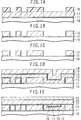
FIG.1A−1Eは、本発明の実施例による半導体装置の製造方法を示す断面図である。
FIG.2A−2Dは、本発明の他の実施例による半導体装置の製造法を示す断面図である。
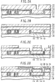
FIG.3A−3Cは、多層配線の積層絶縁層の例を示す断面図である。
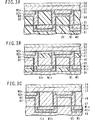
FIG.4A−4Cは、本発明の実施例によるビア導電体と下層配線層の接触部を示す断面図である。
FIG.5A、5Bは、本発明の他の実施例による半導体装置の断面図である。
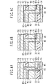
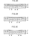
FIG.6A−6Cは、CMPの条件により発生し得る形態を示す断面図である。
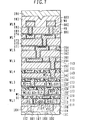
FIG.7は、多層配線を有する半導体装置の1例を示す断面図である。
FIG.8は、多層配線を有する半導体装置の他の1例を示す断面図である。
FIG.9A、9Bは、本発明者の行なった実験を示すスケッチ及び断面図である。FIG. 1A to 1E are cross-sectional views illustrating a method of manufacturing a semiconductor device according to an embodiment of the present invention.
FIG. 2A to 2D are cross-sectional views illustrating a method of manufacturing a semiconductor device according to another embodiment of the present invention.
FIG. 3A to 3C are cross-sectional views illustrating examples of the laminated insulating layer of the multilayer wiring.
FIG. 4A to 4C are cross-sectional views illustrating a contact portion between the via conductor and the lower wiring layer according to the embodiment of the present invention.
FIG. 5A and 5B are cross-sectional views of a semiconductor device according to another embodiment of the present invention.
FIG. 6A-6C are cross-sectional views showing forms that can occur depending on CMP conditions.
FIG. 7 is a cross-sectional view showing an example of a semiconductor device having a multilayer wiring.
FIG. 8 is a cross-sectional view showing another example of a semiconductor device having a multilayer wiring.
FIG. 9A and 9B are a sketch and a sectional view showing an experiment conducted by the present inventor.
アルミニウム配線において、電流によりアルミニウム原子がマイグレートするエレクトロマイグレーションが知られている。銅はアルミニウムよりエレクトロマイグレーションが生じにくいと言われている。しかし、銅配線においてもエレクトロマイグレーションは生じる。
先ず、本発明者の行なった予備的実験について説明する。本発明者は、デュアルダマシン配線を有するサンプルを作成し、加速試験を行ない、エレクトロマイグレーションによるボイドの発生を観察した。
FIG.9Aは、実験に用いたサンプルの透過型電子顕微鏡(TEM)写真のスケッチを示す。下層配線が、バリアメタル層B1と銅配線層W1で形成され、その端部に接触する上層配線層がバリアメタル層B2と銅配線層W2で形成されている。各配線の上面上には絶縁性銅拡散防止層が形成されている。この配線に電流を流した方向は、上層配線から下層配線に向って電子を供給する方向である。下層銅配線層W1には、上層配線との接触部に小さなボイドM1が発生し、配線の中間に大きなボイドM2が発生している。
FIG.9Bは、FIG.9Aの下層配線層の構成を概略的に示す断面図である。下層配線は、層間絶縁膜IL内に形成されている。下層銅配線層W1の表面上には、SiNで形成された絶縁性銅拡散防止層DBが配置されている。ボイドM1、M2は、下層銅配線層W1と、絶縁性銅拡散防止層DBとの界面に接して形成されている。
ボイドは、銅配線層と絶縁性銅拡散防止層との界面から発生していることが判る。バリアメタル層とその上に形成された銅配線層との界面には、ボイドは発生していない。
この実験結果から、バリアメタル層と銅配線層とは良好な界面を形成する、絶縁性銅拡散防止層と銅配線層とは良好な界面を形成できず、密着性が悪く、その界面における銅原子は移動し易く、界面拡散が生じやすくなっていると考えられる。絶縁性銅拡散防止層との界面において銅原子が界面拡散を始めると、空所に隣接する銅原子が体積移動し、体積移動する銅原子が不足するとボイドが発生し、成長すると考えられる。
なお、ボイドM1は、上層配線層のバリアメタル層B2と接する下層銅配線層W1内に発生しているが、バリアメタル層B2を介して隣接する上層銅配線層W2中には成長していない。このことは、銅配線層にボイドが発生すると、連続した銅配線層内においてはボイドが成長するが、バリアメタル層を突き抜けてボイドが成長することはないことを示唆している。
この現象を利用すると、ボイドの成長を抑制することが可能であろう。すなわち、銅配線層内にバリアメタル層を介在させると、バリアメタル層でボイドの成長を停止させることが可能であろう。
以下、本発明の実施例を図面を参照して説明する。
FIG.1A〜1Eは、本発明の第1の実施例による半導体装置の製造方法を概略的に示す。
FIG.1Aに示すように、半導体素子を含む下地10の上に、絶縁性銅拡散防止層11、層間絶縁層12の積層を形成する。銅拡散防止層11は、例えば厚さ50nmのSiN膜であり、層間絶縁層12は、例えば厚さ500nmの酸化シリコン層である。酸化シリコン層12の上に配線用溝の形状を有する開口を形成したホトレジストパターンPRを形成する。
ホトレジストパターンPRをエッチングマスクとし、酸化シリコン層12をエッチングする。窒化シリコン層11はエッチングストッパとして機能する。その後ホトレジストパターンPRはアッシング等により除去する。窒化シリコン層11下に銅配線等酸化しやすい要素が存在しても、窒化シリコン層11がその酸化を防止する。
FIG.1Bは、酸化シリコン層12をエッチングし、ホトレジストパターンPRを除去した状態を示す。開口内に窒化シリコン層11が露出している。この状態において、酸化シリコン層12をエッチングマスクとし、開口内に露出した窒化シリコン層11のエッチングを行なう。例えば、CF系ガス等を用いたプラズマにより窒化シリコン層11をエッチングする。
FIG.1Cは、窒化シリコン層11のエッチングが終了した状態を示す。酸化シリコン層12、窒化シリコン層11を貫通して配線用溝が形成されている。下地10内に、導電性プラグ等が形成されている場合は、酸化シリコン層12、窒化シリコン層11を貫通して形成された開口内に、これらの接続用領域が露出される。
FIG.1Dに示すように、配線用溝を形成した絶縁層上に、バリアメタル層13、銅配線層14を形成する。例えば、厚さ50nmのTa層をスパッタリングして、バリアメタル層13を形成し、シード用銅層をスパッタリングで形成した後銅層をメッキで形成して、厚さ約250nmの銅配線層14を形成する。厚さ50nmの窒化シリコン層11と厚さ500nmの酸化シリコン層12との積層で形成された深さ550nmの溝内に厚さ50nmのバリアメタル層13と厚さ250nmの銅配線層14が形成され、深さの半分以上が埋め戻される。溝の残る深さは250nmである。
メッキは、狭い開口部において優先的に成長するため、幅の狭い溝内は銅層14で埋め込まれる。広幅の配線層において、厚さ250nmの銅層14の表面は、厚さ500nmの酸化シリコン層12の表面よりも250nm下に配置される。
銅配線層14の上に、さらにバリアメタル層15を形成し、銅配線層16を成長する。例えば、厚さ50nmのTa層15をスパッタリングにより形成し、その後厚さ800nmの銅層16をメッキにより形成する。溝が550nmの深さを有しているので、銅配線層16の表面にも深さ約550nmの凹部が形成される。
FIG.1Dに示す状態で、CMPを行ない、酸化シリコン層14の上に堆積している銅層及びバリアメタル層を完全に除去する。CMPにおいて、研磨面と接する上面は機械研磨と化学研磨の両方を受ける。研磨面と接しない凹部内は化学研磨のみを受ける。このように、凹部内の研磨速度は遅いので、CMP途中において銅層16表面の凹凸は消滅し、平坦な表面が出現する。
FIG.1Eに示すように、酸化シリコン層12上の金属層を完全に除去し、銅層16表面を酸化シリコン層12表面と略同一平面として、CMPを終了する。酸化シリコン層12の表面が初めて露出した点でCMPを終了した場合、補助銅配線層の厚さは200nmとなる。オーバー研磨を行なうと、補助銅配線層の厚さは減少する。
平坦化された表面上に例えば窒化シリコン等の絶縁層銅拡散防止層17を成膜し、さらにその上に酸化シリコン層等の絶縁層18、窒化シリコン層等の保護層19を形成する。なお、さらに上層配線層を形成する場合には、保護層19の成長は省略する。
右側の広幅配線は、下からバリアメタル層13、銅配線層14、補助バリアメタル層15、補助銅配線層16の積層で形成される。絶縁性銅拡散防止層17は、配線の周辺部を除いた配線上面の主要部においては、補助銅配線層16に接し、銅配線層14には接しない。配線上面の周辺部の限られた面積のみにおいては、絶縁性銅拡散防止層17は、銅配線層14に接する。
補助銅配線層16内で銅原子のエレクトロマイグレーションによりボイドが発生しても、そのボイドは補助バリアメタル層15によって閉じ込められるであろう。
銅配線層14は、周辺の限られた面積で絶縁性銅拡散防止層17と接するが、上下主要部をバリアメタル層13、15で挟まれた構成のため、ボイドが発生しにくい。ボイドの発生に基づく不良の発生を抑制することが可能となり、太幅配線における電流密度を増大することも可能となる。
FIG.9Cは、期待される機能を示す概略断面図である。層間絶縁膜IL内にバリアメタル層B1、銅配線層W1、補助バリアメタル層B1x、補助銅配線層W1xで構成された配線パターンが形成されている。配線パターンの1端には、バリアメタル層B2、銅配線層W2で構成された上層配線のビアが接続されている。配線パターン上面上には銅拡散防止層DBが形成されている。
銅拡散防止層DBと補助銅配線層W1xとの界面で銅原子の界面拡散が生じ、それに伴って銅原子の体積移動が生じ、ボイドMが発生する。ボイドMは成長するが、補助バリアメタル層B1xで成長は停止する。下部に配置された銅配線層W1中にボイドが成長することは抑止される。
FIG.1A−1Eに示した実施例においては、細幅の配線層には補助バリアメタル層15は配置されず、太幅の配線層にのみ補助バリアメタル層15が形成され、その上に補助銅配線層16が形成された。細幅配線においてボイドが発生すると不良が生じてしまう。製造条件を調整することにより、細幅配線にも補助バリアメタル層を配置することもできる。
FIG.2A−2Dは、本発明の第2の実施例による半導体装置の製造方法を示す。FIG.1A−1Cと同様の工程を行ない、絶縁性銅拡散防止層11、層間絶縁層12に配線用溝を形成する。
FIG,2Aに示すように、配線用溝を形成した半導体基板表面上にバリアメタル層13を成膜した後、銅配線層14を化学気相堆積(CVD)により形成する。CVDは、等方成長を行なうため、バリアメタル層13表面上に均一な厚さの銅配線層14が形成される。太幅配線溝内のみならず、細幅配線溝内においても、中空部が残るように銅配線層14の厚さを選択する。
銅配線層14の上に、補助バリアメタル層15を形成し、さらに補助銅配線層16を形成する。その後CMPを行ない、酸化シリコン層12上の金属層を全て除去する。
FIG.2Bに示すように、太幅配線溝内のみでなく、細幅配線溝内においても、補助バリアメタル層15、補助配線層16が埋め込まれた配線が形成される。第2の実施例によれば、銅配線層14の厚さが均一にかつ薄く設定され、細幅配線内においても補助バリアメタル層15、補助銅配線層16が形成される。細幅配線、太幅配線を問わず、ボイドを原因とする配線の断線を減少することができる。以下、上層にデュアルダマシン配線を形成する工程を説明する。
CMPした表面上に、窒化シリコン層等の絶縁性銅拡散防止層21、酸化シリコン等の絶縁層22、窒化シリコン等のエッチストッパ層23、酸化シリコン等の絶縁層24を成長する。これらの絶縁積層は、合わせて配線層1層分の層間絶縁膜を構成する。窒化シリコン層23、酸化シリコン層24が配線パターン用絶縁層である。
FIG.2Cに示すように、絶縁層23、24に配線パターン用溝、絶縁層22、21にビア孔を形成し、デュアルダマシン用凹部を形成する。デュアルダマシン用凹部を形成する方法としては、先にビア孔を形成し、後に配線パターン用溝を形成する公知の方法、先に配線パターン用溝を形成し、後にビア孔を形成する公知の方法のいずれを用いてもよい。
FIG.2Dに示すように、デュアルダマシン用凹部を埋め込むように、バリアメタル層25、銅配線層26、補助バリアメタル層27、補助銅配線層28を形成し、CMPを行なって絶縁積層表面上の金属層を除去し、デュアルダマシン配線を完成する。
ビア孔の径は通常細く設計されるので、ビア孔内は、バリアメタル層25と銅配線層26、又はバリアメタル層25のみで埋め込まれる。ビア導電体は絶縁性銅拡散防止膜に接しないので補助バリアメタル層25がビア導電体に含まれなくても実質的な不利は生じない。補助バリアメタル層27、補助銅配線層28は、配線パターン内にのみ形成される。
FIG.1E、2Dの構成によれば、配線の主要部において、絶縁性銅拡散防止層17、21は、補助銅配線層16とは接触するが、配線層13とは補助バリアメタル層で分離され、接触していない。絶縁性銅拡散防止層17,21との界面において、補助銅配線層16内に界面拡散が生じ、ボイドが発生しても、そのボイドは補助銅配線層16内にあり、補助バリアメタル層15によって成長を止められ、配線層13に拡がることは防止される。
補助銅配線層は、ボイドの発生、成長を許容する領域である。補助銅配線層から補助バリアメタル層を介して分離されている銅配線層は、銅拡散防止層との接触が周辺部のみに制限され、ボイドの発生を抑制した領域である。
補助銅配線層の銅配線層に対する体積比が小さいほど、ボイドの発生を抑制した銅配線の断面積が大きくなる。この観点からは、補助バリアメタル層、補助銅配線層は、浅く、例えば配線溝の深さの1/2以下の深さに、形成することが好ましい。第1の実施例のように、太幅配線のみを対象として補助バリアメタル層、補助銅配線層を形成すれば、その厚さを制限することが容易となる。
上述の実施例においては、絶縁性銅拡散防止層、及びエッチングストッパ層としてSiNを用い、絶縁層としては酸化シリコンを用いた。種々の他の絶縁層を用いることも可能である。
FIG.3A、3B、3Cは、種々の材料を用いた絶縁積層構造の例を示す。
FIG.3Aにおいては、SiLK(ダウケミカル社商標)等の有機絶縁層31の上に、SiCのハードマスク層32を重ね、下層配線の層間絶縁層が形成されている。この層間絶縁層内に、バリアメタル層B1、銅配線層W1、補助バリアメタルB1x、補助銅配線層W1xで形成された銅配線パターンが埋め込まれている。銅配線パターンは実施例1、2のいずれかのものでよい。
銅配線パターンの上には、SiCの銅拡散防止層兼エッチングストッパ層33、有機絶縁層34、SiCのハードマスク層35が積層され、上層配線の層間絶縁膜を形成している。これらの層間絶縁膜を貫通して、ビア部とを配線部を有するデュアルダマシン上層配線が、バリアメタル層B2、銅配線層W2、補助バリアメタル層B2x、補助銅配線層W2xで形成されている。
上層配線の上には、SiCの銅拡散防止層52、SiO2等の絶縁層53、SiN等の保護層54が形成されている。
FIG.3Bにおいては、酸化シリコン層36、有機絶縁層37、酸化シリコン層38で下層配線用の層間絶縁膜が形成されている。この積層絶縁層内に、上述同様の下層銅配線が埋め込まれている。
上層配線用の層間絶縁膜は、SiN等の銅拡散防止層39、酸化シリコン層40、有機絶縁層41、酸化シリコン層42で構成されている。この積層絶縁層内に、上述同様のデュアルダマシン上層配線が埋め込まれている。
この層間絶縁膜構造は、有機絶縁膜を用いて実質誘電率を低減させながら、有機絶縁膜を酸化シリコン層で挟むことにより、プロセス上の安全性を高めている。上層配線より上の絶縁膜はFIG.3A同様の構成を有する。有機絶縁膜と酸化シリコン膜とは、異なるエッチング特性を有する。この特性の差を利用してエッチングをより容易に制御することができる。
FIG.3Cにおいては、弗化酸化シリコン(SiOF、またはFSG)層46が下層配線の層間絶縁膜を構成する。この絶縁層内に、上述同様の下層銅配線が埋め込まれている。SiN等の絶縁性銅拡散防止層47と、弗化酸化シリコン層48が上層配線の層間絶縁膜を構成している。この積層絶縁層内に、上述同様のデュアルダマシン上層配線が埋め込まれている。
なお、バリアメタル層としては、Ta、TiN、TaN等を用いることができる。但し、弗化酸化シリコンを用いたFIG.3Cの構成においては、弗化酸化シリコン層の上に配置されるバリアメタル層B1及びB2としては、Ta以外のTiN、TaNを用いることが好ましい。
FIG.4A、4B、4Cは、下層配線と上層配線の接続部の形状を、FIG.3Bに示す構造を例として、示す。FIG.3Bと同様の符号は同様の部材を示す。
FIG.4Aにおいては、上層配線のビア部B2,W2は下層配線のバリアメタル層B1から、銅配線層W1、補助バリアメタル層B1x、補助銅配線層W1xにわたる領域でコンタクトを形成している。この構成は、FIG.3Bで示したものと同様である。上層配線のビア部は、銅配線層W1のみでなく補助銅配線層W1xとも接触している。
FIG.4Bにおいては、下層配線のバリアメタル層B1、銅配線層W1及び補助バリアメタル層B1xの上面のみにおいて、上層配線のビア部が接触を形成している。上層配線のビア部B2,W2は、銅配線層W1とは接触するが、補助銅配線W1xには接触していない。
FIG.4Cにおいては、下層配線のバリアメタル層B1、銅配線層W1の上面にのみ、上層配線のビア部B2,W2が接触を形成している。上層配線のビア部B2,W2は、銅配線層W1を横断せず、補助バリアメタル層B1xとの間に銅配線層W1と銅拡散防止層39とが接触する領域がある。
これらのコンタクト構造は、条件、必要に応じて選択することができる。
FIG.5Aは、ビア部と配線パターン部とを別々のプロセスで形成するシングルダマシン構造による半導体装置の構成例を示す。下地絶縁層60の上に、SiN等のエッチングストッパ層61、酸化シリコン層62を形成し、下層配線の層間絶縁膜を構成する。この層間絶縁膜中に、バリアメタル層63、銅配線層64、補助バリアメタル層65、補助銅配線層66で形成された下層配線パターンが埋め込まれている。
下層配線層の上に、エッチングスストッパ層67、酸化シリコン層68が積層され、上層配線のビア部が埋め込まれている。ビア部は、バリアメタル層69、銅配線層70のみで構成されている。ビア部の上に、エッチングストッパ層11、酸化シリコン層12で配線パターン用絶縁層が形成され、この中にバリアメタル13、銅配線層14、補助バリアメタル層15、補助銅配線層16で形成された配線パターンが埋め込まれている。
この配線パターンの上面を、SiN等のエッチングストッパ17が覆い、さらに酸化シリコン層18が形成され、さらに上層配線のバリアメタル層71、銅配線層72で形成されたビア部が接触する。
シングルダマシン構造においては、ビア部の銅配線層70は、配線パターンのバリアメタル層13で覆われ、銅拡散防止層(エッチングストッパ層)11、17とは接触しない。銅拡散防止層17と接触する配線パターンの銅配線層14とビア部の銅配線層70とはバリアメタル層13で分離される構造である。従って、ビア部に補助バリアメタル層を設ける必要は少ない。
FIG.5Bは、配線パターンの構造の変形例を示す。下地絶縁層40の上に、例えば有機絶縁層41と酸化シリコン層42とで層間絶縁膜が形成されている。この層間絶縁膜中に、バリアメタル層B、銅配線層W、補助バリアメタル層Bxで形成された配線パターンが埋め込まれている。この上に、絶縁性銅拡散防止層が形成される。補助バリアメタル層はバリアメタル層と分離されている。
この構成においては、補助バリアメタル層Bxの上に補助銅配線層は配置されていない。銅配線層Wの主要部上に補助バリアメタル層Bxが形成されているため、銅配線層Wと絶縁性銅拡散防止層との接触が制限され、ボイドの発生が抑制される。補助バリアメタル層Bxの厚さは、CMPで消滅しないように選択することが好ましい。
FIG.6A、6B、6Cは、広幅配線においてディッシング及びエロージョンが生じた時の構成の変化を示す。
FIG.6Aにおいて、酸化シリコン層40、有機絶縁層41、酸化シリコン層42で形成される絶縁積層構造に、第1、第2実施例のいずれかと同様バリアメタル層B、銅配線層W、補助バリアメタル層Bx、補助銅配線層Wxで形成された配線パターンが埋め込まれている。配線パターン形成の際のCMPにおいて、ディッシング及びエロージョンが生じると、配線パターン上面が、中央部に向って次第に引き下げられた形状となる。
FIG.6Bは、ディッシング及びエロージョンがさらに強い場合を示す。配線層の上面は、中央部で補助バリアメタル層Bxに達している。この状態においても、銅配線層Wの主要部は絶縁性銅拡散防止層とは接触しないのでボイドの発生は抑制される。第1、第2実施例のいずれかと図5Bの実施例との組み合わせを考えることもできるであろう。
FIG.6Cは、さらにディッシング及びエロージョンが強くなった場合を示す。補助バリアメタル層Bx及び補助銅配線層Wxの中央部は、ディッシング及びエロージョンにより消滅し、銅配線層Wが露出している。絶縁性銅拡散防止層は、銅配線層Wの露出部と接触する。
この状態においても、補助バリアメタル層Bxが残っている領域においては、銅配線層Wと絶縁性銅拡散防止層との接触が防止されているため、ボイドの発生は抑制される。
FIG.7は、多層配線構造を有する半導体集積回路装置の構成例を示す。シリコン基板101に、シャロートレンチアイソレーション(STI)による素子分離領域102が形成されている。素子分離領域102で囲まれた活性領域内にMOSトランジスタを形成するため、p型ウエル103、n型ウエル104が形成されている。
p型ウエル領域103上に、ゲート絶縁膜105、多結晶シリコンゲート電極106、サイドウォールスペーサ107が形成され、ゲート電極106の両側にエクステンション付n型ソース/ドレイン領域108が形成される。n型ウエル領域104においては、p型ソース/ドレイン領域109が形成される。
ゲート電極を覆って半導体基板上に窒化シリコン層111が形成され、その上にホスホシリケートガラス(PSG、燐ドープ酸化シリコン)層112が形成される。PSG層112、窒化シリコン層111を貫通して、TiNのバリアメタル層B11とタングステン層V1とで形成されたビア導電体が形成される。
PSG層112の上に、有機絶縁層113、酸化シリコン層114が積層される。この積層の中に、バリアメタル層B1、銅配線層W1、補助バリアメタル層B1x、補助銅配線層W1xで形成された配線パターンが埋め込まれる。このようにして第1配線層WL1が形成される。
第1配線層WL1の上に、窒化シリコン層121、酸化シリコン層122、有機絶縁層123、酸化シリコン層124の積層が形成され、第2配線WL2用の層間絶縁膜が形成される。第2配線用層間絶縁膜に、バリアメタル層B2、銅配線層W2、補助バリアメタル層B2x、補助銅配線層W2xで形成された第2配線層WL2が埋め込まれる。
第3配線層WL3、第4配線層WL4用の層間絶縁膜は、第2配線WL2に対する層間絶縁膜と同様、窒化シリコン層131、141、酸化シリコン層132、142、有機絶縁層133、143、酸化シリコン層134、144の積層で形成される。
第3配線層WL3、第4配線層WL4のダマシン配線の構造は、第2配線層と同様である。バリアメタル層Bn、銅配線層Wn、補助バリアメタル層Bnx、補助銅配線層Wnxで配線パターンが形成される。
第5配線層WL5〜第7配線層WL7は、第2配線層WL2〜第4配線層WL4とは異なる構成を有する。第5配線層WL5の層間絶縁膜は、窒化シリコン層151、酸化シリコン層152、窒化シリコン層153、酸化シリコン層154の積層で形成されている。配線パターンの構成は、第2〜第4配線WL4と同様である。
第6配線層、第7配線層に対する層間絶縁膜も、第5配線層WL5同様窒化シリコン層161、171、酸化シリコン層162、172、窒化シリコン層163、173、酸化シリコン層164、174で形成されている。配線パターンの構成は、第5配線WL5と同様である。
上層配線は、配線間ピッチが広くなり、配線密度が緩やかになる。このため、配線間の浮遊容量を低減するため、低誘電率絶縁層を用いる必要性が低くなる。そこで、第5〜第7配線層では、有機絶縁層を用いず、層間絶縁層の信頼性を高めている。
最上層の第8配線層WL8は、独自の構成を有する。窒化シリコン層181、酸化シリコン層182で下部絶縁層が形成され、バリアメタル層B81、タングステン層V8でビア部が形成される。
ビア部の上に、TiN層B82、アルミニウム層W8、TiN層B83でパッド兼用の配線層が形成されている。なお、アルミニウムの代りにCuを用いることもできる。最上層の配線を覆って、酸化シリコン層183、窒化シリコン層190が形成されている。
FIG.7の構成においては、第1配線層WL1〜第7配線層WL7の全てにおいて配線パターン中に補助バリアメタル層を埋め込み、ボイドの発生を抑制している。層間絶縁膜の構成は、下部配線層と最上層を除く上部配線層でその構成が異なっている。
FIG.8は、多層配線構造を有する半導体集積回路装置の他の構成例を示す。半導体基板内に形成するMOSトランジスタ構造及びソース/ドレインの引出し導電性プラグの構成は、FIG.7と同様である。
PSG層112の上に、SiC層116、有機絶縁層117、SiC層118の積層が形成され、バリアメタル層B1、銅配線層W1で第1配線層WL1が形成されている。補助バリアメタル層は用いられていない。
第2配線層WL2〜第4配線層WL4は、第1配線層WL1と同様の構成を有する。第4配線層WL4を例にとって説明すると、層間絶縁膜はSiC層141、有機絶縁層142、SiC層143で形成されている。デュアルダマシン配線は、バリアメタル層B4と銅層W4で形成され、補助バリアメタル層は配置されていない。
第5配線層WL5〜第8配線層WL8はそれぞれ同様の構成を有する。第5配線層WL5を例にとって説明すると、層間絶縁膜は、SiC層151、酸化炭化シリコン(SiOC)層152、SiC層153、酸化炭化シリコン層154で形成されている。デュアルダマシン配線は、バリアメタル層Bおよび銅配線層Wで形成され、補助バリアメタル層は配置されていない。
第9配線層WL9は、SiC層191、酸化シリコン層192、SiC層193、酸化シリコン層194で形成された層間絶縁膜に、バリアメタル層B9、銅配線層W9、補助バリアメタル層B9x、補助銅配線層W9xで形成されたデュアルダマシン配線が埋め込まれる。
第10配線WL10は、第9配線WL9と同様の構成を有する。SiC層201、酸化シリコン層202、SiC層203、酸化シリコン層204で形成されて層間絶縁膜にバリアメタル層B10、銅配線層W10、補助バリアメタル層B10x、補助銅配線層W10xで形成されたデュアルダマシン配線が埋め込まれる。
最上配線層WL11は、FIG.7の最上配線と同様の構成を有する。SiC層211、酸化シリコン層212が積層され、この中にTiNのバリアメタル層B11と、Wの配線層W11で形成されたビア導電体が埋め込まれている。ビア導電体の上に、TiN層B111、アルミニウム、又は銅を含むアルミニウム合金で形成された主配線層W12、TiNの上部バリアメタル層B112で形成されたボンディングパッド兼用最上配線層が形成される。この配線層を覆って、酸化シリコン層213、窒化シリコン層220が形成される。
FIG.8の構成においては、下層から上層に向って3段階で層間絶縁層の積層構成が変化し、実質的誘電率は下層ほど低くされている。下層配線は高密度であり、配線の付随容量を低減するためには層間絶縁層の誘電率を低減することが好ましい。
下層配線層、中層配線層には補助バリアメタル層、補助銅配線層が配置されず、上層の2層の配線層WL9、WL10にのみ、補助バリアメタル層、補助銅配線層を配置している。上層配線層は、電源配線の占める割合が高く、大電流を供給する必要がある。このような配線において、補助バリアメタル層、補助銅配線層を用いた配線構造を用いると、ボイドの発生を有効に抑制することができ、配線の寿命を長期化するのに有効である。
以上、実施例に沿って本発明を説明したが、本発明はこれらに制限されるものではない。例えば、種々の組合わせ、変更、変形が可能であることは当業者に自明であろう。In aluminum wiring, electromigration in which aluminum atoms are migrated by current is known. Copper is said to be less susceptible to electromigration than aluminum. However, electromigration also occurs in copper wiring.
First, a preliminary experiment conducted by the inventor will be described. The inventor made a sample having dual damascene wiring, performed an acceleration test, and observed the generation of voids due to electromigration.
FIG. 9A shows a sketch of a transmission electron microscope (TEM) photograph of the sample used in the experiment. The lower layer wiring is formed by the barrier metal layer B1 and the copper wiring layer W1, and the upper layer wiring layer in contact with the end portion is formed by the barrier metal layer B2 and the copper wiring layer W2. An insulating copper diffusion prevention layer is formed on the upper surface of each wiring. The direction in which current flows through the wiring is a direction in which electrons are supplied from the upper wiring to the lower wiring. In the lower copper wiring layer W1, a small void M1 is generated at the contact portion with the upper wiring, and a large void M2 is generated in the middle of the wiring.
FIG. 9B is shown in FIG. It is sectional drawing which shows roughly the structure of the lower wiring layer of 9A. The lower layer wiring is formed in the interlayer insulating film IL. An insulating copper diffusion preventing layer DB made of SiN is disposed on the surface of the lower copper wiring layer W1. The voids M1 and M2 are formed in contact with the interface between the lower copper wiring layer W1 and the insulating copper diffusion preventing layer DB.
It can be seen that the void is generated from the interface between the copper wiring layer and the insulating copper diffusion preventing layer. Voids are not generated at the interface between the barrier metal layer and the copper wiring layer formed thereon.
From this experimental result, the barrier metal layer and the copper wiring layer form a good interface, the insulating copper diffusion prevention layer and the copper wiring layer cannot form a good interface, the adhesion is poor, and the copper at the interface It is thought that atoms easily move and interface diffusion is likely to occur. It is considered that when copper atoms start interfacial diffusion at the interface with the insulating copper diffusion preventing layer, the copper atoms adjacent to the void move in volume, and if the copper atoms moving in volume are insufficient, voids are generated and grow.
The void M1 occurs in the lower copper wiring layer W1 in contact with the barrier metal layer B2 of the upper wiring layer, but does not grow in the adjacent upper copper wiring layer W2 via the barrier metal layer B2. . This suggests that when a void is generated in the copper wiring layer, the void grows in the continuous copper wiring layer, but the void does not grow through the barrier metal layer.
By utilizing this phenomenon, it will be possible to suppress the growth of voids. That is, if a barrier metal layer is interposed in the copper wiring layer, it will be possible to stop the growth of voids in the barrier metal layer.
Embodiments of the present invention will be described below with reference to the drawings.
FIG. 1A to 1E schematically show a method of manufacturing a semiconductor device according to a first embodiment of the present invention.
FIG. As shown in FIG. 1A, a laminated layer of an insulating copper
The
FIG. 1B shows a state in which the
FIG. 1C shows a state in which the etching of the
FIG. As shown in FIG. 1D, a
Since plating grows preferentially in narrow openings, the narrow groove is filled with the
A
FIG. In the state shown in 1D, CMP is performed to completely remove the copper layer and the barrier metal layer deposited on the
FIG. As shown in FIG. 1E, the metal layer on the
An insulating layer copper
The right wide wiring is formed by stacking a
Even if a void is generated by electromigration of copper atoms in the auxiliary
Although the
FIG. 9C is a schematic cross-sectional view showing an expected function. A wiring pattern including a barrier metal layer B1, a copper wiring layer W1, an auxiliary barrier metal layer B1x, and an auxiliary copper wiring layer W1x is formed in the interlayer insulating film IL. One end of the wiring pattern is connected to a via of an upper wiring composed of a barrier metal layer B2 and a copper wiring layer W2. A copper diffusion prevention layer DB is formed on the upper surface of the wiring pattern.
Interfacial diffusion of copper atoms occurs at the interface between the copper diffusion prevention layer DB and the auxiliary copper wiring layer W1x. Along with this, volume movement of copper atoms occurs, and a void M is generated. Although the void M grows, the growth stops at the auxiliary barrier metal layer B1x. Growth of voids in the copper wiring layer W1 disposed in the lower part is suppressed.
FIG. In the embodiment shown in 1A-1E, the auxiliary
FIG. 2A to 2D show a method of manufacturing a semiconductor device according to the second embodiment of the present invention. FIG. The same process as 1A-1C is performed to form wiring grooves in the insulating copper
As shown in FIG. 2A, after the
An auxiliary
FIG. As shown in FIG. 2B, the wiring in which the auxiliary
An insulating copper
FIG. As shown in FIG. 2C, wiring pattern grooves are formed in the insulating
FIG. As shown in FIG. 2D, a
Since the diameter of the via hole is usually designed to be thin, the via hole is filled with only the
FIG. According to the configurations of 1E and 2D, in the main part of the wiring, the insulating copper
The auxiliary copper wiring layer is a region that allows the generation and growth of voids. The copper wiring layer separated from the auxiliary copper wiring layer through the auxiliary barrier metal layer is a region in which the contact with the copper diffusion preventing layer is limited only to the peripheral portion and the generation of voids is suppressed.
The smaller the volume ratio of the auxiliary copper wiring layer to the copper wiring layer, the larger the cross-sectional area of the copper wiring that suppresses the generation of voids. From this viewpoint, the auxiliary barrier metal layer and the auxiliary copper wiring layer are preferably formed to be shallow, for example, at a depth of 1/2 or less of the depth of the wiring groove. If the auxiliary barrier metal layer and the auxiliary copper wiring layer are formed only for the wide wiring as in the first embodiment, it becomes easy to limit the thickness.
In the above embodiment, SiN is used as the insulating copper diffusion preventing layer and the etching stopper layer, and silicon oxide is used as the insulating layer. Various other insulating layers can also be used.
FIG. 3A, 3B, and 3C show examples of insulating laminated structures using various materials.
FIG. In 3A, a
On the copper wiring pattern, a SiC copper diffusion preventing /
On the upper layer wiring, SiC copper
FIG. In 3B, the
The interlayer insulating film for the upper wiring is composed of a copper
This interlayer insulating film structure increases process safety by sandwiching the organic insulating film between the silicon oxide layers while reducing the substantial dielectric constant using the organic insulating film. The insulating film above the upper layer wiring is FIG. It has the same configuration as 3A. The organic insulating film and the silicon oxide film have different etching characteristics. Etching can be controlled more easily by utilizing this difference in characteristics.
FIG. In 3C, a fluorinated silicon oxide (SiOF or FSG)
As the barrier metal layer, Ta, TiN, TaN or the like can be used. However, FIG. In the 3C configuration, TiN and TaN other than Ta are preferably used as the barrier metal layers B1 and B2 disposed on the silicon fluoride oxide layer.
FIG. 4A, 4B, and 4C show the shape of the connection portion between the lower layer wiring and the upper layer wiring as shown in FIG. The structure shown in 3B is taken as an example. FIG. The same code | symbol as 3B shows the same member.
FIG. In 4A, the via portions B2 and W2 of the upper wiring form contacts in the region extending from the barrier metal layer B1 of the lower wiring to the copper wiring layer W1, the auxiliary barrier metal layer B1x, and the auxiliary copper wiring layer W1x. This configuration is shown in FIG. It is the same as that shown by 3B. The via portion of the upper wiring is in contact with not only the copper wiring layer W1 but also the auxiliary copper wiring layer W1x.
FIG. In 4B, the via portion of the upper wiring forms a contact only on the upper surfaces of the barrier metal layer B1, the copper wiring layer W1, and the auxiliary barrier metal layer B1x of the lower wiring. The via portions B2 and W2 of the upper layer wiring are in contact with the copper wiring layer W1, but are not in contact with the auxiliary copper wiring W1x.
FIG. In 4C, the via portions B2 and W2 of the upper wiring form a contact only on the upper surfaces of the barrier metal layer B1 and the copper wiring layer W1 of the lower wiring. The via portions B2 and W2 of the upper layer wiring do not cross the copper wiring layer W1, and there is a region where the copper wiring layer W1 and the copper
These contact structures can be selected according to conditions and necessity.
FIG. FIG. 5A shows a configuration example of a semiconductor device having a single damascene structure in which a via portion and a wiring pattern portion are formed by separate processes. An
An
The upper surface of this wiring pattern is covered with an
In the single damascene structure, the
FIG. 5B shows a modification of the structure of the wiring pattern. An interlayer insulating film is formed on the
In this configuration, the auxiliary copper wiring layer is not disposed on the auxiliary barrier metal layer Bx. Since the auxiliary barrier metal layer Bx is formed on the main part of the copper wiring layer W, the contact between the copper wiring layer W and the insulating copper diffusion preventing layer is restricted, and the generation of voids is suppressed. The thickness of the auxiliary barrier metal layer Bx is preferably selected so as not to disappear by CMP.
FIG. 6A, 6B, and 6C show changes in the configuration when dishing and erosion occur in the wide wiring.
FIG. 6A, the insulating laminated structure formed of the
FIG. 6B shows the case where dishing and erosion are stronger. The upper surface of the wiring layer reaches the auxiliary barrier metal layer Bx at the center. Even in this state, the main part of the copper wiring layer W is not in contact with the insulating copper diffusion preventing layer, so that generation of voids is suppressed. A combination of either the first or second embodiment and the embodiment of FIG. 5B could be considered.
FIG. 6C shows a case where dishing and erosion become stronger. The central portions of the auxiliary barrier metal layer Bx and the auxiliary copper wiring layer Wx disappear due to dishing and erosion, and the copper wiring layer W is exposed. The insulating copper diffusion preventing layer is in contact with the exposed portion of the copper wiring layer W.
Even in this state, in the region where the auxiliary barrier metal layer Bx remains, the contact between the copper wiring layer W and the insulating copper diffusion preventing layer is prevented, so that generation of voids is suppressed.
FIG. 7 shows a configuration example of a semiconductor integrated circuit device having a multilayer wiring structure. An
A
A
An organic insulating
A stack of a
Similar to the interlayer insulating film for the second wiring WL2, the interlayer insulating films for the third wiring layer WL3 and the fourth wiring layer WL4 are silicon nitride layers 131 and 141,
The damascene wiring structure of the third wiring layer WL3 and the fourth wiring layer WL4 is the same as that of the second wiring layer. A wiring pattern is formed by the barrier metal layer Bn, the copper wiring layer Wn, the auxiliary barrier metal layer Bnx, and the auxiliary copper wiring layer Wnx.
The fifth wiring layer WL5 to the seventh wiring layer WL7 have different configurations from the second wiring layer WL2 to the fourth wiring layer WL4. The interlayer insulating film of the fifth wiring layer WL5 is formed by stacking a
Similarly to the fifth wiring layer WL5, an interlayer insulating film for the sixth wiring layer and the seventh wiring layer is formed of silicon nitride layers 161 and 171,
In the upper layer wiring, the pitch between the wirings becomes wider and the wiring density becomes lower. For this reason, in order to reduce the stray capacitance between wirings, the necessity of using a low dielectric constant insulating layer is reduced. Therefore, in the fifth to seventh wiring layers, the organic insulating layer is not used, and the reliability of the interlayer insulating layer is enhanced.
The uppermost eighth wiring layer WL8 has a unique configuration. A lower insulating layer is formed by the
A wiring layer also serving as a pad is formed of the TiN layer B82, the aluminum layer W8, and the TiN layer B83 on the via portion. Cu can also be used in place of aluminum. A
FIG. In the configuration of 7, the auxiliary barrier metal layer is embedded in the wiring pattern in all of the first wiring layer WL1 to the seventh wiring layer WL7 to suppress the generation of voids. The structure of the interlayer insulating film is different between the lower wiring layer and the upper wiring layer except the uppermost layer.
FIG. 8 shows another configuration example of the semiconductor integrated circuit device having a multilayer wiring structure. The structure of the MOS transistor structure formed in the semiconductor substrate and the source / drain lead conductive plug is shown in FIG. 7 is the same.
A stack of a
The second wiring layer WL2 to the fourth wiring layer WL4 have the same configuration as the first wiring layer WL1. Taking the fourth wiring layer WL4 as an example, the interlayer insulating film is formed of a
The fifth wiring layer WL5 to the eighth wiring layer WL8 have the same configuration. Taking the fifth wiring layer WL5 as an example, the interlayer insulating film is formed of an
The ninth wiring layer WL9 includes a barrier metal layer B9, a copper wiring layer W9, an auxiliary barrier metal layer B9x, an auxiliary insulating film formed on an interlayer insulating film formed of the
The tenth wiring WL10 has a configuration similar to that of the ninth wiring WL9. The
The uppermost wiring layer WL11 is formed in FIG. 7 has the same configuration as the uppermost wiring. A
FIG. In the configuration of 8, the laminated configuration of the interlayer insulating layer changes in three steps from the lower layer to the upper layer, and the substantial dielectric constant is lowered as the lower layer. The lower layer wiring has a high density, and it is preferable to reduce the dielectric constant of the interlayer insulating layer in order to reduce the accompanying capacitance of the wiring.
The auxiliary barrier metal layer and the auxiliary copper wiring layer are not arranged in the lower wiring layer and the middle wiring layer, and the auxiliary barrier metal layer and the auxiliary copper wiring layer are arranged only in the upper two wiring layers WL9 and WL10. . The upper wiring layer has a high ratio of power supply wiring and needs to supply a large current. In such a wiring, when a wiring structure using an auxiliary barrier metal layer and an auxiliary copper wiring layer is used, generation of voids can be effectively suppressed, and it is effective for extending the life of the wiring.
As mentioned above, although this invention was demonstrated along the Example, this invention is not restrict | limited to these. It will be apparent to those skilled in the art that various combinations, changes, and modifications can be made.
銅配線と銅配線上の絶縁性銅拡散防止層を有する種々の半導体装置に応用できる。 The present invention can be applied to various semiconductor devices having a copper wiring and an insulating copper diffusion prevention layer on the copper wiring.
Claims (10)
前記半導体基板の上方に形成された絶縁層と、
前記絶縁層に埋め込まれた第1ダマシン配線であって、底面および側面を画定し、内側に第1中空部を画定するバリアメタル層と、該第1中空部内に配置され、内側に第2中空部を画定する、銅配線層と、該第2中空部内に配置され、前記バリアメタル層とは分離されている補助バリアメタル層とを含む第1ダマシン配線と、
前記第1ダマシン配線と絶縁層との上に配置された絶縁性銅拡散防止膜と、
を有する半導体装置。A semiconductor substrate;
An insulating layer formed above the semiconductor substrate;
A first damascene wiring embedded in the insulating layer, which defines a bottom surface and a side surface, a barrier metal layer defining a first hollow portion on the inside, a second hollow inside the first hollow portion, A first damascene wiring including a copper wiring layer defining a portion and an auxiliary barrier metal layer disposed in the second hollow portion and separated from the barrier metal layer;
An insulating copper diffusion prevention film disposed on the first damascene wiring and the insulating layer;
A semiconductor device.
前記半導体基板上に形成された積層絶縁層と、
前記積層絶縁層中に埋め込まれた複数の下層配線層と複数の上層配線層とを含む多層配線であって、各配線層は、層内の接続を行うための配線パターンと層間の接続を行うためのビアとを有し、上層配線層の少なくとも1層は、前記積層絶縁層に埋め込まれた第1ダマシン配線であって、底面および側面を画定し、内側に第1中空部を画定するバリアメタル層と、該第1中空部内に配置され、内側に第2中空部を画定する、連続する銅配線層と、該第2中空部内に配置され、前記バリアメタル層とは分離されている補助バリアメタル層とを含む第1ダマシン配線を含んで構成される多層配線と、
を有し、前記積層絶縁層は、各配線層の上に配置された絶縁性銅拡散防止膜を含む半導体集積回路装置。A semiconductor substrate on which a large number of semiconductor elements are formed;
A laminated insulating layer formed on the semiconductor substrate;
A multilayer wiring including a plurality of lower wiring layers and a plurality of upper wiring layers embedded in the laminated insulating layer, wherein each wiring layer performs a connection between a wiring pattern and a layer for connection within the layer And at least one of the upper wiring layers is a first damascene wiring embedded in the laminated insulating layer, and defines a bottom surface and a side surface, and defines a first hollow portion on the inside. A metal layer, a continuous copper wiring layer disposed in the first hollow portion and defining a second hollow portion inside, and an auxiliary disposed in the second hollow portion and separated from the barrier metal layer A multilayer wiring configured to include a first damascene wiring including a barrier metal layer;
And the laminated insulating layer includes an insulating copper diffusion prevention film disposed on each wiring layer.
Applications Claiming Priority (1)
| Application Number | Priority Date | Filing Date | Title |
|---|---|---|---|
| PCT/JP2003/004049 WO2004088745A1 (en) | 2003-03-28 | 2003-03-28 | Semiconductor device |
Publications (2)
| Publication Number | Publication Date |
|---|---|
| JPWO2004088745A1 true JPWO2004088745A1 (en) | 2006-07-06 |
| JP4272168B2 JP4272168B2 (en) | 2009-06-03 |
Family
ID=33105330
Family Applications (1)
| Application Number | Title | Priority Date | Filing Date |
|---|---|---|---|
| JP2004570148A Expired - Fee Related JP4272168B2 (en) | 2003-03-28 | 2003-03-28 | Semiconductor device and semiconductor integrated circuit device |
Country Status (6)
| Country | Link |
|---|---|
| US (1) | US7923806B2 (en) |
| EP (1) | EP1610376B1 (en) |
| JP (1) | JP4272168B2 (en) |
| CN (1) | CN100341135C (en) |
| AU (1) | AU2003220989A1 (en) |
| WO (1) | WO2004088745A1 (en) |
Families Citing this family (13)
| Publication number | Priority date | Publication date | Assignee | Title |
|---|---|---|---|---|
| KR100555513B1 (en) * | 2003-08-04 | 2006-03-03 | 삼성전자주식회사 | Metal wiring structure and metal wiring method to prevent voids |
| JP4940950B2 (en) * | 2004-08-12 | 2012-05-30 | 日本電気株式会社 | Manufacturing method of semiconductor device |
| JP4535845B2 (en) * | 2004-10-29 | 2010-09-01 | 富士通セミコンダクター株式会社 | Semiconductor device |
| US7602068B2 (en) * | 2006-01-19 | 2009-10-13 | International Machines Corporation | Dual-damascene process to fabricate thick wire structure |
| US7569475B2 (en) * | 2006-11-15 | 2009-08-04 | International Business Machines Corporation | Interconnect structure having enhanced electromigration reliability and a method of fabricating same |
| JP5147249B2 (en) * | 2007-01-31 | 2013-02-20 | オンセミコンダクター・トレーディング・リミテッド | Manufacturing method of semiconductor device |
| CN102067293B (en) | 2008-06-18 | 2013-07-03 | 富士通株式会社 | Semiconductor device and method for manufacturing the same |
| FR2979751A1 (en) * | 2011-09-02 | 2013-03-08 | St Microelectronics Crolles 2 | Method for manufacturing e.g. vias, in integrated circuit chip formed from silicon substrate, involves depositing barrier layer made of metal inside opening defining pattern of metal interconnect element |
| JP5857615B2 (en) * | 2011-10-17 | 2016-02-10 | 富士通株式会社 | Electronic device and manufacturing method thereof |
| US9030013B2 (en) * | 2012-09-21 | 2015-05-12 | Taiwan Semiconductor Manufacturing Company, Ltd. | Interconnect structures comprising flexible buffer layers |
| US9496173B2 (en) * | 2013-12-20 | 2016-11-15 | Intel Corporation | Thickened stress relief and power distribution layer |
| US10438909B2 (en) | 2016-02-12 | 2019-10-08 | Globalfoundries Singapore Pte. Ltd. | Reliable passivation for integrated circuits |
| US10840185B2 (en) | 2019-03-05 | 2020-11-17 | Texas Instruments Incorporated | Semiconductor device with vias having a zinc-second metal-copper composite layer |
Family Cites Families (29)
| Publication number | Priority date | Publication date | Assignee | Title |
|---|---|---|---|---|
| JP3326698B2 (en) | 1993-03-19 | 2002-09-24 | 富士通株式会社 | Manufacturing method of integrated circuit device |
| US5380546A (en) * | 1993-06-09 | 1995-01-10 | Microelectronics And Computer Technology Corporation | Multilevel metallization process for electronic components |
| KR100266517B1 (en) * | 1995-07-07 | 2000-09-15 | 가네꼬 히사시 | Electron-gun provided with a field emission cold cathode and improved gate structure |
| JP3323055B2 (en) | 1996-04-03 | 2002-09-09 | 株式会社東芝 | Semiconductor device and manufacturing method thereof |
| JP3304754B2 (en) * | 1996-04-11 | 2002-07-22 | 三菱電機株式会社 | Multistage embedded wiring structure of integrated circuit |
| US6130161A (en) | 1997-05-30 | 2000-10-10 | International Business Machines Corporation | Method of forming copper interconnections with enhanced electromigration resistance and reduced defect sensitivity |
| US6069068A (en) | 1997-05-30 | 2000-05-30 | International Business Machines Corporation | Sub-quarter-micron copper interconnections with improved electromigration resistance and reduced defect sensitivity |
| JP3647631B2 (en) * | 1997-07-31 | 2005-05-18 | 松下電器産業株式会社 | Semiconductor device and manufacturing method thereof |
| US6010960A (en) * | 1997-10-29 | 2000-01-04 | Advanced Micro Devices, Inc. | Method and system for providing an interconnect having reduced failure rates due to voids |
| US6291891B1 (en) | 1998-01-13 | 2001-09-18 | Kabushiki Kaisha Toshiba | Semiconductor device manufacturing method and semiconductor device |
| US6017803A (en) * | 1998-06-24 | 2000-01-25 | Chartered Semiconductor Manufacturing, Ltd. | Method to prevent dishing in chemical mechanical polishing |
| US6218302B1 (en) * | 1998-07-21 | 2001-04-17 | Motorola Inc. | Method for forming a semiconductor device |
| US6083835A (en) * | 1998-07-24 | 2000-07-04 | Taiwan Semiconductor Manufacturing Company | Self-passivation of copper damascene |
| JP2943805B1 (en) * | 1998-09-17 | 1999-08-30 | 日本電気株式会社 | Semiconductor device and manufacturing method thereof |
| US6245663B1 (en) * | 1998-09-30 | 2001-06-12 | Conexant Systems, Inc. | IC interconnect structures and methods for making same |
| JP2000183003A (en) * | 1998-10-07 | 2000-06-30 | Toshiba Corp | Polishing composition for copper-based metal and method for manufacturing semiconductor device |
| JP4044236B2 (en) | 1999-03-11 | 2008-02-06 | 株式会社東芝 | Manufacturing method of semiconductor device |
| US6319825B1 (en) * | 1999-05-12 | 2001-11-20 | Dongbu Electronics Co., Ltd. | Metallization process of semiconductor device |
| US6147404A (en) * | 1999-05-24 | 2000-11-14 | Advanced Micro Devices, Inc. | Dual barrier and conductor deposition in a dual damascene process for semiconductors |
| JP2001060589A (en) | 1999-08-20 | 2001-03-06 | Matsushita Electronics Industry Corp | Manufacture of semiconductor device |
| US6433429B1 (en) * | 1999-09-01 | 2002-08-13 | International Business Machines Corporation | Copper conductive line with redundant liner and method of making |
| JP2001110809A (en) * | 1999-10-04 | 2001-04-20 | Toshiba Corp | Semiconductor device |
| US6114243A (en) * | 1999-11-15 | 2000-09-05 | Chartered Semiconductor Manufacturing Ltd | Method to avoid copper contamination on the sidewall of a via or a dual damascene structure |
| JP3659112B2 (en) | 2000-02-03 | 2005-06-15 | セイコーエプソン株式会社 | Semiconductor device and manufacturing method thereof |
| US6376353B1 (en) * | 2000-07-03 | 2002-04-23 | Chartered Semiconductor Manufacturing Ltd. | Aluminum and copper bimetallic bond pad scheme for copper damascene interconnects |
| JP2002064138A (en) | 2000-08-18 | 2002-02-28 | Hitachi Ltd | Semiconductor integrated circuit device and method of manufacturing the same |
| JP2002110676A (en) * | 2000-09-26 | 2002-04-12 | Toshiba Corp | Semiconductor device having multilayer wiring |
| US6358848B1 (en) * | 2000-11-30 | 2002-03-19 | Advanced Micro Devices, Inc. | Method of reducing electromigration in copper lines by forming an interim layer of calcium-doped copper seed layer in a chemical solution and semiconductor device thereby formed |
| JP2003031574A (en) * | 2001-07-13 | 2003-01-31 | Toshiba Corp | Semiconductor device and method of manufacturing the same |
-
2003
- 2003-03-28 AU AU2003220989A patent/AU2003220989A1/en not_active Abandoned
- 2003-03-28 EP EP03715631.2A patent/EP1610376B1/en not_active Expired - Lifetime
- 2003-03-28 CN CNB038258927A patent/CN100341135C/en not_active Expired - Fee Related
- 2003-03-28 WO PCT/JP2003/004049 patent/WO2004088745A1/en not_active Ceased
- 2003-03-28 JP JP2004570148A patent/JP4272168B2/en not_active Expired - Fee Related
-
2005
- 2005-03-21 US US11/084,014 patent/US7923806B2/en not_active Expired - Fee Related
Also Published As
| Publication number | Publication date |
|---|---|
| EP1610376A1 (en) | 2005-12-28 |
| EP1610376B1 (en) | 2014-10-15 |
| WO2004088745A1 (en) | 2004-10-14 |
| US7923806B2 (en) | 2011-04-12 |
| US20050161825A1 (en) | 2005-07-28 |
| CN1735964A (en) | 2006-02-15 |
| JP4272168B2 (en) | 2009-06-03 |
| CN100341135C (en) | 2007-10-03 |
| AU2003220989A1 (en) | 2004-10-25 |
| EP1610376A4 (en) | 2009-04-29 |
Similar Documents
| Publication | Publication Date | Title |
|---|---|---|
| JP4858895B2 (en) | Manufacturing method of semiconductor device | |
| US8629058B2 (en) | Methods for via structure with improved reliability | |
| CN100397637C (en) | Semiconductor device | |
| JP4272168B2 (en) | Semiconductor device and semiconductor integrated circuit device | |
| US7932187B2 (en) | Method for fabricating a semiconductor device | |
| JP4050876B2 (en) | Semiconductor integrated circuit device and manufacturing method thereof | |
| JP2005050903A (en) | Semiconductor device and manufacturing method thereof | |
| US7312532B2 (en) | Dual damascene interconnect structure with improved electro migration lifetimes | |
| JP4231055B2 (en) | Semiconductor device and manufacturing method thereof | |
| JP5613272B2 (en) | Semiconductor device | |
| JP4638139B2 (en) | Method for forming metal wiring of semiconductor element | |
| JP5104924B2 (en) | Semiconductor device | |
| JP5310721B2 (en) | Semiconductor device and manufacturing method thereof | |
| KR100703097B1 (en) | Semiconductor devices | |
| JP2006216964A (en) | Method for manufacturing dual damascene wiring of semiconductor device using via capping protective film | |
| JP4211910B2 (en) | Manufacturing method of semiconductor device | |
| JP2009016619A (en) | Semiconductor device and manufacturing method thereof | |
| JP5424551B2 (en) | Semiconductor device | |
| JP2004356315A (en) | Semiconductor device and manufacturing method thereof | |
| KR20050009936A (en) | Method for forming metal-line of the semiconductor device | |
| JP2002190517A (en) | Semiconductor device and manufacturing method thereof | |
| JP2011082235A (en) | Semiconductor device and method of manufacturing the same | |
| JP2009049178A (en) | Semiconductor device | |
| KR20070055910A (en) | How to form via contact structures using dual damascene technology | |
| JP2007005628A (en) | Wiring structure and manufacturing method thereof |
Legal Events
| Date | Code | Title | Description |
|---|---|---|---|
| A711 | Notification of change in applicant |
Free format text: JAPANESE INTERMEDIATE CODE: A712 Effective date: 20080729 |
|
| A131 | Notification of reasons for refusal |
Free format text: JAPANESE INTERMEDIATE CODE: A131 Effective date: 20081021 |
|
| A521 | Request for written amendment filed |
Free format text: JAPANESE INTERMEDIATE CODE: A523 Effective date: 20081222 |
|
| TRDD | Decision of grant or rejection written | ||
| A01 | Written decision to grant a patent or to grant a registration (utility model) |
Free format text: JAPANESE INTERMEDIATE CODE: A01 Effective date: 20090224 |
|
| A01 | Written decision to grant a patent or to grant a registration (utility model) |
Free format text: JAPANESE INTERMEDIATE CODE: A01 |
|
| A61 | First payment of annual fees (during grant procedure) |
Free format text: JAPANESE INTERMEDIATE CODE: A61 Effective date: 20090226 |
|
| FPAY | Renewal fee payment (event date is renewal date of database) |
Free format text: PAYMENT UNTIL: 20120306 Year of fee payment: 3 |
|
| R150 | Certificate of patent or registration of utility model |
Ref document number: 4272168 Country of ref document: JP Free format text: JAPANESE INTERMEDIATE CODE: R150 Free format text: JAPANESE INTERMEDIATE CODE: R150 |
|
| FPAY | Renewal fee payment (event date is renewal date of database) |
Free format text: PAYMENT UNTIL: 20120306 Year of fee payment: 3 |
|
| S531 | Written request for registration of change of domicile |
Free format text: JAPANESE INTERMEDIATE CODE: R313531 |
|
| S533 | Written request for registration of change of name |
Free format text: JAPANESE INTERMEDIATE CODE: R313533 |
|
| FPAY | Renewal fee payment (event date is renewal date of database) |
Free format text: PAYMENT UNTIL: 20120306 Year of fee payment: 3 |
|
| R350 | Written notification of registration of transfer |
Free format text: JAPANESE INTERMEDIATE CODE: R350 |
|
| FPAY | Renewal fee payment (event date is renewal date of database) |
Free format text: PAYMENT UNTIL: 20130306 Year of fee payment: 4 |
|
| FPAY | Renewal fee payment (event date is renewal date of database) |
Free format text: PAYMENT UNTIL: 20140306 Year of fee payment: 5 |
|
| S531 | Written request for registration of change of domicile |
Free format text: JAPANESE INTERMEDIATE CODE: R313531 |
|
| R350 | Written notification of registration of transfer |
Free format text: JAPANESE INTERMEDIATE CODE: R350 |
|
| LAPS | Cancellation because of no payment of annual fees |