JP7680693B2 - 導波路型光カプラ - Google Patents
導波路型光カプラ Download PDFInfo
- Publication number
- JP7680693B2 JP7680693B2 JP2023564345A JP2023564345A JP7680693B2 JP 7680693 B2 JP7680693 B2 JP 7680693B2 JP 2023564345 A JP2023564345 A JP 2023564345A JP 2023564345 A JP2023564345 A JP 2023564345A JP 7680693 B2 JP7680693 B2 JP 7680693B2
- Authority
- JP
- Japan
- Prior art keywords
- waveguide
- arm
- waveguides
- winc
- optical
- Prior art date
- Legal status (The legal status is an assumption and is not a legal conclusion. Google has not performed a legal analysis and makes no representation as to the accuracy of the status listed.)
- Active
Links
Images


Classifications
-
- G—PHYSICS
- G02—OPTICS
- G02B—OPTICAL ELEMENTS, SYSTEMS OR APPARATUS
- G02B6/00—Light guides; Structural details of arrangements comprising light guides and other optical elements, e.g. couplings
- G02B6/10—Light guides; Structural details of arrangements comprising light guides and other optical elements, e.g. couplings of the optical waveguide type
- G02B6/12—Light guides; Structural details of arrangements comprising light guides and other optical elements, e.g. couplings of the optical waveguide type of the integrated circuit kind
- G02B6/122—Basic optical elements, e.g. light-guiding paths
- G02B6/125—Bends, branchings or intersections
-
- G—PHYSICS
- G02—OPTICS
- G02B—OPTICAL ELEMENTS, SYSTEMS OR APPARATUS
- G02B6/00—Light guides; Structural details of arrangements comprising light guides and other optical elements, e.g. couplings
- G02B6/10—Light guides; Structural details of arrangements comprising light guides and other optical elements, e.g. couplings of the optical waveguide type
- G02B6/12—Light guides; Structural details of arrangements comprising light guides and other optical elements, e.g. couplings of the optical waveguide type of the integrated circuit kind
- G02B6/12007—Light guides; Structural details of arrangements comprising light guides and other optical elements, e.g. couplings of the optical waveguide type of the integrated circuit kind forming wavelength selective elements, e.g. multiplexer, demultiplexer
-
- G—PHYSICS
- G02—OPTICS
- G02B—OPTICAL ELEMENTS, SYSTEMS OR APPARATUS
- G02B6/00—Light guides; Structural details of arrangements comprising light guides and other optical elements, e.g. couplings
- G02B6/24—Coupling light guides
- G02B6/26—Optical coupling means
- G02B6/28—Optical coupling means having data bus means, i.e. plural waveguides interconnected and providing an inherently bidirectional system by mixing and splitting signals
- G02B6/2804—Optical coupling means having data bus means, i.e. plural waveguides interconnected and providing an inherently bidirectional system by mixing and splitting signals forming multipart couplers without wavelength selective elements, e.g. "T" couplers, star couplers
- G02B6/2821—Optical coupling means having data bus means, i.e. plural waveguides interconnected and providing an inherently bidirectional system by mixing and splitting signals forming multipart couplers without wavelength selective elements, e.g. "T" couplers, star couplers using lateral coupling between contiguous fibres to split or combine optical signals
-
- G—PHYSICS
- G02—OPTICS
- G02B—OPTICAL ELEMENTS, SYSTEMS OR APPARATUS
- G02B6/00—Light guides; Structural details of arrangements comprising light guides and other optical elements, e.g. couplings
- G02B6/10—Light guides; Structural details of arrangements comprising light guides and other optical elements, e.g. couplings of the optical waveguide type
- G02B6/12—Light guides; Structural details of arrangements comprising light guides and other optical elements, e.g. couplings of the optical waveguide type of the integrated circuit kind
- G02B2006/12133—Functions
- G02B2006/12159—Interferometer
-
- G—PHYSICS
- G02—OPTICS
- G02B—OPTICAL ELEMENTS, SYSTEMS OR APPARATUS
- G02B6/00—Light guides; Structural details of arrangements comprising light guides and other optical elements, e.g. couplings
- G02B6/10—Light guides; Structural details of arrangements comprising light guides and other optical elements, e.g. couplings of the optical waveguide type
- G02B6/12—Light guides; Structural details of arrangements comprising light guides and other optical elements, e.g. couplings of the optical waveguide type of the integrated circuit kind
- G02B6/126—Light guides; Structural details of arrangements comprising light guides and other optical elements, e.g. couplings of the optical waveguide type of the integrated circuit kind using polarisation effects
Landscapes
- Physics & Mathematics (AREA)
- General Physics & Mathematics (AREA)
- Optics & Photonics (AREA)
- Engineering & Computer Science (AREA)
- Microelectronics & Electronic Packaging (AREA)
- Optical Integrated Circuits (AREA)
Description
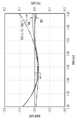
方向性結合器の結合率に偏波依存性が存在するためである。TE偏波とTM偏波の差分であるPDT(Polarization Dependent Transmittance)は、この波長帯域にわたっておよそ0.1dBの偏波依存性が存在する。
図4に、第1の実施形態にかかるWINCの構成を示す。図4(a)に全体構成を示し、図4(b)に方向性結合器の拡大図を示す。WINC20は、2つの方向性結合器21,22の間に2本のアーム導波路23,24を有するマッハツェンダ干渉計により構成されている。アーム導波路23(長アーム)とアーム導波路24(短アーム)との間に光路長差ΔLが設けられている。方向性結合器21,22は非対称方向性結合器であり、結合部における2本の導波路幅が異なっている。図4(b)に示すように、長アームを構成するアーム導波路23の側の導波路幅をW1、短アームを構成するアーム導波路24の側の導波路幅をW2としている。
方向性結合器の一本の入力導波路に入射した光信号が、他方の導波路に100%結合する結合部の長さを完全結合長LCとしたとき、
なる関係を有する。


図5に、第2の実施形態にかかるWINCの構成を示す。図5(a)に全体構成を示し、図5(b)に方向性結合器の拡大図を示す。WINC30は、2つの方向性結合器31,32の間に2本のアーム導波路33,34を有するマッハツェンダ干渉計により構成されている。アーム導波路33(長アーム)とアーム導波路34(短アーム)との間に光路長差ΔLが設けられている。さらに、アーム導波路33の一部分が、2本のアームの導波路の幅Wよりも太い導波路幅WBを有している。方向性結合器31,32は、第1の実施形態と同様に、非対称方向性結合器であり、それぞれ長アーム側の導波路幅をW1、短アーム側の導波路幅をW2としている。
Claims (1)
- 2つの方向性結合器の間に2本のアーム導波路を有するマッハツェンダ干渉計により構成された導波路型光カプラにおいて、
前記2つの方向性結合器の結合部における2本の導波路幅が互いに異なり、
前記2本のアーム導波路間に光路長差が設けられており、
前記2本のアーム導波路のうち、光路の長いアーム導波路の一部分の導波路幅が、光路の短いアーム導波路の導波路幅よりも広く、
前記2つの方向性結合器の前記結合部における前記2本の導波路幅のうちの幅の細い導波路が、前記2本のアーム導波路のうちの前記光路の長いアーム導波路と接続されていることを特徴とする導波路型光カプラ。
Applications Claiming Priority (1)
| Application Number | Priority Date | Filing Date | Title |
|---|---|---|---|
| PCT/JP2021/044134 WO2023100297A1 (ja) | 2021-12-01 | 2021-12-01 | 導波路型光カプラ |
Publications (2)
| Publication Number | Publication Date |
|---|---|
| JPWO2023100297A1 JPWO2023100297A1 (ja) | 2023-06-08 |
| JP7680693B2 true JP7680693B2 (ja) | 2025-05-21 |
Family
ID=86611657
Family Applications (1)
| Application Number | Title | Priority Date | Filing Date |
|---|---|---|---|
| JP2023564345A Active JP7680693B2 (ja) | 2021-12-01 | 2021-12-01 | 導波路型光カプラ |
Country Status (3)
| Country | Link |
|---|---|
| US (1) | US20250020865A1 (ja) |
| JP (1) | JP7680693B2 (ja) |
| WO (1) | WO2023100297A1 (ja) |
Citations (5)
| Publication number | Priority date | Publication date | Assignee | Title |
|---|---|---|---|---|
| JP2013068909A (ja) | 2011-09-26 | 2013-04-18 | Oki Electric Ind Co Ltd | 光素子 |
| JP2014170076A (ja) | 2013-03-01 | 2014-09-18 | Oki Electric Ind Co Ltd | 光干渉器 |
| JP2018004692A (ja) | 2016-06-27 | 2018-01-11 | 日本電信電話株式会社 | 導波路型光カプラ |
| JP2018036582A (ja) | 2016-09-02 | 2018-03-08 | 日本電信電話株式会社 | モード合分波器及びモード多重伝送システム |
| US10935726B1 (en) | 2019-10-04 | 2021-03-02 | Cisco Technology, Inc. | Integrated broadband optical couplers with robustness to manufacturing variation |
Family Cites Families (1)
| Publication number | Priority date | Publication date | Assignee | Title |
|---|---|---|---|---|
| JPH06308338A (ja) * | 1993-04-23 | 1994-11-04 | Furukawa Electric Co Ltd:The | 導波路型光部品 |
-
2021
- 2021-12-01 JP JP2023564345A patent/JP7680693B2/ja active Active
- 2021-12-01 US US18/710,066 patent/US20250020865A1/en active Pending
- 2021-12-01 WO PCT/JP2021/044134 patent/WO2023100297A1/ja not_active Ceased
Patent Citations (5)
| Publication number | Priority date | Publication date | Assignee | Title |
|---|---|---|---|---|
| JP2013068909A (ja) | 2011-09-26 | 2013-04-18 | Oki Electric Ind Co Ltd | 光素子 |
| JP2014170076A (ja) | 2013-03-01 | 2014-09-18 | Oki Electric Ind Co Ltd | 光干渉器 |
| JP2018004692A (ja) | 2016-06-27 | 2018-01-11 | 日本電信電話株式会社 | 導波路型光カプラ |
| JP2018036582A (ja) | 2016-09-02 | 2018-03-08 | 日本電信電話株式会社 | モード合分波器及びモード多重伝送システム |
| US10935726B1 (en) | 2019-10-04 | 2021-03-02 | Cisco Technology, Inc. | Integrated broadband optical couplers with robustness to manufacturing variation |
Also Published As
| Publication number | Publication date |
|---|---|
| WO2023100297A1 (ja) | 2023-06-08 |
| JPWO2023100297A1 (ja) | 2023-06-08 |
| US20250020865A1 (en) | 2025-01-16 |
Similar Documents
| Publication | Publication Date | Title |
|---|---|---|
| US8787710B2 (en) | Wideband interferometer type polarization light beam combiner and splitter | |
| US8923660B2 (en) | System and method for an optical phase shifter | |
| US9075251B2 (en) | Integrated photonic devices with reduced sensitivity to external influences | |
| JP4102792B2 (ja) | 導波路型光干渉計 | |
| US9164350B2 (en) | Multi-port optical circulator system | |
| JP5075840B2 (ja) | 導波路型光干渉回路 | |
| US5341444A (en) | Polarization compensated integrated optical filters and multiplexers | |
| JP2005010805A6 (ja) | 導波路型光干渉計 | |
| JPWO2001059495A1 (ja) | 導波路型光干渉計 | |
| US20030039461A1 (en) | Polarization-insensitive variable optical attenuator | |
| US20120163751A1 (en) | Reflection type optical delay interferometer apparatus based on planar waveguide | |
| WO2009104664A1 (ja) | 導波路型光デバイス | |
| JP4158588B2 (ja) | 導波路型光可変減衰器 | |
| JP4449236B2 (ja) | 光デバイス | |
| Deng et al. | Polarization-insensitive and broadband optical power splitter with a tunable power splitting ratio | |
| US6892021B2 (en) | Dynamic gain equalization arrangement for optical signals | |
| JP7680693B2 (ja) | 導波路型光カプラ | |
| Uematsu et al. | Ultra-broadband silicon-wire polarization beam combiner/splitter based on a wavelength insensitive coupler with a point-symmetrical configuration | |
| JP5137619B2 (ja) | Plc型可変分散補償器 | |
| JP2001272561A (ja) | 偏波無依存導波路型光回路 | |
| US6819859B2 (en) | Planar lightwave circuit type variable optical attenuator | |
| JP7846419B2 (ja) | 利得等化器 | |
| CN104991309A (zh) | 一种补偿阵列波导光栅偏振敏感性的方法 | |
| US12451966B1 (en) | Optical communication systems and silicon photonics passive multiplexers and demultiplexers having Mach-Zehnder interferometer structures | |
| Iguchi et al. | New insights of polarization beam splitter based on sinusoidally driven directional coupler |
Legal Events
| Date | Code | Title | Description |
|---|---|---|---|
| A621 | Written request for application examination |
Free format text: JAPANESE INTERMEDIATE CODE: A621 Effective date: 20240507 |
|
| A131 | Notification of reasons for refusal |
Free format text: JAPANESE INTERMEDIATE CODE: A131 Effective date: 20241224 |
|
| A521 | Request for written amendment filed |
Free format text: JAPANESE INTERMEDIATE CODE: A523 Effective date: 20250218 |
|
| TRDD | Decision of grant or rejection written | ||
| A01 | Written decision to grant a patent or to grant a registration (utility model) |
Free format text: JAPANESE INTERMEDIATE CODE: A01 Effective date: 20250408 |
|
| A61 | First payment of annual fees (during grant procedure) |
Free format text: JAPANESE INTERMEDIATE CODE: A61 Effective date: 20250421 |
|
| R150 | Certificate of patent or registration of utility model |
Ref document number: 7680693 Country of ref document: JP Free format text: JAPANESE INTERMEDIATE CODE: R150 |
|
| S533 | Written request for registration of change of name |
Free format text: JAPANESE INTERMEDIATE CODE: R313533 |
|
| R350 | Written notification of registration of transfer |
Free format text: JAPANESE INTERMEDIATE CODE: R350 |