JP7621635B2 - 三次元発光ダイオードを備えた光電子デバイス - Google Patents
三次元発光ダイオードを備えた光電子デバイス Download PDFInfo
- Publication number
- JP7621635B2 JP7621635B2 JP2020536272A JP2020536272A JP7621635B2 JP 7621635 B2 JP7621635 B2 JP 7621635B2 JP 2020536272 A JP2020536272 A JP 2020536272A JP 2020536272 A JP2020536272 A JP 2020536272A JP 7621635 B2 JP7621635 B2 JP 7621635B2
- Authority
- JP
- Japan
- Prior art keywords
- layer
- chemical element
- substrate
- optoelectronic device
- formed primarily
- Prior art date
- Legal status (The legal status is an assumption and is not a legal conclusion. Google has not performed a legal analysis and makes no representation as to the accuracy of the status listed.)
- Active
Links
Images

Classifications
-
- H—ELECTRICITY
- H10—SEMICONDUCTOR DEVICES; ELECTRIC SOLID-STATE DEVICES NOT OTHERWISE PROVIDED FOR
- H10H—INORGANIC LIGHT-EMITTING SEMICONDUCTOR DEVICES HAVING POTENTIAL BARRIERS
- H10H20/00—Individual inorganic light-emitting semiconductor devices having potential barriers, e.g. light-emitting diodes [LED]
- H10H20/80—Constructional details
- H10H20/81—Bodies
- H10H20/816—Bodies having carrier transport control structures, e.g. highly-doped semiconductor layers or current-blocking structures
- H10H20/8162—Current-blocking structures
-
- H—ELECTRICITY
- H10—SEMICONDUCTOR DEVICES; ELECTRIC SOLID-STATE DEVICES NOT OTHERWISE PROVIDED FOR
- H10H—INORGANIC LIGHT-EMITTING SEMICONDUCTOR DEVICES HAVING POTENTIAL BARRIERS
- H10H20/00—Individual inorganic light-emitting semiconductor devices having potential barriers, e.g. light-emitting diodes [LED]
- H10H20/80—Constructional details
- H10H20/81—Bodies
- H10H20/811—Bodies having quantum effect structures or superlattices, e.g. tunnel junctions
- H10H20/812—Bodies having quantum effect structures or superlattices, e.g. tunnel junctions within the light-emitting regions, e.g. having quantum confinement structures
-
- H—ELECTRICITY
- H10—SEMICONDUCTOR DEVICES; ELECTRIC SOLID-STATE DEVICES NOT OTHERWISE PROVIDED FOR
- H10H—INORGANIC LIGHT-EMITTING SEMICONDUCTOR DEVICES HAVING POTENTIAL BARRIERS
- H10H20/00—Individual inorganic light-emitting semiconductor devices having potential barriers, e.g. light-emitting diodes [LED]
- H10H20/80—Constructional details
- H10H20/81—Bodies
- H10H20/819—Bodies characterised by their shape, e.g. curved or truncated substrates
- H10H20/821—Bodies characterised by their shape, e.g. curved or truncated substrates of the light-emitting regions, e.g. non-planar junctions
-
- H—ELECTRICITY
- H10—SEMICONDUCTOR DEVICES; ELECTRIC SOLID-STATE DEVICES NOT OTHERWISE PROVIDED FOR
- H10H—INORGANIC LIGHT-EMITTING SEMICONDUCTOR DEVICES HAVING POTENTIAL BARRIERS
- H10H20/00—Individual inorganic light-emitting semiconductor devices having potential barriers, e.g. light-emitting diodes [LED]
- H10H20/80—Constructional details
- H10H20/81—Bodies
- H10H20/822—Materials of the light-emitting regions
- H10H20/824—Materials of the light-emitting regions comprising only Group III-V materials, e.g. GaP
-
- H—ELECTRICITY
- H10—SEMICONDUCTOR DEVICES; ELECTRIC SOLID-STATE DEVICES NOT OTHERWISE PROVIDED FOR
- H10H—INORGANIC LIGHT-EMITTING SEMICONDUCTOR DEVICES HAVING POTENTIAL BARRIERS
- H10H20/00—Individual inorganic light-emitting semiconductor devices having potential barriers, e.g. light-emitting diodes [LED]
- H10H20/80—Constructional details
- H10H20/83—Electrodes
-
- H—ELECTRICITY
- H10—SEMICONDUCTOR DEVICES; ELECTRIC SOLID-STATE DEVICES NOT OTHERWISE PROVIDED FOR
- H10H—INORGANIC LIGHT-EMITTING SEMICONDUCTOR DEVICES HAVING POTENTIAL BARRIERS
- H10H20/00—Individual inorganic light-emitting semiconductor devices having potential barriers, e.g. light-emitting diodes [LED]
- H10H20/80—Constructional details
- H10H20/81—Bodies
- H10H20/817—Bodies characterised by the crystal structures or orientations, e.g. polycrystalline, amorphous or porous
-
- H—ELECTRICITY
- H10—SEMICONDUCTOR DEVICES; ELECTRIC SOLID-STATE DEVICES NOT OTHERWISE PROVIDED FOR
- H10H—INORGANIC LIGHT-EMITTING SEMICONDUCTOR DEVICES HAVING POTENTIAL BARRIERS
- H10H20/00—Individual inorganic light-emitting semiconductor devices having potential barriers, e.g. light-emitting diodes [LED]
- H10H20/80—Constructional details
- H10H20/81—Bodies
- H10H20/822—Materials of the light-emitting regions
- H10H20/824—Materials of the light-emitting regions comprising only Group III-V materials, e.g. GaP
- H10H20/825—Materials of the light-emitting regions comprising only Group III-V materials, e.g. GaP containing nitrogen, e.g. GaN
Landscapes
- Led Devices (AREA)
- Led Device Packages (AREA)
Description
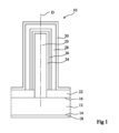
基板と、
主に第1の化学元素及び第2の化学元素で形成され、前記基板に置かれている三次元半導体素子と、
前記三次元半導体素子の側壁を少なくとも部分的に覆って、主に前記第1の化学元素及び前記第2の化学元素で形成された少なくとも第1の層、並びに主に前記第1の化学元素、前記第2の化学元素及び第3の化学元素で形成された少なくとも第2の層の積層体を有するアクティブ領域と、
前記アクティブ領域を覆って、主に前記第1の化学元素、前記第2の化学元素、前記第3の化学元素及び第4の化学元素で形成された第3の層と
を備えており、
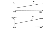
前記第3の層の前記第3の化学元素及び前記第4の化学元素の質量比率が、前記基板との距離が増加するにつれて増加又は減少し、
前記光電子デバイスは、前記第3の層を覆って、主に前記第1の化学元素及び前記第2の化学元素で形成された第4の層を更に備えていることを特徴とする光電子デバイスを提供する。
Claims (4)
- 光電子デバイスであって、
基板と、
主にガリウム及び窒素で形成され、前記基板に置かれているワイヤ状又は角錐状の三次元半導体素子と、
前記三次元半導体素子の側壁を少なくとも部分的に覆って電磁放射線を放射することができ、主にガリウム及び窒素で形成された少なくとも第1の層、並びに主にガリウム、窒素及びインジウムで形成された少なくとも第2の層の積層体を有するアクティブ領域と、
前記アクティブ領域を覆って、主にガリウム、窒素、インジウム及びアルミニウムで形成された電子遮断層と
を備えており、
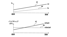
前記電子遮断層のインジウム及びアルミニウムの両方の質量比率が、前記基板との距離が増加するにつれていずれも増加又はいずれも減少し、
前記光電子デバイスは、前記電子遮断層を覆って、主にガリウム及び窒素で形成された層を更に備えていることを特徴とする光電子デバイス。 - 前記電子遮断層のインジウムの含有量が0.1 ~10%の範囲内であることを特徴とする請求項1に記載の光電子デバイス。
- 前記電子遮断層のアルミニウムの含有量が10~40%の範囲内であることを特徴とする請求項1又は2に記載の光電子デバイス。
- 前記電子遮断層のバンドギャップの最大変化が、インジウムを含まない場合のバンドギャップの最大変化より小さいことを特徴とする請求項1~3のいずれか1つに記載の光電子デバイス。
Applications Claiming Priority (3)
| Application Number | Priority Date | Filing Date | Title |
|---|---|---|---|
| FR1763316A FR3076399B1 (fr) | 2017-12-28 | 2017-12-28 | Dispositif optoelectronique comprenant des diodes electroluminescentes tridimensionnelles |
| FR1763316 | 2017-12-28 | ||
| PCT/EP2018/083890 WO2019129473A1 (fr) | 2017-12-28 | 2018-12-06 | Dispositif optoelectronique comprenant des diodes electroluminescentes tridimensionnelles |
Publications (2)
| Publication Number | Publication Date |
|---|---|
| JP2021508951A JP2021508951A (ja) | 2021-03-11 |
| JP7621635B2 true JP7621635B2 (ja) | 2025-01-27 |
Family
ID=62017441
Family Applications (1)
| Application Number | Title | Priority Date | Filing Date |
|---|---|---|---|
| JP2020536272A Active JP7621635B2 (ja) | 2017-12-28 | 2018-12-06 | 三次元発光ダイオードを備えた光電子デバイス |
Country Status (8)
| Country | Link |
|---|---|
| US (1) | US11563147B2 (ja) |
| EP (1) | EP3732735A1 (ja) |
| JP (1) | JP7621635B2 (ja) |
| KR (1) | KR102572289B1 (ja) |
| CN (1) | CN111788701B (ja) |
| FR (1) | FR3076399B1 (ja) |
| TW (1) | TWI805657B (ja) |
| WO (1) | WO2019129473A1 (ja) |
Cited By (1)
| Publication number | Priority date | Publication date | Assignee | Title |
|---|---|---|---|---|
| US9663427B2 (en) | 2003-11-20 | 2017-05-30 | Solvay (Société Anonyme) | Process for producing epichlorohydrin |
Families Citing this family (2)
| Publication number | Priority date | Publication date | Assignee | Title |
|---|---|---|---|---|
| FR3096509B1 (fr) * | 2019-05-20 | 2021-05-28 | Aledia | Dispositif optoelectronique avec diodes electroluminescentes dont une zone dopee integre une portion externe a base d’aluminium et de nitrure de galium |
| FR3124024A1 (fr) * | 2021-06-11 | 2022-12-16 | Aledia | Procédé de fabrication d’un dispositif optoélectronique |
Citations (4)
| Publication number | Priority date | Publication date | Assignee | Title |
|---|---|---|---|---|
| JP2015511776A (ja) | 2012-03-29 | 2015-04-20 | ソウル バイオシス カンパニー リミテッドSeoul Viosys Co.,Ltd. | 発光素子 |
| JP2016521459A (ja) | 2013-04-26 | 2016-07-21 | オスラム オプト セミコンダクターズ ゲゼルシャフト ミット ベシュレンクテル ハフツングOsram Opto Semiconductors GmbH | 活性ゾーンを有する半導体積層体を円柱状構造上に備えた発光アセンブリ |
| WO2016208993A1 (ko) | 2015-06-23 | 2016-12-29 | 엘지이노텍 주식회사 | 발광소자 및 이를 포함하는 표시장치 |
| JP2017503333A (ja) | 2013-12-17 | 2017-01-26 | グロ アーベーGlo Ab | 歪み修正面活性領域を有するiii族窒化物ナノワイヤled及びその製造方法 |
Family Cites Families (12)
| Publication number | Priority date | Publication date | Assignee | Title |
|---|---|---|---|---|
| JP4572963B2 (ja) * | 2008-07-09 | 2010-11-04 | 住友電気工業株式会社 | Iii族窒化物系半導体発光素子、及びエピタキシャルウエハ |
| KR101650720B1 (ko) * | 2010-08-04 | 2016-09-06 | 삼성전자주식회사 | 나노로드 기반의 반도체 발광 소자 및 그 제조 방법 |
| US8350249B1 (en) * | 2011-09-26 | 2013-01-08 | Glo Ab | Coalesced nanowire structures with interstitial voids and method for manufacturing the same |
| KR20130108935A (ko) * | 2012-03-26 | 2013-10-07 | 서울바이오시스 주식회사 | 질화갈륨계 발광 다이오드 |
| KR101976455B1 (ko) * | 2012-10-19 | 2019-05-09 | 엘지이노텍 주식회사 | 발광 소자 및 발광 소자 패키지 |
| US20140264260A1 (en) * | 2013-03-15 | 2014-09-18 | Design Express Limited | Light emitting structure |
| US9196787B2 (en) * | 2013-06-07 | 2015-11-24 | Glo Ab | Nanowire LED structure with decreased leakage and method of making same |
| FR3026564B1 (fr) * | 2014-09-30 | 2018-02-16 | Commissariat A L'energie Atomique Et Aux Energies Alternatives | Dispositif optoelectronique a elements semiconducteurs tridimensionnels |
| FR3029015B1 (fr) * | 2014-11-24 | 2018-03-02 | Commissariat A L'energie Atomique Et Aux Energies Alternatives | Dispositif optoelectronique a elements semiconducteurs tridimensionnels et son procede de fabrication |
| FR3032064B1 (fr) * | 2015-01-22 | 2018-03-09 | Aledia | Dispositif optoelectronique et son procede de fabrication |
| KR102523696B1 (ko) * | 2015-11-30 | 2023-04-20 | 쑤저우 레킨 세미컨덕터 컴퍼니 리미티드 | 발광소자 및 그 제조방법 |
| FR3041476B1 (fr) * | 2015-09-21 | 2017-12-01 | Commissariat Energie Atomique | Dispositif electroluminescent a puits quantiques multiples |
-
2017
- 2017-12-28 FR FR1763316A patent/FR3076399B1/fr active Active
-
2018
- 2018-12-06 KR KR1020207020756A patent/KR102572289B1/ko active Active
- 2018-12-06 US US16/958,130 patent/US11563147B2/en active Active
- 2018-12-06 WO PCT/EP2018/083890 patent/WO2019129473A1/fr not_active Ceased
- 2018-12-06 JP JP2020536272A patent/JP7621635B2/ja active Active
- 2018-12-06 CN CN201880090490.5A patent/CN111788701B/zh active Active
- 2018-12-06 EP EP18811318.7A patent/EP3732735A1/fr active Pending
- 2018-12-07 TW TW107144095A patent/TWI805657B/zh active
Patent Citations (4)
| Publication number | Priority date | Publication date | Assignee | Title |
|---|---|---|---|---|
| JP2015511776A (ja) | 2012-03-29 | 2015-04-20 | ソウル バイオシス カンパニー リミテッドSeoul Viosys Co.,Ltd. | 発光素子 |
| JP2016521459A (ja) | 2013-04-26 | 2016-07-21 | オスラム オプト セミコンダクターズ ゲゼルシャフト ミット ベシュレンクテル ハフツングOsram Opto Semiconductors GmbH | 活性ゾーンを有する半導体積層体を円柱状構造上に備えた発光アセンブリ |
| JP2017503333A (ja) | 2013-12-17 | 2017-01-26 | グロ アーベーGlo Ab | 歪み修正面活性領域を有するiii族窒化物ナノワイヤled及びその製造方法 |
| WO2016208993A1 (ko) | 2015-06-23 | 2016-12-29 | 엘지이노텍 주식회사 | 발광소자 및 이를 포함하는 표시장치 |
Cited By (1)
| Publication number | Priority date | Publication date | Assignee | Title |
|---|---|---|---|---|
| US9663427B2 (en) | 2003-11-20 | 2017-05-30 | Solvay (Société Anonyme) | Process for producing epichlorohydrin |
Also Published As
| Publication number | Publication date |
|---|---|
| WO2019129473A1 (fr) | 2019-07-04 |
| EP3732735A1 (fr) | 2020-11-04 |
| FR3076399A1 (fr) | 2019-07-05 |
| KR20200094790A (ko) | 2020-08-07 |
| KR102572289B1 (ko) | 2023-08-28 |
| TW201931622A (zh) | 2019-08-01 |
| JP2021508951A (ja) | 2021-03-11 |
| US20200365762A1 (en) | 2020-11-19 |
| US11563147B2 (en) | 2023-01-24 |
| CN111788701A (zh) | 2020-10-16 |
| CN111788701B (zh) | 2024-12-20 |
| FR3076399B1 (fr) | 2020-01-24 |
| TWI805657B (zh) | 2023-06-21 |
Similar Documents
| Publication | Publication Date | Title |
|---|---|---|
| TWI775886B (zh) | 包括以軸向配置的三維半導體結構之光電裝置 | |
| US8835902B2 (en) | Nano-structured light-emitting devices | |
| US8455284B2 (en) | Group III nitride nanorod light emitting device and method of manufacturing thereof | |
| US10651341B2 (en) | Optoelectronic device and method for manufacturing same | |
| US8890184B2 (en) | Nanostructured light-emitting device | |
| KR20220140749A (ko) | 적색 led 및 제작 방법 | |
| CN111066161B (zh) | 氮化物半导体发光元件和氮化物半导体发光元件的制造方法 | |
| US20150171263A1 (en) | Nitride semiconductor light emitting element and method for manufacturing same | |
| KR102389679B1 (ko) | 3차원 반도체 소자를 구비한 광전자 장치 | |
| US10801129B2 (en) | Nucleation structure suitable for epitaxial growth of three-dimensional semiconductor elements | |
| KR102572289B1 (ko) | 3차원 발광 다이오드를 갖는 광전자 장치 | |
| TWI851832B (zh) | 氮化物半導體紫外線發光元件及其製造方法 | |
| US9142717B2 (en) | Semiconductor light emitting device and wafer | |
| US20100127239A1 (en) | III-Nitride Semiconductor Light Emitting Device | |
| US20120292648A1 (en) | Nitride semiconductor device, nitride semiconductor wafer, and method for manufacturing nitride semiconductor layer | |
| US10559713B2 (en) | Multiple quantum well light-emitting device | |
| JP7568300B2 (ja) | マイクロワイヤ又はナノワイヤの製造方法 | |
| US8026525B2 (en) | Boron phosphide-based semiconductor light-emitting device | |
| JP7405902B2 (ja) | 窒化物半導体発光素子 | |
| KR20160057664A (ko) | 고효율 발광 소자 |
Legal Events
| Date | Code | Title | Description |
|---|---|---|---|
| A621 | Written request for application examination |
Free format text: JAPANESE INTERMEDIATE CODE: A621 Effective date: 20211006 |
|
| A977 | Report on retrieval |
Free format text: JAPANESE INTERMEDIATE CODE: A971007 Effective date: 20220818 |
|
| A131 | Notification of reasons for refusal |
Free format text: JAPANESE INTERMEDIATE CODE: A131 Effective date: 20220913 |
|
| A521 | Request for written amendment filed |
Free format text: JAPANESE INTERMEDIATE CODE: A523 Effective date: 20221213 |
|
| A02 | Decision of refusal |
Free format text: JAPANESE INTERMEDIATE CODE: A02 Effective date: 20230228 |
|
| A521 | Request for written amendment filed |
Free format text: JAPANESE INTERMEDIATE CODE: A523 Effective date: 20230629 |
|
| A521 | Request for written amendment filed |
Free format text: JAPANESE INTERMEDIATE CODE: A821 Effective date: 20230629 |
|
| A911 | Transfer to examiner for re-examination before appeal (zenchi) |
Free format text: JAPANESE INTERMEDIATE CODE: A911 Effective date: 20230719 |
|
| A912 | Re-examination (zenchi) completed and case transferred to appeal board |
Free format text: JAPANESE INTERMEDIATE CODE: A912 Effective date: 20230915 |
|
| A521 | Request for written amendment filed |
Free format text: JAPANESE INTERMEDIATE CODE: A821 Effective date: 20231211 |
|
| A521 | Request for written amendment filed |
Free format text: JAPANESE INTERMEDIATE CODE: A523 Effective date: 20240917 |
|
| A61 | First payment of annual fees (during grant procedure) |
Free format text: JAPANESE INTERMEDIATE CODE: A61 Effective date: 20250107 |
|
| R150 | Certificate of patent or registration of utility model |
Ref document number: 7621635 Country of ref document: JP Free format text: JAPANESE INTERMEDIATE CODE: R150 |