JP7617954B2 - 半導体装置とその製造方法、および半導体パッケージ - Google Patents
半導体装置とその製造方法、および半導体パッケージ Download PDFInfo
- Publication number
- JP7617954B2 JP7617954B2 JP2022575005A JP2022575005A JP7617954B2 JP 7617954 B2 JP7617954 B2 JP 7617954B2 JP 2022575005 A JP2022575005 A JP 2022575005A JP 2022575005 A JP2022575005 A JP 2022575005A JP 7617954 B2 JP7617954 B2 JP 7617954B2
- Authority
- JP
- Japan
- Prior art keywords
- protrusion
- control board
- flexible wiring
- semiconductor package
- semiconductor
- Prior art date
- Legal status (The legal status is an assumption and is not a legal conclusion. Google has not performed a legal analysis and makes no representation as to the accuracy of the status listed.)
- Active
Links
Images


Classifications
-
- H—ELECTRICITY
- H01—ELECTRIC ELEMENTS
- H01L—SEMICONDUCTOR DEVICES NOT COVERED BY CLASS H10
- H01L25/00—Assemblies consisting of a plurality of semiconductor or other solid state devices
- H01L25/16—Assemblies consisting of a plurality of semiconductor or other solid state devices the devices being of types provided for in two or more different subclasses of H10B, H10D, H10F, H10H, H10K or H10N, e.g. forming hybrid circuits
- H01L25/165—Containers
-
- H—ELECTRICITY
- H01—ELECTRIC ELEMENTS
- H01L—SEMICONDUCTOR DEVICES NOT COVERED BY CLASS H10
- H01L23/00—Details of semiconductor or other solid state devices
- H01L23/562—Protection against mechanical damage
-
- H—ELECTRICITY
- H01—ELECTRIC ELEMENTS
- H01L—SEMICONDUCTOR DEVICES NOT COVERED BY CLASS H10
- H01L23/00—Details of semiconductor or other solid state devices
- H01L23/28—Encapsulations, e.g. encapsulating layers, coatings, e.g. for protection
- H01L23/29—Encapsulations, e.g. encapsulating layers, coatings, e.g. for protection characterised by the material, e.g. carbon
- H01L23/293—Organic, e.g. plastic
-
- H—ELECTRICITY
- H01—ELECTRIC ELEMENTS
- H01L—SEMICONDUCTOR DEVICES NOT COVERED BY CLASS H10
- H01L23/00—Details of semiconductor or other solid state devices
- H01L23/28—Encapsulations, e.g. encapsulating layers, coatings, e.g. for protection
- H01L23/31—Encapsulations, e.g. encapsulating layers, coatings, e.g. for protection characterised by the arrangement or shape
- H01L23/3107—Encapsulations, e.g. encapsulating layers, coatings, e.g. for protection characterised by the arrangement or shape the device being completely enclosed
- H01L23/3121—Encapsulations, e.g. encapsulating layers, coatings, e.g. for protection characterised by the arrangement or shape the device being completely enclosed a substrate forming part of the encapsulation
-
- H—ELECTRICITY
- H01—ELECTRIC ELEMENTS
- H01L—SEMICONDUCTOR DEVICES NOT COVERED BY CLASS H10
- H01L23/00—Details of semiconductor or other solid state devices
- H01L23/28—Encapsulations, e.g. encapsulating layers, coatings, e.g. for protection
- H01L23/31—Encapsulations, e.g. encapsulating layers, coatings, e.g. for protection characterised by the arrangement or shape
- H01L23/3107—Encapsulations, e.g. encapsulating layers, coatings, e.g. for protection characterised by the arrangement or shape the device being completely enclosed
- H01L23/3142—Sealing arrangements between parts, e.g. adhesion promotors
-
- H—ELECTRICITY
- H01—ELECTRIC ELEMENTS
- H01L—SEMICONDUCTOR DEVICES NOT COVERED BY CLASS H10
- H01L23/00—Details of semiconductor or other solid state devices
- H01L23/48—Arrangements for conducting electric current to or from the solid state body in operation, e.g. leads, terminal arrangements ; Selection of materials therefor
- H01L23/488—Arrangements for conducting electric current to or from the solid state body in operation, e.g. leads, terminal arrangements ; Selection of materials therefor consisting of soldered or bonded constructions
- H01L23/498—Leads, i.e. metallisations or lead-frames on insulating substrates, e.g. chip carriers
- H01L23/49811—Additional leads joined to the metallisation on the insulating substrate, e.g. pins, bumps, wires, flat leads
-
- H—ELECTRICITY
- H01—ELECTRIC ELEMENTS
- H01L—SEMICONDUCTOR DEVICES NOT COVERED BY CLASS H10
- H01L24/00—Arrangements for connecting or disconnecting semiconductor or solid-state bodies; Methods or apparatus related thereto
- H01L24/01—Means for bonding being attached to, or being formed on, the surface to be connected, e.g. chip-to-package, die-attach, "first-level" interconnects; Manufacturing methods related thereto
- H01L24/10—Bump connectors ; Manufacturing methods related thereto
- H01L24/15—Structure, shape, material or disposition of the bump connectors after the connecting process
- H01L24/16—Structure, shape, material or disposition of the bump connectors after the connecting process of an individual bump connector
-
- H—ELECTRICITY
- H01—ELECTRIC ELEMENTS
- H01L—SEMICONDUCTOR DEVICES NOT COVERED BY CLASS H10
- H01L24/00—Arrangements for connecting or disconnecting semiconductor or solid-state bodies; Methods or apparatus related thereto
- H01L24/01—Means for bonding being attached to, or being formed on, the surface to be connected, e.g. chip-to-package, die-attach, "first-level" interconnects; Manufacturing methods related thereto
- H01L24/26—Layer connectors, e.g. plate connectors, solder or adhesive layers; Manufacturing methods related thereto
- H01L24/31—Structure, shape, material or disposition of the layer connectors after the connecting process
- H01L24/32—Structure, shape, material or disposition of the layer connectors after the connecting process of an individual layer connector
-
- H—ELECTRICITY
- H01—ELECTRIC ELEMENTS
- H01L—SEMICONDUCTOR DEVICES NOT COVERED BY CLASS H10
- H01L24/00—Arrangements for connecting or disconnecting semiconductor or solid-state bodies; Methods or apparatus related thereto
- H01L24/01—Means for bonding being attached to, or being formed on, the surface to be connected, e.g. chip-to-package, die-attach, "first-level" interconnects; Manufacturing methods related thereto
- H01L24/42—Wire connectors; Manufacturing methods related thereto
- H01L24/47—Structure, shape, material or disposition of the wire connectors after the connecting process
- H01L24/48—Structure, shape, material or disposition of the wire connectors after the connecting process of an individual wire connector
-
- H—ELECTRICITY
- H01—ELECTRIC ELEMENTS
- H01L—SEMICONDUCTOR DEVICES NOT COVERED BY CLASS H10
- H01L24/00—Arrangements for connecting or disconnecting semiconductor or solid-state bodies; Methods or apparatus related thereto
- H01L24/73—Means for bonding being of different types provided for in two or more of groups H01L24/10, H01L24/18, H01L24/26, H01L24/34, H01L24/42, H01L24/50, H01L24/63, H01L24/71
-
- H—ELECTRICITY
- H01—ELECTRIC ELEMENTS
- H01L—SEMICONDUCTOR DEVICES NOT COVERED BY CLASS H10
- H01L25/00—Assemblies consisting of a plurality of semiconductor or other solid state devices
- H01L25/03—Assemblies consisting of a plurality of semiconductor or other solid state devices all the devices being of a type provided for in a single subclass of subclasses H10B, H10D, H10F, H10H, H10K or H10N, e.g. assemblies of rectifier diodes
- H01L25/04—Assemblies consisting of a plurality of semiconductor or other solid state devices all the devices being of a type provided for in a single subclass of subclasses H10B, H10D, H10F, H10H, H10K or H10N, e.g. assemblies of rectifier diodes the devices not having separate containers
- H01L25/07—Assemblies consisting of a plurality of semiconductor or other solid state devices all the devices being of a type provided for in a single subclass of subclasses H10B, H10D, H10F, H10H, H10K or H10N, e.g. assemblies of rectifier diodes the devices not having separate containers the devices being of a type provided for in group subclass H10D
- H01L25/072—Assemblies consisting of a plurality of semiconductor or other solid state devices all the devices being of a type provided for in a single subclass of subclasses H10B, H10D, H10F, H10H, H10K or H10N, e.g. assemblies of rectifier diodes the devices not having separate containers the devices being of a type provided for in group subclass H10D the devices being arranged next to each other
-
- H—ELECTRICITY
- H01—ELECTRIC ELEMENTS
- H01L—SEMICONDUCTOR DEVICES NOT COVERED BY CLASS H10
- H01L25/00—Assemblies consisting of a plurality of semiconductor or other solid state devices
- H01L25/03—Assemblies consisting of a plurality of semiconductor or other solid state devices all the devices being of a type provided for in a single subclass of subclasses H10B, H10D, H10F, H10H, H10K or H10N, e.g. assemblies of rectifier diodes
- H01L25/10—Assemblies consisting of a plurality of semiconductor or other solid state devices all the devices being of a type provided for in a single subclass of subclasses H10B, H10D, H10F, H10H, H10K or H10N, e.g. assemblies of rectifier diodes the devices having separate containers
- H01L25/11—Assemblies consisting of a plurality of semiconductor or other solid state devices all the devices being of a type provided for in a single subclass of subclasses H10B, H10D, H10F, H10H, H10K or H10N, e.g. assemblies of rectifier diodes the devices having separate containers the devices being of a type provided for in subclass H10D
- H01L25/115—Assemblies consisting of a plurality of semiconductor or other solid state devices all the devices being of a type provided for in a single subclass of subclasses H10B, H10D, H10F, H10H, H10K or H10N, e.g. assemblies of rectifier diodes the devices having separate containers the devices being of a type provided for in subclass H10D the devices being arranged next to each other
-
- H—ELECTRICITY
- H01—ELECTRIC ELEMENTS
- H01L—SEMICONDUCTOR DEVICES NOT COVERED BY CLASS H10
- H01L25/00—Assemblies consisting of a plurality of semiconductor or other solid state devices
- H01L25/18—Assemblies consisting of a plurality of semiconductor or other solid state devices the devices being of the types provided for in two or more different main groups of the same subclass of H10B, H10D, H10F, H10H, H10K or H10N
-
- H—ELECTRICITY
- H01—ELECTRIC ELEMENTS
- H01L—SEMICONDUCTOR DEVICES NOT COVERED BY CLASS H10
- H01L2224/00—Indexing scheme for arrangements for connecting or disconnecting semiconductor or solid-state bodies and methods related thereto as covered by H01L24/00
- H01L2224/01—Means for bonding being attached to, or being formed on, the surface to be connected, e.g. chip-to-package, die-attach, "first-level" interconnects; Manufacturing methods related thereto
- H01L2224/26—Layer connectors, e.g. plate connectors, solder or adhesive layers; Manufacturing methods related thereto
- H01L2224/31—Structure, shape, material or disposition of the layer connectors after the connecting process
- H01L2224/32—Structure, shape, material or disposition of the layer connectors after the connecting process of an individual layer connector
- H01L2224/321—Disposition
- H01L2224/32151—Disposition the layer connector connecting between a semiconductor or solid-state body and an item not being a semiconductor or solid-state body, e.g. chip-to-substrate, chip-to-passive
- H01L2224/32221—Disposition the layer connector connecting between a semiconductor or solid-state body and an item not being a semiconductor or solid-state body, e.g. chip-to-substrate, chip-to-passive the body and the item being stacked
- H01L2224/32245—Disposition the layer connector connecting between a semiconductor or solid-state body and an item not being a semiconductor or solid-state body, e.g. chip-to-substrate, chip-to-passive the body and the item being stacked the item being metallic
-
- H—ELECTRICITY
- H01—ELECTRIC ELEMENTS
- H01L—SEMICONDUCTOR DEVICES NOT COVERED BY CLASS H10
- H01L2224/00—Indexing scheme for arrangements for connecting or disconnecting semiconductor or solid-state bodies and methods related thereto as covered by H01L24/00
- H01L2224/01—Means for bonding being attached to, or being formed on, the surface to be connected, e.g. chip-to-package, die-attach, "first-level" interconnects; Manufacturing methods related thereto
- H01L2224/34—Strap connectors, e.g. copper straps for grounding power devices; Manufacturing methods related thereto
- H01L2224/39—Structure, shape, material or disposition of the strap connectors after the connecting process
- H01L2224/40—Structure, shape, material or disposition of the strap connectors after the connecting process of an individual strap connector
- H01L2224/401—Disposition
- H01L2224/40135—Connecting between different semiconductor or solid-state bodies, i.e. chip-to-chip
- H01L2224/40137—Connecting between different semiconductor or solid-state bodies, i.e. chip-to-chip the bodies being arranged next to each other, e.g. on a common substrate
-
- H—ELECTRICITY
- H01—ELECTRIC ELEMENTS
- H01L—SEMICONDUCTOR DEVICES NOT COVERED BY CLASS H10
- H01L2224/00—Indexing scheme for arrangements for connecting or disconnecting semiconductor or solid-state bodies and methods related thereto as covered by H01L24/00
- H01L2224/01—Means for bonding being attached to, or being formed on, the surface to be connected, e.g. chip-to-package, die-attach, "first-level" interconnects; Manufacturing methods related thereto
- H01L2224/42—Wire connectors; Manufacturing methods related thereto
- H01L2224/47—Structure, shape, material or disposition of the wire connectors after the connecting process
- H01L2224/48—Structure, shape, material or disposition of the wire connectors after the connecting process of an individual wire connector
- H01L2224/4805—Shape
- H01L2224/4809—Loop shape
- H01L2224/48091—Arched
-
- H—ELECTRICITY
- H01—ELECTRIC ELEMENTS
- H01L—SEMICONDUCTOR DEVICES NOT COVERED BY CLASS H10
- H01L2224/00—Indexing scheme for arrangements for connecting or disconnecting semiconductor or solid-state bodies and methods related thereto as covered by H01L24/00
- H01L2224/01—Means for bonding being attached to, or being formed on, the surface to be connected, e.g. chip-to-package, die-attach, "first-level" interconnects; Manufacturing methods related thereto
- H01L2224/42—Wire connectors; Manufacturing methods related thereto
- H01L2224/47—Structure, shape, material or disposition of the wire connectors after the connecting process
- H01L2224/48—Structure, shape, material or disposition of the wire connectors after the connecting process of an individual wire connector
- H01L2224/481—Disposition
- H01L2224/48151—Connecting between a semiconductor or solid-state body and an item not being a semiconductor or solid-state body, e.g. chip-to-substrate, chip-to-passive
- H01L2224/48221—Connecting between a semiconductor or solid-state body and an item not being a semiconductor or solid-state body, e.g. chip-to-substrate, chip-to-passive the body and the item being stacked
- H01L2224/48245—Connecting between a semiconductor or solid-state body and an item not being a semiconductor or solid-state body, e.g. chip-to-substrate, chip-to-passive the body and the item being stacked the item being metallic
- H01L2224/48247—Connecting between a semiconductor or solid-state body and an item not being a semiconductor or solid-state body, e.g. chip-to-substrate, chip-to-passive the body and the item being stacked the item being metallic connecting the wire to a bond pad of the item
- H01L2224/48249—Connecting between a semiconductor or solid-state body and an item not being a semiconductor or solid-state body, e.g. chip-to-substrate, chip-to-passive the body and the item being stacked the item being metallic connecting the wire to a bond pad of the item the bond pad protruding from the surface of the item
-
- H—ELECTRICITY
- H01—ELECTRIC ELEMENTS
- H01L—SEMICONDUCTOR DEVICES NOT COVERED BY CLASS H10
- H01L2224/00—Indexing scheme for arrangements for connecting or disconnecting semiconductor or solid-state bodies and methods related thereto as covered by H01L24/00
- H01L2224/01—Means for bonding being attached to, or being formed on, the surface to be connected, e.g. chip-to-package, die-attach, "first-level" interconnects; Manufacturing methods related thereto
- H01L2224/42—Wire connectors; Manufacturing methods related thereto
- H01L2224/47—Structure, shape, material or disposition of the wire connectors after the connecting process
- H01L2224/48—Structure, shape, material or disposition of the wire connectors after the connecting process of an individual wire connector
- H01L2224/484—Connecting portions
- H01L2224/4847—Connecting portions the connecting portion on the bonding area of the semiconductor or solid-state body being a wedge bond
- H01L2224/48472—Connecting portions the connecting portion on the bonding area of the semiconductor or solid-state body being a wedge bond the other connecting portion not on the bonding area also being a wedge bond, i.e. wedge-to-wedge
-
- H—ELECTRICITY
- H01—ELECTRIC ELEMENTS
- H01L—SEMICONDUCTOR DEVICES NOT COVERED BY CLASS H10
- H01L2224/00—Indexing scheme for arrangements for connecting or disconnecting semiconductor or solid-state bodies and methods related thereto as covered by H01L24/00
- H01L2224/73—Means for bonding being of different types provided for in two or more of groups H01L2224/10, H01L2224/18, H01L2224/26, H01L2224/34, H01L2224/42, H01L2224/50, H01L2224/63, H01L2224/71
- H01L2224/732—Location after the connecting process
- H01L2224/73251—Location after the connecting process on different surfaces
- H01L2224/73265—Layer and wire connectors
-
- H—ELECTRICITY
- H01—ELECTRIC ELEMENTS
- H01L—SEMICONDUCTOR DEVICES NOT COVERED BY CLASS H10
- H01L24/00—Arrangements for connecting or disconnecting semiconductor or solid-state bodies; Methods or apparatus related thereto
- H01L24/01—Means for bonding being attached to, or being formed on, the surface to be connected, e.g. chip-to-package, die-attach, "first-level" interconnects; Manufacturing methods related thereto
- H01L24/63—Connectors not provided for in any of the groups H01L24/10 - H01L24/50 and subgroups; Manufacturing methods related thereto
- H01L24/68—Structure, shape, material or disposition of the connectors after the connecting process
- H01L24/69—Structure, shape, material or disposition of the connectors after the connecting process of an individual connector
-
- H—ELECTRICITY
- H01—ELECTRIC ELEMENTS
- H01L—SEMICONDUCTOR DEVICES NOT COVERED BY CLASS H10
- H01L2924/00—Indexing scheme for arrangements or methods for connecting or disconnecting semiconductor or solid-state bodies as covered by H01L24/00
- H01L2924/10—Details of semiconductor or other solid state devices to be connected
- H01L2924/11—Device type
- H01L2924/13—Discrete devices, e.g. 3 terminal devices
- H01L2924/1304—Transistor
- H01L2924/1306—Field-effect transistor [FET]
- H01L2924/13091—Metal-Oxide-Semiconductor Field-Effect Transistor [MOSFET]
-
- H—ELECTRICITY
- H01—ELECTRIC ELEMENTS
- H01L—SEMICONDUCTOR DEVICES NOT COVERED BY CLASS H10
- H01L2924/00—Indexing scheme for arrangements or methods for connecting or disconnecting semiconductor or solid-state bodies as covered by H01L24/00
- H01L2924/15—Details of package parts other than the semiconductor or other solid state devices to be connected
- H01L2924/181—Encapsulation
Landscapes
- Engineering & Computer Science (AREA)
- Microelectronics & Electronic Packaging (AREA)
- Power Engineering (AREA)
- Computer Hardware Design (AREA)
- Physics & Mathematics (AREA)
- Condensed Matter Physics & Semiconductors (AREA)
- General Physics & Mathematics (AREA)
- Structures Or Materials For Encapsulating Or Coating Semiconductor Devices Or Solid State Devices (AREA)
Description
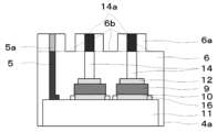
図1は、本実施の形態の半導体装置1の概略構成を示す模式図である。半導体装置1は、ベース板2の上に絶縁部材3を介して半導体パッケージ4が固定され、半導体パッケージ4の導電部材5の先端部5aと制御基板7の制御電極7bとを可撓性配線8で接続した構成である。半導体パッケージ4および制御基板7の詳細については後述するが、ここでは半導体パッケージ4に形成した突出部6aは、制御基板7の貫通孔7aに挿入された状態となっている。
実施の形態1では、半導体パッケージ4の突出部6aの形状は直方体である例を示したが、本実施の形態では、突出部6aは階段状の形状である例について説明する。これ以外の構成は実施の形態1と同様である。
Claims (14)
- 半導体素子と、
前記半導体素子と電気的に接続され、上方に向かって伸びる、複数の導電部材と、
前記半導体素子と前記導電部材とを封止するとともに、前記複数の導電部材の先端部の周囲を覆う突出部を形成する封止樹脂と、
前記突出部が挿入される貫通孔が形成され、制御電極を有する制御基板と、
前記制御電極と前記導電部材の前記先端部とを接続し、可撓性を有する可撓性配線と
を備える半導体装置。 - 前記突出部の下端から前記突出部の上端までの長さである前記突出部の高さは、前記制御基板の厚み以上であり、前記突出部の上端が前記制御基板の上面よりも上方にあることを特徴とする、請求項1に記載の半導体装置。
- 前記突出部は、前記制御基板の下面を支持する支持部を有する下段と、前記貫通孔に挿入する挿入部を有する上段とを備え、前記挿入部の高さは、前記制御基板の厚み以上であり、前記挿入部の上端が前記制御基板の上面よりも上方にあることを特徴とする、請求項1に記載の半導体装置。
- 前記封止樹脂の前記突出部以外の上面は平坦であることを特徴とする、請求項1から請求項3のいずれか一項に記載の半導体装置。
- 前記可撓性配線と前記先端部との接続点である第一接続点および前記可撓性配線と前記制御電極との接続点である第二接続点の間の長さである接続点間距離と、前記第一接続点から前記第二接続点までの前記可撓性配線の長さと、前記突出部の側部と前記貫通孔の開口端との幅である許容幅との関係において、前記可撓性配線の長さは前記接続点間距離と前記許容幅との和よりも長いことを特徴とする、請求項1から請求項4のいずれか一項に記載の半導体装置。
- さらに、前記先端部、前記制御電極および前記可撓性配線を覆い、
これらの間を電気的に絶縁する接合保護部材が前記制御基板上に形成されていることを特徴とする、請求項1から請求項5のいずれか一項に記載の半導体装置。 - 前記封止樹脂の前記突出部以外の上面に、前記導電部材を含まない前記封止樹脂からなる第二突出部が備えられ、前記第二突出部に対応して設けられた前記制御基板の第二貫通孔に前記第二突出部が挿入された構造を有することを特徴とする、請求項1から請求項6のいずれか一項に記載の半導体装置。
- 複数の導電部材の先端部の周囲を覆う突出部を形成する封止樹脂を有した半導体パッケージを、ベース板に固定する半導体パッケージ固定工程と、
前記突出部を制御基板に設けた貫通孔に挿入する突出部挿入工程と、
前記先端部と前記制御基板に設けた制御電極とを、ワイヤボンディングにより可撓性配線で接続する可撓性配線接続工程と
を備える半導体装置の製造方法。 - さらに、前記制御基板の上に、前記先端部、前記制御電極および前記可撓性配線を覆い、これらの間を電気的に絶縁する接合保護部材を形成する接合保護部材形成工程を備えることを特徴とする、請求項8に記載の半導体装置の製造方法。
- 半導体素子と、
前記半導体素子と電気的に接続され、上方に向かって伸びる、複数の導電部材と、
前記半導体素子と前記導電部材とを封止するとともに、前記複数の導電部材の先端部の周囲の一周分を覆う突出部とを形成する封止樹脂と
を備える半導体パッケージ。 - 前記突出部は、支持部を有する下段と、前記下段の上に挿入部を有する上段とで構成され、前記下段の径は前記上段の径よりも大きいことを特徴とする、請求項10に記載の半導体パッケージ。
- 前記封止樹脂の前記突出部以外の上面は平坦であることを特徴とする、請求項10または請求項11に記載の半導体パッケージ。
- さらに、前記封止樹脂の前記突出部以外の上面に、前記導電部材を含まない前記封止樹脂からなる第二突出部が備えられたことを特徴とする、請求項10から請求項12のいずれか一項に記載の半導体パッケージ。
- 前記突出部は、前記複数の導電部材の先端部の上部の周囲を覆わない、請求項10から請求項13のいずれか一項に記載の半導体パッケージ。
Applications Claiming Priority (1)
| Application Number | Priority Date | Filing Date | Title |
|---|---|---|---|
| PCT/JP2021/001341 WO2022153501A1 (ja) | 2021-01-15 | 2021-01-15 | 半導体装置とその製造方法、および半導体パッケージ |
Publications (3)
| Publication Number | Publication Date |
|---|---|
| JPWO2022153501A1 JPWO2022153501A1 (ja) | 2022-07-21 |
| JPWO2022153501A5 JPWO2022153501A5 (ja) | 2023-10-03 |
| JP7617954B2 true JP7617954B2 (ja) | 2025-01-20 |
Family
ID=82448141
Family Applications (1)
| Application Number | Title | Priority Date | Filing Date |
|---|---|---|---|
| JP2022575005A Active JP7617954B2 (ja) | 2021-01-15 | 2021-01-15 | 半導体装置とその製造方法、および半導体パッケージ |
Country Status (5)
| Country | Link |
|---|---|
| US (1) | US20240072026A1 (ja) |
| JP (1) | JP7617954B2 (ja) |
| CN (1) | CN116762164A (ja) |
| DE (1) | DE112021006819T5 (ja) |
| WO (1) | WO2022153501A1 (ja) |
Citations (3)
| Publication number | Priority date | Publication date | Assignee | Title |
|---|---|---|---|---|
| JP2006210941A (ja) | 2006-03-27 | 2006-08-10 | Renesas Technology Corp | 半導体装置 |
| JP2006287101A (ja) | 2005-04-04 | 2006-10-19 | Toyota Motor Corp | パワーモジュール、及び、その製造方法 |
| JP2017059757A (ja) | 2015-09-18 | 2017-03-23 | 日本電気株式会社 | 半導体装置および半導体装置の製造方法 |
Family Cites Families (3)
| Publication number | Priority date | Publication date | Assignee | Title |
|---|---|---|---|---|
| JPH10256421A (ja) * | 1997-03-11 | 1998-09-25 | Hitachi Ltd | 半導体装置及びその実装方法 |
| JP5525024B2 (ja) | 2012-10-29 | 2014-06-18 | 株式会社オクテック | 半導体装置及び半導体装置の製造方法 |
| JP5930070B2 (ja) | 2012-12-28 | 2016-06-08 | 富士電機株式会社 | 半導体装置 |
-
2021
- 2021-01-15 JP JP2022575005A patent/JP7617954B2/ja active Active
- 2021-01-15 US US18/271,849 patent/US20240072026A1/en active Pending
- 2021-01-15 WO PCT/JP2021/001341 patent/WO2022153501A1/ja not_active Ceased
- 2021-01-15 CN CN202180090637.2A patent/CN116762164A/zh active Pending
- 2021-01-15 DE DE112021006819.9T patent/DE112021006819T5/de active Pending
Patent Citations (3)
| Publication number | Priority date | Publication date | Assignee | Title |
|---|---|---|---|---|
| JP2006287101A (ja) | 2005-04-04 | 2006-10-19 | Toyota Motor Corp | パワーモジュール、及び、その製造方法 |
| JP2006210941A (ja) | 2006-03-27 | 2006-08-10 | Renesas Technology Corp | 半導体装置 |
| JP2017059757A (ja) | 2015-09-18 | 2017-03-23 | 日本電気株式会社 | 半導体装置および半導体装置の製造方法 |
Also Published As
| Publication number | Publication date |
|---|---|
| US20240072026A1 (en) | 2024-02-29 |
| CN116762164A (zh) | 2023-09-15 |
| DE112021006819T5 (de) | 2023-10-26 |
| WO2022153501A1 (ja) | 2022-07-21 |
| JPWO2022153501A1 (ja) | 2022-07-21 |
Similar Documents
| Publication | Publication Date | Title |
|---|---|---|
| US10770380B2 (en) | Semiconductor device and method for manufacturing semiconductor device | |
| CN105405815B (zh) | 半导体装置及其制造方法 | |
| JP6309112B2 (ja) | パワーモジュール | |
| CN107039297B (zh) | 电极端子、半导体装置以及电力变换装置 | |
| JP2003100987A (ja) | 半導体装置 | |
| CN103545265B (zh) | 半导体装置及其制造方法 | |
| CN107204321A (zh) | 半导体装置及半导体装置的制造方法 | |
| JPWO2021001927A1 (ja) | 半導体装置、半導体装置の製造方法および電力変換装置 | |
| US20110012251A1 (en) | Semiconductor device and method for manufacturing same | |
| US20170372977A1 (en) | Semiconductor device and a method of manufacturing the same | |
| JP2011096695A (ja) | 半導体装置 | |
| JP7617954B2 (ja) | 半導体装置とその製造方法、および半導体パッケージ | |
| US20130256920A1 (en) | Semiconductor device | |
| JP7720918B2 (ja) | 電力用半導体装置および電力用半導体装置の製造方法 | |
| JP2009016380A (ja) | 半導体装置及びその製造方法 | |
| JP5145168B2 (ja) | 半導体装置 | |
| WO2017077729A1 (ja) | 半導体モジュール及びその製造方法 | |
| JP7735966B2 (ja) | 半導体装置 | |
| JP4589009B2 (ja) | 電力用半導体装置 | |
| JP6906654B2 (ja) | 半導体装置およびその製造方法 | |
| WO2024111058A1 (ja) | 半導体装置および半導体装置の製造方法 | |
| US20230253274A1 (en) | Semiconductor device | |
| JP2025044484A (ja) | 半導体装置および半導体装置の製造方法 | |
| JP2022181779A (ja) | 半導体装置および半導体装置の製造方法 | |
| JP2014086663A (ja) | 半導体装置の製造方法、半導体装置 |
Legal Events
| Date | Code | Title | Description |
|---|---|---|---|
| A521 | Request for written amendment filed |
Free format text: JAPANESE INTERMEDIATE CODE: A523 Effective date: 20230711 |
|
| A621 | Written request for application examination |
Free format text: JAPANESE INTERMEDIATE CODE: A621 Effective date: 20230711 |
|
| A131 | Notification of reasons for refusal |
Free format text: JAPANESE INTERMEDIATE CODE: A131 Effective date: 20240924 |
|
| A521 | Request for written amendment filed |
Free format text: JAPANESE INTERMEDIATE CODE: A523 Effective date: 20241112 |
|
| TRDD | Decision of grant or rejection written | ||
| A01 | Written decision to grant a patent or to grant a registration (utility model) |
Free format text: JAPANESE INTERMEDIATE CODE: A01 Effective date: 20241210 |
|
| A61 | First payment of annual fees (during grant procedure) |
Free format text: JAPANESE INTERMEDIATE CODE: A61 Effective date: 20250107 |
|
| R150 | Certificate of patent or registration of utility model |
Ref document number: 7617954 Country of ref document: JP Free format text: JAPANESE INTERMEDIATE CODE: R150 |