JP7598359B2 - ウェハプロセス、物品を製造する装置および方法 - Google Patents
ウェハプロセス、物品を製造する装置および方法 Download PDFInfo
- Publication number
- JP7598359B2 JP7598359B2 JP2022504305A JP2022504305A JP7598359B2 JP 7598359 B2 JP7598359 B2 JP 7598359B2 JP 2022504305 A JP2022504305 A JP 2022504305A JP 2022504305 A JP2022504305 A JP 2022504305A JP 7598359 B2 JP7598359 B2 JP 7598359B2
- Authority
- JP
- Japan
- Prior art keywords
- light sources
- light
- chuck
- board
- substrate
- Prior art date
- Legal status (The legal status is an assumption and is not a legal conclusion. Google has not performed a legal analysis and makes no representation as to the accuracy of the status listed.)
- Active
Links
Images


Classifications
-
- H—ELECTRICITY
- H01—ELECTRIC ELEMENTS
- H01L—SEMICONDUCTOR DEVICES NOT COVERED BY CLASS H10
- H01L21/00—Processes or apparatus adapted for the manufacture or treatment of semiconductor or solid state devices or of parts thereof
- H01L21/02—Manufacture or treatment of semiconductor devices or of parts thereof
- H01L21/02104—Forming layers
- H01L21/02107—Forming insulating materials on a substrate
- H01L21/02296—Forming insulating materials on a substrate characterised by the treatment performed before or after the formation of the layer
- H01L21/02318—Forming insulating materials on a substrate characterised by the treatment performed before or after the formation of the layer post-treatment
- H01L21/02345—Forming insulating materials on a substrate characterised by the treatment performed before or after the formation of the layer post-treatment treatment by exposure to radiation, e.g. visible light
- H01L21/02348—Forming insulating materials on a substrate characterised by the treatment performed before or after the formation of the layer post-treatment treatment by exposure to radiation, e.g. visible light treatment by exposure to UV light
-
- B—PERFORMING OPERATIONS; TRANSPORTING
- B05—SPRAYING OR ATOMISING IN GENERAL; APPLYING FLUENT MATERIALS TO SURFACES, IN GENERAL
- B05D—PROCESSES FOR APPLYING FLUENT MATERIALS TO SURFACES, IN GENERAL
- B05D3/00—Pretreatment of surfaces to which liquids or other fluent materials are to be applied; After-treatment of applied coatings, e.g. intermediate treating of an applied coating preparatory to subsequent applications of liquids or other fluent materials
- B05D3/06—Pretreatment of surfaces to which liquids or other fluent materials are to be applied; After-treatment of applied coatings, e.g. intermediate treating of an applied coating preparatory to subsequent applications of liquids or other fluent materials by exposure to radiation
- B05D3/061—Pretreatment of surfaces to which liquids or other fluent materials are to be applied; After-treatment of applied coatings, e.g. intermediate treating of an applied coating preparatory to subsequent applications of liquids or other fluent materials by exposure to radiation using U.V.
- B05D3/065—After-treatment
- B05D3/067—Curing or cross-linking the coating
-
- B—PERFORMING OPERATIONS; TRANSPORTING
- B05—SPRAYING OR ATOMISING IN GENERAL; APPLYING FLUENT MATERIALS TO SURFACES, IN GENERAL
- B05D—PROCESSES FOR APPLYING FLUENT MATERIALS TO SURFACES, IN GENERAL
- B05D3/00—Pretreatment of surfaces to which liquids or other fluent materials are to be applied; After-treatment of applied coatings, e.g. intermediate treating of an applied coating preparatory to subsequent applications of liquids or other fluent materials
- B05D3/12—Pretreatment of surfaces to which liquids or other fluent materials are to be applied; After-treatment of applied coatings, e.g. intermediate treating of an applied coating preparatory to subsequent applications of liquids or other fluent materials by mechanical means
-
- H—ELECTRICITY
- H01—ELECTRIC ELEMENTS
- H01L—SEMICONDUCTOR DEVICES NOT COVERED BY CLASS H10
- H01L21/00—Processes or apparatus adapted for the manufacture or treatment of semiconductor or solid state devices or of parts thereof
- H01L21/02—Manufacture or treatment of semiconductor devices or of parts thereof
- H01L21/02002—Preparing wafers
- H01L21/02005—Preparing bulk and homogeneous wafers
- H01L21/02008—Multistep processes
- H01L21/0201—Specific process step
-
- H—ELECTRICITY
- H01—ELECTRIC ELEMENTS
- H01L—SEMICONDUCTOR DEVICES NOT COVERED BY CLASS H10
- H01L21/00—Processes or apparatus adapted for the manufacture or treatment of semiconductor or solid state devices or of parts thereof
- H01L21/02—Manufacture or treatment of semiconductor devices or of parts thereof
- H01L21/04—Manufacture or treatment of semiconductor devices or of parts thereof the devices having potential barriers, e.g. a PN junction, depletion layer or carrier concentration layer
- H01L21/18—Manufacture or treatment of semiconductor devices or of parts thereof the devices having potential barriers, e.g. a PN junction, depletion layer or carrier concentration layer the devices having semiconductor bodies comprising elements of Group IV of the Periodic Table or AIIIBV compounds with or without impurities, e.g. doping materials
- H01L21/30—Treatment of semiconductor bodies using processes or apparatus not provided for in groups H01L21/20 - H01L21/26
- H01L21/31—Treatment of semiconductor bodies using processes or apparatus not provided for in groups H01L21/20 - H01L21/26 to form insulating layers thereon, e.g. for masking or by using photolithographic techniques; After treatment of these layers; Selection of materials for these layers
- H01L21/3105—After-treatment
- H01L21/31058—After-treatment of organic layers
-
- H—ELECTRICITY
- H01—ELECTRIC ELEMENTS
- H01L—SEMICONDUCTOR DEVICES NOT COVERED BY CLASS H10
- H01L21/00—Processes or apparatus adapted for the manufacture or treatment of semiconductor or solid state devices or of parts thereof
- H01L21/67—Apparatus specially adapted for handling semiconductor or electric solid state devices during manufacture or treatment thereof; Apparatus specially adapted for handling wafers during manufacture or treatment of semiconductor or electric solid state devices or components ; Apparatus not specifically provided for elsewhere
- H01L21/67005—Apparatus not specifically provided for elsewhere
- H01L21/67011—Apparatus for manufacture or treatment
- H01L21/67098—Apparatus for thermal treatment
- H01L21/67115—Apparatus for thermal treatment mainly by radiation
-
- H—ELECTRICITY
- H01—ELECTRIC ELEMENTS
- H01L—SEMICONDUCTOR DEVICES NOT COVERED BY CLASS H10
- H01L21/00—Processes or apparatus adapted for the manufacture or treatment of semiconductor or solid state devices or of parts thereof
- H01L21/67—Apparatus specially adapted for handling semiconductor or electric solid state devices during manufacture or treatment thereof; Apparatus specially adapted for handling wafers during manufacture or treatment of semiconductor or electric solid state devices or components ; Apparatus not specifically provided for elsewhere
- H01L21/67005—Apparatus not specifically provided for elsewhere
- H01L21/67011—Apparatus for manufacture or treatment
- H01L21/67155—Apparatus for manufacturing or treating in a plurality of work-stations
- H01L21/67207—Apparatus for manufacturing or treating in a plurality of work-stations comprising a chamber adapted to a particular process
- H01L21/67225—Apparatus for manufacturing or treating in a plurality of work-stations comprising a chamber adapted to a particular process comprising at least one lithography chamber
-
- H—ELECTRICITY
- H01—ELECTRIC ELEMENTS
- H01L—SEMICONDUCTOR DEVICES NOT COVERED BY CLASS H10
- H01L21/00—Processes or apparatus adapted for the manufacture or treatment of semiconductor or solid state devices or of parts thereof
- H01L21/67—Apparatus specially adapted for handling semiconductor or electric solid state devices during manufacture or treatment thereof; Apparatus specially adapted for handling wafers during manufacture or treatment of semiconductor or electric solid state devices or components ; Apparatus not specifically provided for elsewhere
- H01L21/67005—Apparatus not specifically provided for elsewhere
- H01L21/67242—Apparatus for monitoring, sorting or marking
- H01L21/67259—Position monitoring, e.g. misposition detection or presence detection
-
- H—ELECTRICITY
- H01—ELECTRIC ELEMENTS
- H01L—SEMICONDUCTOR DEVICES NOT COVERED BY CLASS H10
- H01L21/00—Processes or apparatus adapted for the manufacture or treatment of semiconductor or solid state devices or of parts thereof
- H01L21/67—Apparatus specially adapted for handling semiconductor or electric solid state devices during manufacture or treatment thereof; Apparatus specially adapted for handling wafers during manufacture or treatment of semiconductor or electric solid state devices or components ; Apparatus not specifically provided for elsewhere
- H01L21/68—Apparatus specially adapted for handling semiconductor or electric solid state devices during manufacture or treatment thereof; Apparatus specially adapted for handling wafers during manufacture or treatment of semiconductor or electric solid state devices or components ; Apparatus not specifically provided for elsewhere for positioning, orientation or alignment
- H01L21/681—Apparatus specially adapted for handling semiconductor or electric solid state devices during manufacture or treatment thereof; Apparatus specially adapted for handling wafers during manufacture or treatment of semiconductor or electric solid state devices or components ; Apparatus not specifically provided for elsewhere for positioning, orientation or alignment using optical controlling means
-
- H—ELECTRICITY
- H01—ELECTRIC ELEMENTS
- H01L—SEMICONDUCTOR DEVICES NOT COVERED BY CLASS H10
- H01L21/00—Processes or apparatus adapted for the manufacture or treatment of semiconductor or solid state devices or of parts thereof
- H01L21/67—Apparatus specially adapted for handling semiconductor or electric solid state devices during manufacture or treatment thereof; Apparatus specially adapted for handling wafers during manufacture or treatment of semiconductor or electric solid state devices or components ; Apparatus not specifically provided for elsewhere
- H01L21/683—Apparatus specially adapted for handling semiconductor or electric solid state devices during manufacture or treatment thereof; Apparatus specially adapted for handling wafers during manufacture or treatment of semiconductor or electric solid state devices or components ; Apparatus not specifically provided for elsewhere for supporting or gripping
- H01L21/687—Apparatus specially adapted for handling semiconductor or electric solid state devices during manufacture or treatment thereof; Apparatus specially adapted for handling wafers during manufacture or treatment of semiconductor or electric solid state devices or components ; Apparatus not specifically provided for elsewhere for supporting or gripping using mechanical means, e.g. chucks, clamps or pinches
-
- B—PERFORMING OPERATIONS; TRANSPORTING
- B05—SPRAYING OR ATOMISING IN GENERAL; APPLYING FLUENT MATERIALS TO SURFACES, IN GENERAL
- B05D—PROCESSES FOR APPLYING FLUENT MATERIALS TO SURFACES, IN GENERAL
- B05D2202/00—Metallic substrate
Landscapes
- Engineering & Computer Science (AREA)
- Physics & Mathematics (AREA)
- Microelectronics & Electronic Packaging (AREA)
- General Physics & Mathematics (AREA)
- Manufacturing & Machinery (AREA)
- Computer Hardware Design (AREA)
- Condensed Matter Physics & Semiconductors (AREA)
- Power Engineering (AREA)
- Plasma & Fusion (AREA)
- Health & Medical Sciences (AREA)
- Toxicology (AREA)
- Mechanical Engineering (AREA)
- Exposure Of Semiconductors, Excluding Electron Or Ion Beam Exposure (AREA)
- Shaping Of Tube Ends By Bending Or Straightening (AREA)
- Weting (AREA)
Description
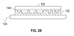
図1は、とりわけ、基板102上の膜を平坦化するために使用され得る装置100を示している。基板102は、基板チャック104に結合されてもよい。基板チャック104は真空チャック、ピン型チャック、溝型チャック、静電チャック、電磁チャック等であってもよいが、これらに限定されない。
平坦化プロセスは、図2A-2Cに概略的に示されるステップを含む。図2Aに示すように、成形性材料124は、液滴の形態で基板102上に分配される。先に議論したように、基板表面は、トポグラフィを有し、このトポグラフィは、以前の処理操作に基づいて既知であるかもしれないし、プロファイルメータ、AFM、SEM、またはZygo NewView 8200のような光学干渉効果に基づく光学表面プロファイラプロファイルメータを使用して測定されかもしれない。堆積された成形性材料124の局所体積密度は、基板トポグラフィに応じて変化する。次に、スーパーストレート108は、成形可能なデータ124と接触するように配置される。
UVユニットとカメラユニットとの統合
しかしながら、プロセス撮像ユニットとの統合は難しい。統合のための一つの重要な要件は、UVユニット126及びカメラ136のための非干渉光路である。更に、LEDのアレイの露光強度が距離の関数として二次関数的に低下することにつれて、LED群のアレイとウェハとの間の短い距離が、ウェハ上のUV露光の効率的な強度を確保するために必要とされる。
Claims (20)
- スーパーストレートまたはテンプレートを保持するように構成された第1サイド、および、第2サイドを有するチャックと、
前記チャックの前記第2サイドから離間されたボードによって支持された複数の撮像センサと、
前記チャックと前記複数の撮像センサとの間に配置されるように前記ボードによって支持された複数の光源と、
を備え、
前記複数の撮像センサの各々は、前記複数の光源の各々に対して重ならないように配置されることを特徴とする装置。 - 前記複数の撮像センサおよび前記複数の光源の各々は、前記複数の撮像センサの各々から取得される画像と前記複数の光源からの光との干渉が最小化されるように前記チャックから特定の距離だけ離間されている、
ことを特徴とする請求項1に記載の装置。 - 前記複数の撮像センサは、前記ボードの1つの面によって支持され、前記複数の光源は、前記ボードの他の面によって支持される、
ことを特徴とする請求項1記載の装置。 - 前記チャックは、前記複数の光源の各々から射出される光を透過する、
ことを特徴とする請求項1に記載の装置。 - 前記複数の撮像センサは、可視光を測定するように構成されている、
ことを特徴とする請求項1に記載の装置。 - 前記複数の撮像センサの各々は、局所領域の画像を得るように構成されている、
ことを特徴とする請求項1に記載の装置。 - 前記複数の撮像センサの各々によって取得された画像群を単一の画像に結合するように構成された画像プロセッサを更に備える、
ことを特徴とする請求項4に記載の装置。 - 前記複数の光源は、前記チャックおよび前記スーパーストレートおよび前記テンプレートを透過するUV光を生成するように構成されている、
ことを特徴とする請求項1に記載の装置。 - 前記複数の光源は、UV発光ダイオード(LED)を含む、
ことを特徴とする請求項1に記載の装置。 - 前記複数の光源をその上に実装するための第1ボードと、
前記複数の撮像センサをその上に実装するための第2ボードと、
を更に備えることを特徴とする請求項1に記載の装置。 - 前記第1ボードは、前記複数の光源の各々の間に複数の穴を含む、
ことを特徴とする請求項10に記載の装置。 - 前記複数の撮像センサの各々が、前記複数の穴のうち対応する1つと位置合わせされている、
ことを特徴とする請求項11に記載の装置。 - 基板上に硬化性材料を堆積させる堆積工程と、
前記硬化性材料の上方に配置されたボードによって支持された複数の撮像センサを用いて、前記堆積工程で堆積された前記硬化性材料の複数の局所画像を取得する取得工程と、
前記硬化性材料と前記複数の撮像センサとの間に配置されように前記ボードによって支持された複数の光源からの光で前記硬化性材料を照射することによって前記硬化性材料を硬化させる硬化工程と、
を含み、
前記複数の撮像センサの各々は、前記複数の光源の各々に対して重ならないように配置されることを特徴とする硬化方法。 - 前記複数の光源によって前記硬化性材料にUVを放射することを更に含む、
ことを特徴とする請求項13に記載の硬化方法。 - 前記複数の光源は、UV発光ダイオード(LED)を含む、
ことを特徴とする請求項13に記載の硬化方法。 - 前記複数の局所画像を単一画像に処理することを更に含む、
ことを特徴とする請求項13に記載の硬化方法。 - 前記複数の撮像センサは、前記ボードの1つの面によって支持され、前記複数の光源は、前記ボードの他の面によって支持される、
ことを特徴とする請求項13に記載の硬化方法。 - 前記硬化工程を行う前に、スーパーストレートまたはテンプレートと前記硬化性材料とを接触させるように、前記スーパーストレートまたは前記テンプレートを保持するチャック、を駆動する駆動工程、
を更に含むことを特徴とする請求項13に記載の硬化方法。 - 前記チャックは、前記複数の光源から射出される光を透過する、
ことを特徴とする請求項18に記載の硬化方法。 - 物品を製造するための方法であって、
請求項13に記載の硬化方法で、基板上の硬化性材料を硬化させる硬化工程と、
前記硬化工程が行われた前記基板を処理する処理工程と、
を含み、
前記処理工程で処理された前記基板から物品を製造することを特徴とする方法。
Applications Claiming Priority (3)
| Application Number | Priority Date | Filing Date | Title |
|---|---|---|---|
| US16/696,944 | 2019-11-26 | ||
| US16/696,944 US11107678B2 (en) | 2019-11-26 | 2019-11-26 | Wafer process, apparatus and method of manufacturing an article |
| PCT/US2020/060967 WO2021108175A1 (en) | 2019-11-26 | 2020-11-18 | Wafer process, apparatus and method of manufacturing an article |
Publications (2)
| Publication Number | Publication Date |
|---|---|
| JP2023501765A JP2023501765A (ja) | 2023-01-19 |
| JP7598359B2 true JP7598359B2 (ja) | 2024-12-11 |
Family
ID=75974240
Family Applications (1)
| Application Number | Title | Priority Date | Filing Date |
|---|---|---|---|
| JP2022504305A Active JP7598359B2 (ja) | 2019-11-26 | 2020-11-18 | ウェハプロセス、物品を製造する装置および方法 |
Country Status (5)
| Country | Link |
|---|---|
| US (2) | US11107678B2 (ja) |
| JP (1) | JP7598359B2 (ja) |
| KR (1) | KR102780456B1 (ja) |
| TW (1) | TWI811579B (ja) |
| WO (1) | WO2021108175A1 (ja) |
Families Citing this family (4)
| Publication number | Priority date | Publication date | Assignee | Title |
|---|---|---|---|---|
| US11562924B2 (en) * | 2020-01-31 | 2023-01-24 | Canon Kabushiki Kaisha | Planarization apparatus, planarization process, and method of manufacturing an article |
| US12027373B2 (en) * | 2021-05-28 | 2024-07-02 | Canon Kabushiki Kaisha | Planarization process, planarization system, and method of manufacturing an article |
| CN113683052B (zh) * | 2021-09-14 | 2023-09-05 | 深圳清华大学研究院 | 一种超滑石墨岛移动组件的制作及使用方法 |
| US12300522B2 (en) * | 2021-12-21 | 2025-05-13 | Canon Kabushiki Kaisha | Apparatus including a substrate chuck, a dispenser, and a planarization head and methods of using the same |
Citations (7)
| Publication number | Priority date | Publication date | Assignee | Title |
|---|---|---|---|---|
| JP2008183810A (ja) | 2007-01-30 | 2008-08-14 | Toshiba Mach Co Ltd | 転写方法及び装置 |
| JP2011071191A (ja) | 2009-09-24 | 2011-04-07 | Toshiba Mach Co Ltd | 転写装置および転写方法 |
| JP2013069918A (ja) | 2011-09-22 | 2013-04-18 | Toshiba Corp | インプリント方法およびインプリント装置 |
| JP2013168504A (ja) | 2012-02-15 | 2013-08-29 | Toshiba Corp | インプリント装置およびインプリント方法 |
| JP2017038042A (ja) | 2015-08-10 | 2017-02-16 | キヤノン株式会社 | インプリント装置、および物品の製造方法 |
| JP2017103451A (ja) | 2015-11-24 | 2017-06-08 | キヤノン株式会社 | インプリント装置、インプリント方法、および物品の製造方法 |
| JP2019186532A (ja) | 2018-03-30 | 2019-10-24 | キヤノン株式会社 | ディスペンサの性能特性を用いて液滴の物理的属性の変動を低減するための方法および装置 |
Family Cites Families (15)
| Publication number | Priority date | Publication date | Assignee | Title |
|---|---|---|---|---|
| JP2000356957A (ja) * | 1999-06-15 | 2000-12-26 | Fuji Xerox Co Ltd | 導電性カラーフィルタ、その製造方法、製造装置及び液晶表示素子 |
| US7684095B2 (en) | 2004-09-27 | 2010-03-23 | Lexmark International, Inc. | Scanning apparatus having an ultraviolet light source |
| JP4356113B2 (ja) * | 2005-08-08 | 2009-11-04 | セイコーエプソン株式会社 | 製膜方法、パターニング方法、光学装置の製造方法、および電子装置の製造方法 |
| KR101101132B1 (ko) | 2007-11-23 | 2012-01-12 | 삼성엘이디 주식회사 | 발광소자 검사장치 및 이를 이용한 발광소자 검사방법 |
| JP2009194519A (ja) | 2008-02-13 | 2009-08-27 | Pfu Ltd | 画像読取装置 |
| KR100990641B1 (ko) | 2008-06-04 | 2010-10-29 | 삼성엘이디 주식회사 | Led 검사 장치 및 그 방법 |
| JP5897090B2 (ja) | 2013-10-22 | 2016-03-30 | キヤノン・コンポーネンツ株式会社 | イメージセンサユニット、画像読取装置および紙葉類識別装置 |
| US20180294294A1 (en) | 2015-11-06 | 2018-10-11 | Silicon Display Technology | Flat plate type of image sensor |
| JP6685821B2 (ja) | 2016-04-25 | 2020-04-22 | キヤノン株式会社 | 計測装置、インプリント装置、物品の製造方法、光量決定方法、及び、光量調整方法 |
| US10410892B2 (en) * | 2016-11-18 | 2019-09-10 | Taiwan Semiconductor Manufacturing Company Ltd. | Method of semiconductor wafer bonding and system thereof |
| DE102017206429A1 (de) * | 2017-04-13 | 2018-10-18 | Fraunhofer-Gesellschaft zur Förderung der angewandten Forschung e.V. | Multiaperturabbildungsvorrichtung, Abbildungssystem und Verfahren zum Bereitstellen einer Multiaperturabbildungsvorrichtung |
| JP7005369B2 (ja) * | 2018-02-05 | 2022-01-21 | キオクシア株式会社 | 薬液塗布装置および半導体デバイスの製造方法 |
| US11631652B2 (en) * | 2019-01-15 | 2023-04-18 | Taiwan Semiconductor Manufacturing Company Ltd. | Method and apparatus for bonding semiconductor substrate |
| US10801969B1 (en) * | 2019-09-12 | 2020-10-13 | Lumentum Operations Llc | Testing device for bottom-emitting or bottom-detecting optical devices |
| JP2022144930A (ja) * | 2021-03-19 | 2022-10-03 | キオクシア株式会社 | インプリント方法および半導体装置の製造方法 |
-
2019
- 2019-11-26 US US16/696,944 patent/US11107678B2/en active Active
-
2020
- 2020-11-03 TW TW109138243A patent/TWI811579B/zh active
- 2020-11-18 JP JP2022504305A patent/JP7598359B2/ja active Active
- 2020-11-18 WO PCT/US2020/060967 patent/WO2021108175A1/en not_active Ceased
- 2020-11-18 KR KR1020227020449A patent/KR102780456B1/ko active Active
-
2021
- 2021-07-28 US US17/387,243 patent/US12176208B2/en active Active
Patent Citations (7)
| Publication number | Priority date | Publication date | Assignee | Title |
|---|---|---|---|---|
| JP2008183810A (ja) | 2007-01-30 | 2008-08-14 | Toshiba Mach Co Ltd | 転写方法及び装置 |
| JP2011071191A (ja) | 2009-09-24 | 2011-04-07 | Toshiba Mach Co Ltd | 転写装置および転写方法 |
| JP2013069918A (ja) | 2011-09-22 | 2013-04-18 | Toshiba Corp | インプリント方法およびインプリント装置 |
| JP2013168504A (ja) | 2012-02-15 | 2013-08-29 | Toshiba Corp | インプリント装置およびインプリント方法 |
| JP2017038042A (ja) | 2015-08-10 | 2017-02-16 | キヤノン株式会社 | インプリント装置、および物品の製造方法 |
| JP2017103451A (ja) | 2015-11-24 | 2017-06-08 | キヤノン株式会社 | インプリント装置、インプリント方法、および物品の製造方法 |
| JP2019186532A (ja) | 2018-03-30 | 2019-10-24 | キヤノン株式会社 | ディスペンサの性能特性を用いて液滴の物理的属性の変動を低減するための方法および装置 |
Also Published As
| Publication number | Publication date |
|---|---|
| US12176208B2 (en) | 2024-12-24 |
| TW202133947A (zh) | 2021-09-16 |
| TWI811579B (zh) | 2023-08-11 |
| JP2023501765A (ja) | 2023-01-19 |
| US20210358746A1 (en) | 2021-11-18 |
| KR102780456B1 (ko) | 2025-03-14 |
| WO2021108175A1 (en) | 2021-06-03 |
| US20210159075A1 (en) | 2021-05-27 |
| US11107678B2 (en) | 2021-08-31 |
| KR20220100690A (ko) | 2022-07-15 |
Similar Documents
| Publication | Publication Date | Title |
|---|---|---|
| JP7598359B2 (ja) | ウェハプロセス、物品を製造する装置および方法 | |
| TWI426353B (zh) | 壓印微影系統及壓印方法 | |
| US11776840B2 (en) | Superstrate chuck, method of use, and method of manufacturing an article | |
| JP6940944B2 (ja) | インプリント装置、及び物品製造方法 | |
| US12283522B2 (en) | Planarization apparatus, planarization process, and method of manufacturing an article | |
| JP2021034723A (ja) | 平坦化方法、平坦化装置及び物品製造方法 | |
| JP2020074446A (ja) | インプリント装置、及び、物品の製造方法 | |
| US11443940B2 (en) | Apparatus for uniform light intensity and methods of using the same | |
| JP2021135504A (ja) | 均一光強度のための露光装置及びその使用方法 | |
| JP7071484B2 (ja) | インプリントシステム内のディストーションの補正を伴うナノ製作方法 | |
| US20240145269A1 (en) | Planarization process, planarization system and method of manufacturing an article | |
| US10976657B2 (en) | System and method for illuminating edges of an imprint field with a gradient dosage | |
| JP2019216143A (ja) | 型を用いて基板上の組成物を成形する成形装置、および物品の製造方法 | |
| US11664220B2 (en) | Edge exclusion apparatus and methods of using the same | |
| JP6951483B2 (ja) | 質量速度変動フィーチャを有するテンプレート、テンプレートを使用するナノインプリントリソグラフィ装置、およびテンプレートを使用する方法 | |
| US20220102156A1 (en) | Planarization apparatus, planarization process, and method of manufacturing an article | |
| US11972976B2 (en) | Planarization system, planarization process, and method of manufacturing an article | |
| KR102294079B1 (ko) | 임프린트 방법, 임프린트 장치 및 물품의 제조 방법 | |
| US20240321586A1 (en) | Planarization process, planarization system, and method of manufacturing an article | |
| KR20230043723A (ko) | 표면 성형 방법, 성형 시스템, 및 물품 제조 방법 | |
| JP2020145354A (ja) | 平坦化装置、平坦化方法及び物品の製造方法 |
Legal Events
| Date | Code | Title | Description |
|---|---|---|---|
| A621 | Written request for application examination |
Free format text: JAPANESE INTERMEDIATE CODE: A621 Effective date: 20230814 |
|
| A977 | Report on retrieval |
Free format text: JAPANESE INTERMEDIATE CODE: A971007 Effective date: 20240731 |
|
| A131 | Notification of reasons for refusal |
Free format text: JAPANESE INTERMEDIATE CODE: A131 Effective date: 20240816 |
|
| A521 | Request for written amendment filed |
Free format text: JAPANESE INTERMEDIATE CODE: A523 Effective date: 20241008 |
|
| TRDD | Decision of grant or rejection written | ||
| A01 | Written decision to grant a patent or to grant a registration (utility model) |
Free format text: JAPANESE INTERMEDIATE CODE: A01 Effective date: 20241101 |
|
| A61 | First payment of annual fees (during grant procedure) |
Free format text: JAPANESE INTERMEDIATE CODE: A61 Effective date: 20241129 |
|
| R150 | Certificate of patent or registration of utility model |
Ref document number: 7598359 Country of ref document: JP Free format text: JAPANESE INTERMEDIATE CODE: R150 |