JP7580552B2 - Semiconductor Device - Google Patents
Semiconductor Device Download PDFInfo
- Publication number
- JP7580552B2 JP7580552B2 JP2023175809A JP2023175809A JP7580552B2 JP 7580552 B2 JP7580552 B2 JP 7580552B2 JP 2023175809 A JP2023175809 A JP 2023175809A JP 2023175809 A JP2023175809 A JP 2023175809A JP 7580552 B2 JP7580552 B2 JP 7580552B2
- Authority
- JP
- Japan
- Prior art keywords
- transistor
- drain
- electrically connected
- source
- gate
- Prior art date
- Legal status (The legal status is an assumption and is not a legal conclusion. Google has not performed a legal analysis and makes no representation as to the accuracy of the status listed.)
- Active
Links
Images


Classifications
-
- H—ELECTRICITY
- H10—SEMICONDUCTOR DEVICES; ELECTRIC SOLID-STATE DEVICES NOT OTHERWISE PROVIDED FOR
- H10W—GENERIC PACKAGES, INTERCONNECTIONS, CONNECTORS OR OTHER CONSTRUCTIONAL DETAILS OF DEVICES COVERED BY CLASS H10
- H10W90/00—Package configurations
-
- G—PHYSICS
- G02—OPTICS
- G02F—OPTICAL DEVICES OR ARRANGEMENTS FOR THE CONTROL OF LIGHT BY MODIFICATION OF THE OPTICAL PROPERTIES OF THE MEDIA OF THE ELEMENTS INVOLVED THEREIN; NON-LINEAR OPTICS; FREQUENCY-CHANGING OF LIGHT; OPTICAL LOGIC ELEMENTS; OPTICAL ANALOGUE/DIGITAL CONVERTERS
- G02F1/00—Devices or arrangements for the control of the intensity, colour, phase, polarisation or direction of light arriving from an independent light source, e.g. switching, gating or modulating; Non-linear optics
- G02F1/01—Devices or arrangements for the control of the intensity, colour, phase, polarisation or direction of light arriving from an independent light source, e.g. switching, gating or modulating; Non-linear optics for the control of the intensity, phase, polarisation or colour
- G02F1/13—Devices or arrangements for the control of the intensity, colour, phase, polarisation or direction of light arriving from an independent light source, e.g. switching, gating or modulating; Non-linear optics for the control of the intensity, phase, polarisation or colour based on liquid crystals, e.g. single liquid crystal display cells
- G02F1/133—Constructional arrangements; Operation of liquid crystal cells; Circuit arrangements
- G02F1/136—Liquid crystal cells structurally associated with a semi-conducting layer or substrate, e.g. cells forming part of an integrated circuit
- G02F1/1362—Active matrix addressed cells
-
- G—PHYSICS
- G09—EDUCATION; CRYPTOGRAPHY; DISPLAY; ADVERTISING; SEALS
- G09G—ARRANGEMENTS OR CIRCUITS FOR CONTROL OF INDICATING DEVICES USING STATIC MEANS TO PRESENT VARIABLE INFORMATION
- G09G3/00—Control arrangements or circuits, of interest only in connection with visual indicators other than cathode-ray tubes
- G09G3/20—Control arrangements or circuits, of interest only in connection with visual indicators other than cathode-ray tubes for presentation of an assembly of a number of characters, e.g. a page, by composing the assembly by combination of individual elements arranged in a matrix no fixed position being assigned to or needed to be assigned to the individual characters or partial characters
- G09G3/34—Control arrangements or circuits, of interest only in connection with visual indicators other than cathode-ray tubes for presentation of an assembly of a number of characters, e.g. a page, by composing the assembly by combination of individual elements arranged in a matrix no fixed position being assigned to or needed to be assigned to the individual characters or partial characters by control of light from an independent source
- G09G3/36—Control arrangements or circuits, of interest only in connection with visual indicators other than cathode-ray tubes for presentation of an assembly of a number of characters, e.g. a page, by composing the assembly by combination of individual elements arranged in a matrix no fixed position being assigned to or needed to be assigned to the individual characters or partial characters by control of light from an independent source using liquid crystals
- G09G3/3611—Control of matrices with row and column drivers
- G09G3/3674—Details of drivers for scan electrodes
- G09G3/3677—Details of drivers for scan electrodes suitable for active matrices only
-
- G—PHYSICS
- G11—INFORMATION STORAGE
- G11C—STATIC STORES
- G11C19/00—Digital stores in which the information is moved stepwise, e.g. shift registers
- G11C19/28—Digital stores in which the information is moved stepwise, e.g. shift registers using semiconductor elements
-
- G—PHYSICS
- G09—EDUCATION; CRYPTOGRAPHY; DISPLAY; ADVERTISING; SEALS
- G09G—ARRANGEMENTS OR CIRCUITS FOR CONTROL OF INDICATING DEVICES USING STATIC MEANS TO PRESENT VARIABLE INFORMATION
- G09G2310/00—Command of the display device
- G09G2310/02—Addressing, scanning or driving the display screen or processing steps related thereto
- G09G2310/0264—Details of driving circuits
- G09G2310/0286—Details of a shift registers arranged for use in a driving circuit
-
- H—ELECTRICITY
- H10—SEMICONDUCTOR DEVICES; ELECTRIC SOLID-STATE DEVICES NOT OTHERWISE PROVIDED FOR
- H10D—INORGANIC ELECTRIC SEMICONDUCTOR DEVICES
- H10D86/00—Integrated devices formed in or on insulating or conducting substrates, e.g. formed in silicon-on-insulator [SOI] substrates or on stainless steel or glass substrates
- H10D86/40—Integrated devices formed in or on insulating or conducting substrates, e.g. formed in silicon-on-insulator [SOI] substrates or on stainless steel or glass substrates characterised by multiple TFTs
- H10D86/421—Integrated devices formed in or on insulating or conducting substrates, e.g. formed in silicon-on-insulator [SOI] substrates or on stainless steel or glass substrates characterised by multiple TFTs having a particular composition, shape or crystalline structure of the active layer
- H10D86/423—Integrated devices formed in or on insulating or conducting substrates, e.g. formed in silicon-on-insulator [SOI] substrates or on stainless steel or glass substrates characterised by multiple TFTs having a particular composition, shape or crystalline structure of the active layer comprising semiconductor materials not belonging to the Group IV, e.g. InGaZnO
-
- H—ELECTRICITY
- H10—SEMICONDUCTOR DEVICES; ELECTRIC SOLID-STATE DEVICES NOT OTHERWISE PROVIDED FOR
- H10D—INORGANIC ELECTRIC SEMICONDUCTOR DEVICES
- H10D86/00—Integrated devices formed in or on insulating or conducting substrates, e.g. formed in silicon-on-insulator [SOI] substrates or on stainless steel or glass substrates
- H10D86/40—Integrated devices formed in or on insulating or conducting substrates, e.g. formed in silicon-on-insulator [SOI] substrates or on stainless steel or glass substrates characterised by multiple TFTs
- H10D86/60—Integrated devices formed in or on insulating or conducting substrates, e.g. formed in silicon-on-insulator [SOI] substrates or on stainless steel or glass substrates characterised by multiple TFTs wherein the TFTs are in active matrices
Landscapes
- Physics & Mathematics (AREA)
- Engineering & Computer Science (AREA)
- General Physics & Mathematics (AREA)
- Chemical & Material Sciences (AREA)
- Crystallography & Structural Chemistry (AREA)
- Nonlinear Science (AREA)
- Theoretical Computer Science (AREA)
- Computer Hardware Design (AREA)
- Microelectronics & Electronic Packaging (AREA)
- Optics & Photonics (AREA)
- Mathematical Physics (AREA)
- Control Of Indicators Other Than Cathode Ray Tubes (AREA)
- Shift Register Type Memory (AREA)
- Liquid Crystal (AREA)
- Liquid Crystal Display Device Control (AREA)
- Thin Film Transistor (AREA)
- Devices For Indicating Variable Information By Combining Individual Elements (AREA)
- Control Of El Displays (AREA)
- Electronic Switches (AREA)
- Logic Circuits (AREA)
- Condensed Matter Physics & Semiconductors (AREA)
- Metal-Oxide And Bipolar Metal-Oxide Semiconductor Integrated Circuits (AREA)
- Design And Manufacture Of Integrated Circuits (AREA)
Description
本発明の一態様は、半導体装置、及び該半導体装置を有する表示装置に関する。特に、順
序回路、及び該順序回路を有するシフトレジスタ等の半導体装置に関する。
1. Field of the Invention One embodiment of the present invention relates to a semiconductor device and a display device including the semiconductor device, and in particular to a semiconductor device such as a sequential circuit and a shift register including the sequential circuit.
近年、同じ極性のトランジスタで構成される順序回路の開発が活発に進められている。特
に、特許文献1には、トランジスタの特性変化を抑制することができる順序回路が開示さ
れている。
In recent years, development of sequential circuits composed of transistors of the same polarity has been actively promoted. In particular,
図17(A)は、従来の順序回路の構成を示す。従来の順序回路は、トランジスタT13
と、並列に接続されたトランジスタT14及びトランジスタT15と、を有する。従来の
順序回路では、トランジスタT13がオンになり、トランジスタT14及びトランジスタ
T15がオフになることで、第1クロック信号C1を出力している。第1クロック信号C
1がハイレベルであれば、第1スキャン信号Vg1がハイレベルになる(図17(B)参
照)。そして、奇数フレームでは、トランジスタT13がオフになり、トランジスタT1
4がオンになり、トランジスタT15がオフになることで、第1供給電圧VSSを出力し
ている(図17(C)参照)。また、偶数フレームでは、トランジスタT13がオフにな
り、トランジスタT14がオフになり、トランジスタT15がオンになることで、第1供
給電圧VSSを出力している(図17(D)参照)。このように、奇数フレームではトラ
ンジスタT15をオフにし、偶数フレームではトランジスタT14をオフにすることで、
トランジスタT14及びトランジスタT15の特性変化が抑制される。
FIG. 17A shows the configuration of a conventional sequential circuit. The conventional sequential circuit includes a transistor T13.
In the conventional sequential circuit, the transistor T13 is turned on and the transistors T14 and T15 are turned off to output the first clock signal C1.
If the first scan signal Vg1 is at a high level, the first scan signal Vg1 is at a high level (see FIG. 17B). Then, in an odd-numbered frame, the transistor T13 is turned off and the transistor T1
In the even-numbered frames, transistor T13 is turned off, transistor T14 is turned off, and transistor T15 is turned on, thereby outputting the first supply voltage VSS (see FIG. 17(C)). Also, in the even-numbered frames, transistor T13 is turned off, transistor T14 is turned off, and transistor T15 is turned on, thereby outputting the first supply voltage VSS (see FIG. 17(D)). In this way, by turning off transistor T15 in odd-numbered frames and turning off transistor T14 in even-numbered frames,
Changes in the characteristics of the transistors T14 and T15 are suppressed.
しかしながら、従来の順序回路では、並列に接続された二つのトランジスタの一方をオフ
にし、他方のトランジスタのみを駆動させるため、並列に接続された二つのトランジスタ
のそれぞれに十分な駆動能力が求められる。よって、トランジスタのW(Wはチャネル幅
)/L(Lはチャネル長)が大きくなるといった問題があった。また、トランジスタのW
/Lが十分に大きくなければ、出力信号の変化がゆるやかになり、出力信号に遅延やなま
りが生じるといった問題があった。
However, in a conventional sequential circuit, one of two transistors connected in parallel is turned off and only the other transistor is driven, so each of the two transistors connected in parallel is required to have sufficient driving capability. This causes a problem that the W (W is the channel width)/L (L is the channel length) ratio of the transistor becomes large.
If /L is not sufficiently large, the change in the output signal becomes gradual, causing problems such as delays and distortions in the output signal.
そこで、本発明の一態様は、トランジスタの特性変化を抑制するとともに、トランジスタ
のW/Lを大きくすることなく、出力信号を急峻に変化させることができる半導体装置を
提供することを課題の一とする。また、本発明の一態様は、新規の回路構成を含む半導体
装置を提供することを課題の一とする。なお、これらの課題の記載は、他の課題の存在を
妨げるものではない。なお、本発明の一態様は、これらの課題の全てを解決する必要はな
いものとする。なお、これら以外の課題は、明細書、図面、請求項などの記載から、自ず
と明らかとなるものであり、明細書、図面、請求項などの記載から、これら以外の課題を
抽出することが可能である。
In view of the above, an object of one embodiment of the present invention is to provide a semiconductor device that can suppress changes in transistor characteristics and can rapidly change an output signal without increasing the W/L of the transistor. Another object of one embodiment of the present invention is to provide a semiconductor device including a novel circuit configuration. Note that the description of these objects does not prevent the existence of other objects. Note that one embodiment of the present invention does not need to solve all of these objects. Note that objects other than these objects will become apparent from descriptions in the specification, drawings, claims, and the like, and other objects can be extracted from descriptions in the specification, drawings, claims, and the like.
本発明の一態様は、ソース又はドレインの一方に第1の信号が入力された第1のトランジ
スタと、ソース又はドレインの一方に第1の電位が入力され、ソース又はドレインの他方
が第1のトランジスタのソース又はドレインの他方と電気的に接続された第2のトランジ
スタと、ソース又はドレインの一方が第2のトランジスタのソース又はドレインの一方と
電気的に接続され、ソース又はドレインの他方が第1のトランジスタのソース又はドレイ
ンの他方と電気的に接続された第3のトランジスタと、第1のトランジスタ、第2のトラ
ンジスタ及び第3のトランジスタのオン又はオフを制御する手段と、を有する半導体装置
の駆動方法である。そして、当該半導体装置は、第1の信号を第1のトランジスタを介し
て出力する第1のステップと、第1の電位を第2のトランジスタ及び第3のトランジスタ
を介して出力する第2のステップと、第1の電位を第2のトランジスタを介して出力する
第3のステップと、を有する第1の期間と、第1の信号を第1のトランジスタを介して出
力する第4のステップと、第1の電位を第2のトランジスタ及び第3のトランジスタを介
して出力する第5のステップと、第1の電位を第3のトランジスタを介して出力する第6
のステップと、を有する第2の期間と、を順に繰り返す。
One embodiment of the present invention is a method for driving a semiconductor device including: a first transistor having a first signal input to one of its source or drain; a second transistor having a first potential input to one of its source or drain and the other of its source or drain electrically connected to the other of the source or drain of the first transistor; a third transistor having one of its source or drain electrically connected to the one of the source or drain of the second transistor and the other of its source or drain electrically connected to the other of the source or drain of the first transistor; and means for controlling on/off of the first transistor, the second transistor, and the third transistor. The semiconductor device includes a first period having a first step of outputting a first signal through a first transistor, a second step of outputting the first potential through a second transistor and a third transistor, and a third step of outputting the first potential through the second transistor, a fourth step of outputting the first signal through the first transistor, a fifth step of outputting the first potential through the second transistor and the third transistor, and a sixth step of outputting the first potential through the third transistor.
and a second period having the steps of:
上記本発明の一態様は、第1の期間において、第1のステップ、第2のステップ及び第3
のステップのそれぞれを2回以上行い、第2の期間において、第4のステップ、第5のス
テップ及び第6のステップのそれぞれを2回以上行ってもよい。また、上記本発明の一態
様は、第2のトランジスタのチャネル幅は、第3のトランジスタのチャネル幅の90%以
上、110%以下であってもよい。また、上記本発明の一態様において、第1のトランジ
スタのチャネル幅は、第2のトランジスタのチャネル幅よりも大きく、且つ第3のトラン
ジスタのチャネル幅よりも大きくてもよい。
In one aspect of the present invention, a first step, a second step, and a third step are performed in a first period.
and in the second period, each of the fourth step, the fifth step, and the sixth step may be performed two or more times. In the above embodiment of the present invention, the channel width of the second transistor may be greater than or equal to 90% and less than or equal to 110% of the channel width of the third transistor. In the above embodiment of the present invention, the channel width of the first transistor may be greater than the channel width of the second transistor and greater than the channel width of the third transistor.
本発明の一態様は、ソース又はドレインの一方が第1の配線と電気的に接続され、ソース
又はドレインの他方が第2の配線と電気的に接続された第1のトランジスタと、ソース又
はドレインの一方が第1の配線と電気的に接続され、ソース又はドレインの他方が第2の
配線と電気的に接続された第2のトランジスタと、第1の端子が第1のトランジスタのゲ
ートと電気的に接続された第1のスイッチと、第1の端子が第2のトランジスタのゲート
と電気的に接続され、第2の端子が第1のスイッチの第2の端子と電気的に接続された第
2のスイッチと、第1の端子が第3の配線と電気的に接続され、第2の端子が第1のトラ
ンジスタのゲートと電気的に接続された第3のスイッチと、第1の端子が第3の配線と電
気的に接続され、第2の端子が第2のトランジスタのゲートと電気的に接続された第4の
スイッチと、を有することを特徴とする半導体装置である。
One embodiment of the present invention is a semiconductor device including: a first transistor having one of a source or a drain electrically connected to a first wiring and the other of the source or the drain electrically connected to a second wiring; a second transistor having one of a source or a drain electrically connected to the first wiring and the other of the source or the drain electrically connected to a second wiring; a first switch having a first terminal electrically connected to a gate of the first transistor; a second switch having a first terminal electrically connected to a gate of the second transistor and a second terminal electrically connected to a second terminal of the first switch; a third switch having a first terminal electrically connected to a third wiring and a second terminal electrically connected to a gate of the first transistor; and a fourth switch having a first terminal electrically connected to the third wiring and a second terminal electrically connected to a gate of the second transistor.
上記本発明の一態様は、ソース又はドレインの一方が第4の配線と接続され、ソース又は
ドレインの他方が第1のスイッチの第2の端子と接続され、ゲートが第4の配線と接続さ
れた第3のトランジスタと、ソース又はドレインの一方が第2の配線と接続され、ソース
又はドレインの他方が第1のスイッチの第2の端子と接続された第4のトランジスタと、
を有していてもよい。また、上記本発明の一態様は、第1のスイッチ及び第4のスイッチ
がオンであり、第2のスイッチ及び第3のスイッチがオフである第1の期間と、第1のス
イッチ及び第4のスイッチがオフであり、第2のスイッチ及び第3のスイッチがオンであ
る第2の期間と、を有していてもよい。
One embodiment of the present invention includes a third transistor having a source or a drain connected to a fourth wiring, the other of the source or the drain connected to a second terminal of a first switch, and a gate connected to the fourth wiring; a fourth transistor having a source or a drain connected to the second wiring and the other of the source or the drain connected to the second terminal of the first switch;
The above-described embodiment of the present invention may include a first period in which the first switch and the fourth switch are on and the second switch and the third switch are off, and a second period in which the first switch and the fourth switch are off and the second switch and the third switch are on.
本発明の一態様は、トランジスタの特性変化を抑制することができるとともに、トランジ
スタのW/Lを大きくすることなく、出力信号の変化を急峻にすることができる半導体装
置を提供することができる。また、本発明の一態様は、新規の回路構成を含む半導体装置
を提供することができる。
According to one embodiment of the present invention, a semiconductor device can be provided that can suppress changes in transistor characteristics and can make an output signal change sharper without increasing the W/L of the transistor.
以下では、本発明の実施の形態について図面を用いて詳細に説明する。ただし、本発明は
以下の説明に限定されず、本発明の趣旨及びその範囲から逸脱することなくその形態及び
詳細を様々に変更し得ることは、当業者であれば容易に理解される。したがって、本発明
は、以下に示す実施の形態の記載内容に限定して解釈されるものではない。
Hereinafter, the embodiments of the present invention will be described in detail with reference to the drawings. However, the present invention is not limited to the following description, and it is easily understood by those skilled in the art that the form and details of the present invention can be modified in various ways without departing from the spirit and scope of the present invention. Therefore, the present invention should not be interpreted as being limited to the description of the embodiments shown below.
なお、本発明は、集積回路、RFタグ、表示装置など、トランジスタを用いたあらゆる半
導体装置を、その範疇に含む。なお、集積回路には、マイクロプロセッサ、画像処理回路
、DSP(Digital Signal Processor)、マイクロコントロー
ラを含むLSI(Large Scale Integrated Circuit)、
FPGA(Field Programmable Gate Array)やCPLD
(Complex PLD)などのプログラマブル論理回路(PLD:Programm
able Logic Device)が、その範疇に含まれる。また、表示装置には、
液晶表示装置、有機発光素子(OLED)に代表される発光素子を各画素に備えた発光装
置、電子ペーパー、DMD(Digital Micromirror Device)
、PDP(Plasma Display Panel)、FED(Field Emi
ssion Display)などが、その範疇に含まれる。
The present invention includes in its category all semiconductor devices using transistors, such as integrated circuits, RF tags, and display devices. The integrated circuits include LSIs (Large Scale Integrated Circuits) including microprocessors, image processing circuits, DSPs (Digital Signal Processors), and microcontrollers,
FPGA (Field Programmable Gate Array) and CPLD
Programmable logic circuits (PLDs) such as Complex PLDs
The display device includes, for example, a display device with a display function, a display device with a display unit ...
Liquid crystal display devices, light-emitting devices in which each pixel has a light-emitting element such as an organic light-emitting diode (OLED), electronic paper, and DMD (Digital Micromirror Device)
, PDP (Plasma Display Panel), FED (Field Emi
Examples of such products include digital still cameras, motion display cameras, and other video display devices.
なお、本明細書において表示装置とは、液晶素子や発光素子などの表示素子が各画素に形
成されたパネルと、該パネルにコントローラを含むIC等を実装した状態にあるモジュー
ルとを、その範疇に含む。
In this specification, the term "display device" includes within its category a panel in which display elements such as liquid crystal elements or light-emitting elements are formed in each pixel, and a module in which an IC including a controller is mounted on the panel.
なお、本明細書において接続とは電気的な接続を意味しており、電流、電圧または電位が
、供給可能、或いは伝送可能な状態に相当する。従って、接続している状態とは、直接接
続している状態を必ずしも指すわけではなく、電流、電圧または電位が、供給可能、或い
は伝送可能であるように、配線、抵抗、ダイオード、トランジスタなどの回路素子を介し
て間接的に接続している状態も、その範疇に含む。また、回路図上は独立している構成要
素どうしが接続されている場合であっても、実際には、例えば配線の一部が電極として機
能する場合など、一の導電膜が、複数の構成要素の機能を併せ持っている場合もある。本
明細書において接続とは、このような、一の導電膜が、複数の構成要素の機能を併せ持っ
ている場合も、その範疇に含める。
In this specification, the term "connection" means electrical connection, and corresponds to a state in which a current, voltage, or potential can be supplied or transmitted. Therefore, the state of being connected does not necessarily refer to a state of being directly connected, but also includes a state of being indirectly connected via a circuit element such as a wiring, a resistor, a diode, or a transistor so that a current, voltage, or potential can be supplied or transmitted. Even if components that are independent on a circuit diagram are connected to each other, in reality, one conductive film may have the functions of multiple components, for example, when a part of the wiring functions as an electrode. In this specification, the term "connection" also includes such a case in which one conductive film has the functions of multiple components.
なお、トランジスタのソースとは、活性層として機能する半導体膜の一部であるソース領
域、或いは上記半導体膜に接続されたソース電極を意味する。同様に、トランジスタのド
レインとは、上記半導体膜の一部であるドレイン領域、或いは上記半導体膜に接続された
ドレイン電極を意味する。また、ゲートはゲート電極を意味する。
The source of a transistor means a source region that is a part of the semiconductor film that functions as an active layer, or a source electrode connected to the semiconductor film. Similarly, the drain of a transistor means a drain region that is a part of the semiconductor film, or a drain electrode connected to the semiconductor film. Furthermore, the gate means a gate electrode.
なお、トランジスタが有するソースとドレインは、トランジスタの極性及び各端子に与え
られる電位の高低によって、その呼び方が入れ替わる。一般的に、nチャネル型トランジ
スタでは、低い電位が与えられる端子がソースと呼ばれ、高い電位が与えられる端子がド
レインと呼ばれる。また、pチャネル型トランジスタでは、低い電位が与えられる端子が
ドレインと呼ばれ、高い電位が与えられる端子がソースと呼ばれる。本明細書では、便宜
上、ソースとドレインとが固定されているものと仮定して、トランジスタの接続関係を説
明する場合があるが、実際には上記電位の関係に従ってソースとドレインの呼び方が入れ
替わる。
Note that the names of the source and drain of a transistor are interchangeable depending on the polarity of the transistor and the level of the potential applied to each terminal. In general, in an n-channel transistor, a terminal to which a low potential is applied is called a source, and a terminal to which a high potential is applied is called a drain. In addition, in a p-channel transistor, a terminal to which a low potential is applied is called a drain, and a terminal to which a high potential is applied is called a source. In this specification, for convenience, the connection relationship of a transistor may be described assuming that the source and drain are fixed, but in reality, the names of the source and drain are interchangeable according to the above-mentioned potential relationship.
(実施の形態1)
本実施の形態では、本発明の一態様に係る順序回路(半導体装置ともいう)について説明
する。
(Embodiment 1)
In this embodiment, a sequential circuit (also referred to as a semiconductor device) according to one embodiment of the present invention will be described.
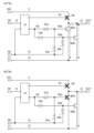
図1(A)は、本実施の形態の順序回路を示す。図1(A)の順序回路は、トランジスタ
M1、トランジスタM2a、トランジスタM2b、スイッチS3a、スイッチS3b、ス
イッチS4a、スイッチS4b、及び回路10を有する。
1A illustrates a sequential circuit according to this embodiment. The sequential circuit in FIG. 1A includes a transistor M1, a transistor M2a, a transistor M2b, a switch S3a, a switch S3b, a switch S4a, a switch S4b, and a
トランジスタM1は、第1の端子(ソース又はドレインの一方ともいう)が配線11と接
続され、第2の端子(ソース又はドレインの他方ともいう)が配線12と接続され、ゲー
トがノードN1と接続される。トランジスタM2aは、第1の端子が配線13と接続され
、第2の端子が配線12と接続され、ゲートがノードN2aと接続される。トランジスタ
M2bは、第1の端子が配線13と接続され、第2の端子が配線12と接続され、ゲート
がノードN2bと接続される。スイッチS3aは、第1の端子がノードN3と接続され、
第2の端子がノードN2aと接続される。スイッチS3bは、第1の端子がノードN3と
接続され、第2の端子がノードN2bと接続される。スイッチS4aは、第1の端子が配
線14と接続され、第2の端子がノードN2aと接続される。スイッチS4bは、第1の
端子が配線14と接続され、第2の端子がノードN2bと接続される。回路10は、第1
の端子が配線15と接続され、第2の端子が配線14と接続され、第3の端子がノードN
1と接続され、第4の端子がノードN3と接続される。
The transistor M1 has a first terminal (also referred to as one of a source and a drain) connected to a
The first terminal of the switch S4a is connected to the
The first terminal is connected to the
1 and the fourth terminal is connected to a node N3.
回路10は、ノードN1にトランジスタM1のオン又はオフを制御するための電位を供給
する機能を有する。具体的には、回路10は、ノードN1にトランジスタM1がオンにな
る電位を供給した後、ノードN1を浮遊状態とする機能を有する。また、回路10は、ノ
ードN1にトランジスタM1がオフになる電位を供給する機能を有する。さらに、回路1
0は、ノードN3にトランジスタM2a又はトランジスタM2bのオン又はオフを制御す
るための電位を供給する機能を有する。具体的には、回路10は、ノードN3にトランジ
スタM2a又はトランジスタM2bがオンになる電位を供給する機能を有する。また、回
路10は、ノードN3にトランジスタM2a又はトランジスタM2bがオフになる電位を
供給する機能を有する。なお、回路10がノードN3に供給する電位は、スイッチS3a
がオンであればノードN2aに供給され、スイッチS3bがオンであればノードN2bに
供給される。また、回路10の接続関係は、回路10の構成により適宜変更することがで
きる。
The
The
is on, the signal is supplied to node N2a, and when switch S3b is on, the signal is supplied to node N2b. The connections of the
なお、順序回路が有するトランジスタは同じ極性とする。トランジスタの極性としては、
Nチャネル型又はPチャネル型がある。本実施の形態では、便宜上、トランジスタM1、
トランジスタM2a及びトランジスタM2bをNチャネル型とする。
The transistors in the sequential circuit have the same polarity.
There are N-channel and P-channel types. In this embodiment, for convenience, the transistors M1,
The transistors M2a and M2b are N-channel types.
なお、トランジスタは、第1の端子の接続先と第2の端子の接続先との導通又は非導通を
制御する機能を有する。例えば、トランジスタM1は、配線11と配線12との導通又は
非導通を制御する機能を有する。トランジスタM2aは、配線13と配線12との導通又
は非導通を制御する機能を有する。トランジスタM2bは、配線13と配線12との導通
又は非導通を制御する機能を有する。
Note that the transistors have a function of controlling electrical continuity or non-conduction between a connection destination of the first terminal and a connection destination of the second terminal. For example, the transistor M1 has a function of controlling electrical continuity or non-conduction between the
なお、トランジスタは、ゲートの接続先と第1の端子又は第2の端子の接続先との間の電
位差を保持する機能を有する。例えば、トランジスタM1は、配線12とノードN1との
間の電位差を保持する機能を有する。
Note that the transistor has a function of holding a potential difference between a connection destination of the gate and a connection destination of the first terminal or the second terminal of the transistor M1. For example, the transistor M1 has a function of holding a potential difference between the
なお、トランジスタをスイッチに置き換えてもよい。トランジスタの第1の端子がスイッ
チの第1の端子に対応し、トランジスタの第2の端子がスイッチの第2の端子に対応する
。例えば、トランジスタM2aを第1の端子が配線13と接続され、第2の端子が配線1
2と接続されたスイッチに置き換えてもよい。トランジスタM2bを第1の端子が配線1
3と接続され、第2の端子が配線12と接続されたスイッチに置き換えてもよい。
The transistor may be replaced with a switch. The first terminal of the transistor corresponds to the first terminal of the switch, and the second terminal of the transistor corresponds to the second terminal of the switch. For example, the first terminal of the transistor M2a is connected to the
The first terminal of the transistor M2b may be replaced with a switch connected to the
3 and a switch having a first terminal connected to
なお、配線には信号又は電位等が入力され、配線は入力された信号又は電位等を伝達する
機能を有する。例えば、配線11の信号又は電位は、配線12の電位を上昇させる機能を
有することが好ましい。配線13の信号又は電位は、配線12の電位を下降させる機能を
有することが好ましい。配線14は、トランジスタM2aのオン若しくはオフを制御する
機能、トランジスタM2bのオン若しくはオフを制御する機能、又は回路10を制御する
機能を有することが好ましい。配線15の信号又は電位は、回路10を制御する機能を有
することが好ましい。
Note that a signal, a potential, or the like is input to the wiring, and the wiring has a function of transmitting the input signal, potential, or the like. For example, the signal or potential of the
本実施の形態では、便宜上、配線11には信号CK1(クロック信号ともいう)が入力さ
れ、配線12からは信号OUT(出力信号ともいう)が出力され、配線13には電位V1
(第1の電位ともいう)が供給され、配線14には信号RE(リセット信号ともいう)が
入力され、配線15には信号SP(スタート信号ともいう)が入力されるものとする。ま
た、便宜上、信号CK1、信号SP及び信号REは、ハイレベル及びロウレベルを有する
ものとする。そして、ロウレベルの電位が電位V1であり、ハイレベルの電位が電位V2
(第2の電位ともいう)であるものとする。電位V2は電位V1よりも高い電位である。
In this embodiment, for convenience, a signal CK1 (also referred to as a clock signal) is input to the
A signal CK1 (also referred to as a first potential) is supplied to the
The potential V2 is higher than the potential V1 (also referred to as a second potential).
次に、図1(A)の順序回路の動作について説明する。 Next, we will explain the operation of the sequential circuit in Figure 1(A).
図2及び図3は、図1(A)の順序回路の動作を説明するためのタイミングチャートの一
例を示す。図2及び図3のタイミングチャートは、期間Ta及び期間Tbを有する。そし
て、図2は、期間T1a乃至期間T4aを有する期間Taのタイミングチャートを示し、
図3は、期間T1b乃至期間T4bを有する期間Tbのタイミングチャートを示す。また
、図2及び図3は、スイッチS3a及びスイッチS4bのオン又はオフの関係、スイッチ
S3b及びスイッチS4aのオン又はオフの関係、信号CK1、信号SP、信号RE、ノ
ードN1の電位VN1、ノードN2aの電位VN2a、ノードN2bの電位VN2b、並
びに信号OUTを示す。
2 and 3 are examples of timing charts for explaining the operation of the sequential circuit in FIG. 1A. The timing charts in FIG. 2 and 3 each include a period Ta and a period Tb. FIG. 2 shows a timing chart of the period Ta including periods T1a to T4a.
3 is a timing chart of a period Tb having periods T1b to T4b. 2 and 3 also show the on/off relationship of the switches S3a and S4b, the on/off relationship of the switches S3b and S4a, the signal CK1, the signal SP, the signal RE, the potential VN1 of the node N1, the potential VN2a of the node N2a, the potential VN2b of the node N2b, and the signal OUT.
図4乃至図7は、各期間(各ステップともいう)における図1(A)の順序回路の動作の
模式図を示す。図4(A)は期間T1a、図4(B)は期間T2a、図5(A)は期間T
3a、図5(B)は期間T4a、図6(A)は期間T1b、図6(B)は期間T2b、図
7(A)は期間T3b、図7(B)は期間T4bにおける図1(A)の順序回路の動作の
模式図を示す。
4 to 7 are schematic diagrams showing the operation of the sequential circuit of FIG. 1A in each period (also referred to as each step). FIG. 4A shows the operation of the sequential circuit of FIG. 1A in the period T1a, FIG. 4B shows the operation of the sequential circuit of FIG. 1A in the period T2a, and FIG.
3a and 5B show schematic diagrams of the operation of the sequential circuit in FIG. 1A in a period T4a, FIG. 6A shows a period T1b, FIG. 6B shows a period T2b, FIG. 7A shows a period T3b, and FIG. 7B shows a period T4b.
まず、期間Taにおける動作について説明する。期間Taでは、スイッチS3a及びスイ
ッチS4bがオンであり、スイッチS3b及びスイッチS4aがオフである。
First, the operation during the period Ta will be described. During the period Ta, the switches S3a and S4b are on, and the switches S3b and S4a are off.
期間T1aでは、信号CK1がロウレベルになり、信号SPがハイレベルになり、信号R
Eがロウレベルになる。ノードN1にはトランジスタM1がオンになる電位が回路10か
ら供給されるため、トランジスタM1がオンになる。その後、ノードN1への回路10か
らの電位の供給が止まるため、ノードN1が浮遊状態になる。ノードN1の電位はトラン
ジスタM1がオンになる電位に維持されるため、トランジスタM1がオンのままになる。
また、ノードN2aにはトランジスタM2aがオフになる電位が回路10からスイッチS
3aを介して供給される。よって、トランジスタM2aがオフになる。また、ノードN2
bには信号REがスイッチS4bを介して供給される。信号REはロウレベルであるため
、トランジスタM2bがオフになる。また、配線12には信号CK1がトランジスタM1
を介して供給される。信号CK1はロウレベルであるため、配線12の電位が電位V1に
なる。つまり、信号OUTがロウレベルになる。
In the period T1a, the signal CK1 goes low, the signal SP goes high, and the signal R
E becomes low level. A potential that turns on the transistor M1 is supplied to the node N1 from the
In addition, the node N2a is supplied with a potential that turns off the transistor M2a via the switch S
3a. Therefore, the transistor M2a is turned off. Also, the node N2
A signal RE is supplied to the transistor M2b via a switch S4b. Since the signal RE is at a low level, the transistor M2b is turned off. In addition, a signal CK1 is supplied to the
Since the signal CK1 is at low level, the potential of the
期間T2aでは、信号CK1がハイレベルになり、信号SPがロウレベルになり、信号R
Eがロウレベルのままである。ノードN1への回路10からの電位の供給が止まったまま
なので、ノードN1が浮遊状態のままであり、トランジスタM1がオンのままである。ま
た、ノードN2aにはトランジスタM2aがオフになる電位が回路10からスイッチS3
aを介して供給されたままであるため、トランジスタM2aがオフのままである。また、
ノードN2bには信号REがスイッチS4bを介して供給されたままである。信号REは
ロウレベルのままであるため、トランジスタM2bがオフのままである。また、配線12
には信号CK1がトランジスタM1を介して供給されたままである。信号CK1はハイレ
ベルであるため、配線12の電位が電位V2になる。つまり、信号OUTがハイレベルに
なる。
In the period T2a, the signal CK1 goes to a high level, the signal SP goes to a low level, and the signal R
Since the supply of potential from the
a, transistor M2a remains off.
The signal RE remains supplied to the node N2b via the switch S4b. Since the signal RE remains at a low level, the transistor M2b remains off.
The signal CK1 remains supplied to the
なお、ノードN1が浮遊状態であり、且つトランジスタM1が配線12とノードN1との
間の電位差を保持しているため、配線12の電位の上昇に伴ってノードN1の電位も上昇
する。いわゆるブートストラップ動作である。これにより、ノードN1の電位をトランジ
スタM1の第1の端子の電位(例えば電位V2)とトランジスタM1のしきい値電圧との
和を超えた値とすることができるため、配線12の電位を電位V2まで上昇させることが
できる。
Since the node N1 is in a floating state and the transistor M1 holds a potential difference between the
期間T3aでは、信号CK1がロウレベルになり、信号SPがロウレベルのままであり、
信号REがハイレベルになる。ノードN1にはトランジスタM1がオフになる電位が回路
10から供給されるため、トランジスタM1がオフになる。また、ノードN2aにはトラ
ンジスタM2aがオンになる電位が回路10からスイッチS3aを介して供給されるため
、トランジスタM2aがオンになる。また、ノードN2bには信号REがスイッチS4b
を介して供給されたままである。信号REはハイレベルであるため、トランジスタM2b
がオンになる。すなわち、トランジスタM2a及びトランジスタM2bの双方がオンにな
る。また、配線12には電位V1がトランジスタM2a及びトランジスタM2bの双方を
介して供給される。よって、配線12の電位が電位V1になる。つまり、信号OUTがロ
ウレベルになる。
In a period T3a, the signal CK1 goes to a low level, and the signal SP remains at a low level.
The signal RE goes high. The node N1 is supplied with a potential from the
Since the signal RE is at a high level, the transistor M2b
is turned on. That is, both the transistor M2a and the transistor M2b are turned on. The potential V1 is supplied to the
なお、配線12には電位V1がトランジスタM2a及びトランジスタM2bの双方を介し
て供給されるため、トランジスタM2a及びトランジスタM2bのW/Lを大きくするこ
となく、信号OUTの立ち下がり時間を短くすることができる。
Since the potential V1 is supplied to the
期間T4aでは、信号CK1がハイレベルとロウレベルとを繰り返し、信号SPがロウレ
ベルのままであり、信号REがロウレベルになる。ノードN1にはトランジスタM1がオ
フになる電位が回路10から供給されたままであるため、トランジスタM1がオフのまま
である。また、ノードN2aにはトランジスタM2aがオンになる電位が回路10からス
イッチS3aを介して供給されたままであるため、トランジスタM2aがオンのままであ
る。また、ノードN2bには信号REがスイッチS4bを介して供給されたままである。
信号REはロウレベルであるため、トランジスタM2bがオフになる。また、配線12に
は電位V1がトランジスタM2aを介して供給される。よって、配線12の電位が電位V
1のままである。つまり、信号OUTがロウレベルのままである。
During period T4a, signal CK1 alternates between high and low levels, signal SP remains at low level, and signal RE goes low. Since the potential that turns off transistor M1 remains supplied from
Since the signal RE is at a low level, the transistor M2b is turned off. The potential V1 is supplied to the
It remains at 1. That is, the signal OUT remains at the low level.
なお、期間T4aは期間T1a乃至期間T3aよりも長く、動作期間の大部分を占めてい
る。そして、トランジスタM2bは期間T4aにおいてオフである。よって、トランジス
タM2bがオンである時間を短くすることができ、トランジスタM2bの特性変化を抑制
することができる。
Note that the period T4a is longer than the periods T1a to T3a and occupies most of the operation period. The transistor M2b is off during the period T4a. This shortens the time during which the transistor M2b is on, thereby suppressing changes in the characteristics of the transistor M2b.
次に、期間Tbにおける動作について説明する。期間Tbでは、スイッチS3a及びスイ
ッチS4bがオフであり、スイッチS3b及びスイッチS4aがオンである。
Next, an operation during a period Tb will be described. During the period Tb, the switches S3a and S4b are off, and the switches S3b and S4a are on.
期間T1bでは、信号CK1がロウレベルになり、信号SPがハイレベルになり、信号R
Eがロウレベルになる。ノードN1にはトランジスタM1がオンになる電位が回路10か
ら供給されるため、トランジスタM1がオンになる。その後、ノードN1への回路10か
らの電位の供給が止まるため、ノードN1が浮遊状態になる。ノードN1の電位はトラン
ジスタM1がオンになる電位に維持されるため、トランジスタM1がオンのままになる。
また、ノードN2bにはトランジスタM2bがオフになる電位が回路10からスイッチS
3bを介して供給される。よって、トランジスタM2bがオフになる。また、ノードN2
aには信号REがスイッチS4aを介して供給される。信号REはロウレベルであるため
、トランジスタM2aがオフになる。また、配線12には信号CK1がトランジスタM1
を介して供給される。信号CK1はロウレベルであるため、配線12の電位が電位V1に
なる。つまり、信号OUTがロウレベルになる。
In the period T1b, the signal CK1 goes low, the signal SP goes high, and the signal R
E becomes low level. A potential that turns on the transistor M1 is supplied to the node N1 from the
In addition, a potential at which the transistor M2b is turned off is applied to the node N2b from the
3b. Therefore, the transistor M2b is turned off. Also, the node N2
A signal RE is supplied to the transistor M2a via a switch S4a. Since the signal RE is at a low level, the transistor M2a is turned off. In addition, a signal CK1 is supplied to the
Since the signal CK1 is at low level, the potential of the
期間T2bでは、信号CK1がハイレベルになり、信号SPがロウレベルになり、信号R
Eがロウレベルのままである。ノードN1への回路10からの電位の供給が止まったまま
なので、ノードN1が浮遊状態のままであり、トランジスタM1がオンのままである。ま
た、ノードN2bにはトランジスタM2bがオフになる電位が回路10からスイッチS3
bを介して供給されたままであるため、トランジスタM2bがオフのままである。また、
ノードN2aには信号REがスイッチS4aを介して供給されたままである。信号REは
ロウレベルのままであるため、トランジスタM2aがオフのままである。また、配線12
には信号CK1がトランジスタM1を介して供給されたままである。信号CK1はハイレ
ベルであるため、配線12の電位が電位V2になる。つまり、信号OUTがハイレベルに
なる。
In the period T2b, the signal CK1 goes to a high level, the signal SP goes to a low level, and the signal R
Since the supply of potential from the
b, transistor M2b remains off.
The signal RE remains supplied to the node N2a via the switch S4a. Since the signal RE remains at a low level, the transistor M2a remains off.
The signal CK1 remains supplied to the
なお、ノードN1が浮遊状態であり、且つトランジスタM1が配線12とノードN1との
間の電位差を保持しているため、配線12の電位の上昇に伴ってノードN1の電位も上昇
する。いわゆるブートストラップ動作である。これにより、ノードN1の電位をトランジ
スタM1の第1の端子の電位(例えば電位V2)とトランジスタM1のしきい値電圧との
和を超えた値とすることができるため、配線12の電位を電位V2まで上昇させることが
できる。
Since the node N1 is in a floating state and the transistor M1 holds a potential difference between the
期間T3bでは、信号CK1がロウレベルになり、信号SPがロウレベルのままであり、
信号REがハイレベルになる。ノードN1にはトランジスタM1がオフになる電位が回路
10から供給されるため、トランジスタM1がオフになる。また、ノードN2bにはトラ
ンジスタM2bがオンになる電位が回路10からスイッチS3bを介して供給されるため
、トランジスタM2bがオンになる。また、ノードN2aには信号REがスイッチS4a
を介して供給されたままである。信号REはハイレベルであるため、トランジスタM2a
がオンになる。すなわち、トランジスタM2a及びトランジスタM2bの双方がオンにな
る。また、配線12には電位V1がトランジスタM2a及びトランジスタM2bの双方を
介して供給される。よって、配線12の電位が電位V1になる。つまり、信号OUTがロ
ウレベルになる。
In a period T3b, the signal CK1 goes to a low level, and the signal SP remains at a low level.
The signal RE goes high. The node N1 is supplied with a potential from the
Since the signal RE is at a high level, the transistor M2a
is turned on. That is, both the transistor M2a and the transistor M2b are turned on. The potential V1 is supplied to the
なお、配線12には電位V1がトランジスタM2a及びトランジスタM2bの双方を介し
て供給されるため、トランジスタM2a及びトランジスタM2bのW/Lを大きくするこ
となく、信号OUTの立ち下がり時間を短くすることができる。
Since the potential V1 is supplied to the
期間T4bでは、信号CK1がハイレベルとロウレベルとを繰り返し、信号SPがロウレ
ベルのままであり、信号REがロウレベルになる。ノードN1にはトランジスタM1がオ
フになる電位が回路10から供給されたままであるため、トランジスタM1がオフのまま
である。また、ノードN2bにはトランジスタM2bがオンになる電位が回路10からス
イッチS3bを介して供給されたままであるため、トランジスタM2bがオンのままであ
る。また、ノードN2aには信号REがスイッチS4aを介して供給されたままである。
信号REはロウレベルであるため、トランジスタM2aがオフになる。また、配線12に
は電位V1がトランジスタM2bを介して供給される。よって、配線12の電位が電位V
1のままである。つまり、信号OUTがロウレベルのままである。
In period T4b, signal CK1 alternates between high and low levels, signal SP remains at low level, and signal RE goes low. Since the potential that turns off transistor M1 remains supplied from
Since the signal RE is at a low level, the transistor M2a is turned off. The potential V1 is supplied to the
It remains at 1. That is, the signal OUT remains at the low level.
なお、期間T4bは期間T1b乃至期間T3bよりも長く、動作期間の大部分を占めてい
る。そして、トランジスタM2aは期間T4bにおいてオフである。よって、トランジス
タM2aがオンである時間を短くすることができ、トランジスタM2aの特性変化を抑制
することができる。
Note that the period T4b is longer than the periods T1b to T3b and occupies most of the operation period. The transistor M2a is off during the period T4b. This shortens the time during which the transistor M2a is on, thereby suppressing changes in the characteristics of the transistor M2a.
以上のとおり、図1(A)の順序回路は、トランジスタの特性変化を抑制することができ
るとともに、トランジスタのW/Lを大きくすることなく出力信号の立ち下がり時間を短
くすることができる。
As described above, the sequential circuit in FIG. 1A can suppress changes in transistor characteristics and can shorten the fall time of an output signal without increasing the W/L of the transistor.
なお、トランジスタM1がオンになる電位とは、トランジスタM1の第1の端子又は第2
の端子の電位(例えば電位V1)とトランジスタM1のしきい値電圧との和を超えた値で
ある。また、トランジスタM1がオフになる電位とは、トランジスタM1の第1の端子又
は第2の端子の電位(例えば電位V1)とトランジスタM1のしきい値電圧との和未満の
値である。例えば、トランジスタM1がオフになる電位としては、電位V1がある。また
、トランジスタM2a又はトランジスタM2bがオンになる電位とは、トランジスタM2
a又はトランジスタM2bの第1の端子の電位(例えば電位V1)とトランジスタM2a
又はトランジスタM2bのしきい値電圧との和を超えた値である。例えば、トランジスタ
M2a又はトランジスタM2bがオンになる電位としては、電位V2がある。また、トラ
ンジスタM2a又はトランジスタM2bがオフになる電位とは、トランジスタM2a又は
トランジスタM2bの第1の端子の電位(例えば電位V1)とトランジスタM2a又はト
ランジスタM2bのしきい値電圧との和未満の値である。例えば、トランジスタM2a又
はトランジスタM2bがオフになる電位としては、電位V1がある。なお、トランジスタ
M1がオフになる電位は、トランジスタM2a又はトランジスタM2bがオフになる電位
と等しくてもよいし、異なっていてもよい。また、トランジスタM2aがオンになる電位
は、トランジスタM2bがオンになる電位と等しくてもよいし、異なっていてもよい。ま
た、トランジスタM2aがオフになる電位は、トランジスタM2bがオフになる電位と等
しくてもよいし、異なっていてもよい。
The potential at which the transistor M1 is turned on is the potential at the first terminal or the second terminal of the transistor M1.
The potential at which the transistor M1 is turned off is a value that exceeds the sum of the potential of the first terminal or the second terminal of the transistor M1 (for example, potential V1) and the threshold voltage of the transistor M1. For example, the potential at which the transistor M1 is turned off is the potential V1. For example, the potential at which the transistor M2a or the transistor M2b is turned on is a value that exceeds the sum of the potential of the first terminal or the second terminal of the transistor M1 (for example, potential V1) and the threshold voltage of the transistor M1.
a or the potential of the first terminal of the transistor M2b (for example, potential V1) and the potential of the first terminal of the transistor M2a
or a value exceeding the sum of the potential of the first terminal of the transistor M2a or the transistor M2b and the threshold voltage of the transistor M2b. For example, the potential at which the transistor M2a or the transistor M2b is turned on is a potential V2. The potential at which the transistor M2a or the transistor M2b is turned off is a value less than the sum of the potential of the first terminal of the transistor M2a or the transistor M2b (for example, potential V1) and the threshold voltage of the transistor M2a or the transistor M2b. For example, the potential at which the transistor M2a or the transistor M2b is turned off is a potential V1. Note that the potential at which the transistor M1 is turned off may be equal to or different from the potential at which the transistor M2a or the transistor M2b is turned off. The potential at which the transistor M2a is turned on may be equal to or different from the potential at which the transistor M2b is turned on. The potential at which the transistor M2a is turned off may be equal to or different from the potential at which the transistor M2b is turned off.
なお、上述した動作の説明は一例であり、これに限定されない。例えば、回路10は、期
間T1aにおいてトランジスタM2aがオンになる電位をノードN2aに供給し、期間T
1bにおいてトランジスタM2bがオンになる電位をノードN2bに供給してもよい。こ
の場合、期間T1aにおいて、トランジスタM2aがオンになり、電位V1がトランジス
タM2aを介して配線12に供給される。また、期間T1bにおいて、トランジスタM2
bがオンになり、電位V1がトランジスタM2bを介して配線12に供給される。
Note that the above description of the operation is merely an example, and is not intended to be limiting. For example, the
In the period T1b, a potential that turns on the transistor M2b may be supplied to the node N2b. In this case, the transistor M2a is turned on in the period T1a, and the potential V1 is supplied to the
b is turned on, and the potential V1 is supplied to the
また、回路10は、期間T4a及び期間T4bにおいてノードN1への電位の供給を止め
てもよい。この場合、期間T4a及び期間T4bにおいて、ノードN1が浮遊状態になる
。ノードN1の電位は期間T3a又は期間T3bにおける電位(トランジスタM1がオフ
になる電位)に維持されるため、トランジスタM1がオフのままとなる。
The
また、回路10は、期間T4a及び期間T4bにおいてノードN3への電位の供給を止め
てもよい。この場合、期間T4aにおいて、ノードN3及びノードN2aが浮遊状態にな
る。ノードN2aの電位はトランジスタM2aがオンになる電位に維持されるため、トラ
ンジスタM2aがオンのままとなる。また、期間T4bにおいて、ノードN3及びノード
N2bが浮遊状態になる。ノードN2bの電位はトランジスタM2bがオンになる電位に
維持されるため、トランジスタM2bがオンのままとなる。
Furthermore, the
なお、トランジスタM1のW(Wはチャネル幅)/L(Lはチャネル長)は、図1(A)
の順序回路が有するトランジスタの中で一番大きいことが好ましい。例えば、トランジス
タM1のW/Lは、トランジスタM2a及びトランジスタM2bのW/Lよりも大きいこ
とが好ましい。また、回路10がトランジスタを有する場合、トランジスタM1のW/L
は、回路10が有するトランジスタのW/Lよりも大きいことが好ましい。
The W (W is a channel width)/L (L is a channel length) of the transistor M1 is
For example, the W/L of the transistor M1 is preferably larger than the W/L of the transistors M2a and M2b.
is preferably larger than the W/L of the transistor included in the
また、トランジスタM2aのW/Lは、トランジスタM2bのW/Lと概ね等しいことが
好ましい。例えば、トランジスタM2aのW/Lは、トランジスタM2bのW/Lの±1
0[%]以内であることが好ましい。より好ましくは±5[%]以内である。
In addition, it is preferable that the W/L of the transistor M2a is approximately equal to the W/L of the transistor M2b. For example, the W/L of the transistor M2a is within ±1 of the W/L of the transistor M2b.
It is preferable that the difference is within 0%. More preferably, the difference is within ±5%.
なお、本明細書等において、W/LをWと置き換えてもよい。なぜなら、トランジスタの
チャネル長は等しい又は概略等しいことが多いからである。
In this specification and the like, W/L may be replaced with W. This is because the channel lengths of transistors are often equal or approximately equal.
なお、期間Ta及び期間Tbの切り替わりは期間T4a又は期間T4bにおいて行われる
ことが好ましい。具体的には、期間T4aにおいて、スイッチS3a及びスイッチS4b
がオンからオフになり、スイッチS3b及びスイッチS4aがオフからオンになることが
好ましい。また、期間T4bにおいて、スイッチS3b及びスイッチS4aがオフからオ
ンになり、スイッチS3a及びスイッチS4bがオンからオフになることが好ましい。こ
うすれば、期間Ta及び期間Tbの切り替わりによる誤動作を防止することができる。
Note that the period Ta and the period Tb are preferably switched during the period T4a or the period T4b.
It is preferable that in period T4b, the switches S3b and S4a are changed from off to on, and the switches S3a and S4b are changed from on to off. In this way, it is possible to prevent malfunction due to switching between the periods Ta and Tb.
また、スイッチS3a及びスイッチS4bがオンからオフになった後に、スイッチS3b
及びスイッチS4aがオフからオンになってもよい。同様に、スイッチS3b及びスイッ
チS4aがオンからオフになった後に、スイッチS3a及びスイッチS4bがオフからオ
ンになってもよい。すなわち、スイッチS3a、スイッチS3b、スイッチS4a及びス
イッチS4bがオフである期間を有していてもよい。こうすれば、回路10の第4の端子
と配線14とが導通してしまうことを防止することができる。
After the switches S3a and S4b are turned from on to off, the switch S3b
and switch S4a may be changed from off to on. Similarly, after switch S3b and switch S4a are changed from on to off, switch S3a and switch S4b may be changed from off to on. That is, there may be a period in which switch S3a, switch S3b, switch S4a, and switch S4b are off. In this way, electrical continuity between the fourth terminal of the
また、期間T1a乃至期間T4aを複数回(例えば100回以上、より好ましくは200
回以上、さらに好ましくは300回以上)繰り返した後に、期間Taから期間Tbに切り
替わることが好ましい。また、期間T1b乃至期間T4bを複数回(100回以上、より
好ましくは200回以上、さらに好ましくは300回以上)繰り返した後に、期間Tbか
ら期間Taに切り替わることが好ましい。すなわち、期間Taは、期間T1a乃至期間T
4aのいずれかを複数個(例えば100個以上、より好ましくは200個以上、さらに好
ましくは300個以上)有することが好ましい。また、期間Tbは、期間T1b乃至期間
T4bのいずれかを複数個(100個以上、より好ましくは200個以上、さらに好まし
くは300個以上)有することが好ましい。こうすれば、期間Ta及び期間Tbの切り替
わりに伴う消費電力の増加を抑制することができる。ただし、繰り返す回数が多すぎると
、トランジスタM2a及びトランジスタM2bの特性にばらつきを生じる恐れがある。そ
のため、期間T1a乃至期間T4aを繰り返す回数、又は期間T1b乃至期間T4bを繰
り返す回数は、1000回未満、より好ましくは700回未満、さらに好ましくは500
回未満であるとよい。
In addition, the period T1a to the period T4a are repeated multiple times (for example, 100 times or more, more preferably 200 times).
It is preferable that the period Ta is switched to the period Tb after the periods T1b to T4b are repeated a plurality of times (100 times or more, more preferably 200 times or more, and even more preferably 300 times or more). It is also preferable that the period Tb is switched to the period Ta after the periods T1a to T4b are repeated a plurality of times (100 times or more, more preferably 200 times or more, and even more preferably 300 times or more).
It is preferable that the period Tb has a plurality of any of the periods T1b to T4b (for example, 100 or more, more preferably 200 or more, and even more preferably 300 or more). Furthermore, it is preferable that the period Tb has a plurality of any of the periods T1b to T4b (for example, 100 or more, more preferably 200 or more, and even more preferably 300 or more). In this way, it is possible to suppress an increase in power consumption accompanying switching between the periods Ta and Tb. However, if the number of repetitions is too large, there is a risk of variation in the characteristics of the transistors M2a and M2b. Therefore, the number of repetitions of the periods T1a to T4a or the number of repetitions of the periods T1b to T4b should be less than 1000 times, more preferably less than 700 times, and even more preferably less than 500 times.
It is preferable that the number of times is less than one.
なお、スイッチとしてはトランジスタを適用することができる。図1(B)は、図1(A
)において、スイッチS3a、スイッチS3b、スイッチS4a及びスイッチS4bとし
てトランジスタM3a、トランジスタM3b、トランジスタM4a及びトランジスタM4
bをそれぞれ適用した順序回路を示す。トランジスタM3a、トランジスタM3b、トラ
ンジスタM4a及びトランジスタM4bは、トランジスタM1と同じ極性である。トラン
ジスタM3aは、第1の端子がノードN3と接続され、第2の端子がノードN2aと接続
され、ゲートが配線16aと接続される。トランジスタM3bは、第1の端子がノードN
3と接続され、第2の端子がノードN2bと接続され、ゲートが配線16bと接続される
。トランジスタM4aは、第1の端子が配線14と接続され、第2の端子がノードN2a
と接続され、ゲートが配線16bと接続される。トランジスタM4bは、第1の端子が配
線14と接続され、第2の端子がノードN2bと接続され、ゲートが配線16aと接続さ
れる。配線16aの信号又は電位は、トランジスタM3aのオン若しくはオフを制御する
機能、又はトランジスタM4bのオン若しくはオフを制御する機能を有することが好まし
い。また、配線16bの信号又は電位は、トランジスタM3bのオン若しくはオフを制御
する機能、又はトランジスタM4aのオン若しくはオフを制御する機能を有することが好
ましい。本実施の形態では、便宜上、配線16aには信号SELaが入力され、配線16
bには信号SELbが入力されるものとする。
Note that a transistor can be used as the switch.
) in which the switches S3a, S3b, S4a and S4b are the transistors M3a, M3b, M4a and M4b.
1 shows a sequential circuit to which the transistors M3a, M3b, M4a, and M4b are applied, respectively. The transistors M3a, M3b, M4a, and M4b have the same polarity as the transistor M1. The transistor M3a has a first terminal connected to the node N3, a second terminal connected to the node N2a, and a gate connected to the
The transistor M4a has a first terminal connected to the
A first terminal of the transistor M4b is connected to the
It is assumed that the signal SELb is input to b.
期間Taでは、信号SELaがハイレベルであり、信号SELbがロウレベルである。よ
って、トランジスタM3a及びトランジスタM4bがオンであり、トランジスタM3b及
びトランジスタM4aがオフである。期間Tbでは、信号SELaがロウレベルであり、
信号SELbがハイレベルである。よって、トランジスタM3a及びトランジスタM4b
がオフであり、トランジスタM3b及びトランジスタM4aがオンである。すなわち、ト
ランジスタM3a、トランジスタM3b、トランジスタM4a及びトランジスタM4bは
、スイッチS3a、スイッチS3b、スイッチS4a及びスイッチS4bとそれぞれ同様
のタイミングでオン又はオフが制御される。よって、図1(B)の順序回路は、図1(A
)の順序回路と同様の動作を行うことができるため、図1(A)の順序回路と同様の効果
を奏する。
During the period Ta, the signal SELa is at a high level and the signal SELb is at a low level, so that the transistors M3a and M4b are on and the transistors M3b and M4a are off. During the period Tb, the signal SELa is at a low level.
The signal SELb is at a high level. Therefore, the transistors M3a and M4b
In other words, the transistors M3a, M3b, M4a, and M4b are controlled to be turned on or off at the same timing as the switches S3a, S3b, S4a, and S4b.
) can perform an operation similar to that of the sequential circuit of FIG.
なお、信号SELa及び信号SELbのロウレベルの電位を電位V1としてもよい。ただ
し、これに限定されず、信号SELa及び信号SELbのロウレベルの電位を電位V1未
満の値としてもよい。こうすれば、トランジスタのゲートとソースとの間の電位差を0[
V]未満にすることができるため、トランジスタの特性変化を抑制することができる。
The low-level potentials of the signals SELa and SELb may be set to the potential V1. However, the present invention is not limited to this, and the low-level potentials of the signals SELa and SELb may be set to a value less than the potential V1. In this way, the potential difference between the gate and source of the transistor is set to 0 [V].
V], it is possible to suppress changes in the characteristics of the transistor.
また、信号SELa及び信号SELbのハイレベルの電位を電位V2としてもよい。ただ
し、これに限定されず、信号SELa及び信号SELbのハイレベルの電位を電位V2よ
りも高い値としてもよい。こうすれば、ノードN2a及びノードN2bの電位を高くする
ことができる。
The high-level potentials of the signals SELa and SELb may be set to the potential V2. However, the present invention is not limited to this, and the high-level potentials of the signals SELa and SELb may be set to a value higher than the potential V2. In this way, the potentials of the nodes N2a and N2b can be increased.
なお、信号SELaがハイレベルからロウレベルとなった後に、信号SELbがロウレベ
ルからハイレベルとなってもよい。また、信号SELbがハイレベルからロウレベルとな
った後に、信号SELaがロウレベルからハイレベルとなってもよい。すなわち、信号S
ELa及び信号SELbがロウレベルである期間を有していてもよい。こうすれば、回路
10の第4の端子と配線14とが導通してしまうことを防止することができる。
Note that the signal SELb may change from a low level to a high level after the signal SELa changes from a high level to a low level. Also, the signal SELa may change from a low level to a high level after the signal SELb changes from a high level to a low level.
There may be a period during which the signal ELa and the signal SELb are at a low level, which can prevent electrical continuity between the fourth terminal of the
なお、トランジスタM3aのW/Lは、トランジスタM3bのW/Lと概ね等しいことが
好ましい。例えば、トランジスタM3aのW/Lは、トランジスタM3bのW/Lの±1
0[%]以内であることが好ましい。より好ましくは±5[%]以内である。また、トラ
ンジスタM4aのW/Lは、トランジスタM4bのW/Lと概ね等しいことが好ましい。
例えば、トランジスタM4aのW/Lは、トランジスタM4bのW/Lの±10[%]以
内であることが好ましい。より好ましくは±5[%]以内である。また、トランジスタM
1のW/Lは、トランジスタM3a、トランジスタM3b、トランジスタM4a及びトラ
ンジスタM4bのW/Lよりも大きいことが好ましい。また、トランジスタM2a及びト
ランジスタM2bのW/Lは、トランジスタM3a、トランジスタM3b、トランジスタ
M4a及びトランジスタM4bのW/Lよりも大きいことが好ましい。また、トランジス
タM4a及びトランジスタM4bのW/Lは、トランジスタM3a及びトランジスタM3
bのW/Lよりも大きいことが好ましい。
It is preferable that the W/L of the transistor M3a is approximately equal to the W/L of the transistor M3b. For example, the W/L of the transistor M3a is within ±1 of the W/L of the transistor M3b.
It is preferable that the difference is within 0%. More preferably, it is within ±5%. In addition, it is preferable that the W/L of the transistor M4a is approximately equal to the W/L of the transistor M4b.
For example, the W/L of the transistor M4a is preferably within ±10% of the W/L of the transistor M4b. More preferably, it is within ±5%.
The W/L of the transistor M1 is preferably larger than the W/L of the transistor M3a, the transistor M3b, the transistor M4a, and the transistor M4b. The W/L of the transistor M2a and the transistor M2b is preferably larger than the W/L of the transistor M3a, the transistor M3b, the transistor M4a, and the transistor M4b. The W/L of the transistor M4a and the transistor M4b is preferably larger than the W/L of the transistor M3a and the transistor M3b.
It is preferable that W/L is larger than b.
本実施の形態は、他の実施の形態等に記載した構成と適宜組み合わせて実施することがで
きる。
This embodiment mode can be implemented in appropriate combination with configurations described in other embodiment modes or the like.
(実施の形態2)
本実施の形態では、実施の形態1の順序回路の回路10に適用することができる回路につ
いて説明する。
(Embodiment 2)
In this embodiment mode, a circuit that can be applied to the
図8(A)の回路10は、トランジスタM5、トランジスタM6及び回路20を有する。
トランジスタM5及びトランジスタM6は、トランジスタM1と同じ極性である。トラン
ジスタM5は、第1の端子が配線15と接続され、第2の端子がノードN1と接続され、
ゲートが配線15と接続される。トランジスタM6は、第1の端子が配線13と接続され
、第2の端子がノードN1と接続され、ゲートが配線14と接続される。回路20は、第
1の端子がノードN1と接続され、第2の端子がノードN3と接続される。
The
The transistors M5 and M6 have the same polarity as the transistor M1. The transistor M5 has a first terminal connected to the
The gate is connected to a
回路20は、ノードN1の電位に応じて、ノードN3にトランジスタM2a又はトランジ
スタM2bのオン又はオフを制御するための電位を供給する機能を有する。具体的には、
回路20は、ノードN1の電位が低いとき(例えば期間T3a、期間T3b、期間T4a
又は期間T4b等)において、ノードN3にトランジスタM2a又はトランジスタM2b
がオンになる電位を供給する機能を有する。また、回路20は、ノードN1の電位が高い
とき(例えば期間T1a、期間T1b、期間T2a又は期間T2b等)において、ノード
N3にトランジスタM2a又はトランジスタM2bがオフになる電位を供給する機能を有
する。また、回路20を入力端子がノードN1と接続され、出力端子がノードN3と接続
されたインバータ回路に置き換えてもよい。
The
When the potential of the node N1 is low (for example, during periods T3a, T3b, and T4a), the
During a period T4b, the transistor M2a or the transistor M2b is connected to the node N3.
The
期間T1a及び期間T1bにおいて、トランジスタM5がオンになり、トランジスタM6
がオフになる。ノードN1には信号SPがトランジスタM5を介して供給される。信号S
Pはハイレベルであるため、ノードN1の電位が上昇する。ノードN1の電位がトランジ
スタM5のゲートの電位(例えば電位V2)からトランジスタM5のしきい値電圧を引い
た値になると、トランジスタM5がオフになる。よって、ノードN1は浮遊状態になる。
また、回路20は、トランジスタM2a又はトランジスタM2bがオフになる電位をノー
ドN3に供給する。
During periods T1a and T1b, transistor M5 is turned on and transistor M6
The signal SP is supplied to the node N1 via the transistor M5.
Since P is at a high level, the potential of the node N1 rises. When the potential of the node N1 becomes a value obtained by subtracting the threshold voltage of the transistor M5 from the potential of the gate of the transistor M5 (for example, the potential V2), the transistor M5 turns off. Therefore, the node N1 becomes floating.
In addition, the
期間T2a及び期間T2bにおいて、トランジスタM5がオフのままであり、トランジス
タM6がオフのままである。また、回路20は、トランジスタM2a又はトランジスタM
2bがオフになる電位をノードN3に供給したままである。
In the periods T2a and T2b, the transistor M5 remains off, and the transistor M6 remains off.
2b remains supplied to node N3 at a potential that turns it off.
期間T3a及び期間T3bにおいて、トランジスタM5がオフのままであり、トランジス
タM6がオンになる。ノードN1には電位V1がトランジスタM6を介して供給されるた
め、ノードN1の電位が電位V1になる。また、回路20は、トランジスタM2a又はト
ランジスタM2bがオンになる電位をノードN3に供給する。
In the periods T3a and T3b, the transistor M5 remains off and the transistor M6 is turned on. The potential V1 is supplied to the node N1 through the transistor M6, so that the potential of the node N1 becomes the potential V1. In addition, the
期間T4a及び期間T4bにおいて、トランジスタM5がオフのままであり、トランジス
タM6がオフになる。また、回路20はトランジスタM2a又はトランジスタM2bがオ
ンになる電位をノードN3に供給したままである。
In the periods T4a and T4b, the transistor M5 remains off, the transistor M6 is turned off, and the
図8(B)の回路10は、図8(A)と比較して、トランジスタM7a及びトランジスタ
M7bを有するところが異なる。トランジスタM7a及びトランジスタM7bは、トラン
ジスタM1と同じ極性である。トランジスタM7aは、第1の端子が配線13と接続され
、第2の端子がノードN1と接続され、ゲートがノードN2aと接続される。トランジス
タM7bは、第1の端子が配線13と接続され、第2の端子がノードN1と接続され、ゲ
ートがノードN2bと接続される。
The
期間T1a、期間T2a、期間T1b及び期間T2bにおいて、トランジスタM7a及び
トランジスタM7bがオフである。また、期間T3a及び期間T3bにおいて、トランジ
スタM7a及びトランジスタM7bがオンである。また、期間T4aにおいて、トランジ
スタM7aがオンであり、トランジスタM7bがオフである。また、期間T4bにおいて
、トランジスタM7aがオフであり、トランジスタM7bがオンである。図8(B)の回
路10では、期間T3a、期間T4a、期間T3b及び期間T4bにおいて、電位V1が
ノードN1に供給される。よって、ノードN1の電位を電位V1に維持しやすくなる。
In the periods T1a, T2a, T1b, and T2b, the transistors M7a and M7b are off. In the periods T3a and T3b, the transistors M7a and M7b are on. In the period T4a, the transistor M7a is on and the transistor M7b is off. In the period T4b, the transistor M7a is off and the transistor M7b is on. In the
図9(A)の回路10は、図8(A)と比較して、トランジスタM5のゲートが配線17
と接続されるところが異なる。配線17の信号又は電位は、トランジスタM5のオン又は
オフを制御する機能を有することが好ましい。本実施の形態では、便宜上、配線17には
信号CK2が入力されるものとする。信号CK2としては、信号CK1が反転した信号、
信号CK1と位相が異なる信号等がある。例えば、信号CK2は、期間T1a及び期間T
1bではハイレベルであり、期間T2a及び期間T2bではロウレベルであり、期間T3
a及び期間T3bではハイレベル又はロウレベルであり、期間T4a及び期間T4bでは
ハイレベルとロウレベルとを繰り返す。
The
The
For example, the signal CK2 has a period T1a and a period T
It is at a high level during periods T1b, at a low level during periods T2a and T2b, and at a low level during period T3
In the periods T3a and T3b, the signal level is a high level or a low level, and in the periods T4a and T4b, the signal level is alternately high and low.
期間T1a及び期間T1bにおいて、トランジスタM5がオンになる。よって、信号SP
がトランジスタM5を介してノードN1に供給される。信号SPはハイレベルであるため
、ノードN1の電位が上昇する。ただし、ノードN1の電位がトランジスタM5のゲート
の電位(例えば電位V2)からトランジスタM5のしきい値電圧を引いた値になると、ト
ランジスタM5がオフになる。また、期間T2a及び期間T2bにおいて、トランジスタ
M5がオフである。また、期間T3a及び期間T3bにおいて、信号CK2がハイレベル
であれば、トランジスタM5がオンである。よって、信号SPがトランジスタM5を介し
てノードN1に供給される。一方、信号CK2がロウレベルであれば、トランジスタM5
がオフである。また、期間T4a及び期間T4bにおいて、トランジスタM5はオンとオ
フとを繰り返す。トランジスタM5がオンであれば、信号SPがトランジスタM5を介し
てノードN1に供給される。図9(A)の回路10では、期間T4a及び期間T4bにお
いて、信号SPがノードN1に供給される。信号SPはロウレベルであるため、ノードN
1の電位を電位V1に維持しやすくなる。
During periods T1a and T1b, the transistor M5 is turned on. Therefore, the signal SP
is supplied to node N1 via transistor M5. Since signal SP is at high level, the potential of node N1 rises. However, when the potential of node N1 becomes a value obtained by subtracting the threshold voltage of transistor M5 from the gate potential of transistor M5 (for example, potential V2), transistor M5 turns off. Furthermore, in periods T2a and T2b, transistor M5 is off. Furthermore, in periods T3a and T3b, if signal CK2 is at high level, transistor M5 is on. Therefore, signal SP is supplied to node N1 via transistor M5. On the other hand, if signal CK2 is at low level, transistor M5
is off. In addition, in the periods T4a and T4b, the transistor M5 is repeatedly turned on and off. When the transistor M5 is on, the signal SP is supplied to the node N1 via the transistor M5. In the
1 to be maintained at potential V1.
図9(B)の回路10は、図8(A)と比較して、トランジスタM5の第1の端子が配線
18と接続されるところが異なる。配線18の信号又は電位は、トランジスタM1をオン
にする機能を有する。本実施の形態では、便宜上、配線18には電位V2が供給されるも
のとする。
8A, the
期間T1a及び期間T1bにおいて、トランジスタM5がオンである。よって、電位V2
がトランジスタM5を介してノードN1に供給されるため、ノードN1の電位が上昇する
。ただし、ノードN1の電位がトランジスタM5のゲートの電位(例えば電位V2)から
トランジスタM5のしきい値電圧を引いた値になると、トランジスタM5がオフになる。
また、期間T2a乃至期間T4a、及び期間T2b乃至期間T4bにおいて、トランジス
タM5がオフである。図9(B)の回路10では、期間T1a及び期間T1bにおいて、
電位V2がノードN1に供給される。よって、配線15に流れる電流を小さくすることが
できる。
In the periods T1a and T1b, the transistor M5 is on.
is supplied to the node N1 via the transistor M5, the potential of the node N1 rises. However, when the potential of the node N1 becomes a value obtained by subtracting the threshold voltage of the transistor M5 from the potential of the gate of the transistor M5 (for example, the potential V2), the transistor M5 is turned off.
In the periods T2a to T4a and the periods T2b to T4b, the transistor M5 is off.
The potential V2 is supplied to the node N1. Therefore, the current flowing through the
なお、図8(B)において、図9(A)と同様にトランジスタM5のゲートを配線17と
接続してもよいし、図9(B)と同様にトランジスタM5の第1の端子を配線18と接続
してもよい。特に、図8(B)において、トランジスタM5のゲートを配線17と接続す
ると、期間T4a及び期間T4bにおいて、ノードN1にトランジスタM7a又はトラン
ジスタM7bを介して供給された電位V1が、トランジスタM5を介して配線15に供給
される。よって、配線15の電位を電位V1に維持しやすくなる。
8B, the gate of the transistor M5 may be connected to the
なお、図8(A)、図8(B)及び図9(B)において、トランジスタM5の第1の端子
を配線17と接続してもよい。こうすれば、例えば期間T1a、期間T4aの一部、期間
T1b、又は期間T4bの一部等において、トランジスタM5の第1の端子の電位が低く
なるため、トランジスタM5の特性変化を抑制することができる。
8A, 8B, and 9B, the first terminal of the transistor M5 may be connected to the
なお、図8(A)、図8(B)及び図9(B)において、第1の端子が配線15と接続さ
れ、第2の端子がノードN1と接続され、ゲートが配線17と接続されたトランジスタを
新たに設けてもよい。こうすれば、図9(A)の回路10と同様の効果を奏することがで
きる。
8A, 8B, and 9B, a transistor may be newly provided whose first terminal is connected to the
なお、図8(A)、図8(B)及び図9(A)において、第1の端子が配線18又は配線
17と接続され、第2の端子がノードN1と接続され、ゲートが配線15と接続されたト
ランジスタを新たに設けてもよい。こうすれば、図9(B)の回路10と同様の効果を奏
することができる。
8A, 8B, and 9A, a transistor may be newly provided whose first terminal is connected to the
なお、図9(A)のように回路10が第1の端子が配線15と接続され、第2の端子がノ
ードN1と接続され、ゲートが配線17と接続されるトランジスタを有する場合、トラン
ジスタM6を省略してもよい。
Note that when the
なお、上述した回路10において、トランジスタM6の第1の端子を配線11と接続して
もよい。
Note that in the above-described
なお、上述した回路10において、回路20の第1の端子を配線12と接続してもよい。
Note that in the above-described
なお、上述した回路10において、トランジスタM6の第1の端子を配線18又は配線1
7と接続し、トランジスタM6の第2の端子をノードN3と接続してもよい。または、第
1の端子が配線18又は配線17と接続され、第2の端子がノードN3と接続され、ゲー
トが配線14と接続されたトランジスタを新たに設けてもよい。または、第1の端子が配
線18又は配線17と接続され、第2の端子がノードN2aと接続され、ゲートが配線1
4と接続されたトランジスタと、第1の端子が配線18又は配線17と接続され、第2の
端子がノードN2bと接続され、ゲートが配線14と接続されたトランジスタと、を新た
に設けてもよい。
In the
Alternatively, a transistor may be newly provided whose first terminal is connected to the
4, and a transistor having a first terminal connected to the
次に、回路20に適用することができる回路について説明する。
Next, we will explain circuits that can be applied to
図10(A)の回路20は、トランジスタM8、及びトランジスタM9を有する。トラン
ジスタM8及びトランジスタM9はトランジスタM1と同じ極性である。トランジスタM
8は、第1の端子が配線18と接続され、第2の端子が回路20の第2の端子と接続され
、ゲートが配線18と接続される。トランジスタM9は、第1の端子が配線13と接続さ
れ、第2の端子が回路20の第2の端子と接続され、ゲートが回路20の第1の端子と接
続される。期間T1a、期間T2a、期間T1b及び期間T2bにおいて、トランジスタ
M8がオンであり、トランジスタM9がオンである。また、期間T3a、期間T4a、期
間T3b及び期間T4bにおいて、トランジスタM8がオンの後にオフになり、トランジ
スタM9がオフである。
The
A first terminal of the transistor M8 is connected to the
なお、トランジスタM8の第1の端子を配線11又は配線17と接続してもよい。また、
トランジスタM8のゲートを配線11又は配線17と接続してもよい。また、トランジス
タM8の第1の端子及びゲートの双方を配線11又は配線17と接続してもよい。
Note that the first terminal of the transistor M8 may be connected to the
The gate of the transistor M8 may be connected to the
図10(B)の回路20は、トランジスタM10乃至トランジスタM13を有する。トラ
ンジスタM10乃至トランジスタM13は、トランジスタM1と同じ極性である。トラン
ジスタM10は、第1の端子が配線18と接続され、第2の端子が回路20の第2の端子
と接続される。トランジスタM11は、第1の端子が配線13と接続され、第2の端子が
回路20の第2の端子と接続され、ゲートが回路20の第1の端子と接続される。トラン
ジスタM12は、第1の端子が配線18と接続され、第2の端子がトランジスタM10の
ゲートと接続され、ゲートが配線18と接続される。トランジスタM13は、第1の端子
が配線13と接続され、第2の端子がトランジスタM10のゲートと接続され、ゲートが
回路20の第1の端子と接続される。期間T1a、期間T2a、期間T1b及び期間T2
bにおいて、トランジスタM10がオフであり、トランジスタM11がオンであり、トラ
ンジスタM12がオンであり、トランジスタM13がオンである。期間T3a、期間T4
a、期間T3b及び期間T4bにおいて、トランジスタM10がオンであり、トランジス
タM11がオフであり、トランジスタM12がオンの後にオフになり、トランジスタM1
3がオフである。
The
In period T3a and period T4b, the transistor M10 is off, the transistor M11 is on, the transistor M12 is on, and the transistor M13 is on.
During periods T3b and T4b, the transistor M10 is on, the transistor M11 is off, the transistor M12 is on and then off, and the transistor M1
3 is off.
なお、トランジスタM10の第1の端子、トランジスタM12の第1の端子、及びトラン
ジスタM12のゲートを配線11又は配線17と接続してもよい。こうすれば、期間T4
a及び期間T4bにおいて、回路20からハイレベルとロウレベルとを繰り返す信号を出
力することができる。よって、トランジスタM2a及びトランジスタM2bの特性変化を
抑制することができる。
Note that the first terminal of the transistor M10, the first terminal of the transistor M12, and the gate of the transistor M12 may be connected to the
During periods T4a and T4b, a signal that alternates between high and low levels can be output from the
図10(C)の回路20は、トランジスタM14乃至トランジスタM18、及び容量素子
Cを有する。トランジスタM14乃至トランジスタM18は、トランジスタM1と同じ極
性である。トランジスタM14は、第1の端子が配線18と接続され、第2の端子が回路
20の第2の端子と接続される。トランジスタM15は、第1の端子が配線13と接続さ
れ、第2の端子が回路20の第2の端子と接続され、ゲートが回路20の第1の端子と接
続される。トランジスタM16は、第1の端子が配線18と接続され、ゲートがトランジ
スタM14のゲートと接続される。トランジスタM17は、第1の端子が配線13と接続
され、第2の端子がトランジスタM16の第2の端子と接続され、ゲートが回路20の第
1の端子と接続される。トランジスタM18は、第1の端子が配線13と接続され、第2
の端子がトランジスタM14のゲートと接続され、ゲートが回路20の第1の端子と接続
される。容量素子Cは、第1の電極が回路20の第1の端子と接続され、第2の電極がト
ランジスタM16の第2の端子と接続される。期間T1a、期間T2a、期間T1b及び
期間T2bにおいて、トランジスタM14がオフであり、トランジスタM15がオンであ
り、トランジスタM16がオフであり、トランジスタM17がオンであり、トランジスタ
M18がオンである。期間T3a、期間T4a、期間T3b及び期間T4bにおいて、ト
ランジスタM14がオンであり、トランジスタM15がオフであり、トランジスタM16
がオンであり、トランジスタM17がオフであり、トランジスタM18がオフである。図
10(C)の回路20は、期間T3a及び期間T3bにおいて、容量素子Cの容量結合を
用いてトランジスタM14及びトランジスタM16をオンにするため、回路20の第2の
端子の電位の立ち上がり時間を短くすることができる。よって、トランジスタM2a又は
トランジスタM2bがオンになるタイミングを早くすることができるため、信号OUTの
立ち下がり時間をより短くすることができる。
The
A terminal of the capacitance element C is connected to the gate of the transistor M14, and the gate is connected to the first terminal of the
10C, the transistor M14 and the transistor M16 are turned on by using the capacitive coupling of the capacitor C in the periods T3a and T3b, so that the rise time of the potential of the second terminal of the
本実施の形態は、他の実施の形態等に記載した構成と適宜組み合わせて実施することがで
きる。
This embodiment mode can be implemented in appropriate combination with configurations described in other embodiment modes or the like.
(実施の形態3)
本実施の形態では、本発明の一態様に係る順序回路を適用したシフトレジスタ回路につい
て説明する。
(Embodiment 3)
In this embodiment, a shift register circuit including a sequential circuit according to one embodiment of the present invention will be described.
図11は、本実施の形態のシフトレジスタ回路を示す。図11のシフトレジスタ回路は、
N(Nは3以上の自然数)個の順序回路30を有する。ただし、図11には、順序回路3
0[1]乃至順序回路30[3]のみを示す。
FIG. 11 shows a shift register circuit according to the present embodiment. The shift register circuit in FIG.
The
Only sequential circuits 30[1] to 30[3] are shown.
図11のシフトレジスタ回路は、順序回路30として図1(B)の順序回路が適用される
。順序回路30[i](iは2以上N-1以下)において、配線15には信号SOUT[
i-1]が入力され、配線16aには信号SELaが入力され、配線16bには信号SE
Lbが入力され、配線14には信号SOUT[i+1]が入力され、配線13には電位V
1が入力され、配線12からは信号SOUT[i]が出力される。また、奇数段の順序回
路30において、配線11には信号SCK1が入力され、偶数段の順序回路30において
、配線11には信号SCK2が入力される。また、順序回路30[1]は、順序回路30
[i]と比較して、配線11に信号SSPが入力されるところが異なる。また、順序回路
30[N]は、順序回路30[i]と比較して、配線14にリセット信号又は信号SSP
が入力されるところが異なる。
11, the sequential circuit of FIG. 1B is applied as the
i-1] is input to the
Lb is input, the signal SOUT[i+1] is input to the
A signal SCK1 is input to the
The sequential circuit 30[N] differs from the sequential circuit 30[i] in that a signal SSP is input to a
The difference is where the is entered.
信号SCK1は信号CK1と同様の信号であり、信号SCK2は信号CK2と同様の信号
である。また、信号SSPはシフトレジスタ回路のスタートパルスであり、信号SPと同
様の信号である。また、信号SOUTは信号OUTと同様の信号である。
The signal SCK1 is the same as the signal CK1, and the signal SCK2 is the same as the signal CK2. The signal SSP is a start pulse for the shift register circuit and is the same as the signal SP. The signal SOUT is the same as the signal OUT.
なお、回路10として、図9(A)のように配線17と接続された構成を適用する場合、
奇数段の順序回路30において、配線17に信号SCK2を入力し、偶数段の順序回路3
0において、配線17に信号SCK1を入力すればよい。
In addition, when the configuration in which the
In the odd-numbered
0, the signal SCK1 may be input to the
なお、回路10として、図9(B)のように配線18が接続された構成を適用する場合、
各段の順序回路30において、配線18に電位V2を供給すればよい。
In addition, when the configuration in which the
In the
本実施の形態は、他の実施の形態等に記載した構成と適宜組み合わせて実施することがで
きる。
This embodiment mode can be implemented in appropriate combination with configurations described in other embodiment modes or the like.
(実施の形態4)
本実施の形態では、表示素子として液晶素子を用いたパネルの構成を一例として示す。
(Embodiment 4)
In this embodiment mode, a panel structure using a liquid crystal element as a display element will be shown as an example.
図12(A)に示すパネル60は、画素部61と、走査線駆動回路63と、信号線駆動回
路64と、を有する。また、画素部61は、複数の画素62と、画素62を行毎に選択す
るための複数の走査線Gと、選択された画素62に画像信号を供給するための複数の信号
線Sとを有する。各画素62は、走査線Gの少なくとも一つと、信号線Sの少なくとも一
つとに、それぞれ接続されている。また、走査線駆動回路63は、走査線Gへ信号を出力
する。信号線駆動回路64は、信号線Sへ画像信号を出力する。
12A includes a
走査線駆動回路63は、シフトレジスタ回路を有する。シフトレジスタ回路の出力信号は
、走査線Gに順次入力される。この走査線駆動回路63のシフトレジスタ回路に、本発明
の一態様に係る順序回路を適用することができる。
The scanning
なお、画素部61に設けられる配線の種類及びその数は、画素62の構成、数及び配置に
よって決めることができる。具体的に、図12(A)に示す画素部61の場合、x列×y
行の画素62がマトリクス状に配置されており、信号線S1乃至信号線Sx、走査線G1
乃至走査線Gyが、画素部61内に配置されている場合を例示している。
The type and number of wirings provided in the
The
1 illustrates an example in which the scanning lines Gy are arranged within a
図12(B)は、画素62の構成の一例を示す。画素62は、液晶素子65と、トランジ
スタ66と、容量素子67と、を有する。液晶素子65は、第1電極(画素電極ともいう
)と、第2電極(対向電極ともいう)と、第1電極と第2電極の間の電圧が印加される液
晶材料を含んだ液晶層とを有する。トランジスタ66は、ソース又はドレインの一方が信
号線S1乃至信号線Sxのいずれか一つと接続され、ソース又はドレインの他方が液晶素
子65の第1の電極と接続され、ゲートが走査線G1乃至Gyのいずれか一つと接続され
る。トランジスタ66は、信号線Sと液晶素子65の第1の電極との導通又は非導通を制
御する機能を有する。容量素子67は、第1の電極が液晶素子65の第1の電極と接続さ
れ、第2の電極が図示しない容量線と接続される。容量素子67は、液晶素子65の第1
の電極と容量線との電位差を保持する機能を有する。
FIG. 12B shows an example of the configuration of a
The capacitor has a function of maintaining a potential difference between the electrode and the capacitance line.
なお、各画素62において、液晶素子65の第2の電極を共通にしてもよい。また、各画
素62において、容量素子67の第2の電極を同一の容量配線と接続してもよい。また、
容量線には、液晶素子65の第2の電極と同じコモン電位を供給してもよい。
In addition, the second electrode of the
The capacitance line may be supplied with the same common potential as that of the second electrode of the
なお、画素62は、トランジスタ、ダイオード、抵抗素子、容量素子、インダクタなどの
その他の素子を、さらに有していても良い。
The
なお、本発明の一態様では、画素62において、液晶素子65及び容量素子67に蓄積さ
れた電荷を保持するためのスイッチとして、オフ電流の小さいトランジスタを用いること
が望ましい。具体的に、図12(B)に示す画素62の場合、トランジスタ66のオフ電
流が小さいと、トランジスタ66を介して電荷がリークするのを防ぐことができる。よっ
て、液晶素子65及び容量素子67に与えられた画像信号に応じた電位をより確実に保持
することができるので、1フレーム期間内において電荷のリークにより液晶素子65の透
過率が変化するのを防ぎ、それにより、表示する画像の質を向上させることができる。ま
た、トランジスタ66のオフ電流が小さい場合、トランジスタ66を介して電荷がリーク
するのを防ぐことができるため、容量素子67の面積を小さく抑えることができる。よっ
て、パネル60の透過率を高め、それにより、バックライトやフロントライトなどの光供
給部から供給される光の、パネル60の内部における損失を低減し、液晶表示装置の消費
電力を低減させることができる。
In one embodiment of the present invention, in the
なお、本実施の形態では、表示素子として液晶素子を用いたパネルについて説明したが、
表示素子として発光素子を用いてもよい。発光素子は、LED(Light Emitt
ing Diode)やOLED(Organic Light Emitting D
iode)などの、電流または電圧によって輝度が制御される素子をその範疇に含んでい
る。例えば、OLEDは、EL層と、アノードと、カソードとを少なくとも有している。
EL層はアノードとカソードの間に設けられた単層または複数の層で構成されており、こ
れらの層の中に、発光性の物質を含む発光層を少なくとも含んでいる。EL層は、カソー
ドとアノード間の電位差が、発光素子の閾値電圧Vth以上になったときに供給される電
流により、エレクトロルミネッセンスが得られる。エレクトロルミネッセンスには、一重
項励起状態から基底状態に戻る際の発光(蛍光)と三重項励起状態から基底状態に戻る際
の発光(リン光)とが含まれる。
In the present embodiment, a panel using a liquid crystal element as a display element has been described.
A light-emitting element may be used as the display element.
ing Diode) and OLED (Organic Light Emitting D
The category includes elements whose luminance is controlled by current or voltage, such as an organic light-emitting diode (OLED). For example, an OLED has at least an EL layer, an anode, and a cathode.
The EL layer is composed of a single layer or multiple layers provided between the anode and the cathode, and at least a light-emitting layer containing a light-emitting substance is included among these layers. The EL layer produces electroluminescence by a current supplied when the potential difference between the cathode and the anode becomes equal to or higher than the threshold voltage Vth of the light-emitting element. The electroluminescence includes light emission (fluorescence) when returning from a singlet excited state to the ground state and light emission (phosphorescence) when returning from a triplet excited state to the ground state.
走査線駆動回路63に本発明の一態様に係る順序回路を適用することにより、走査線Gの
信号の立ち下がり時間を短くすることができる。よって、別の行に対応する画像信号が画
素62に入力されることを防止することができるため、より正確な画像信号を保持するこ
とができ、表示品位の向上を図ることができる。
By applying the sequential circuit according to one embodiment of the present invention to the scan
なお、走査線駆動回路63に本発明の一態様に係る順序回路を適用する場合、画素62が
有するトランジスタ66はトランジスタM1と同じ極性であることが好ましい。また、走
査線駆動回路63と同じ基板に設けられるトランジスタはトランジスタM1と同じ極性で
あることが好ましい。
Note that when the sequential circuit according to one embodiment of the present invention is applied to the scan
本実施の形態は、他の実施の形態等に記載した構成と適宜組み合わせて実施することがで
きる。
This embodiment mode can be implemented in appropriate combination with configurations described in other embodiment modes or the like.
(実施の形態5)
本発明の一態様に係る半導体装置では、非晶質、微結晶、多結晶又は単結晶である、シリ
コン又はゲルマニウムなどの半導体膜にチャネル形成領域を有するトランジスタが用いら
れていても良いし、シリコンよりもバンドギャップが広く、真性キャリア密度がシリコン
よりも低い半導体膜にチャネル形成領域を有するトランジスタが用いられていても良い。
(Embodiment 5)
In a semiconductor device according to one embodiment of the present invention, a transistor having a channel formation region in a semiconductor film of amorphous, microcrystalline, polycrystalline, or single crystal, such as silicon or germanium, may be used, or a transistor having a channel formation region in a semiconductor film that has a wider band gap than silicon and a lower intrinsic carrier density than silicon may be used.
シリコンとしては、プラズマCVD法などの気相成長法若しくはスパッタリング法で作製
された非晶質シリコン、非晶質シリコンをレーザーアニールなどの処理により結晶化させ
た多結晶シリコン、単結晶シリコンウェハに水素イオン等を注入して表層部を剥離した単
結晶シリコンなどを用いることができる。
Examples of silicon that can be used include amorphous silicon produced by a vapor phase growth method such as plasma CVD or a sputtering method, polycrystalline silicon obtained by crystallizing amorphous silicon by a process such as laser annealing, and single crystal silicon obtained by injecting hydrogen ions or the like into a single crystal silicon wafer to peel off the surface layer.
電子供与体(ドナー)となる水分または水素などの不純物が低減され、なおかつ酸素欠損
が低減されることにより高純度化された酸化物半導体(purified OS)は、i
型(真性半導体)又はi型に限りなく近い。そのため、高純度化された酸化物半導体膜に
チャネル形成領域を有するトランジスタは、オフ電流が著しく小さく、信頼性が高い。
A highly purified oxide semiconductor (purified OS) in which impurities such as moisture or hydrogen that serve as electron donors (donors) are reduced and oxygen vacancies are reduced can be obtained by:
Therefore, a transistor having a channel formation region in a highly purified oxide semiconductor film has an extremely small off-state current and high reliability.
具体的に、高純度化された酸化物半導体膜にチャネル形成領域を有するトランジスタのオ
フ電流が小さいことは、いろいろな実験により証明できる。例えば、チャネル幅が1×1
06μmでチャネル長が10μmの素子であっても、ソース電極とドレイン電極間の電圧
(ドレイン電圧)が1Vから10Vの範囲において、オフ電流が、半導体パラメータアナ
ライザの測定限界以下、すなわち1×10-13A以下という特性を得ることができる。
この場合、オフ電流をトランジスタのチャネル幅で規格化したオフ電流は、100zA/
μm以下であることが分かる。また、容量素子とトランジスタとを接続して、容量素子に
流入または容量素子から流出する電荷を当該トランジスタで制御する回路を用いて、オフ
電流の測定を行った。当該測定では、上記トランジスタに高純度化された酸化物半導体膜
をチャネル形成領域に用い、容量素子の単位時間あたりの電荷量の推移から当該トランジ
スタのオフ電流を測定した。その結果、トランジスタのソース電極とドレイン電極間の電
圧が3Vの場合に、数十yA/μmという、さらに小さいオフ電流が得られることが分か
った。従って、高純度化された酸化物半導体膜をチャネル形成領域に用いたトランジスタ
は、オフ電流が、結晶性を有するシリコンを用いたトランジスタに比べて著しく小さい。
Specifically, it can be demonstrated by various experiments that the off-state current of a transistor having a channel formation region in a highly purified oxide semiconductor film is small.
Even in an element with a thickness of 0.6 μm and a channel length of 10 μm, when the voltage between the source electrode and the drain electrode (drain voltage) is in the range of 1 V to 10 V, the off-current can be below the measurement limit of a semiconductor parameter analyzer, i.e., 1×10 −13 A or less.
In this case, the off-current normalized by the channel width of the transistor is 100 zA/
It can be seen that the off-current is less than μm. In addition, a capacitor and a transistor are connected, and an off-current is measured using a circuit in which the transistor controls the charge flowing into or out of the capacitor. In this measurement, a highly purified oxide semiconductor film is used in the channel formation region of the transistor, and the off-current of the transistor is measured from the change in the amount of charge per unit time of the capacitor. As a result, it is found that an even smaller off-current of several tens of yA/μm can be obtained when the voltage between the source electrode and the drain electrode of the transistor is 3 V. Therefore, the off-current of a transistor using a highly purified oxide semiconductor film in a channel formation region is significantly smaller than that of a transistor using crystalline silicon.
なお、特に断りがない限り、本明細書でオフ電流とは、nチャネル型トランジスタにおい
ては、ドレインをソースとゲートよりも高い電位とした状態において、ソースの電位を基
準としたときのゲートの電位が0以下であるときに、ソースとドレインの間に流れる電流
のことを意味する。或いは、本明細書でオフ電流とは、pチャネル型トランジスタにおい
ては、ドレインをソースとゲートよりも低い電位とした状態において、ソースの電位を基
準としたときのゲートの電位が0以上であるときに、ソースとドレインの間に流れる電流
のことを意味する。
In addition, unless otherwise specified, the off-current in this specification means, in an n-channel transistor, a current flowing between the source and drain when the potential of the gate is 0 or less with respect to the potential of the source in a state where the drain is at a higher potential than the source and gate, or, in a p-channel transistor, a current flowing between the source and drain when the potential of the gate is 0 or more with respect to the potential of the source in a state where the drain is at a lower potential than the source and gate.
次いで、酸化物半導体膜にチャネル形成領域を有するトランジスタの一例について、図面
を参照して説明する。
Next, an example of a transistor including a channel formation region in an oxide semiconductor film will be described with reference to the drawings.
図13(A)に、画素に設けられたトランジスタ201と、駆動回路に設けられたトラン
ジスタ202の断面構造を、一例として示す。
FIG. 13A shows an example of a cross-sectional structure of a
図13(A)に示すトランジスタ201は、絶縁表面上に設けられた、ゲートとして機能
する導電膜204と、導電膜204上の絶縁膜205と、絶縁膜205上において導電膜
204と重なる位置に設けられた半導体膜206と、半導体膜206上においてソースま
たはドレインとして機能する導電膜207及び導電膜208と、を有する。また、図13
(A)では、半導体膜206、導電膜207及び導電膜208上に、絶縁膜209及び絶
縁膜210が、順に積層するように設けられている。トランジスタ201は、絶縁膜20
9及び絶縁膜210をその構成要素に含んでいても良い。また、絶縁膜209及び絶縁膜
210上には、絶縁膜211が設けられている。そして、絶縁膜209、絶縁膜210、
及び絶縁膜211には開口部が設けられており、絶縁膜211上には、当該開口部におい
て導電膜207に接続された導電膜203が設けられている。
13A includes a
In FIG. 2A, an insulating
The insulating
An opening is provided in the insulating
なお、導電膜203は、表示素子の第1電極として機能する。例えば、液晶素子は第1電
極及び第2電極と、第1電極及び第2電極により電界が加えられる液晶層とを有する。よ
って、液晶素子をトランジスタ201上に形成する場合、導電膜203に加え、第2電極
として機能する導電膜と、液晶層とを、絶縁膜211上に設ければよい。また、表示素子
がOLEDである場合、アノードまたはカソードの一方として機能する導電膜203に加
え、アノードまたはカソードの他方として機能する導電膜と、EL層とを、絶縁膜211
上に設ければよい。
Note that the
It should be placed on top.
なお、絶縁膜211に樹脂を用いることで、導電膜203の被形成表面に凹凸が生じるこ
とを防ぐことができる。すなわち、導電膜203の被形成表面の平坦性を高めることがで
きる。具体的に、絶縁膜211として、アクリル樹脂、エポキシ樹脂、ベンゾシクロブテ
ン系樹脂、ポリイミド、ポリアミド等の有機材料を用いることができる。また上記有機材
料の他に、シリコーン樹脂等を用いることができる。なお、これらの材料で形成される絶
縁膜を複数積層させることで、より平坦性の高い絶縁膜211を形成することができる。
Note that by using a resin for the insulating
なお、導電膜203として、酸化インジウム、酸化インジウム-酸化スズ(ITO:In
dium Tin Oxide)、珪素若しくは酸化珪素を含有した酸化インジウム-酸
化スズ、酸化インジウム-酸化亜鉛(Indium Zinc Oxide)、酸化タン
グステン及び酸化亜鉛を含有した酸化インジウム、窒素を含ませたAl-Zn系酸化物半
導体、窒素を含ませたZn系酸化物半導体、窒素を含ませたSn-Zn系酸化物半導体、
金(Au)、白金(Pt)、ニッケル(Ni)、タングステン(W)、クロム(Cr)、
モリブデン(Mo)、鉄(Fe)、コバルト(Co)、銅(Cu)、パラジウム(Pd)
、チタン(Ti)の他、元素周期表の第1族または第2族に属する元素、すなわちリチウ
ム(Li)やセシウム(Cs)等のアルカリ金属、およびマグネシウム(Mg)、カルシ
ウム(Ca)、ストロンチウム(Sr)等のアルカリ土類金属、およびこれらを含む合金
(MgAg、AlLi)、ユウロピウム(Eu)、イッテルビウム(Yb)等の希土類金
属およびこれらを含む合金などを用いることができる。なお、導電膜203は、例えばス
パッタリング法や蒸着法等により上記材料を用いて導電膜を形成した後、フォトリソグラ
フィ法を用いたエッチングにより当該導電膜を所望の形状に加工することで、形成するこ
とができる。
The
indium tin oxide), indium oxide-tin oxide containing silicon or silicon oxide, indium oxide-zinc oxide, indium oxide containing tungsten oxide and zinc oxide, Al-Zn-based oxide semiconductor containing nitrogen, Zn-based oxide semiconductor containing nitrogen, Sn-Zn-based oxide semiconductor containing nitrogen,
Gold (Au), platinum (Pt), nickel (Ni), tungsten (W), chromium (Cr),
Molybdenum (Mo), iron (Fe), cobalt (Co), copper (Cu), palladium (Pd)
In addition to titanium (Ti), elements belonging to
図13(A)に示すトランジスタ202は、絶縁表面上に設けられた、ゲートとして機能
する導電膜212と、導電膜212上の絶縁膜205と、絶縁膜205上において導電膜
212と重なる位置に設けられた半導体膜213と、半導体膜213上においてソースま
たはドレインとして機能する導電膜214及び導電膜215と、を有する。また、図13
(A)では、半導体膜213、導電膜214及び導電膜215上に、絶縁膜209及び絶
縁膜210が順に積層するように設けられている。また、絶縁膜209及び絶縁膜210
上には、樹脂を用いた絶縁膜211が設けられている。
13A includes a
In FIG. 1A, an insulating
An insulating
なお、図13(A)では、駆動回路が有するトランジスタ202のバックゲートとして機
能する導電膜を、画素において液晶素子の電極として機能する導電膜203と共に、絶縁
膜211上に形成しても良い。上記構成により、一の導電膜をエッチング等により所望の
形状に加工することにより、導電膜203と、バックゲートとして機能する導電膜とを形
成することができる。よって、半導体装置の作製工程を増やすことなく、バックゲートと
して機能する導電膜を設けることができる。バックゲートはフローティングの状態であっ
ても良いし、電位が他から与えられる状態であっても良い。後者の場合、通常のゲート(
フロントゲート)及びバックゲートに同じ高さの電位が与えられていても良いし、バック
ゲートにのみ接地電位などの固定の電位が与えられていても良い。バックゲートに与える
電位を制御することで、トランジスタ202の閾値電圧を制御することができる。また、
バックゲートを設けることで、チャネル形成領域が増え、ドレイン電流の増加を実現する
ことができる。また、バックゲートを設けることで、半導体膜に空乏層ができやすくなる
ため、S値の改善を図ることができる。
In FIG. 13A, a conductive film functioning as a back gate of a
The front gate and the back gate may be supplied with the same potential, or a fixed potential such as a ground potential may be supplied only to the back gate. The threshold voltage of the
By providing a back gate, the channel formation region is increased, and the drain current can be increased. In addition, by providing a back gate, a depletion layer is easily formed in the semiconductor film, and therefore the S value can be improved.
なお、図13(A)では、半導体膜206及び半導体膜213と絶縁膜211の間に、絶
縁膜209及び絶縁膜210が設けられている場合を例示しているが、半導体膜206及
び半導体膜213と絶縁膜211の間に設けられる絶縁膜は、一層であっても良いし、3
以上の複数層であっても良い。
Note that although FIG. 13A illustrates an example in which the insulating
The above multiple layers may be used.
なお、絶縁膜210は、化学量論的組成以上の酸素が含まれており、加熱により上記酸素
の一部を半導体膜206に供給する機能を有する絶縁膜であることが望ましい。また、絶
縁膜210は、欠陥が少ないことが好ましく、代表的には、ESR測定により、シリコン
のダングリングボンドに由来するg=2.001に現れる信号のスピン密度が1×101
8spins/cm3以下であることが好ましい。ただし、絶縁膜210を半導体膜20
6及び半導体膜213上に直接設けると、絶縁膜210の形成時に半導体膜206にダメ
ージが与えられる場合、図13(A)に示すように、絶縁膜209を半導体膜206及び
半導体膜213と絶縁膜210の間に設けると良い。絶縁膜209は、その形成時に半導
体膜206に与えるダメージが絶縁膜210の場合よりも小さく、なおかつ、酸素を透過
する機能を有する絶縁膜であることが望ましい。ただし、半導体膜206及び半導体膜2
13に与えられるダメージを小さく抑えつつ、半導体膜206及び半導体膜213上に直
接絶縁膜210を形成することができるのであれば、絶縁膜209は必ずしも設けなくと
も良い。
Note that the insulating
However, when the insulating
13A, if the insulating
If the insulating
なお、絶縁膜209は、欠陥が少ないことが好ましく、代表的には、ESR測定により、
シリコンのダングリングボンドに由来するg=2.001に現れる信号のスピン密度が3
×1017spins/cm3以下であることが好ましい。これは、絶縁膜209に含ま
れる欠陥密度が多いと、当該欠陥に酸素が結合してしまい、絶縁膜209における酸素の
透過量が減少してしまうためである。
It is preferable that the insulating
The spin density of the signal at g = 2.001 originating from the silicon dangling bond is 3
10 17 spins/cm 3 or less. This is because, if the insulating
なお、絶縁膜209と半導体膜206及び半導体膜213との界面に欠陥が少ないことが
好ましく、代表的には、磁場の向きを膜面に対して平行に印加したESR測定により、半
導体膜206及び半導体膜213に用いられる酸化物半導体中の酸素欠損に由来するg=
1.93に現れる信号のスピン密度が1×10¹⁷spins/cm3以下、更には検出
下限以下であることが好ましい。
Note that it is preferable that there be few defects at the interfaces between the insulating
It is preferable that the spin density of the signal appearing at 1.93 is 1×10 17 spins/cm 3 or less, and more preferably, is below the lower detection limit.
具体的に、絶縁膜209または絶縁膜210として、酸化シリコン膜または酸化窒化シリ
コン膜を用いることができる。
Specifically, the insulating
次いで、図13(B)に、図13(A)に示した断面構造に、さらに絶縁膜210と絶縁
膜211の間に絶縁膜217を設けた場合の、トランジスタ201と、トランジスタ20
1に接続された導電膜203と、トランジスタ202の断面構造を、一例として示す。絶
縁膜217は、酸素、水素、水の拡散を防ぐブロッキング効果を有することが、望ましい
。或いは、絶縁膜217は、水素、水の拡散を防ぐブロッキング効果を有することが、望
ましい。
Next, in FIG. 13B, a cross-sectional structure of the
1 shows an example of a cross-sectional structure of the
絶縁膜は、密度が高くて緻密である程、また未結合手が少なく化学的に安定である程、よ
り高いブロッキング効果を示す。酸素、水素、水のブロッキング効果を示す絶縁膜は、例
えば、酸化アルミニウム、酸化窒化アルミニウム、酸化ガリウム、酸化窒化ガリウム、酸
化イットリウム、酸化窒化イットリウム、酸化ハフニウム、酸化窒化ハフニウム等を用い
て、形成することができる。水素、水のブロッキング効果を示す絶縁膜は、例えば、窒化
シリコン、窒化酸化シリコン等を用いることができる。
The higher the density of the insulating film, the fewer the dangling bonds, and the more chemically stable the insulating film is, the higher the blocking effect is. An insulating film that exhibits a blocking effect against oxygen, hydrogen, and water can be formed using, for example, aluminum oxide, aluminum oxynitride, gallium oxide, gallium oxynitride, yttrium oxide, yttrium oxynitride, hafnium oxide, hafnium oxynitride, or the like. An insulating film that exhibits a blocking effect against hydrogen and water can be formed using, for example, silicon nitride, silicon nitride oxide, or the like.
絶縁膜217が水、水素などのブロッキング効果を有する場合、樹脂を用いた絶縁膜21
1や、パネルの外部に存在する水、水素などの不純物が、半導体膜206または半導体膜
213に侵入するのを防ぐことができる。半導体膜206または半導体膜213に酸化物
半導体を用いる場合、酸化物半導体に侵入した水または水素の一部は電子供与体(ドナー
)となるため、上記ブロッキング効果を有する絶縁膜217を用いることで、トランジス
タ201及びトランジスタ202の閾値電圧がドナーの生成によりシフトするのを防ぐこ
とができる。
When the insulating
1 or impurities such as water and hydrogen present outside the panel can be prevented from entering the
半導体膜206または半導体膜213に酸化物半導体を用いる場合、絶縁膜217が酸素
のブロッキング効果を有することで、酸化物半導体からの酸素が外部に拡散するのを防ぐ
ことができる。よって、酸化物半導体中において、ドナーとなる酸素欠損が低減されるの
で、トランジスタ201及びトランジスタ202の閾値電圧がドナーの生成によりシフト
するのを防ぐことができる。
In the case where an oxide semiconductor is used for the
絶縁膜217と絶縁膜211の密着性が、絶縁膜210と絶縁膜211の密着性よりも高
い場合、絶縁膜217を用いることで、絶縁膜211の剥離を防ぐことができる。
When the adhesion between the insulating
なお、半導体膜206及び半導体膜213として酸化物半導体膜を用いる場合、酸化物半
導体としては、少なくともインジウム(In)あるいは亜鉛(Zn)を含むことが好まし
い。また、該酸化物半導体を用いたトランジスタの電気的特性のばらつきを減らすための
スタビライザーとして、それらに加えてガリウム(Ga)を有することが好ましい。また
、スタビライザーとしてスズ(Sn)を有することが好ましい。また、スタビライザーと
してハフニウム(Hf)を有することが好ましい。また、スタビライザーとしてアルミニ
ウム(Al)を有することが好ましい。また、スタビライザーとしてジルコニウム(Zr
)を含むことが好ましい。
In the case where an oxide semiconductor film is used as the
) is preferably included.
酸化物半導体の中でもIn-Ga-Zn系酸化物、In-Sn-Zn系酸化物などは、炭
化シリコン、窒化ガリウム、または酸化ガリウムとは異なり、スパッタリング法や湿式法
により電気的特性の優れたトランジスタを作製することが可能であり、量産性に優れると
いった利点がある。また、炭化シリコン、窒化ガリウム、または酸化ガリウムとは異なり
、上記In-Ga-Zn系酸化物は、ガラス基板上に、電気的特性の優れたトランジスタ
を作製することが可能である。また、基板の大型化にも対応が可能である。
Among oxide semiconductors, In-Ga-Zn oxides, In-Sn-Zn oxides, and the like, unlike silicon carbide, gallium nitride, or gallium oxide, can be used to manufacture transistors with excellent electrical characteristics by a sputtering method or a wet method, and have the advantage of being excellent in mass productivity. Moreover, unlike silicon carbide, gallium nitride, or gallium oxide, the In-Ga-Zn oxides can be used to manufacture transistors with excellent electrical characteristics on a glass substrate. Furthermore, they can be used to accommodate larger substrates.
また、他のスタビライザーとして、ランタノイドである、ランタン(La)、セリウム(
Ce)、プラセオジム(Pr)、ネオジム(Nd)、サマリウム(Sm)、ユウロピウム
(Eu)、ガドリニウム(Gd)、テルビウム(Tb)、ジスプロシウム(Dy)、ホル
ミウム(Ho)、エルビウム(Er)、ツリウム(Tm)、イッテルビウム(Yb)、ル
テチウム(Lu)のいずれか一種または複数種を含んでいてもよい。
Other stabilizers include lanthanides such as lanthanum (La) and cerium (
The element may contain one or more of the following: arsenic (Ce), praseodymium (Pr), neodymium (Nd), samarium (Sm), europium (Eu), gadolinium (Gd), terbium (Tb), dysprosium (Dy), holmium (Ho), erbium (Er), thulium (Tm), ytterbium (Yb), and lutetium (Lu).
例えば、酸化物半導体として、酸化インジウム、酸化ガリウム、酸化スズ、酸化亜鉛、I
n-Zn系酸化物、Sn-Zn系酸化物、Al-Zn系酸化物、Zn-Mg系酸化物、S
n-Mg系酸化物、In-Mg系酸化物、In-Ga系酸化物、In-Ga-Zn系酸化
物(IGZOとも表記する)、In-Al-Zn系酸化物、In-Sn-Zn系酸化物、
Sn-Ga-Zn系酸化物、Al-Ga-Zn系酸化物、Sn-Al-Zn系酸化物、I
n-Hf-Zn系酸化物、In-La-Zn系酸化物、In-Pr-Zn系酸化物、In
-Nd-Zn系酸化物、In-Sm-Zn系酸化物、In-Eu-Zn系酸化物、In-
Gd-Zn系酸化物、In-Tb-Zn系酸化物、In-Dy-Zn系酸化物、In-H
o-Zn系酸化物、In-Er-Zn系酸化物、In-Tm-Zn系酸化物、In-Yb
-Zn系酸化物、In-Lu-Zn系酸化物、In-Sn-Ga-Zn系酸化物、In-
Hf-Ga-Zn系酸化物、In-Al-Ga-Zn系酸化物、In-Sn-Al-Zn
系酸化物、In-Sn-Hf-Zn系酸化物、In-Hf-Al-Zn系酸化物を用いる
ことができる。
For example, oxide semiconductors include indium oxide, gallium oxide, tin oxide, zinc oxide, and I
n-Zn oxide, Sn-Zn oxide, Al-Zn oxide, Zn-Mg oxide, S
n-Mg oxides, In-Mg oxides, In-Ga oxides, In-Ga-Zn oxides (also referred to as IGZO), In-Al-Zn oxides, In-Sn-Zn oxides,
Sn-Ga-Zn oxide, Al-Ga-Zn oxide, Sn-Al-Zn oxide, I
n-Hf-Zn oxide, In-La-Zn oxide, In-Pr-Zn oxide, In
-Nd-Zn oxide, In-Sm-Zn oxide, In-Eu-Zn oxide, In-
Gd-Zn oxide, In-Tb-Zn oxide, In-Dy-Zn oxide, In-H
o-Zn oxide, In-Er-Zn oxide, In-Tm-Zn oxide, In-Yb
-Zn based oxides, In-Lu-Zn based oxides, In-Sn-Ga-Zn based oxides, In-
Hf-Ga-Zn oxide, In-Al-Ga-Zn oxide, In-Sn-Al-Zn
Based oxides, In-Sn-Hf-Zn based oxides, and In-Hf-Al-Zn based oxides can be used.
なお、例えば、In-Ga-Zn系酸化物とは、InとGaとZnを含む酸化物という意
味であり、InとGaとZnの比率は問わない。また、InとGaとZn以外の金属元素
を含んでいてもよい。In-Ga-Zn系酸化物は、無電界時の抵抗が十分に高くオフ電
流を十分に小さくすることが可能であり、また、移動度も高い。
For example, an In-Ga-Zn oxide means an oxide containing In, Ga, and Zn, and the ratio of In, Ga, and Zn does not matter. Also, metal elements other than In, Ga, and Zn may be contained. In-Ga-Zn oxides have a sufficiently high resistance in the absence of an electric field, making it possible to sufficiently reduce the off-current, and also have high mobility.
例えば、In:Ga:Zn=1:1:1(=1/3:1/3:1/3)あるいはIn:G
a:Zn=2:2:1(=2/5:2/5:1/5)の原子比のIn-Ga-Zn系酸化
物やその組成の近傍の酸化物を用いることができる。あるいは、In:Sn:Zn=1:
1:1(=1/3:1/3:1/3)、In:Sn:Zn=2:1:3(=1/3:1/
6:1/2)あるいはIn:Sn:Zn=2:1:5(=1/4:1/8:5/8)の原
子比のIn-Sn-Zn系酸化物やその組成の近傍の酸化物を用いるとよい。
For example, In:Ga:Zn=1:1:1 (=1/3:1/3:1/3) or In:
An In-Ga-Zn oxide having an atomic ratio of a:Zn=2:2:1 (=2/5:2/5:1/5) or an oxide having a composition close to that can be used.
1:1 (=1/3:1/3:1/3), In:Sn:Zn=2:1:3 (=1/3:1/
For example, an In--Sn--Zn oxide having an atomic ratio of In:Sn:Zn=2:1:5 (=1/4:1/8:5/8) or an oxide having a composition close to these may be used.
例えば、In-Sn-Zn系酸化物では比較的容易に高い移動度が得られる。しかしなが
ら、In-Ga-Zn系酸化物でも、バルク内欠陥密度を低減することにより移動度を上
げることができる。
For example, high mobility can be obtained relatively easily in In--Sn--Zn oxides, but mobility can also be increased in In--Ga--Zn oxides by reducing the bulk defect density.
なお、本発明の一態様では、単結晶、多結晶(ポリクリスタルともいう。)または非晶質
などの状態を有する酸化物半導体膜を、トランジスタに用いることができる。好ましくは
、酸化物半導体膜は、CAAC-OS(C Axis Aligned Crystal
line Oxide Semiconductor)膜とする。
Note that in one embodiment of the present invention, an oxide semiconductor film which is single-crystalline, polycrystalline (also referred to as polycrystalline), amorphous, or the like can be used for a transistor.
The film is a line oxide semiconductor film.
CAAC-OS膜は、完全な単結晶ではなく、完全な非晶質でもない。なお、CAAC-
OS膜に含まれる結晶部は、一辺が100nm未満の立方体内に収まる大きさであること
が多い。また、透過型電子顕微鏡(TEM:Transmission Electro
n Microscope)による観察像では、CAAC-OS膜に含まれる非晶質部と
結晶部との境界は明確ではない。また、TEMによってCAAC-OS膜には粒界(グレ
インバウンダリーともいう。)は確認できない。そのため、CAAC-OS膜は、粒界に
起因する電子移動度の低下が抑制される。
The CAAC-OS film is neither completely single crystalline nor completely amorphous.
The crystal parts included in the OS film are often in a size that fits within a cube with one side being less than 100 nm.
In an image observed with a TEM (N Microscope), the boundary between the amorphous and crystalline parts in the CAAC-OS film is not clear. Furthermore, no grain boundaries can be confirmed in the CAAC-OS film by TEM. Therefore, in the CAAC-OS film, a decrease in electron mobility due to grain boundaries is suppressed.
CAAC-OS膜に含まれる結晶部は、c軸がCAAC-OS膜の被形成面の法線ベクト
ルまたは表面の法線ベクトルに平行な方向に揃い、かつab面に垂直な方向から見て三角
形状または六角形状の原子配列を有し、c軸に垂直な方向から見て金属原子が層状または
金属原子と酸素原子とが層状に配列している。なお、異なる結晶部間で、それぞれa軸お
よびb軸の向きが異なっていてもよい。本明細書において、単に垂直と記載する場合、8
5°以上95°以下の範囲も含まれることとする。また、単に平行と記載する場合、-5
°以上5°以下の範囲も含まれることとする。
The crystal parts included in the CAAC-OS film have c-axes aligned in a direction parallel to the normal vector of the surface on which the CAAC-OS film is formed or the normal vector of the surface, and have a triangular or hexagonal atomic arrangement when viewed from a direction perpendicular to the a-b plane, with metal atoms arranged in layers or metal atoms and oxygen atoms arranged in layers when viewed from a direction perpendicular to the c-axis. Note that the directions of the a-axis and b-axis may differ between different crystal parts. In the present specification, when it is simply described as "perpendicular," 8
The range of 5° to 95° is also included.
The range of from 0 to 5° is also included.
なお、CAAC-OS膜において、結晶部の分布が一様でなくてもよい。例えば、CAA
C-OS膜の形成過程において、酸化物半導体膜の表面側から結晶成長させる場合、被形
成面の近傍に対し表面の近傍では結晶部の占める割合が高くなることがある。また、CA
AC-OS膜へ不純物を添加することにより、当該不純物添加領域において結晶部が非晶
質化することもある。
Note that the distribution of crystal parts in the CAAC-OS film does not have to be uniform.
In the process of forming a C-OS film, when crystals are grown from the surface side of the oxide semiconductor film, the proportion of crystal parts in the vicinity of the surface may be higher than that in the vicinity of the formation surface.
Adding an impurity to the AC-OS film may cause a crystalline portion in a region where the impurity has been added to become amorphous.
CAAC-OS膜に含まれる結晶部のc軸は、CAAC-OS膜の被形成面の法線ベクト
ルまたは表面の法線ベクトルに平行な方向に揃うため、CAAC-OS膜の形状(被形成
面の断面形状または表面の断面形状)によっては互いに異なる方向を向くことがある。な
お、結晶部のc軸の方向は、CAAC-OS膜が形成されたときの被形成面の法線ベクト
ルまたは表面の法線ベクトルに平行な方向となる。結晶部は、成膜することにより、また
は成膜後に加熱処理などの結晶化処理を行うことにより形成される。
The c-axes of the crystal parts included in the CAAC-OS film are aligned in a direction parallel to the normal vector of the surface on which the CAAC-OS film is formed or the normal vector of the surface, and may be oriented in a different direction depending on the shape of the CAAC-OS film (the cross-sectional shape of the surface on which the CAAC-OS film is formed or the cross-sectional shape of the surface). Note that the c-axes of the crystal parts are oriented in a direction parallel to the normal vector of the surface on which the CAAC-OS film is formed or the normal vector of the surface when the CAAC-OS film is formed. The crystal parts are formed by film formation or by carrying out a crystallization treatment such as a heat treatment after film formation.
CAAC-OS膜を用いたトランジスタは、可視光や紫外光の照射による電気的特性の変
動を低減することが可能である。よって、当該トランジスタは、信頼性が高い。
A transistor including a CAAC-OS film can reduce change in electrical characteristics due to irradiation with visible light or ultraviolet light, and thus the transistor has high reliability.
CAAC-OS膜は、例えば、多結晶である酸化物半導体スパッタリング用ターゲットを
用い、スパッタリング法によって成膜する。当該スパッタリング用ターゲットにイオンが
衝突すると、スパッタリング用ターゲットに含まれる結晶領域がa-b面から劈開し、a
-b面に平行な面を有する平板状またはペレット状のスパッタリング粒子として剥離する
ことがある。この場合、当該平板状のスパッタリング粒子が、結晶状態を維持したまま基
板に到達することで、CAAC-OS膜を成膜することができる。
The CAAC-OS film is formed by a sputtering method using a polycrystalline oxide semiconductor sputtering target. When ions collide with the sputtering target, a crystalline region included in the sputtering target is cleaved from the a-b plane.
The sputtered particles may be peeled off as flat or pellet-like sputtered particles having a surface parallel to the -b plane. In this case, the flat sputtered particles reach the substrate while maintaining their crystalline state, thereby forming a CAAC-OS film.
また、CAAC-OS膜を成膜するために、以下の条件を適用することが好ましい。 In addition, it is preferable to apply the following conditions to form a CAAC-OS film.
成膜時の不純物混入を低減することで、不純物によって結晶状態が崩れることを抑制でき
る。例えば、成膜室内に存在する不純物濃度(水素、水、二酸化炭素および窒素など)を
低減すればよい。また、成膜ガス中の不純物濃度を低減すればよい。具体的には、露点が
-80℃以下、好ましくは-100℃以下である成膜ガスを用いる。
By reducing the amount of impurities mixed in during film formation, it is possible to prevent the crystal state from being destroyed by the impurities. For example, the concentration of impurities (hydrogen, water, carbon dioxide, nitrogen, etc.) present in the film formation chamber may be reduced. In addition, the concentration of impurities in the film formation gas may be reduced. Specifically, a film formation gas having a dew point of -80°C or less, preferably -100°C or less, may be used.
また、成膜時の基板加熱温度を高めることで、基板到達後にスパッタリング粒子のマイグ
レーションが起こる。具体的には、基板加熱温度を100℃以上740℃以下、好ましく
は200℃以上500℃以下として成膜する。成膜時の基板加熱温度を高めることで、平
板状のスパッタリング粒子が基板に到達した場合、基板上でマイグレーションが起こり、
スパッタリング粒子の平らな面が基板に付着する。
In addition, by increasing the substrate heating temperature during film formation, migration of sputtered particles occurs after the particles reach the substrate. Specifically, the substrate heating temperature is set to 100° C. or higher and 740° C. or lower, preferably 200° C. or higher and 500° C. or lower, and the film is formed. By increasing the substrate heating temperature during film formation, when flat sputtered particles reach the substrate, migration occurs on the substrate,
The flat surface of the sputtered particle adheres to the substrate.
また、成膜ガス中の酸素割合を高め、電力を最適化することで成膜時のプラズマダメージ
を軽減すると好ましい。成膜ガス中の酸素割合は、30体積%以上、好ましくは100体
積%とする。
It is also preferable to reduce plasma damage during film formation by increasing the oxygen ratio in the film formation gas and optimizing the power. The oxygen ratio in the film formation gas is set to 30 volume % or more, preferably 100 volume %.
スパッタリング用ターゲットの一例として、In-Ga-Zn系酸化物ターゲットについ
て以下に示す。
As an example of a sputtering target, an In--Ga--Zn oxide target will be described below.
InOX粉末、GaOY粉末およびZnOZ粉末を所定のmol数比で混合し、加圧処理
後、1000℃以上1500℃以下の温度で加熱処理をすることで多結晶であるIn-G
a-Zn系酸化物ターゲットとする。なお、X、YおよびZは任意の正数である。ここで
、所定のmol数比は、例えば、InOX粉末、GaOY粉末およびZnOZ粉末が、2
:2:1、8:4:3、3:1:1、1:1:1、4:2:3または3:1:2である。
なお、粉末の種類、およびその混合するmol数比は、作製するスパッタリング用ターゲ
ットによって適宜変更すればよい。
InO X powder, GaO Y powder, and ZnO Z powder are mixed in a predetermined molar ratio, pressurized, and then heat-treated at a temperature of 1000° C. to 1500° C. to obtain polycrystalline In-GaAs.
The target is an a-Zn-based oxide. X, Y, and Z are any positive numbers. Here, the predetermined molar ratio is, for example, InO X powder, GaO Y powder, and ZnO Z powder in a ratio of 2:1.
:2:1, 8:4:3, 3:1:1, 1:1:1, 4:2:3 or 3:1:2.
The types of powders and the molar ratios of the powders to be mixed may be appropriately changed depending on the sputtering target to be produced.
また、半導体膜206及び半導体膜213は、金属の原子数比が互いに異なる金属酸化物
のターゲットを用いて形成された複数の酸化物半導体膜が、積層された構造を有していて
も良い。例えば、ターゲットの原子数比は、1層目の酸化物半導体膜がIn:Ga:Zn
=1:1:1、2層目の酸化物半導体膜がIn:Ga:Zn=3:1:2となるように、
形成しても良い。また、ターゲットの原子数比は、1層目の酸化物半導体膜がIn:Ga
:Zn=1:3:2、2層目の酸化物半導体膜がIn:Ga:Zn=3:1:2、3層目
の酸化物半導体膜がIn:Ga:Zn=1:1:1となるように、形成しても良い。
The
= 1:1:1, and the second oxide semiconductor film had an In:Ga:Zn ratio of 3:1:2.
The atomic ratio of the target may be In:Ga for the first oxide semiconductor film.
The second oxide semiconductor film may be formed so that its composition is In:Ga:Zn=1:3:2, the second oxide semiconductor film may be formed so that its composition is In:Ga:Zn=3:1:2, and the third oxide semiconductor film may be formed so that its composition is In:Ga:Zn=1:1:1.
或いは、半導体膜206及び半導体膜213は、異なる金属を含む金属酸化物のターゲッ
トを用いて形成された複数の酸化物半導体膜が、積層された構造を有していても良い。
Alternatively, the
本実施の形態は、他の実施の形態等に記載した構成と適宜組み合わせて実施することがで
きる。
This embodiment mode can be implemented in appropriate combination with configurations described in other embodiment modes or the like.
(実施の形態6)
液晶表示装置を例に挙げて、本発明の一態様に係る半導体装置の外観について、図14を
用いて説明する。図14(A)は、基板4001と基板4006とを封止材4005によ
って接着させた液晶表示装置の上面図である。また、図14(B)は、図14(A)の破
線A1-A2における断面図に相当し、図14(C)は、図14(A)の破線B1-B2
における断面図に相当する。なお、図14では、FFS(Fringe Field S
witching)モードの液晶表示装置を例示している。
(Embodiment 6)
Taking a liquid crystal display device as an example, the appearance of a semiconductor device according to one embodiment of the present invention will be described with reference to FIG. 14. FIG. 14A is a top view of a liquid crystal display device in which a
In addition, in FIG. 14, FFS (Fringe Field Square)
1 shows a liquid crystal display device in a switching mode.
基板4001上に設けられた画素部4002と、一対の走査線駆動回路4004とを囲む
ように、封止材4005が設けられている。また、画素部4002、走査線駆動回路40
04の上に基板4006が設けられている。よって、画素部4002と、走査線駆動回路
4004とは、基板4001と封止材4005と基板4006とによって封止されている
。また、基板4001上の封止材4005によって囲まれている領域とは異なる領域に、
信号線駆動回路4003が実装されている。
A
A
A signal
なお、走査線駆動回路4004に本発明の一態様に係る順序回路を適用することができる
。これにより、トランジスタのW/Lを小さくすることができるため、額縁を小さくでき
る。
Note that a sequential circuit according to one embodiment of the present invention can be applied to the scan
基板4001上に設けられた画素部4002、走査線駆動回路4004は、トランジスタ
を複数有している。図14(B)では、画素部4002に含まれるトランジスタ4010
と、走査線駆動回路4004に含まれるトランジスタ4022とを例示している。また、
図14(C)では、画素部4002に含まれるトランジスタ4010を例示している。
A
and a
FIG. 14C illustrates a
画素部4002及び走査線駆動回路4004において、トランジスタ4010及びトラン
ジスタ4022上には、樹脂を用いた絶縁膜4020が設けられている。そして、絶縁膜
4020上には、液晶素子4023の第1電極4021と、導電膜4024とが設けられ
ている。導電膜4024は、絶縁膜4020に蓄積された電荷の放電経路として機能させ
ることができる。或いは、導電膜4024及び絶縁膜4020をトランジスタ4022の
構成要素とし、導電膜4024をバックゲートとして機能させることもできる。
In the
絶縁膜4020、第1電極4021、及び導電膜4024上には、絶縁膜4025が設け
られている。絶縁膜4025は、水、水素などのブロッキング効果が高いことが望ましい
。絶縁膜4025として、窒化シリコン膜、窒化酸化シリコン膜などを用いることができ
る。
An insulating
図14(B)及び図14(C)に示すように、本発明の一態様では、絶縁膜4020は、
パネルの端部において除去されている。そして、絶縁膜4020上の絶縁膜4025は、
封止材4005と基板4001の間において、トランジスタ4010及びトランジスタ4
022のゲート絶縁膜として機能する絶縁膜4026と接している。
As shown in FIGS. 14B and 14C , in one embodiment of the present invention, the insulating
The insulating
Between the sealing
The insulating
絶縁膜4025及び絶縁膜4026の、水、水素などのブロッキング効果が高い場合、パ
ネルの端部において絶縁膜4025と絶縁膜4026とが接することで、パネルの外部か
ら、または封止材4005から、水、水素などがトランジスタ4010及びトランジスタ
4022がそれぞれ有する半導体膜に侵入するのを、防ぐことができる。
If the insulating
絶縁膜4025上には、液晶素子4023の第2電極4027が設けられている。そして
、第2電極4027及び絶縁膜4025と、基板4006との間には、液晶層4028が
設けられている。液晶素子4023は、第1電極4021、第2電極4027、及び液晶
層4028を有する。
A
液晶素子4023では、第1電極4021と第2電極4027の間に与えられる電圧の値
に従って、液晶層4028に含まれる液晶分子の配向が変化し、透過率が変化する。よっ
て、液晶素子4023は、第1電極4021に与えられる画像信号の電位によって、その
透過率が制御されることで、階調を表示することができる。
In the
なお、本発明の一態様では、液晶表示装置の液晶層に、例えば、サーモトロピック液晶ま
たはリオトロピック液晶に分類される液晶材料を用いることができる。或いは、液晶層に
は、例えば、ネマチック液晶、スメクチック液晶、コレステリック液晶、または、ディス
コチック液晶に分類される液晶材料を用いることができる。或いは、液晶層には、例えば
、強誘電性液晶、または反強誘電性液晶に分類される液晶材料を用いることができる。或
いは、液晶層には、例えば、主鎖型高分子液晶、側鎖型高分子液晶、或いは、複合型高分
子液晶などの高分子液晶、または低分子液晶に分類される液晶材料を用いることができる
。或いは、液晶層には、例えば、高分子分散型液晶(PDLC)に分類される液晶材料を
用いることができる。
In one embodiment of the present invention, the liquid crystal layer of the liquid crystal display device can be made of a liquid crystal material classified as, for example, a thermotropic liquid crystal or a lyotropic liquid crystal. Alternatively, the liquid crystal layer can be made of a liquid crystal material classified as, for example, a nematic liquid crystal, a smectic liquid crystal, a cholesteric liquid crystal, or a discotic liquid crystal. Alternatively, the liquid crystal layer can be made of a liquid crystal material classified as, for example, a ferroelectric liquid crystal or an antiferroelectric liquid crystal. Alternatively, the liquid crystal layer can be made of a liquid crystal material classified as, for example, a polymer liquid crystal such as a main chain type polymer liquid crystal, a side chain type polymer liquid crystal, or a composite type polymer liquid crystal, or a low molecular weight liquid crystal. Alternatively, the liquid crystal layer can be made of a liquid crystal material classified as, for example, a polymer dispersed liquid crystal (PDLC).
なお、配向膜を用いないブルー相を示す液晶を液晶層に用いてもよい。ブルー相は液晶相
の一つであり、コレステリック液晶を昇温していくと、コレステリック相から等方相へ転
移する直前に発現する相である。ブルー相は狭い温度範囲でしか発現しないため、カイラ
ル剤や紫外線硬化樹脂を添加して温度範囲を改善する。ブルー相を示す液晶とカイラル剤
とを含む液晶組成物は、応答速度が1msec以下と短く、光学的等方性であるため配向
処理が不要であり、視野角依存性が小さいため好ましい。
In addition, liquid crystals exhibiting a blue phase without using an alignment film may be used in the liquid crystal layer. The blue phase is one of the liquid crystal phases, and is a phase that appears just before the cholesteric phase transitions to an isotropic phase when the temperature of cholesteric liquid crystal is increased. Since the blue phase appears only in a narrow temperature range, a chiral agent or an ultraviolet curing resin is added to improve the temperature range. A liquid crystal composition containing liquid crystals exhibiting a blue phase and a chiral agent is preferable because it has a short response speed of 1 msec or less, is optically isotropic so no alignment treatment is required, and has a small viewing angle dependency.
なお、本発明の一態様では、液晶表示装置において、カラーフィルタを用いることでカラ
ーの画像を表示しても良いし、異なる色相の光を発する複数の光源を順次点灯させること
で、カラーの画像を表示しても良い。
Note that in one embodiment of the present invention, in a liquid crystal display device, a color image may be displayed by using a color filter, or a color image may be displayed by sequentially turning on a plurality of light sources emitting light of different hues.
なお、信号線駆動回路4003からの画像信号や、FPC4018からの各種制御信号及
び電源電位は、引き回し配線4030及び4031を介して、走査線駆動回路4004ま
たは画素部4002に与えられる。
Note that image signals from the signal
なお、本実施の形態では、液晶の駆動方法としてFFS(Fringe Field S
witching)モードを用いる場合を例示したが、液晶の駆動方法としては、TN(
Twisted Nematic)モード、STN(Super Twisted Ne
matic)モード、VA(Vertical Alignment)モード、MVA(
Multi-domain Vertical Alignment)モード、IPS(
In-Plane Switching)モード、OCB(Optically Com
pensated Birefringence)モード、ブルー相モード、TBA(T
ransverse Bend Alignment)モード、VA-IPSモード、E
CB(Electrically Controlled Birefringence
)モード、FLC(Ferroelectric Liquid Crystal)モー
ド、AFLC(AntiFerroelectric Liquid Crystal)
モード、PDLC(Polymer Dispersed Liquid Crysta
l)モード、PNLC(Polymer Network Liquid Crysta
l)モード、ゲストホストモード、ASV(Advanced Super View)
モードなどを適用することも可能である。
In this embodiment, FFS (Fringe Field Switching) is used as a method for driving the liquid crystal.
The above example shows a case where the liquid crystal is driven in a TN (switching) mode.
Twisted Nematic mode, STN (Super Twisted Ne
matic) mode, VA (Vertical Alignment) mode, MVA (
Multi-domain Vertical Alignment mode, IPS (
In-Plane Switching mode, OCB (Opticaly Com
pensated birefringence mode, blue phase mode, TBA (T
reversible bend alignment mode, VA-IPS mode, E
CB (Electrically Controlled Birefringence)
) mode, FLC (Ferroelectric Liquid Crystal) mode, AFLC (AntiFerroelectric Liquid Crystal)
Mode, PDLC (Polymer Dispersed Liquid Crystal
l) mode, PNLC (Polymer Network Liquid Crystal
l) mode, guest host mode, ASV (Advanced Super View)
It is also possible to apply a mode.
本実施の形態は、他の実施の形態等に記載した構成と適宜組み合わせて実施することがで
きる。
This embodiment mode can be implemented in appropriate combination with configurations described in other embodiment modes or the like.
(実施の形態7)
本発明の一態様に係る半導体装置は、表示機器、パーソナルコンピュータ、記録媒体を備
えた画像再生装置(代表的にはDVD:Digital Versatile Disc
等の記録媒体を再生し、その画像を表示しうるディスプレイを有する装置)に用いること
ができる。その他に、本発明の一態様に係る半導体装置を用いることができる電子機器と
して、携帯電話、携帯型を含むゲーム機、携帯情報端末、電子書籍、ビデオカメラ、デジ
タルスチルカメラ、ゴーグル型ディスプレイ(ヘッドマウントディスプレイ)、ナビゲー
ションシステム、音響再生装置(カーオーディオ、デジタルオーディオプレイヤー等)、
複写機、ファクシミリ、プリンター、プリンター複合機、現金自動預け入れ払い機(AT
M)、自動販売機などが挙げられる。これら電子機器の具体例を図15に示す。
(Seventh embodiment)
A semiconductor device according to one embodiment of the present invention can be used in a display device, a personal computer, or an image playback device including a recording medium (typically, a DVD: Digital Versatile Disc).
Other examples of electronic devices in which the semiconductor device according to one embodiment of the present invention can be used include mobile phones, game consoles including portable ones, personal digital assistants, e-books, video cameras, digital still cameras, goggle-type displays (head-mounted displays), navigation systems, audio playback devices (car audio, digital audio players, and the like),
Copiers, fax machines, printers, printer-combination machines, automated teller machines (AT
Examples of such electronic devices include electronic appliances such as smartphones, tablets, and vending machines. Specific examples of such electronic devices are shown in FIG.
図15(A)は携帯型ゲーム機であり、筐体5001、筐体5002、表示部5003、
表示部5004、マイクロホン5005、スピーカー5006、操作キー5007、スタ
イラス5008等を有する。表示部5003または表示部5004に、或いはその他の回
路に、本発明の一態様に係る半導体装置を用いることができる。なお、図15(A)に示
した携帯型ゲーム機は、2つの表示部5003と表示部5004とを有しているが、携帯
型ゲーム機が有する表示部の数は、これに限定されない。
FIG. 15A shows a portable game machine, which includes a
The portable game machine includes a
図15(B)は表示機器であり、筐体5201、表示部5202、支持台5203等を有
する。表示部5202に、或いはその他の回路に、本発明の一態様に係る半導体装置を用
いることができる。なお、表示機器には、パーソナルコンピュータ用、TV放送受信用、
広告表示用などの全ての情報表示用表示機器が含まれる。
15B shows a display device, which includes a
This includes all display devices for displaying information, such as advertisements.
図15(C)はノート型パーソナルコンピュータであり、筐体5401、表示部5402
、キーボード5403、ポインティングデバイス5404等を有する。表示部5402に
、或いはその他の回路に、本発明の一態様に係る半導体装置を用いることができる。
FIG. 15C shows a notebook personal computer having a
5402, a
図15(D)は携帯情報端末であり、第1筐体5601、第2筐体5602、第1表示部
5603、第2表示部5604、接続部5605、操作キー5606等を有する。第1表
示部5603は第1筐体5601に設けられており、第2表示部5604は第2筐体56
02に設けられている。そして、第1筐体5601と第2筐体5602とは、接続部56
05により接続されており、第1筐体5601と第2筐体5602の間の角度は、接続部
5605により可動となっている。第1表示部5603における映像の切り替えを、接続
部5605における第1筐体5601と第2筐体5602との間の角度に従って、切り替
える構成としても良い。第1表示部5603または第2表示部5604に、或いはその他
の回路に、本発明の一態様に係る半導体装置を用いることができる。なお、第1表示部5
603及び第2表示部5604の少なくとも一方に、位置入力装置としての機能が付加さ
れた半導体装置を用いるようにしても良い。なお、位置入力装置としての機能は、半導体
装置にタッチパネルを設けることで付加することができる。或いは、位置入力装置として
の機能は、フォトセンサとも呼ばれる光電変換素子を半導体装置の画素部に設けることで
も、付加することができる。
15D shows a portable information terminal, which includes a
The
The
A semiconductor device having a function as a position input device may be used for at least one of the
図15(E)はビデオカメラであり、第1筐体5801、第2筐体5802、表示部58
03、操作キー5804、レンズ5805、接続部5806等を有する。操作キー580
4及びレンズ5805は第1筐体5801に設けられており、表示部5803は第2筐体
5802に設けられている。そして、第1筐体5801と第2筐体5802とは、接続部
5806により接続されており、第1筐体5801と第2筐体5802の間の角度は、接
続部5806により可動となっている。表示部5803における映像の切り替えを、接続
部5806における第1筐体5801と第2筐体5802との間の角度に従って行う構成
としても良い。表示部5803に、或いはその他の回路に、本発明の一態様に係る半導体
装置を用いることできる。
FIG. 15E shows a video camera, which includes a
03,
4 and a
ここで、本発明の一態様は、以下に示す半導体装置をその範疇に含む。 Here, one aspect of the present invention includes within its scope the semiconductor device shown below.
本発明の一態様は、トランジスタM2a、トランジスタM2b、スイッチS3a、スイッ
チS3b、スイッチS4a及びスイッチS4bを有する半導体装置である。トランジスタ
M2aは、第1の端子が配線13と接続され、第2の端子が配線12と接続される。トラ
ンジスタM2bは、第1の端子が配線13と接続され、第2の端子が配線12と接続され
る。スイッチS3aは、第2の端子がトランジスタM2aのゲートと接続される。スイッ
チS3bは、第1の端子がスイッチS3aの第1の端子と接続され、第2の端子がトラン
ジスタM2bのゲートと接続される。スイッチS4aは、第1の端子が配線14と接続さ
れ、第2の端子がトランジスタM2aのゲートと接続される。スイッチS4bは、第1の
端子が配線14と接続され、第2の端子がトランジスタM2bのゲートと接続される(図
16(A)参照)。
One embodiment of the present invention is a semiconductor device including a transistor M2a, a transistor M2b, a switch S3a, a switch S3b, a switch S4a, and a switch S4b. A first terminal of the transistor M2a is connected to a
なお、上記半導体装置は、スイッチS3a及びスイッチS4bがオンであり、スイッチS
3b及びスイッチS4aがオフである期間Taと、スイッチS3a及びスイッチS4bが
オフであり、スイッチS3b及びスイッチS4aがオンである期間Tbと、を有していて
もよい。また、スイッチS3a、スイッチS3b、スイッチS4a及びスイッチS4bが
オフである期間を有していてもよい。
In the semiconductor device, the switches S3a and S4b are on, and the switch S
The period may include a period Ta during which the switches S3a and S4b are off and a period Tb during which the switches S3b and S4a are on. Also, there may be a period during which the switches S3a, S3b, S4a, and S4b are off.
なお、上記半導体装置において、期間Taは、スイッチS3aの第1の端子の電位がトラ
ンジスタM2aがオンになる値であり、配線14の電位がトランジスタM2bがオンにな
る値である期間T3aと、スイッチS3aの第1の端子の電位がトランジスタM2aがオ
ンになる値であり、配線14の電位がトランジスタM2bがオフになる値である期間T4
aと、を有していてもよい。また、期間Tbは、スイッチS3bの第1の端子の電位がト
ランジスタM2bがオンになる値であり、配線14の電位がトランジスタM2aがオンに
なる値である期間T3bと、スイッチS3bの第1の端子の電位がトランジスタM2bが
オンになる値であり、配線14の電位がトランジスタM2aがオフになる値である期間T
4bと、を有していてもよい。
In the semiconductor device, the period Ta is a period T3a in which the potential of the first terminal of the switch S3a is a value at which the transistor M2a is turned on and the potential of the
The period Tb may include a period T3b in which the potential of the first terminal of the switch S3b is a value at which the transistor M2b is turned on and the potential of the
4b.
なお、上記半導体装置は、トランジスタM8、及びトランジスタM9を有していてもよい
。トランジスタM8は、第1の端子が配線18と接続され、第2の端子がスイッチS3a
の第1の端子と接続され、ゲートが配線18と接続される。トランジスタM9は、第1の
端子が配線13と接続され、第2の端子がスイッチS3aの第1の端子と接続される(図
16(B)参照)。
The semiconductor device may include a transistor M8 and a transistor M9. The transistor M8 has a first terminal connected to the
and a gate connected to a
また、本発明の一態様は、トランジスタM1、トランジスタM2a及びトランジスタM2
bを有する半導体装置である。トランジスタM1は、第1の端子が配線11と接続され、
第2の端子が配線12と接続される。トランジスタM2aは、第1の端子が配線13と接
続され、第2の端子が配線12と接続される。トランジスタM2bは、第1の端子が配線
13と接続され、第2の端子が配線12と接続される(図16(C)参照)。そして、上
記半導体装置は、トランジスタM1がオンであり、トランジスタM2a及びトランジスタ
M2bがオフである期間(期間T1a、期間T2a、期間T1b又は期間T2b)と、ト
ランジスタM1がオフであり、トランジスタM2a及びトランジスタM2bがオンである
期間(例えば期間T3a又は期間T3b)と、トランジスタM1及びトランジスタM2b
がオフであり、トランジスタM2aがオンである期間(例えば期間T4a)と、トランジ
スタM1及びトランジスタM2aがオフであり、トランジスタM2bがオンである期間(
例えば期間T4b)と、を有する。
In addition, one embodiment of the present invention is a transistor M1, a transistor M2a, and a transistor M2
The semiconductor device has a first terminal connected to a
The first terminal of the transistor M1 is connected to the
is off and the transistor M2a is on (for example, period T4a), and the transistor M1 and the transistor M2a are off and the transistor M2b is on (for example, period T4b).
For example, the period T4b).
本実施の形態は、他の実施の形態等に記載した構成と適宜組み合わせて実施することがで
きる。
This embodiment mode can be implemented in appropriate combination with configurations described in other embodiment modes or the like.
C1 クロック信号
C 容量素子
CK1 信号
CK2 信号
G 走査線
G1 走査線
Gy 走査線
M1 トランジスタ
M2a トランジスタ
M2b トランジスタ
M3a トランジスタ
M3b トランジスタ
M4a トランジスタ
M4b トランジスタ
M5 トランジスタ
M6 トランジスタ
M7a トランジスタ
M7b トランジスタ
M8 トランジスタ
M9 トランジスタ
M10 トランジスタ
M11 トランジスタ
M12 トランジスタ
M13 トランジスタ
M14 トランジスタ
M15 トランジスタ
M16 トランジスタ
M17 トランジスタ
M18 トランジスタ
N1 ノード
N2a ノード
N2b ノード
N3 ノード
S 信号線
Sx 信号線
S1 信号線
S3a スイッチ
S3b スイッチ
S4a スイッチ
S4b スイッチ
SCK1 信号
SCK2 信号
Ta 期間
Tb 期間
T1a 期間
T1b 期間
T2a 期間
T2b 期間
T3a 期間
T3b 期間
T4a 期間
T4b 期間
T13 トランジスタ
T14 トランジスタ
T15 トランジスタ
V1 電位
V2 電位
Vg1 スキャン信号
VN1 電位
VN2a 電位
VN2b 電位
SP 信号
RE 信号
OUT 信号
SELa 信号
SELb 信号
SSP 信号
SOUT 信号
10 回路
11 配線
12 配線
13 配線
14 配線
15 配線
16a 配線
16b 配線
17 配線
18 配線
20 回路
30 順序回路
60 パネル
61 画素部
62 画素
63 走査線駆動回路
64 信号線駆動回路
65 液晶素子
66 トランジスタ
67 容量素子
201 トランジスタ
202 トランジスタ
203 導電膜
204 導電膜
205 絶縁膜
206 半導体膜
207 導電膜
208 導電膜
209 絶縁膜
210 絶縁膜
211 絶縁膜
212 導電膜
213 半導体膜
214 導電膜
215 導電膜
217 絶縁膜
4001 基板
4002 画素部
4003 信号線駆動回路
4004 走査線駆動回路
4005 封止材
4006 基板
4010 トランジスタ
4018 FPC
4020 絶縁膜
4021 電極
4022 トランジスタ
4023 液晶素子
4024 導電膜
4025 絶縁膜
4026 絶縁膜
4027 電極
4028 液晶層
4030 配線
5001 筐体
5002 筐体
5003 表示部
5004 表示部
5005 マイクロホン
5006 スピーカー
5007 操作キー
5008 スタイラス
5201 筐体
5202 表示部
5203 支持台
5401 筐体
5402 表示部
5403 キーボード
5404 ポインティングデバイス
5601 筐体
5602 筐体
5603 表示部
5604 表示部
5605 接続部
5606 操作キー
5801 筐体
5802 筐体
5803 表示部
5804 操作キー
5805 レンズ
5806 接続部
C1 Clock signal C Capacitive element CK1 Signal CK2 Signal G Scanning line G1 Scanning line Gy Scanning line M1 Transistor M2a Transistor M2b Transistor M3a Transistor M3b Transistor M4a Transistor M4b Transistor M5 Transistor M6 Transistor M7a Transistor M7b Transistor M8 Transistor M9 Transistor M10 Transistor M11 Transistor M12 Transistor M13 Transistor M14 Transistor M15 Transistor M16 Transistor M17 Transistor M18 Transistor N1 Node N2a Node N2b Node N3 Node S Signal line Sx Signal line S1 Signal line S3a Switch S3b Switch S4a Switch S4b Switch SCK1 Signal SCK2 Signal Ta Period Tb Period T1a Period T1b Period T2a Period T2b Period T3a Period T3b Period T4a Period T4b Period T13 Transistor T14 Transistor T15 Transistor V1 Potential V2 Potential Vg1 Scan signal VN1 Potential VN2a Potential VN2b Potential SP Signal RE Signal OUT Signal SELa Signal SELb Signal SSP Signal SOUT Signal 10 Circuit 11 Wiring 12 Wiring 13 Wiring 14 Wiring 15 Wiring 16a Wiring 16b Wiring 17 Wiring 18 Wiring 20 Circuit 30 Sequential circuit 60 Panel 61 Pixel portion 62 Pixel 63 Scanning line driver circuit 64 Signal line driver circuit 65 Liquid crystal element 66 Transistor 67 Capacitor 201 Transistor 202 Transistor 203 Conductive film 204 Conductive film 205 Insulating film 206 Semiconductor film 207 Conductive film 208 Conductive film 209 Insulating film 210 Insulating film 211 Insulating film 212 Conductive film 213 Semiconductor film 214 Conductive film 215 Conductive film 217 Insulating film 4001 Substrate 4002 Pixel portion 4003 Signal line driver circuit 4004 Scanning line driver circuit 4005 Sealing material 4006 Substrate 4010 Transistor 4018 FPC
4020 insulating
Claims (2)
前記走査線駆動回路は、第1乃至第11のトランジスタを有し、
前記画素は、第12のトランジスタを有し、
前記第1のトランジスタのソース及びドレインの一方は、走査線と常に導通し、
前記第1のトランジスタのソース及びドレインの他方は、電源線と常に導通し、
前記第2のトランジスタのソース及びドレインの一方は、前記走査線と常に導通し、
前記第2のトランジスタのソース及びドレインの他方は、前記電源線と常に導通し、
前記第1のトランジスタのゲートは、前記第3のトランジスタのソース及びドレインの一方と常に導通し、
前記第2のトランジスタのゲートは、前記第4のトランジスタのソース及びドレインの一方と常に導通し、
前記第3のトランジスタのソース及びドレインの他方は、前記第4のトランジスタのソース及びドレインの他方と常に導通し、
前記第3のトランジスタのゲートは、第1の信号線と常に導通し、
前記第4のトランジスタのゲートは、第2の信号線と常に導通し、
前記第5のトランジスタのソース及びドレインの一方は、前記第1のトランジスタのゲートと常に導通し、
前記第5のトランジスタのソース及びドレインの他方は、第3の信号線と常に導通し、
前記第5のトランジスタのゲートは、前記第2の信号線と常に導通し、
前記第6のトランジスタのソース及びドレインの一方は、前記第2のトランジスタのゲートと常に導通し、
前記第6のトランジスタのソース及びドレインの他方は、前記第3の信号線と常に導通し、
前記第6のトランジスタのゲートは、前記第1の信号線と常に導通し、
前記第7のトランジスタのソース及びドレインの一方は、前記走査線と常に導通し、
前記第7のトランジスタのソース及びドレインの他方は、クロック信号線と常に導通し、
前記第8のトランジスタのソース及びドレインの一方は、前記第7のトランジスタのゲートと常に導通し、
前記第8のトランジスタのソース及びドレインの他方は、第4の信号線と常に導通し、
前記第8のトランジスタのゲートは、前記第4の信号線と常に導通し、
前記第9のトランジスタのソース及びドレインの一方は、前記第7のトランジスタのゲートと常に導通し、
前記第9のトランジスタのソース及びドレインの他方は、前記電源線と常に導通し、
前記第9のトランジスタのゲートは、前記第3の信号線と常に導通し、
前記第10のトランジスタのソース及びドレインの一方は、前記第3のトランジスタのソース及びドレインの他方と常に導通し、
前記第10のトランジスタのゲートは、前記第10のトランジスタのソース及びドレインの他方と常に導通し、
前記第11のトランジスタのソース及びドレイン一方は、前記第3のトランジスタのソース及びドレインの他方と常に導通し、
前記第11のトランジスタのソース及びドレインの他方は、前記電源線と常に導通し、
前記第11のトランジスタのゲートは、前記第7のトランジスタのゲートと常に導通し、
前記第12のトランジスタのソース及びドレインの一方は、画素電極と常に導通し、
前記第12のトランジスタのソース及びドレインの他方は、第5の信号線と常に導通し、
前記第12のトランジスタのゲートは、前記走査線と常に導通し、
前記第10のトランジスタのソース又はドレインの他方が少なくとも前記第10のトランジスタのチャネル形成領域及び前記第3のトランジスタのチャネル形成領域を介して前記第1のトランジスタのゲートと導通状態であるとき、前記第1のトランジスタがオンする電位が少なくとも前記第10のトランジスタのチャネル形成領域及び前記第3のトランジスタのチャネル形成領域を介して前記第1のトランジスタのゲートに入力され、
前記第10のトランジスタのソース又はドレインの他方が少なくとも前記第10のトランジスタのチャネル形成領域及び前記第4のトランジスタのチャネル形成領域を介して前記第2のトランジスタのゲートと導通状態であるとき、前記第2のトランジスタがオンする電位が少なくとも前記第10のトランジスタのチャネル形成領域及び前記第4のトランジスタのチャネル形成領域を介して前記第2のトランジスタのゲートに入力される半導体装置。 A scanning line driver circuit and a pixel are provided.
the scanning line driver circuit includes first to eleventh transistors;
the pixel includes a twelfth transistor;
One of the source and the drain of the first transistor is always electrically connected to a scanning line;
the other of the source and the drain of the first transistor is always electrically connected to a power supply line;
one of the source and the drain of the second transistor is always electrically connected to the scanning line;
the other of the source and the drain of the second transistor is always electrically connected to the power supply line;
a gate of the first transistor is always electrically connected to one of a source and a drain of the third transistor;
a gate of the second transistor is always electrically connected to one of a source and a drain of the fourth transistor;
the other of the source and the drain of the third transistor is always electrically connected to the other of the source and the drain of the fourth transistor;
a gate of the third transistor is always electrically connected to a first signal line;
the gate of the fourth transistor is always electrically connected to the second signal line;
one of a source and a drain of the fifth transistor is always electrically connected to a gate of the first transistor;
the other of the source and the drain of the fifth transistor is always electrically connected to a third signal line;
a gate of the fifth transistor is always electrically connected to the second signal line;
one of a source and a drain of the sixth transistor is always electrically connected to a gate of the second transistor;
the other of the source and the drain of the sixth transistor is always electrically connected to the third signal line;
a gate of the sixth transistor is always electrically connected to the first signal line;
One of the source and the drain of the seventh transistor is always electrically connected to the scanning line;
the other of the source and the drain of the seventh transistor is always electrically connected to a clock signal line;
one of the source and the drain of the eighth transistor is always electrically connected to the gate of the seventh transistor;
the other of the source and the drain of the eighth transistor is always electrically connected to a fourth signal line;
a gate of the eighth transistor is always electrically connected to the fourth signal line;
one of the source and the drain of the ninth transistor is always electrically connected to the gate of the seventh transistor;
the other of the source and the drain of the ninth transistor is always electrically connected to the power supply line;
a gate of the ninth transistor is always electrically connected to the third signal line;
one of the source and the drain of the tenth transistor is always electrically connected to the other of the source and the drain of the third transistor;
the gate of the tenth transistor is always electrically connected to the other of the source and drain of the tenth transistor;
one of the source and drain of the eleventh transistor is always electrically connected to the other of the source and drain of the third transistor;
the other of the source and the drain of the eleventh transistor is always electrically connected to the power supply line;
a gate of the eleventh transistor is always electrically connected to a gate of the seventh transistor;
One of the source and the drain of the twelfth transistor is always electrically connected to a pixel electrode;
the other of the source and the drain of the twelfth transistor is always electrically connected to a fifth signal line;
The gate of the twelfth transistor is always electrically connected to the scanning line;
when the other of the source or the drain of the tenth transistor is in a conductive state with the gate of the first transistor via at least the channel formation region of the tenth transistor and the channel formation region of the third transistor, a potential at which the first transistor is turned on is input to the gate of the first transistor via at least the channel formation region of the tenth transistor and the channel formation region of the third transistor,
a gate of the second transistor through a channel formation region of the tenth transistor and a channel formation region of the fourth transistor, the gate of the second transistor being electrically connected to the other of the source and drain of the tenth transistor and the channel formation region of the fourth transistor;
前記走査線駆動回路は、第1乃至第11のトランジスタを有し、
前記画素は、第12のトランジスタを有し、
前記第1のトランジスタのソース及びドレインの一方は、走査線と常に導通し、
前記第1のトランジスタのソース及びドレインの他方は、電源線と常に導通し、
前記第2のトランジスタのソース及びドレインの一方は、前記走査線と常に導通し、
前記第2のトランジスタのソース及びドレインの他方は、前記電源線と常に導通し、
前記第1のトランジスタのゲートは、前記第3のトランジスタのソース及びドレインの一方と常に導通し、
前記第2のトランジスタのゲートは、前記第4のトランジスタのソース及びドレインの一方と常に導通し、
前記第3のトランジスタのソース及びドレインの他方は、前記第4のトランジスタのソース及びドレインの他方と常に導通し、
前記第3のトランジスタのゲートは、第1の信号線と常に導通し、
前記第4のトランジスタのゲートは、第2の信号線と常に導通し、
前記第5のトランジスタのソース及びドレインの一方は、前記第1のトランジスタのゲートと常に導通し、
前記第5のトランジスタのソース及びドレインの他方は、第3の信号線と常に導通し、
前記第5のトランジスタのゲートは、前記第2の信号線と常に導通し、
前記第6のトランジスタのソース及びドレインの一方は、前記第2のトランジスタのゲートと常に導通し、
前記第6のトランジスタのソース及びドレインの他方は、前記第3の信号線と常に導通し、
前記第6のトランジスタのゲートは、前記第1の信号線と常に導通し、
前記第7のトランジスタのソース及びドレインの一方は、前記走査線と常に導通し、
前記第7のトランジスタのソース及びドレインの他方は、クロック信号線と常に導通し、
前記第8のトランジスタのソース及びドレインの一方は、前記第7のトランジスタのゲートと常に導通し、
前記第8のトランジスタのソース及びドレインの他方は、第4の信号線と常に導通し、
前記第8のトランジスタのゲートは、前記第4の信号線と常に導通し、
前記第9のトランジスタのソース及びドレインの一方は、前記第7のトランジスタのゲートと常に導通し、
前記第9のトランジスタのソース及びドレインの他方は、前記電源線と常に導通し、
前記第9のトランジスタのゲートは、前記第3の信号線と常に導通し、
前記第10のトランジスタのソース及びドレインの一方は、前記第3のトランジスタのソース及びドレインの他方と常に導通し、
前記第10のトランジスタのゲートは、前記第10のトランジスタのソース及びドレインの他方と常に導通し、
前記第11のトランジスタのソース及びドレイン一方は、前記第3のトランジスタのソース及びドレインの他方と常に導通し、
前記第11のトランジスタのソース及びドレインの他方は、前記電源線と常に導通し、
前記第11のトランジスタのゲートは、前記第7のトランジスタのゲートと常に導通し、
前記第12のトランジスタのソース及びドレインの一方は、画素電極と常に導通し、
前記第12のトランジスタのソース及びドレインの他方は、第5の信号線と常に導通し、
前記第12のトランジスタのゲートは、前記走査線と常に導通し、
前記第10のトランジスタのソース又はドレインの他方が少なくとも前記第10のトランジスタのチャネル形成領域及び前記第3のトランジスタのチャネル形成領域を介して前記第1のトランジスタのゲートと導通状態であるとき、前記第1のトランジスタがオンする電位が少なくとも前記第10のトランジスタのチャネル形成領域及び前記第3のトランジスタのチャネル形成領域を介して前記第1のトランジスタのゲートに入力され、
前記第10のトランジスタのソース又はドレインの他方が少なくとも前記第10のトランジスタのチャネル形成領域及び前記第4のトランジスタのチャネル形成領域を介して前記第2のトランジスタのゲートと導通状態であるとき、前記第2のトランジスタがオンする電位が少なくとも前記第10のトランジスタのチャネル形成領域及び前記第4のトランジスタのチャネル形成領域を介して前記第2のトランジスタのゲートに入力され、
前記第3のトランジスタがオン状態であり、前記第6のトランジスタがオン状態であり、前記第4のトランジスタがオフ状態であり、前記第5のトランジスタがオフ状態である第1の期間と、
前記第3のトランジスタがオフ状態であり、前記第6のトランジスタがオフ状態であり、前記第4のトランジスタがオン状態であり、前記第5のトランジスタがオン状態である第2の期間と、を有し、
前記クロック信号線の信号の周期は、前記第1の期間と前記第2の期間とを切り替える信号の周期よりも短い半導体装置。 A scanning line driver circuit and a pixel are provided.
the scanning line driver circuit includes first to eleventh transistors;
the pixel includes a twelfth transistor;
One of the source and the drain of the first transistor is always electrically connected to a scanning line;
the other of the source and the drain of the first transistor is always electrically connected to a power supply line;
one of the source and the drain of the second transistor is always electrically connected to the scanning line;
the other of the source and the drain of the second transistor is always electrically connected to the power supply line;
a gate of the first transistor is always electrically connected to one of a source and a drain of the third transistor;
a gate of the second transistor is always electrically connected to one of a source and a drain of the fourth transistor;
the other of the source and the drain of the third transistor is always electrically connected to the other of the source and the drain of the fourth transistor;
a gate of the third transistor is always electrically connected to a first signal line;
the gate of the fourth transistor is always electrically connected to the second signal line;
one of a source and a drain of the fifth transistor is always electrically connected to a gate of the first transistor;
the other of the source and the drain of the fifth transistor is always electrically connected to a third signal line;
a gate of the fifth transistor is always electrically connected to the second signal line;
one of a source and a drain of the sixth transistor is always electrically connected to a gate of the second transistor;
the other of the source and the drain of the sixth transistor is always electrically connected to the third signal line;
a gate of the sixth transistor is always electrically connected to the first signal line;
One of the source and the drain of the seventh transistor is always electrically connected to the scanning line;
the other of the source and the drain of the seventh transistor is always electrically connected to a clock signal line;
one of the source and the drain of the eighth transistor is always electrically connected to the gate of the seventh transistor;
the other of the source and the drain of the eighth transistor is always electrically connected to a fourth signal line;
a gate of the eighth transistor is always electrically connected to the fourth signal line;
one of the source and the drain of the ninth transistor is always electrically connected to the gate of the seventh transistor;
the other of the source and the drain of the ninth transistor is always electrically connected to the power supply line;
a gate of the ninth transistor is always electrically connected to the third signal line;
one of the source and the drain of the tenth transistor is always electrically connected to the other of the source and the drain of the third transistor;
the gate of the tenth transistor is always electrically connected to the other of the source and drain of the tenth transistor;
one of the source and drain of the eleventh transistor is always electrically connected to the other of the source and drain of the third transistor;
the other of the source and the drain of the eleventh transistor is always electrically connected to the power supply line;
a gate of the eleventh transistor is always electrically connected to a gate of the seventh transistor;
One of the source and the drain of the twelfth transistor is always electrically connected to a pixel electrode;
the other of the source and the drain of the twelfth transistor is always electrically connected to a fifth signal line;
The gate of the twelfth transistor is always electrically connected to the scanning line;
when the other of the source or the drain of the tenth transistor is in a conductive state with the gate of the first transistor via at least the channel formation region of the tenth transistor and the channel formation region of the third transistor, a potential at which the first transistor is turned on is input to the gate of the first transistor via at least the channel formation region of the tenth transistor and the channel formation region of the third transistor,
when the other of the source or the drain of the tenth transistor is in a conductive state with the gate of the second transistor via at least the channel formation region of the tenth transistor and the channel formation region of the fourth transistor, a potential at which the second transistor is turned on is input to the gate of the second transistor via at least the channel formation region of the tenth transistor and the channel formation region of the fourth transistor,
a first period during which the third transistor is in an on state, the sixth transistor is in an on state, the fourth transistor is in an off state, and the fifth transistor is in an off state;
a second period during which the third transistor is in an off state, the sixth transistor is in an off state, the fourth transistor is in an on state, and the fifth transistor is in an on state;
A semiconductor device in which a period of the signal on the clock signal line is shorter than a period of a signal for switching between the first period and the second period.
Priority Applications (2)
| Application Number | Priority Date | Filing Date | Title |
|---|---|---|---|
| JP2024189689A JP7735511B2 (en) | 2012-09-07 | 2024-10-29 | Semiconductor Devices |
| JP2025141272A JP2025172081A (en) | 2012-09-07 | 2025-08-27 | Semiconductor Devices |
Applications Claiming Priority (5)
| Application Number | Priority Date | Filing Date | Title |
|---|---|---|---|
| JP2012197224 | 2012-09-07 | ||
| JP2012197224 | 2012-09-07 | ||
| JP2019189087A JP2020024775A (en) | 2012-09-07 | 2019-10-16 | Semiconductor device |
| JP2021027477A JP7105332B2 (en) | 2012-09-07 | 2021-02-24 | semiconductor equipment |
| JP2022111220A JP7367136B2 (en) | 2012-09-07 | 2022-07-11 | semiconductor equipment |
Related Parent Applications (1)
| Application Number | Title | Priority Date | Filing Date |
|---|---|---|---|
| JP2022111220A Division JP7367136B2 (en) | 2012-09-07 | 2022-07-11 | semiconductor equipment |
Related Child Applications (1)
| Application Number | Title | Priority Date | Filing Date |
|---|---|---|---|
| JP2024189689A Division JP7735511B2 (en) | 2012-09-07 | 2024-10-29 | Semiconductor Devices |
Publications (2)
| Publication Number | Publication Date |
|---|---|
| JP2023182758A JP2023182758A (en) | 2023-12-26 |
| JP7580552B2 true JP7580552B2 (en) | 2024-11-11 |
Family
ID=50232675
Family Applications (10)
| Application Number | Title | Priority Date | Filing Date |
|---|---|---|---|
| JP2013184576A Active JP6145005B2 (en) | 2012-09-07 | 2013-09-06 | Semiconductor device |
| JP2016240918A Active JP6143399B2 (en) | 2012-09-07 | 2016-12-13 | Semiconductor device |
| JP2017095135A Active JP6441991B2 (en) | 2012-09-07 | 2017-05-12 | Shift register and semiconductor device |
| JP2018219207A Active JP6605689B2 (en) | 2012-09-07 | 2018-11-22 | Driving method of semiconductor device |
| JP2019189087A Withdrawn JP2020024775A (en) | 2012-09-07 | 2019-10-16 | Semiconductor device |
| JP2021027477A Active JP7105332B2 (en) | 2012-09-07 | 2021-02-24 | semiconductor equipment |
| JP2022111220A Active JP7367136B2 (en) | 2012-09-07 | 2022-07-11 | semiconductor equipment |
| JP2023175809A Active JP7580552B2 (en) | 2012-09-07 | 2023-10-11 | Semiconductor Device |
| JP2024189689A Active JP7735511B2 (en) | 2012-09-07 | 2024-10-29 | Semiconductor Devices |
| JP2025141272A Pending JP2025172081A (en) | 2012-09-07 | 2025-08-27 | Semiconductor Devices |
Family Applications Before (7)
| Application Number | Title | Priority Date | Filing Date |
|---|---|---|---|
| JP2013184576A Active JP6145005B2 (en) | 2012-09-07 | 2013-09-06 | Semiconductor device |
| JP2016240918A Active JP6143399B2 (en) | 2012-09-07 | 2016-12-13 | Semiconductor device |
| JP2017095135A Active JP6441991B2 (en) | 2012-09-07 | 2017-05-12 | Shift register and semiconductor device |
| JP2018219207A Active JP6605689B2 (en) | 2012-09-07 | 2018-11-22 | Driving method of semiconductor device |
| JP2019189087A Withdrawn JP2020024775A (en) | 2012-09-07 | 2019-10-16 | Semiconductor device |
| JP2021027477A Active JP7105332B2 (en) | 2012-09-07 | 2021-02-24 | semiconductor equipment |
| JP2022111220A Active JP7367136B2 (en) | 2012-09-07 | 2022-07-11 | semiconductor equipment |
Family Applications After (2)
| Application Number | Title | Priority Date | Filing Date |
|---|---|---|---|
| JP2024189689A Active JP7735511B2 (en) | 2012-09-07 | 2024-10-29 | Semiconductor Devices |
| JP2025141272A Pending JP2025172081A (en) | 2012-09-07 | 2025-08-27 | Semiconductor Devices |
Country Status (3)
| Country | Link |
|---|---|
| US (1) | US9070546B2 (en) |
| JP (10) | JP6145005B2 (en) |
| CN (2) | CN108806632B (en) |
Families Citing this family (10)
| Publication number | Priority date | Publication date | Assignee | Title |
|---|---|---|---|---|
| JP6075922B2 (en) | 2012-02-29 | 2017-02-08 | 株式会社半導体エネルギー研究所 | Display device |
| US9070546B2 (en) * | 2012-09-07 | 2015-06-30 | Semiconductor Energy Laboratory Co., Ltd. | Semiconductor device |
| US9041453B2 (en) | 2013-04-04 | 2015-05-26 | Semiconductor Energy Laboratory Co., Ltd. | Pulse generation circuit and semiconductor device |
| US9818765B2 (en) * | 2013-08-26 | 2017-11-14 | Apple Inc. | Displays with silicon and semiconducting oxide thin-film transistors |
| JP6830765B2 (en) | 2015-06-08 | 2021-02-17 | 株式会社半導体エネルギー研究所 | Semiconductor device |
| US9666606B2 (en) * | 2015-08-21 | 2017-05-30 | Semiconductor Energy Laboratory Co., Ltd. | Semiconductor device and electronic device |
| TWI672796B (en) | 2015-10-30 | 2019-09-21 | 聯華電子股份有限公司 | Semiconductor device |
| CN105976755B (en) * | 2016-07-19 | 2018-07-10 | 京东方科技集团股份有限公司 | A kind of display driver circuit and its control method, display device |
| CN110121676A (en) * | 2017-09-08 | 2019-08-13 | 华为技术有限公司 | A display module, display panel, display device and electronic equipment |
| JP7540403B2 (en) | 2021-06-29 | 2024-08-27 | 株式会社デンソー | Battery measurement device and battery measurement method |
Citations (2)
| Publication number | Priority date | Publication date | Assignee | Title |
|---|---|---|---|---|
| JP2011004393A (en) | 2009-05-21 | 2011-01-06 | Semiconductor Energy Lab Co Ltd | Electronic circuit, display device, electronic device, and method for driving electronic circuit |
| JP2011133826A (en) | 2009-12-25 | 2011-07-07 | Hitachi Displays Ltd | Gate signal line drive circuit and display device |
Family Cites Families (33)
| Publication number | Priority date | Publication date | Assignee | Title |
|---|---|---|---|---|
| US6057718A (en) * | 1997-02-26 | 2000-05-02 | Micron Technology, Inc. | Method and apparatus for a charge conserving driver circuit for capacitive loads |
| US6051995A (en) * | 1998-09-11 | 2000-04-18 | Sharp Electronics Corporation | Constant impedance, low noise CMOS buffer |
| US8085226B2 (en) * | 2003-08-15 | 2011-12-27 | Semiconductor Energy Laboratory Co., Ltd. | Semiconductor device |
| US7289594B2 (en) * | 2004-03-31 | 2007-10-30 | Lg.Philips Lcd Co., Ltd. | Shift registrer and driving method thereof |
| KR101023726B1 (en) * | 2004-03-31 | 2011-03-25 | 엘지디스플레이 주식회사 | Shift register |
| JP3953492B2 (en) * | 2004-04-22 | 2007-08-08 | Necエレクトロニクス株式会社 | Output buffer circuit |
| US7639226B2 (en) | 2004-05-31 | 2009-12-29 | Lg Display Co., Ltd. | Liquid crystal display panel with built-in driving circuit |
| KR101066493B1 (en) * | 2004-12-31 | 2011-09-21 | 엘지디스플레이 주식회사 | Shift register |
| EP1729280B1 (en) * | 2005-03-31 | 2013-10-30 | Semiconductor Energy Laboratory Co., Ltd. | Display device, display module, electronic apparatus and driving method of the display device |
| KR101183431B1 (en) | 2005-06-23 | 2012-09-14 | 엘지디스플레이 주식회사 | Gate driver |
| JP4923858B2 (en) * | 2006-08-25 | 2012-04-25 | カシオ計算機株式会社 | Shift register and electronic device |
| JP5116277B2 (en) * | 2006-09-29 | 2013-01-09 | 株式会社半導体エネルギー研究所 | Semiconductor device, display device, liquid crystal display device, display module, and electronic apparatus |
| TWI831616B (en) * | 2006-09-29 | 2024-02-01 | 日商半導體能源研究所股份有限公司 | Semiconductor device |
| JP5116359B2 (en) * | 2007-05-17 | 2013-01-09 | 株式会社半導体エネルギー研究所 | Liquid crystal display |
| ITVA20070072A1 (en) * | 2007-09-11 | 2009-03-12 | St Microelectronics Srl | HIGH-SPEED CMOS OUTPUT BUFFER FOR NON-VOLATILE MEMORIES |
| JP5078533B2 (en) | 2007-10-10 | 2012-11-21 | 三菱電機株式会社 | Gate line drive circuit |
| KR102334634B1 (en) | 2008-11-28 | 2021-12-06 | 가부시키가이샤 한도오따이 에네루기 켄큐쇼 | Semiconductor device, display device and electronic device including the same |
| US8319528B2 (en) | 2009-03-26 | 2012-11-27 | Semiconductor Energy Laboratory Co., Ltd. | Semiconductor device having interconnected transistors and electronic device including semiconductor device |
| CN101847445B (en) * | 2009-03-27 | 2012-11-21 | 北京京东方光电科技有限公司 | Shift register and grid line driving device thereof |
| JP5210955B2 (en) * | 2009-04-21 | 2013-06-12 | 株式会社ジャパンディスプレイイースト | Gate signal line driving circuit and display device |
| JP5436049B2 (en) | 2009-05-29 | 2014-03-05 | 三菱電機株式会社 | Shift register circuit, shift register circuit design method, and semiconductor device |
| JP5473408B2 (en) * | 2009-05-29 | 2014-04-16 | 株式会社ジャパンディスプレイ | Gate signal line driving circuit and display device |
| JP5427495B2 (en) * | 2009-07-07 | 2014-02-26 | 株式会社ジャパンディスプレイ | Gate signal line driving circuit and display device |
| JP2011085663A (en) * | 2009-10-13 | 2011-04-28 | Hitachi Displays Ltd | Driving circuit and display device |
| KR101774470B1 (en) * | 2010-02-18 | 2017-09-04 | 가부시키가이샤 한도오따이 에네루기 켄큐쇼 | Display device and electronic device |
| JP2012058502A (en) * | 2010-09-09 | 2012-03-22 | Hitachi Displays Ltd | Gate signal line drive circuit and display device |
| JP5737893B2 (en) * | 2010-09-27 | 2015-06-17 | 株式会社ジャパンディスプレイ | Driving circuit and image display device |
| CN102651207B (en) * | 2011-02-22 | 2014-09-24 | 乐金显示有限公司 | Gate driving circuit |
| TWI633556B (en) | 2011-05-13 | 2018-08-21 | Semiconductor Energy Laboratory Co., Ltd. | Semiconductor device |
| US8736315B2 (en) | 2011-09-30 | 2014-05-27 | Semiconductor Energy Laboratory Co., Ltd. | Semiconductor device |
| JP6099372B2 (en) | 2011-12-05 | 2017-03-22 | 株式会社半導体エネルギー研究所 | Semiconductor device and electronic equipment |
| US9171842B2 (en) * | 2012-07-30 | 2015-10-27 | Semiconductor Energy Laboratory Co., Ltd. | Sequential circuit and semiconductor device |
| US9070546B2 (en) * | 2012-09-07 | 2015-06-30 | Semiconductor Energy Laboratory Co., Ltd. | Semiconductor device |
-
2013
- 2013-08-16 US US13/968,593 patent/US9070546B2/en active Active
- 2013-09-06 CN CN201810745539.8A patent/CN108806632B/en active Active
- 2013-09-06 JP JP2013184576A patent/JP6145005B2/en active Active
- 2013-09-06 CN CN201310401890.2A patent/CN103680635B/en active Active
-
2016
- 2016-12-13 JP JP2016240918A patent/JP6143399B2/en active Active
-
2017
- 2017-05-12 JP JP2017095135A patent/JP6441991B2/en active Active
-
2018
- 2018-11-22 JP JP2018219207A patent/JP6605689B2/en active Active
-
2019
- 2019-10-16 JP JP2019189087A patent/JP2020024775A/en not_active Withdrawn
-
2021
- 2021-02-24 JP JP2021027477A patent/JP7105332B2/en active Active
-
2022
- 2022-07-11 JP JP2022111220A patent/JP7367136B2/en active Active
-
2023
- 2023-10-11 JP JP2023175809A patent/JP7580552B2/en active Active
-
2024
- 2024-10-29 JP JP2024189689A patent/JP7735511B2/en active Active
-
2025
- 2025-08-27 JP JP2025141272A patent/JP2025172081A/en active Pending
Patent Citations (2)
| Publication number | Priority date | Publication date | Assignee | Title |
|---|---|---|---|---|
| JP2011004393A (en) | 2009-05-21 | 2011-01-06 | Semiconductor Energy Lab Co Ltd | Electronic circuit, display device, electronic device, and method for driving electronic circuit |
| JP2011133826A (en) | 2009-12-25 | 2011-07-07 | Hitachi Displays Ltd | Gate signal line drive circuit and display device |
Also Published As
| Publication number | Publication date |
|---|---|
| US9070546B2 (en) | 2015-06-30 |
| JP7735511B2 (en) | 2025-09-08 |
| JP6441991B2 (en) | 2018-12-19 |
| JP6143399B2 (en) | 2017-06-07 |
| JP2025172081A (en) | 2025-11-20 |
| US20140070880A1 (en) | 2014-03-13 |
| JP2017182870A (en) | 2017-10-05 |
| JP2021107923A (en) | 2021-07-29 |
| JP2017097944A (en) | 2017-06-01 |
| JP2014067027A (en) | 2014-04-17 |
| JP2020024775A (en) | 2020-02-13 |
| CN108806632A (en) | 2018-11-13 |
| CN108806632B (en) | 2021-06-15 |
| CN103680635A (en) | 2014-03-26 |
| JP6605689B2 (en) | 2019-11-13 |
| JP7105332B2 (en) | 2022-07-22 |
| JP7367136B2 (en) | 2023-10-23 |
| JP2023182758A (en) | 2023-12-26 |
| JP2022161039A (en) | 2022-10-20 |
| CN103680635B (en) | 2018-07-03 |
| JP2025020234A (en) | 2025-02-12 |
| JP6145005B2 (en) | 2017-06-07 |
| JP2019071157A (en) | 2019-05-09 |
Similar Documents
| Publication | Publication Date | Title |
|---|---|---|
| JP7580552B2 (en) | Semiconductor Device | |
| US12199106B2 (en) | Semiconductor device | |
| KR102023202B1 (en) | Sequential circuit and semiconductor device |
Legal Events
| Date | Code | Title | Description |
|---|---|---|---|
| A621 | Written request for application examination |
Free format text: JAPANESE INTERMEDIATE CODE: A621 Effective date: 20231023 |
|
| A977 | Report on retrieval |
Free format text: JAPANESE INTERMEDIATE CODE: A971007 Effective date: 20240627 |
|
| A131 | Notification of reasons for refusal |
Free format text: JAPANESE INTERMEDIATE CODE: A131 Effective date: 20240702 |
|
| A521 | Request for written amendment filed |
Free format text: JAPANESE INTERMEDIATE CODE: A523 Effective date: 20240730 |
|
| TRDD | Decision of grant or rejection written | ||
| A01 | Written decision to grant a patent or to grant a registration (utility model) |
Free format text: JAPANESE INTERMEDIATE CODE: A01 Effective date: 20241008 |
|
| A61 | First payment of annual fees (during grant procedure) |
Free format text: JAPANESE INTERMEDIATE CODE: A61 Effective date: 20241029 |
|
| R150 | Certificate of patent or registration of utility model |
Ref document number: 7580552 Country of ref document: JP Free format text: JAPANESE INTERMEDIATE CODE: R150 |