JP7550952B2 - 検出装置 - Google Patents
検出装置 Download PDFInfo
- Publication number
- JP7550952B2 JP7550952B2 JP2023500655A JP2023500655A JP7550952B2 JP 7550952 B2 JP7550952 B2 JP 7550952B2 JP 2023500655 A JP2023500655 A JP 2023500655A JP 2023500655 A JP2023500655 A JP 2023500655A JP 7550952 B2 JP7550952 B2 JP 7550952B2
- Authority
- JP
- Japan
- Prior art keywords
- semiconductor layer
- type semiconductor
- insulating film
- detection device
- photodiodes
- Prior art date
- Legal status (The legal status is an assumption and is not a legal conclusion. Google has not performed a legal analysis and makes no representation as to the accuracy of the status listed.)
- Active
Links
Images


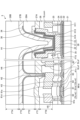

Classifications
-
- H—ELECTRICITY
- H10—SEMICONDUCTOR DEVICES; ELECTRIC SOLID-STATE DEVICES NOT OTHERWISE PROVIDED FOR
- H10K—ORGANIC ELECTRIC SOLID-STATE DEVICES
- H10K39/00—Integrated devices, or assemblies of multiple devices, comprising at least one organic radiation-sensitive element covered by group H10K30/00
- H10K39/30—Devices controlled by radiation
- H10K39/32—Organic image sensors
-
- G—PHYSICS
- G09—EDUCATION; CRYPTOGRAPHY; DISPLAY; ADVERTISING; SEALS
- G09F—DISPLAYING; ADVERTISING; SIGNS; LABELS OR NAME-PLATES; SEALS
- G09F9/00—Indicating arrangements for variable information in which the information is built-up on a support by selection or combination of individual elements
- G09F9/30—Indicating arrangements for variable information in which the information is built-up on a support by selection or combination of individual elements in which the desired character or characters are formed by combining individual elements
-
- H—ELECTRICITY
- H10—SEMICONDUCTOR DEVICES; ELECTRIC SOLID-STATE DEVICES NOT OTHERWISE PROVIDED FOR
- H10F—INORGANIC SEMICONDUCTOR DEVICES SENSITIVE TO INFRARED RADIATION, LIGHT, ELECTROMAGNETIC RADIATION OF SHORTER WAVELENGTH OR CORPUSCULAR RADIATION
- H10F30/00—Individual radiation-sensitive semiconductor devices in which radiation controls the flow of current through the devices, e.g. photodetectors
- H10F30/20—Individual radiation-sensitive semiconductor devices in which radiation controls the flow of current through the devices, e.g. photodetectors the devices having potential barriers, e.g. phototransistors
-
- H—ELECTRICITY
- H10—SEMICONDUCTOR DEVICES; ELECTRIC SOLID-STATE DEVICES NOT OTHERWISE PROVIDED FOR
- H10F—INORGANIC SEMICONDUCTOR DEVICES SENSITIVE TO INFRARED RADIATION, LIGHT, ELECTROMAGNETIC RADIATION OF SHORTER WAVELENGTH OR CORPUSCULAR RADIATION
- H10F39/00—Integrated devices, or assemblies of multiple devices, comprising at least one element covered by group H10F30/00, e.g. radiation detectors comprising photodiode arrays
- H10F39/10—Integrated devices
- H10F39/12—Image sensors
-
- G—PHYSICS
- G06—COMPUTING OR CALCULATING; COUNTING
- G06V—IMAGE OR VIDEO RECOGNITION OR UNDERSTANDING
- G06V40/00—Recognition of biometric, human-related or animal-related patterns in image or video data
- G06V40/10—Human or animal bodies, e.g. vehicle occupants or pedestrians; Body parts, e.g. hands
- G06V40/12—Fingerprints or palmprints
- G06V40/13—Sensors therefor
- G06V40/1318—Sensors therefor using electro-optical elements or layers, e.g. electroluminescent sensing
Landscapes
- Physics & Mathematics (AREA)
- General Physics & Mathematics (AREA)
- Engineering & Computer Science (AREA)
- Theoretical Computer Science (AREA)
- Solid State Image Pick-Up Elements (AREA)
- Devices For Indicating Variable Information By Combining Individual Elements (AREA)
Applications Claiming Priority (3)
| Application Number | Priority Date | Filing Date | Title |
|---|---|---|---|
| JP2021026604 | 2021-02-22 | ||
| JP2021026604 | 2021-02-22 | ||
| PCT/JP2022/002147 WO2022176503A1 (ja) | 2021-02-22 | 2022-01-21 | 検出装置 |
Publications (3)
| Publication Number | Publication Date |
|---|---|
| JPWO2022176503A1 JPWO2022176503A1 (https=) | 2022-08-25 |
| JPWO2022176503A5 JPWO2022176503A5 (https=) | 2023-09-05 |
| JP7550952B2 true JP7550952B2 (ja) | 2024-09-13 |
Family
ID=82930810
Family Applications (1)
| Application Number | Title | Priority Date | Filing Date |
|---|---|---|---|
| JP2023500655A Active JP7550952B2 (ja) | 2021-02-22 | 2022-01-21 | 検出装置 |
Country Status (3)
| Country | Link |
|---|---|
| US (1) | US20230397449A1 (https=) |
| JP (1) | JP7550952B2 (https=) |
| WO (1) | WO2022176503A1 (https=) |
Families Citing this family (1)
| Publication number | Priority date | Publication date | Assignee | Title |
|---|---|---|---|---|
| CN114597220A (zh) * | 2022-03-02 | 2022-06-07 | 武汉华星光电技术有限公司 | 指纹采集器件、显示面板 |
Citations (6)
| Publication number | Priority date | Publication date | Assignee | Title |
|---|---|---|---|---|
| JP2011014752A (ja) | 2009-07-03 | 2011-01-20 | Sony Corp | 光電変換装置および放射線撮像装置 |
| JP2013012696A (ja) | 2011-05-27 | 2013-01-17 | Sony Corp | 光電変換素子および光電変換装置 |
| JP2019169670A (ja) | 2018-03-26 | 2019-10-03 | シャープ株式会社 | アクティブマトリクス基板、及びそれを備えたx線撮像パネル |
| JP2020102555A (ja) | 2018-12-21 | 2020-07-02 | 株式会社ジャパンディスプレイ | 検出装置 |
| WO2021039161A1 (ja) | 2019-08-30 | 2021-03-04 | 株式会社ジャパンディスプレイ | 検出装置 |
| JP2021061372A (ja) | 2019-10-09 | 2021-04-15 | 株式会社ジャパンディスプレイ | 検出装置 |
Family Cites Families (6)
| Publication number | Priority date | Publication date | Assignee | Title |
|---|---|---|---|---|
| TWI292281B (en) * | 2005-12-29 | 2008-01-01 | Ind Tech Res Inst | Pixel structure of active organic light emitting diode and method of fabricating the same |
| JP2016105377A (ja) * | 2014-12-01 | 2016-06-09 | 株式会社ジャパンディスプレイ | 表示装置 |
| KR102651097B1 (ko) * | 2016-10-28 | 2024-03-22 | 엘지디스플레이 주식회사 | 발광 다이오드 디스플레이 장치 |
| KR102480089B1 (ko) * | 2017-12-01 | 2022-12-23 | 삼성디스플레이 주식회사 | 디스플레이 장치 및 그 제조방법 |
| US11856814B2 (en) * | 2019-04-12 | 2023-12-26 | HKC Corporation Limited | Display panel and manufacturing method thereof |
| CN112349232B (zh) * | 2019-08-06 | 2025-04-08 | 群创光电股份有限公司 | 显示设备及电子设备 |
-
2022
- 2022-01-21 WO PCT/JP2022/002147 patent/WO2022176503A1/ja not_active Ceased
- 2022-01-21 JP JP2023500655A patent/JP7550952B2/ja active Active
-
2023
- 2023-08-17 US US18/235,046 patent/US20230397449A1/en active Pending
Patent Citations (6)
| Publication number | Priority date | Publication date | Assignee | Title |
|---|---|---|---|---|
| JP2011014752A (ja) | 2009-07-03 | 2011-01-20 | Sony Corp | 光電変換装置および放射線撮像装置 |
| JP2013012696A (ja) | 2011-05-27 | 2013-01-17 | Sony Corp | 光電変換素子および光電変換装置 |
| JP2019169670A (ja) | 2018-03-26 | 2019-10-03 | シャープ株式会社 | アクティブマトリクス基板、及びそれを備えたx線撮像パネル |
| JP2020102555A (ja) | 2018-12-21 | 2020-07-02 | 株式会社ジャパンディスプレイ | 検出装置 |
| WO2021039161A1 (ja) | 2019-08-30 | 2021-03-04 | 株式会社ジャパンディスプレイ | 検出装置 |
| JP2021061372A (ja) | 2019-10-09 | 2021-04-15 | 株式会社ジャパンディスプレイ | 検出装置 |
Also Published As
| Publication number | Publication date |
|---|---|
| WO2022176503A1 (ja) | 2022-08-25 |
| US20230397449A1 (en) | 2023-12-07 |
| JPWO2022176503A1 (https=) | 2022-08-25 |
Similar Documents
| Publication | Publication Date | Title |
|---|---|---|
| JP7664447B2 (ja) | 検出装置 | |
| JP7642116B2 (ja) | 検出装置 | |
| JP7529455B2 (ja) | 検出装置 | |
| CN216435906U (zh) | 检测装置 | |
| US20230178674A1 (en) | Detection device, display device, and illumination device with detection function | |
| JP7550952B2 (ja) | 検出装置 | |
| CN114342079B (zh) | 检测装置 | |
| JP7496208B2 (ja) | 検出装置 | |
| US20220115424A1 (en) | Detection device | |
| JP2022029179A (ja) | 検出装置 | |
| JP7633006B2 (ja) | 検出装置 | |
| JP7518691B2 (ja) | 検出装置及び光フィルタ | |
| JP7443077B2 (ja) | 検出装置 | |
| JP7626687B2 (ja) | 検出装置 | |
| JP7598710B2 (ja) | 検出装置 |
Legal Events
| Date | Code | Title | Description |
|---|---|---|---|
| A521 | Request for written amendment filed |
Free format text: JAPANESE INTERMEDIATE CODE: A523 Effective date: 20230602 |
|
| A621 | Written request for application examination |
Free format text: JAPANESE INTERMEDIATE CODE: A621 Effective date: 20230602 |
|
| TRDD | Decision of grant or rejection written | ||
| A01 | Written decision to grant a patent or to grant a registration (utility model) |
Free format text: JAPANESE INTERMEDIATE CODE: A01 Effective date: 20240806 |
|
| A61 | First payment of annual fees (during grant procedure) |
Free format text: JAPANESE INTERMEDIATE CODE: A61 Effective date: 20240903 |
|
| R150 | Certificate of patent or registration of utility model |
Ref document number: 7550952 Country of ref document: JP Free format text: JAPANESE INTERMEDIATE CODE: R150 |
|
| S111 | Request for change of ownership or part of ownership |
Free format text: JAPANESE INTERMEDIATE CODE: R313113 |
|
| R350 | Written notification of registration of transfer |
Free format text: JAPANESE INTERMEDIATE CODE: R350 |