JP7493250B2 - 画素、固体撮像装置及び画素の製造方法 - Google Patents
画素、固体撮像装置及び画素の製造方法 Download PDFInfo
- Publication number
- JP7493250B2 JP7493250B2 JP2021533975A JP2021533975A JP7493250B2 JP 7493250 B2 JP7493250 B2 JP 7493250B2 JP 2021533975 A JP2021533975 A JP 2021533975A JP 2021533975 A JP2021533975 A JP 2021533975A JP 7493250 B2 JP7493250 B2 JP 7493250B2
- Authority
- JP
- Japan
- Prior art keywords
- light
- region
- pixel
- conversion unit
- photoelectric conversion
- Prior art date
- Legal status (The legal status is an assumption and is not a legal conclusion. Google has not performed a legal analysis and makes no representation as to the accuracy of the status listed.)
- Active
Links
Images

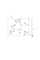


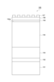


Classifications
-
- H—ELECTRICITY
- H04—ELECTRIC COMMUNICATION TECHNIQUE
- H04N—PICTORIAL COMMUNICATION, e.g. TELEVISION
- H04N23/00—Cameras or camera modules comprising electronic image sensors; Control thereof
- H04N23/20—Cameras or camera modules comprising electronic image sensors; Control thereof for generating image signals from infrared radiation only
- H04N23/21—Cameras or camera modules comprising electronic image sensors; Control thereof for generating image signals from infrared radiation only from near infrared [NIR] radiation
-
- H—ELECTRICITY
- H04—ELECTRIC COMMUNICATION TECHNIQUE
- H04N—PICTORIAL COMMUNICATION, e.g. TELEVISION
- H04N25/00—Circuitry of solid-state image sensors [SSIS]; Control thereof
- H04N25/70—SSIS architectures; Circuits associated therewith
-
- H—ELECTRICITY
- H10—SEMICONDUCTOR DEVICES; ELECTRIC SOLID-STATE DEVICES NOT OTHERWISE PROVIDED FOR
- H10F—INORGANIC SEMICONDUCTOR DEVICES SENSITIVE TO INFRARED RADIATION, LIGHT, ELECTROMAGNETIC RADIATION OF SHORTER WAVELENGTH OR CORPUSCULAR RADIATION
- H10F30/00—Individual radiation-sensitive semiconductor devices in which radiation controls the flow of current through the devices, e.g. photodetectors
- H10F30/20—Individual radiation-sensitive semiconductor devices in which radiation controls the flow of current through the devices, e.g. photodetectors the devices having potential barriers, e.g. phototransistors
-
- H—ELECTRICITY
- H10—SEMICONDUCTOR DEVICES; ELECTRIC SOLID-STATE DEVICES NOT OTHERWISE PROVIDED FOR
- H10F—INORGANIC SEMICONDUCTOR DEVICES SENSITIVE TO INFRARED RADIATION, LIGHT, ELECTROMAGNETIC RADIATION OF SHORTER WAVELENGTH OR CORPUSCULAR RADIATION
- H10F39/00—Integrated devices, or assemblies of multiple devices, comprising at least one element covered by group H10F30/00, e.g. radiation detectors comprising photodiode arrays
- H10F39/10—Integrated devices
-
- H—ELECTRICITY
- H10—SEMICONDUCTOR DEVICES; ELECTRIC SOLID-STATE DEVICES NOT OTHERWISE PROVIDED FOR
- H10F—INORGANIC SEMICONDUCTOR DEVICES SENSITIVE TO INFRARED RADIATION, LIGHT, ELECTROMAGNETIC RADIATION OF SHORTER WAVELENGTH OR CORPUSCULAR RADIATION
- H10F39/00—Integrated devices, or assemblies of multiple devices, comprising at least one element covered by group H10F30/00, e.g. radiation detectors comprising photodiode arrays
- H10F39/10—Integrated devices
- H10F39/12—Image sensors
-
- H—ELECTRICITY
- H10—SEMICONDUCTOR DEVICES; ELECTRIC SOLID-STATE DEVICES NOT OTHERWISE PROVIDED FOR
- H10F—INORGANIC SEMICONDUCTOR DEVICES SENSITIVE TO INFRARED RADIATION, LIGHT, ELECTROMAGNETIC RADIATION OF SHORTER WAVELENGTH OR CORPUSCULAR RADIATION
- H10F77/00—Constructional details of devices covered by this subclass
- H10F77/40—Optical elements or arrangements
Landscapes
- Engineering & Computer Science (AREA)
- Multimedia (AREA)
- Signal Processing (AREA)
- Health & Medical Sciences (AREA)
- Toxicology (AREA)
- Solid State Image Pick-Up Elements (AREA)
- Light Receiving Elements (AREA)
- Transforming Light Signals Into Electric Signals (AREA)
Applications Claiming Priority (5)
| Application Number | Priority Date | Filing Date | Title |
|---|---|---|---|
| JP2019134322 | 2019-07-22 | ||
| JP2019134322 | 2019-07-22 | ||
| JP2020018082 | 2020-02-05 | ||
| JP2020018082 | 2020-02-05 | ||
| PCT/JP2020/027504 WO2021015070A1 (ja) | 2019-07-22 | 2020-07-15 | 画素、固体撮像装置及び画素の製造方法 |
Publications (2)
| Publication Number | Publication Date |
|---|---|
| JPWO2021015070A1 JPWO2021015070A1 (https=) | 2021-01-28 |
| JP7493250B2 true JP7493250B2 (ja) | 2024-05-31 |
Family
ID=74193473
Family Applications (1)
| Application Number | Title | Priority Date | Filing Date |
|---|---|---|---|
| JP2021533975A Active JP7493250B2 (ja) | 2019-07-22 | 2020-07-15 | 画素、固体撮像装置及び画素の製造方法 |
Country Status (2)
| Country | Link |
|---|---|
| JP (1) | JP7493250B2 (https=) |
| WO (1) | WO2021015070A1 (https=) |
Citations (4)
| Publication number | Priority date | Publication date | Assignee | Title |
|---|---|---|---|---|
| JP2006509358A (ja) | 2002-12-09 | 2006-03-16 | クォンタム セミコンダクター リミテッド ライアビリティ カンパニー | Cmos画像センサー |
| JP2010263158A (ja) | 2009-05-11 | 2010-11-18 | Sony Corp | 2次元固体撮像装置、及び、2次元固体撮像装置における偏光光データ処理方法 |
| JP2015232599A (ja) | 2014-06-09 | 2015-12-24 | ソニー株式会社 | 光学フィルタ、固体撮像装置、および電子機器 |
| WO2016136502A1 (ja) | 2015-02-26 | 2016-09-01 | ソニー株式会社 | 固体撮像素子、および電子装置 |
Family Cites Families (1)
| Publication number | Priority date | Publication date | Assignee | Title |
|---|---|---|---|---|
| JP2012064703A (ja) * | 2010-09-15 | 2012-03-29 | Sony Corp | 撮像素子および撮像装置 |
-
2020
- 2020-07-15 JP JP2021533975A patent/JP7493250B2/ja active Active
- 2020-07-15 WO PCT/JP2020/027504 patent/WO2021015070A1/ja not_active Ceased
Patent Citations (4)
| Publication number | Priority date | Publication date | Assignee | Title |
|---|---|---|---|---|
| JP2006509358A (ja) | 2002-12-09 | 2006-03-16 | クォンタム セミコンダクター リミテッド ライアビリティ カンパニー | Cmos画像センサー |
| JP2010263158A (ja) | 2009-05-11 | 2010-11-18 | Sony Corp | 2次元固体撮像装置、及び、2次元固体撮像装置における偏光光データ処理方法 |
| JP2015232599A (ja) | 2014-06-09 | 2015-12-24 | ソニー株式会社 | 光学フィルタ、固体撮像装置、および電子機器 |
| WO2016136502A1 (ja) | 2015-02-26 | 2016-09-01 | ソニー株式会社 | 固体撮像素子、および電子装置 |
Also Published As
| Publication number | Publication date |
|---|---|
| WO2021015070A1 (ja) | 2021-01-28 |
| JPWO2021015070A1 (https=) | 2021-01-28 |
Similar Documents
| Publication | Publication Date | Title |
|---|---|---|
| US12557402B2 (en) | Shallow trench textured regions and associated methods | |
| US8269299B2 (en) | Two-dimensional solid-state imaging device | |
| TWI298947B (en) | Solid-state imaging device and method for manufacturing the same | |
| CN108257985A (zh) | 光传感器 | |
| TWI841659B (zh) | 用於檢測不同波長的光檢測裝置 | |
| TW201101474A (en) | Multilayer image sensor pixel structure for reducing crosstalk | |
| US20150097157A1 (en) | Infrared solid-state imaging device | |
| US11258971B2 (en) | Multi-function transfer gate electrode for a photodetector and methods of operating the same | |
| TW202127647A (zh) | 具有分離像素結構之影像感測器及其製造方法 | |
| JP2012151452A (ja) | 裏面に設けられた金属テクスチャリングによって最適化された光検出器 | |
| TW201218364A (en) | Solid imaging device | |
| EP3794643B1 (en) | Integration of a short-wave infrared detector with cmos compatible substrates | |
| JP7493250B2 (ja) | 画素、固体撮像装置及び画素の製造方法 | |
| US20200357833A1 (en) | Short-wave infrared detector array and fabrication methods thereof | |
| CN117178367A (zh) | 宽带图像装置及其制造方法 | |
| TWI886545B (zh) | 影像感測裝置及其形成方法 | |
| CN116724401A (zh) | 固体拍摄装置以及固体拍摄装置的制造方法 |
Legal Events
| Date | Code | Title | Description |
|---|---|---|---|
| A621 | Written request for application examination |
Free format text: JAPANESE INTERMEDIATE CODE: A621 Effective date: 20230613 |
|
| TRDD | Decision of grant or rejection written | ||
| A01 | Written decision to grant a patent or to grant a registration (utility model) |
Free format text: JAPANESE INTERMEDIATE CODE: A01 Effective date: 20240507 |
|
| A61 | First payment of annual fees (during grant procedure) |
Free format text: JAPANESE INTERMEDIATE CODE: A61 Effective date: 20240514 |
|
| R150 | Certificate of patent or registration of utility model |
Ref document number: 7493250 Country of ref document: JP Free format text: JAPANESE INTERMEDIATE CODE: R150 |