EP3794643B1 - Integration of a short-wave infrared detector with cmos compatible substrates - Google Patents
Integration of a short-wave infrared detector with cmos compatible substrates Download PDFInfo
- Publication number
- EP3794643B1 EP3794643B1 EP18726412.2A EP18726412A EP3794643B1 EP 3794643 B1 EP3794643 B1 EP 3794643B1 EP 18726412 A EP18726412 A EP 18726412A EP 3794643 B1 EP3794643 B1 EP 3794643B1
- Authority
- EP
- European Patent Office
- Prior art keywords
- layer
- buffer layer
- slightly doped
- doped buffer
- readout
- Prior art date
- Legal status (The legal status is an assumption and is not a legal conclusion. Google has not performed a legal analysis and makes no representation as to the accuracy of the status listed.)
- Active
Links
- 239000000758 substrate Substances 0.000 title description 20
- 230000010354 integration Effects 0.000 title description 3
- 238000000034 method Methods 0.000 claims description 64
- 238000010521 absorption reaction Methods 0.000 claims description 61
- 238000000151 deposition Methods 0.000 claims description 25
- 230000008021 deposition Effects 0.000 claims description 22
- 238000000137 annealing Methods 0.000 claims description 15
- 238000004519 manufacturing process Methods 0.000 claims description 14
- 238000005516 engineering process Methods 0.000 claims description 11
- 229910052710 silicon Inorganic materials 0.000 claims description 8
- 238000012546 transfer Methods 0.000 claims description 8
- XUIMIQQOPSSXEZ-UHFFFAOYSA-N Silicon Chemical compound [Si] XUIMIQQOPSSXEZ-UHFFFAOYSA-N 0.000 claims description 7
- 229910052732 germanium Inorganic materials 0.000 claims description 7
- 239000010703 silicon Substances 0.000 claims description 7
- 230000000694 effects Effects 0.000 claims description 4
- 229910052718 tin Inorganic materials 0.000 claims description 4
- 230000031700 light absorption Effects 0.000 claims description 3
- 238000007517 polishing process Methods 0.000 claims description 3
- 235000012431 wafers Nutrition 0.000 description 32
- 239000000463 material Substances 0.000 description 28
- 239000000835 fiber Substances 0.000 description 19
- 238000001514 detection method Methods 0.000 description 15
- 238000003384 imaging method Methods 0.000 description 15
- 239000006096 absorbing agent Substances 0.000 description 13
- 238000003491 array Methods 0.000 description 13
- 229910045601 alloy Inorganic materials 0.000 description 11
- 239000000956 alloy Substances 0.000 description 11
- 230000005684 electric field Effects 0.000 description 10
- 230000003287 optical effect Effects 0.000 description 9
- VYPSYNLAJGMNEJ-UHFFFAOYSA-N Silicium dioxide Chemical compound O=[Si]=O VYPSYNLAJGMNEJ-UHFFFAOYSA-N 0.000 description 7
- PNEYBMLMFCGWSK-UHFFFAOYSA-N aluminium oxide Inorganic materials [O-2].[O-2].[O-2].[Al+3].[Al+3] PNEYBMLMFCGWSK-UHFFFAOYSA-N 0.000 description 7
- 238000006243 chemical reaction Methods 0.000 description 7
- 229910052593 corundum Inorganic materials 0.000 description 7
- 229910052814 silicon oxide Inorganic materials 0.000 description 7
- 229910001845 yogo sapphire Inorganic materials 0.000 description 7
- 239000013307 optical fiber Substances 0.000 description 6
- 229910001218 Gallium arsenide Inorganic materials 0.000 description 5
- 238000001228 spectrum Methods 0.000 description 4
- 229910000530 Gallium indium arsenide Inorganic materials 0.000 description 3
- 229910004541 SiN Inorganic materials 0.000 description 3
- KXNLCSXBJCPWGL-UHFFFAOYSA-N [Ga].[As].[In] Chemical compound [Ga].[As].[In] KXNLCSXBJCPWGL-UHFFFAOYSA-N 0.000 description 3
- 238000004458 analytical method Methods 0.000 description 3
- 238000009826 distribution Methods 0.000 description 3
- 230000005670 electromagnetic radiation Effects 0.000 description 3
- 238000012634 optical imaging Methods 0.000 description 3
- 239000004065 semiconductor Substances 0.000 description 3
- 238000004611 spectroscopical analysis Methods 0.000 description 3
- 239000010409 thin film Substances 0.000 description 3
- 230000008901 benefit Effects 0.000 description 2
- 238000000701 chemical imaging Methods 0.000 description 2
- 239000013078 crystal Substances 0.000 description 2
- 238000002513 implantation Methods 0.000 description 2
- 229910052500 inorganic mineral Inorganic materials 0.000 description 2
- 239000011707 mineral Substances 0.000 description 2
- 239000000203 mixture Substances 0.000 description 2
- 238000012545 processing Methods 0.000 description 2
- 230000002441 reversible effect Effects 0.000 description 2
- 230000035945 sensitivity Effects 0.000 description 2
- BVKZGUZCCUSVTD-UHFFFAOYSA-L Carbonate Chemical compound [O-]C([O-])=O BVKZGUZCCUSVTD-UHFFFAOYSA-L 0.000 description 1
- 229910005898 GeSn Inorganic materials 0.000 description 1
- 230000015556 catabolic process Effects 0.000 description 1
- 239000011248 coating agent Substances 0.000 description 1
- 238000000576 coating method Methods 0.000 description 1
- 230000000295 complement effect Effects 0.000 description 1
- 238000010276 construction Methods 0.000 description 1
- 230000001808 coupling effect Effects 0.000 description 1
- 238000010168 coupling process Methods 0.000 description 1
- 238000005859 coupling reaction Methods 0.000 description 1
- 238000006880 cross-coupling reaction Methods 0.000 description 1
- 238000005137 deposition process Methods 0.000 description 1
- 238000000605 extraction Methods 0.000 description 1
- 239000002803 fossil fuel Substances 0.000 description 1
- 230000004927 fusion Effects 0.000 description 1
- GNPVGFCGXDBREM-UHFFFAOYSA-N germanium atom Chemical compound [Ge] GNPVGFCGXDBREM-UHFFFAOYSA-N 0.000 description 1
- 239000003292 glue Substances 0.000 description 1
- 229910052739 hydrogen Inorganic materials 0.000 description 1
- 239000001257 hydrogen Substances 0.000 description 1
- -1 hydrogen ions Chemical class 0.000 description 1
- 125000002887 hydroxy group Chemical group [H]O* 0.000 description 1
- 230000003116 impacting effect Effects 0.000 description 1
- 239000012212 insulator Substances 0.000 description 1
- 238000011835 investigation Methods 0.000 description 1
- 230000005865 ionizing radiation Effects 0.000 description 1
- 238000013507 mapping Methods 0.000 description 1
- 238000005259 measurement Methods 0.000 description 1
- 229910044991 metal oxide Inorganic materials 0.000 description 1
- 150000004706 metal oxides Chemical class 0.000 description 1
- 238000001465 metallisation Methods 0.000 description 1
- MYWUZJCMWCOHBA-VIFPVBQESA-N methamphetamine Chemical compound CN[C@@H](C)CC1=CC=CC=C1 MYWUZJCMWCOHBA-VIFPVBQESA-N 0.000 description 1
- 238000012544 monitoring process Methods 0.000 description 1
- 238000012014 optical coherence tomography Methods 0.000 description 1
- 230000002085 persistent effect Effects 0.000 description 1
- 238000010791 quenching Methods 0.000 description 1
- 230000000171 quenching effect Effects 0.000 description 1
- 238000007493 shaping process Methods 0.000 description 1
- 230000003595 spectral effect Effects 0.000 description 1
- 239000000126 substance Substances 0.000 description 1
- 150000003467 sulfuric acid derivatives Chemical class 0.000 description 1
- 230000002123 temporal effect Effects 0.000 description 1
- 239000012780 transparent material Substances 0.000 description 1
Images


Classifications
-
- H—ELECTRICITY
- H01—ELECTRIC ELEMENTS
- H01L—SEMICONDUCTOR DEVICES NOT COVERED BY CLASS H10
- H01L27/00—Devices consisting of a plurality of semiconductor or other solid-state components formed in or on a common substrate
- H01L27/14—Devices consisting of a plurality of semiconductor or other solid-state components formed in or on a common substrate including semiconductor components sensitive to infrared radiation, light, electromagnetic radiation of shorter wavelength or corpuscular radiation and specially adapted either for the conversion of the energy of such radiation into electrical energy or for the control of electrical energy by such radiation
- H01L27/144—Devices controlled by radiation
- H01L27/146—Imager structures
- H01L27/14601—Structural or functional details thereof
- H01L27/14632—Wafer-level processed structures
-
- H—ELECTRICITY
- H01—ELECTRIC ELEMENTS
- H01L—SEMICONDUCTOR DEVICES NOT COVERED BY CLASS H10
- H01L27/00—Devices consisting of a plurality of semiconductor or other solid-state components formed in or on a common substrate
- H01L27/14—Devices consisting of a plurality of semiconductor or other solid-state components formed in or on a common substrate including semiconductor components sensitive to infrared radiation, light, electromagnetic radiation of shorter wavelength or corpuscular radiation and specially adapted either for the conversion of the energy of such radiation into electrical energy or for the control of electrical energy by such radiation
- H01L27/144—Devices controlled by radiation
- H01L27/146—Imager structures
- H01L27/14643—Photodiode arrays; MOS imagers
- H01L27/14649—Infrared imagers
-
- H—ELECTRICITY
- H01—ELECTRIC ELEMENTS
- H01L—SEMICONDUCTOR DEVICES NOT COVERED BY CLASS H10
- H01L27/00—Devices consisting of a plurality of semiconductor or other solid-state components formed in or on a common substrate
- H01L27/14—Devices consisting of a plurality of semiconductor or other solid-state components formed in or on a common substrate including semiconductor components sensitive to infrared radiation, light, electromagnetic radiation of shorter wavelength or corpuscular radiation and specially adapted either for the conversion of the energy of such radiation into electrical energy or for the control of electrical energy by such radiation
- H01L27/144—Devices controlled by radiation
- H01L27/146—Imager structures
- H01L27/14665—Imagers using a photoconductor layer
- H01L27/14669—Infrared imagers
-
- H—ELECTRICITY
- H01—ELECTRIC ELEMENTS
- H01L—SEMICONDUCTOR DEVICES NOT COVERED BY CLASS H10
- H01L27/00—Devices consisting of a plurality of semiconductor or other solid-state components formed in or on a common substrate
- H01L27/14—Devices consisting of a plurality of semiconductor or other solid-state components formed in or on a common substrate including semiconductor components sensitive to infrared radiation, light, electromagnetic radiation of shorter wavelength or corpuscular radiation and specially adapted either for the conversion of the energy of such radiation into electrical energy or for the control of electrical energy by such radiation
- H01L27/144—Devices controlled by radiation
- H01L27/146—Imager structures
- H01L27/14683—Processes or apparatus peculiar to the manufacture or treatment of these devices or parts thereof
- H01L27/14687—Wafer level processing
-
- H—ELECTRICITY
- H01—ELECTRIC ELEMENTS
- H01L—SEMICONDUCTOR DEVICES NOT COVERED BY CLASS H10
- H01L27/00—Devices consisting of a plurality of semiconductor or other solid-state components formed in or on a common substrate
- H01L27/14—Devices consisting of a plurality of semiconductor or other solid-state components formed in or on a common substrate including semiconductor components sensitive to infrared radiation, light, electromagnetic radiation of shorter wavelength or corpuscular radiation and specially adapted either for the conversion of the energy of such radiation into electrical energy or for the control of electrical energy by such radiation
- H01L27/144—Devices controlled by radiation
- H01L27/146—Imager structures
- H01L27/14683—Processes or apparatus peculiar to the manufacture or treatment of these devices or parts thereof
- H01L27/1469—Assemblies, i.e. hybrid integration
-
- H—ELECTRICITY
- H04—ELECTRIC COMMUNICATION TECHNIQUE
- H04N—PICTORIAL COMMUNICATION, e.g. TELEVISION
- H04N23/00—Cameras or camera modules comprising electronic image sensors; Control thereof
- H04N23/20—Cameras or camera modules comprising electronic image sensors; Control thereof for generating image signals from infrared radiation only
- H04N23/23—Cameras or camera modules comprising electronic image sensors; Control thereof for generating image signals from infrared radiation only from thermal infrared radiation
-
- H—ELECTRICITY
- H04—ELECTRIC COMMUNICATION TECHNIQUE
- H04N—PICTORIAL COMMUNICATION, e.g. TELEVISION
- H04N5/00—Details of television systems
- H04N5/30—Transforming light or analogous information into electric information
- H04N5/33—Transforming infrared radiation
Definitions
- the invention relates to the manufacturing of electromagnetic radiation detector arrays for intensity detection and imaging comprising Complementary Metal Oxide Semiconductor (CMOS) circuits and absorption materials, both sensitive to high temperature. More precisely the invention relates to short-wave infrared (SWIR) detector arrays, to optical systems comprising such arrays and to methods for forming such detector arrays and also to applications thereof.
- CMOS Complementary Metal Oxide Semiconductor
- SWIR short-wave infrared
- Intensity and imaging detectors equally named electromagnetic radiation photodiodes respectively Focal Plane Arrays (FPAs), are designed to convert the optical generation of electron-hole pairs released by impacting photons into electrical signals, further processed by a readout electronics and represented as an image on a computer screen.
- FPAs Focal Plane Arrays
- these detectors also offer spectral resolution, since the energy of each incident photon is proportional to the number of generated electron-hole pairs and thus measurable by pulse height analysis.
- Intensity detector arrays and FPAs employing direct conversion by means of semiconductor absorbers, can currently be implemented in different ways. They can first be achieved by various material depositions. Polycrystalline or amorphous materials may directly be deposited on the readout electronics made from thin film transistors, whereas single crystals - that have better transport properties - could eventually be epitaxial grown on CMOS processed readout wafers, provided specific metallization schemes will allow for high process temperatures. To the current state of knowledge, this option could't be realized so far.
- intensity detector arrays FPAs may be integrated by various bonding processes.
- the absorber is bonded by bump-bonding that allows for the use of any suitable semiconductor material from which large crystals may be grown, such as Si, Ge or GaAs. While with this technique it is a great challenge to push the pixel size below 50 ⁇ m, bump bonding is replaced by fusion bonding, including bonding with a patterned surface such as semiconducting pads surrounded by oxide. Both ways lead to complex structures that prevent a widespread use of the technology.
- the absorber layer and the CMOS layer are monolithically integrated by covalent bonding and subsequent annealing steps. Whereas the pixel size may be reduced by this method, according to our information, an efficient electrically conductive photodiode structure could't be demonstrated till now.
- intensity detector arrays and FPAs may be achieved by different absorber materials that are either application or integration specific, depending on their sensitivity, absorption or manufacturability, among others.
- Si-based detectors can eventually be manufactured without the use of a bonding process as a high-resistivity absorber layer may be epitaxially grown directly on the CMOS Si substrate. The readout electronics is then CMOS processed in this epitaxial layer and the substrate subsequently removed [Mattiazzo, 2013]. While these detectors may be used for ionizing radiation in high-energy physics, detection in the short-wave infrared (SWIR) spectrum is not possible with Si-based absorbers.
- SWIR short-wave infrared
- Wavelengths detection between 1.00 and 1.55 ⁇ m usually requires indium-gallium-arsenide (InGaAs) absorption materials, whereas recent studies have demonstrated that GeSn-type alloys are better candidates with a higher cutoff wavelength and a better sensitivity.
- InGaAs indium-gallium-arsenide
- GeSn-type alloys are better candidates with a higher cutoff wavelength and a better sensitivity.
- the GeSn growth process itself can be performed at low temperature - between 300°C and 330°C - its direct growth on Si is not reliable enough because of lattices mismatch and difference in the dilatation coefficients so that the integration process requires a buffer layer.
- this can only be obtained at high annealing temperatures.
- the invention relates to a method of fabricating an intensity detector array, in particular a short-wave infrared focal plane array (SWIR FPA), comprising a temperature sensitive conversion layer temperature sensitive a CMOS wafer, and a p-n junction in order to allow for an efficient charge collection between both layers.
- SWIR FPA short-wave infrared focal plane array
- the detector array has basically a p-i-n diode structure, further described as an avalanche photodiode (APD) structure including a lightly p-doped i-region.
- APD avalanche photodiode
- the SWIR detector array is realized by a method of fabrication comprising the deposition of a buffer layer onto the CMOS processed wafer and applying energy onto it, comprising the step of using annealing at very short light pulses duration, before providing the conversion layer on top of the buffer layer.
- FPA focal plane array
- the invention is achieved by a method of fabrication of a short-wave infrared detector array comprising a silicon readout wafer having a deposition surface and comprising a CMOS readout layer.
- the short-wave infrared detector array comprises a slightly doped buffer layer situated on said deposition surface and comprises a short-wave infrared light absorption layer, comprising Ge and Sn, situated on said doped buffer layer.
- the method of the invention comprises the steps (A-D) of:
- said absorption layer consists in a Ge 1-x Sn x alloy.
- said absorption layer has a Sn content x between 0.05 ⁇ x ⁇ 0.25.
- said absorption layer consists in a Si x Ge 1-x-z Sn z alloy.
- said absorption layer has a Si content x between 0 ⁇ x ⁇ 0.2.
- said absorption layer has a Sn content z between 0.05 ⁇ z ⁇ 0.15.
- said absorption layer comprises an i-type Ge 1-x Sn x layer, in contact with said slightly doped buffer layer.
- said i-type Ge 1-x Sn x layer has a thickness between 250nm and 5 ⁇ m, preferably between 250 ⁇ m and 3 ⁇ m.
- said absorption layer comprises, between said slightly doped buffer layer and said i-type Ge 1-x Sn x layer, a p+-type doped Ge 1-x Sn x layer having a doping concentration between 10 19 to 5 ⁇ 10 20 cm -3 .
- said absorption layer comprises an i-type Si x Ge 1-x-z Sn z layer, in contact with said slightly doped buffer layer.
- the thickness of said absorption layer in all the embodiments of the invention is between 2 nm and 5 ⁇ m.
- the absorption layer is realized by an epitaxial lift-off process.
- said slightly doped buffer layer is a p-type doped Ge layer having a doping concentration between 10 14 to 10 15 cm -3 .
- said slightly doped buffer layer is realized by a technology including wafer-bonding and a layer splitting process.
- said slightly doped buffer layer is realized by an epitaxial lift-off transfer process.
- said slightly buffer layer is a p-type doped Ge 1-x Sn x layer having a doping concentration between 10 14 to 10 15 cm -3 .
- said p-type doped Ge 1-x Sn x buffer layer is realized by a technology including wafer-bonding and a layer splitting process.
- said buffer layer is realized by a technology including wafer-bonding and an etch back and/or polishing process.
- said slightly doped buffer layer is realized by an epitaxial lift-off transfer process.
- the thickness of said slightly doped buffer layer in all the embodiments of the invention is between 5 nm and 3 ⁇ m.
- said slightly doped buffer layer is etched after step B or after step C so as to provide an etched area of said slightly doped buffer layer.
- said slightly doped buffer layer is at least partially covered after step B or after step C so as to provide a selectively covered area of said slightly doped buffer layer.
- said etched area is covered by materials selected from: SiO x , SiN, Al 2 O 3 .
- said selectively covered area is covered by materials selected from: SiO x , SiN, Al 2 O 3 .
- the annealing temperature of said interface layer during the annealing process step C is higher than 650°C and lower than 750°C.
- said light source provides light having a wavelength that is comprised between 300 nm and 900 nm.
- the light is provided by a pulsed light source providing light pulses having a pulse duration of said light pulses lower than 1 ms, preferably lower than 100 ns.
- the light source comprises at least one laser.
- the light source comprises at least one pulsed lamp.
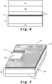
- Fig. 1 illustrates a SWIR detector array 1 of prior art.
- a detector array comprises typically a microlens array (A) and an absorber sheet typically made of InGaAs (B), as well as a readout circuit realized on a separate layer or wafer.
- the stack comprising the optical layer (A) and the absorber layer (B) is electrically and mechanically connected to the CMOS layer (C) by an array of bumps (D).
- the device of the invention provides a highly efficient monolithic SWIR detector array 1 comprising a simplified 3D integrated structure having a small thickness, a reduced weight and lower power requirements.
- the SWIR detector array 1 of the invention is also called a focal plane array (FPA) hereafter.
- FPA focal plane array
- the device of the invention allows to provide very sensitive and large area monolithic FPAs able to cover efficiently the whole SWIR spectrum at room-temperature or eventually Peltier-cooled operation.
- Said SWIR spectrum is defined by a wavelengths range between 1.0 ⁇ m and 3.0 ⁇ m.
- the SWIR detector array 1 of the invention illustrated in Fig. 3 , comprises at least:
- the SWIR detector array 1 of the invention may be configured to be suited for intensity measurements or as an imaging array in which case the detector array is called a Focal Plane Array as it is intended to be placed in the focal plane of an optical system.
- the SWIR detector array 1 comprises also an electrical contact layer 50 and a back contact configured to apply an electrical potential across the layers of the detector array 1.
- the electrical contact layer 50 may be a metallic layer, a transparent conducting layer or may be a doped layer such as a highly p or n-doped layer.
- said readout wafer 20 is a p-doped or n-doped wafer, but not necessarily so.
- the readout wafer of the detector 1 of the invention may be configured in different ways but comprises always at least one electrical charge collecting area.
- the readout wafer comprises an array of electrical charge collecting structures.
- the electrical charge collecting structures are preferably doped regions.
- the array of electrical charge collecting structures may be a 2D array, for example an array comprising 50 x 50 electrical charge collecting areas.
- the array of charge collectors array may be a 1D array, comprising at least two charge collecting areas, which can be particularly useful in intensity detection applications comprising waveguides as described further.
- the, 1D or 2D SWIR detector array 1 may be made of an assembly of SWIR detectors 1 of the invention, comprising each a low number of electrical charge collecting areas, for example 10 electrical charge collecting areas per detector array 1.
- the detector array 1 may comprise widely spaced charge collecting areas.
- the detector array 1 is a FPA comprising densely packed charge collecting areas, as illustrated in Fig. 5 illustrating a single pixel of a FPA.
- Fig. 4 illustrates the electrical field across an embodiment of the SWIR detector array 1 in operation.
- the electrical potential drop across the detector array 1 produces an electrical field E, illustrated in the graph of Fig. 4.
- Fig. 4 illustrates also an avalanche region (AV) provided by an electrical field E applied across the detector array 1.
- AV avalanche region
- the readout electronics is preferably processed in an epitaxial Si layer with a thickness of about 10 - 30 ⁇ m and a resistivity above about 500 Qcm or preferably about 1 - 2 k ⁇ cm or more preferably 2 - 5 k ⁇ 2cm or even above 5 k ⁇ cm, for example 5 - 50 k ⁇ cm, the resistivity being due to a low doping level in between about 10 11 to 10 13 cm -3 of a first conduction type (for example n-conduction induced by n-doping).
- silicon-on-insulator (SOI) wafers may be used for the CMOS processing of the readout electronics.
- SOI silicon-on-insulator
- a silicon layer 20 may comprise n+ charge collectors 24.
- said absorption layer 40 is a lightly p-doped layer. In operation, each photon incident on the absorption layer 40 creates an electron-hole pair in the absorber 40. The hole is collected at the incident light side and the electron, created by the absorption of a photon, drifts to the avalanche region AV ( Fig.
- the SWIR detector array 1 such as a FPA of the invention provides single-photon detection. It is therefore suitable for energy discrimination, whereby the energy of photons incident on the absorber can be measured by employing the pulse height analysis of the electrical pulses processed by the readout electronics.
- said buffer layer 30 consists of a slightly doped Ge layer and is preferably a p-type doped Ge layer having a doping concentration between 10 14 to 10 15 cm -3 .
- said slightly doped buffer layer 30 is made of Ge 1-x Sn x and has a Sn content x between 0.00 ⁇ x ⁇ 0.03, and is preferably a p-type doped Ge 1-x Sn x layer having a doping concentration between 10 14 to 10 15 cm -3 .
- said slightly doped buffer layer 30 may be advantageously be realized by an epitaxial lift-off transfer process.
- said buffer layer (30 is realized by a technology including wafer-bonding and an etch back and/or a polishing process.
- said absorption layer 40 consists in a Ge 1-x Sn x alloy.
- Said absorption layer 40 has preferably a Sn content x between 0.05 ⁇ x ⁇ 0.25.
- said absorption layer 40 consists in a Si x Ge 1-x-z Sn z alloy and has preferably a Si content x between 0 ⁇ x ⁇ 0.2.
- the absorption layer 40 consisting in a Si x Ge 1-x-z Sn z alloy said absorption layer 40 has a Sn content z between 0.05 ⁇ z ⁇ 0.15.
- said absorption layer 40 comprises an i-type Ge 1-x Sn x layer 42 being in contact with said slightly doped buffer layer 30. This layer can absorb up to 100% of the incident light with a photon wavelength greater than 1.4 ⁇ m, depending on the thickness.
- Said i-type Ge 1-x Sn x layer may have a thickness between 250 nm and 5 ⁇ m, preferably between 250 nm and 3 ⁇ m.
- said absorption layer 40 comprises, between said slightly doped buffer layer 30 and said i-type Ge 1-x Sn x layer 42, a p + -type doped Ge 1-x Sn x layer 44 having a doping concentration between 10 19 to 5 ⁇ 10 20 cm -3 .
- said absorption layer 40 comprises an i-type Si x Ge 1-x-z Sn z layer, in contact with said slightly doped buffer layer 30.
- said absorption layer 40 comprises, between said slightly doped buffer layer 30 and said i-type Si x Ge 1-x-z Sn z layer, a p+-type doped Ge 1-x Sn x layer having a doping concentration between 10 19 to 5x1020 cm -3 .
- the thickness of the absorption layer 40 is between 2 nm and 5 ⁇ m. In a variant, the thickness of the absorption layer 40 is between 1nm and 1000 ⁇ m.
- an etched area 34 may be provided in the buffer layer 30.
- This etched area 34 extends across the whole thickness of the buffer layer 30 and may serve to deposit other materials, different to the buffer material, directly on said deposition surface 20a. These added other materials my serve to avoid the growth of absorption alloys such as Ge 1-x Sn x and Si x Ge 1-x-z Sn z over predetermined areas.
- said etched area 34 may be covered by materials selected from: SiO x wherein 1.9 ⁇ x ⁇ 2.0, SiN, HfO, Al 2 O 3 . Said coverage is not limited to these materials.
- a portion of the buffer layer 30 may also comprise a selectively covered area that is covered by materials selected from: SiO x wherein 1.9 ⁇ x ⁇ 2.0, SiN, HfO, Al 2 O 3 . These added other materials my serve to avoid the growth of absorption alloys such as Ge 1-x Sn x and Si x Ge 1-x-z Sn z on the whole extension of the buffer layer.
- At least a portion of said etched area 34 and a portion of said buffer layer 30 may be covered by materials selected from: SiO x wherein 1.9 ⁇ x ⁇ 2.0, SiN, HfO, Al 2 O 3 .
- said etched area 34 and a portion of said buffer layer 30 are covered by different materials.
- an optical layer having optical focusing properties may be arranged between said absorption layer 40 and said buffer layer.
- at least one side of said absorption layer 30 may be corrugated and have for example the shape of an array of microlenses so as to provide a focused light beam on a focal plane coincident with said interfacial layer 32.
- the interface layer 32 will have the same structured or corrugated shape as the structured or corrugated surface of said absorption layer 30.
- an antireflection coating is added in order to maximize the amount of light coupled into the device/absorbing layer.
- composition and thickness of any of the layers of the detector 1 may be configured so as to shape a predetermined electrical field profile across the avalanche region (AV) of the detector 1. Shaping electrical field profiles is well known in the art and is not further commented here.
- FIG. 5 An exemplary execution of a small part of the cross-section of the thinned CMOS processed readout wafer 20 of a SWIR detector array 1 comprises a p-n junction 22 is now described and illustrated in Fig. 5 .
- the width of the section illustrated in figure 5 defined in the plane of the readout wafer 21, corresponds to slightly more than a single pixel size of the detector array 1, and may range for example from 5 -20 ⁇ m,20 - 50 ⁇ m,50 -100 ⁇ m, depending on the CMOS process used.
- n-wells 25 serve as charge collectors, collecting electrons coming from electron-hole pairs which are generated by incident photons and separated in the electric field of the p-n junction formed by a preferably lightly n-doped Si CMOS processes readout wafer 20 and a lightly p-doped layer.
- the distance between adjacent n-wells 25 defines the pixel size of the detector array.
- n-MOS transistors of the pixel electronics of the readout are situated in p-wells 26 and n-wells 23, respectively.
- a deep p-well 24 arranged on said p-wells 26 and n-wells 23, has the purpose of avoiding electron collection by n-wells 23 in addition to charge collecting by n-well 25.
- part of the pixel electronics may be located in n-well 25.
- the p-n junction 22 is inside the readout wafer, preferably at the interface between a lightly p-doped layer and a lightly n-doped main part of SOI wafer 20.
- the lightly n-doped main part of SOI wafer 20 comprises preferably a thin, lightly p-doped Si layer with a highly resistive n-doped layer on top, hosting the CMOS processed readout.
- the lightly p-doped layer may have a thickness of about 1- 2 ⁇ m, 2 - 5 ⁇ m or even in the range from 5 - 50 ⁇ m or 50 - 100 ⁇ m. Substrate and buried oxide of the SOI wafer are thereby removed prior to further processing of the device.
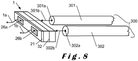
- the detector array 1 may comprise electrical connections such as electrical wires 1a, 1b, connected to said charge collecting areas as illustrated in Fig.8 .
- a SWIR detector array 1 may be configured as a linear array of SWIR detectors having said charge collecting arrays 26a, 26b arranged linearly. This can be useful for example to detect the intensity of light provided by the output surfaces of a linear array 300 of fibers.
- a SWIR detector array 1 may be configured so that each charge collecting area 26 faces the output surface of a fiber of a fiber bundle 300, as illustrated in Fig. 8 .
- the fiber bundle 300 may be arranged according to a circular arrangement or according to another arrangement such as a square, hexagonal, or rectangular arrangement.
- the invention is also realized by a SWIR detection system 3 comprising an array 300 of waveguides 301-305 and a SWIR detector array 1 as described, and of which a portion only is illustrated in Fig.10 .
- the waveguides may be fiber optics or planar waveguides.
- the waveguides may be mono-mode waveguides or multimode waveguides.
- said optical fibers are arranged in specific 2 dimensions, such as a hexagonal arrangement of fiber optics as shown in Fig.10 , or in a linear array as illustrated in Fig. 8 .
- Other geometrical configurations of the waveguides are also possible.
- a stack of flat substrates comprising each at least one waveguide may be arranged in said SWIR detection system 3.
- the cores 301a-305a of the waveguides 301-305 are facing a charge collector as illustrated in Fig. 8-10 .
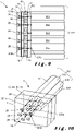
- Realizing a SWIR detection system 3 wherein the charge collectors have the same geometrical distribution than the one of the waveguide array 300, as illustrated in Figs. 9 and 10 is particularly interesting to provide an SWIR imaging system wherein an image is transferred from one end of a waveguide array 300 , such as a fiber bundle, to another end of the array. Butt-coupling a bundle of waveguides such as a fiber bundle is known to the skilled person and is not further described herein.
- optical fibers may be arranged at a predetermined distance relative to the entry face of the detector, which may be for example the contact layer 50.
- the gap layer 60 separating the entry face of the detector 1 and the outcoupling surfaces of the waveguides may be air or may be a SWIR transparent material, such as a glue layer or any other material transparent in the SWIR wavelength range.
- a gap layer may also comprise focusing lenses, such as an array of microlenses.
- the skilled person knows how to incouple light, in various ways, into a bundle of waveguides or fibers, therefore the incoupling portion of the imaging system 3, situated opposite to the outcoupling surfaces 301a-305a is not illustrated in the figures.
- the number of waveguides may be more than 100, more than 1000 or more than 10000.
- the distance between the waveguides or fibers may vary according to the application.
- the optical fibers are arranged in contact and according to a hexagonal distribution such as illustrated in Fig.10 which illustrates only 7 fibers of a closed packed optical fiber bundle.
- the detector array 1 of a SWIR detection system 3, particularly an imaging SWIR detection system 3 may comprise covered portions 36 on said buffer layer 30.
- said covered portions 36 may be realized only on etched areas 34 of the buffer layer 30 and/or may partially cover a portion of the buffer layer 30.
- Such covered portions 36 may be implemented in configurations such as the one illustrated in Fig.9 so as to reduce light cross coupling effects, which may be produced by light emitted by a waveguide and transmitted to a charge collecting area that does not face that waveguide.
- a waveguide array 300 such as a fiber bundle
- SWIR detector array By monolithically integrating a waveguide array 300, such as a fiber bundle, to a SWIR detector array, cheap and robust SWIR flexible imaging systems may be provided.
- the invention is also achieved by a method of fabrication of a short-wave infrared detector array 1 comprising a silicon readout wafer 20 having a deposition surface 20a and comprising a CMOS readout layer.
- the short-wave infrared detector array 1 comprises a slightly doped buffer layer 30 situated on said deposition surface 20a and comprises a short-wave infrared light absorption layer 40, comprising Ge and Sn, situated on said doped buffer layer 30.
- the deposition of a buffer layer 30 between the Si CMOS processed readout wafer and the absorption layer is an essential step to overcome the differences of lattices and dilatation coefficients between Si and materials such as alloys of the type Ge 1-x Sn x or Si x Ge 1-x-z Sn z .
- the method of the invention comprises the steps (A-D) of:
- said absorption layer 40 consists in a Ge 1-x Sn x alloy.
- said absorption layer 40 has a Sn content x between 0.05 ⁇ x ⁇ 0.25.
- said absorption layer 40 consists in a Si x Ge 1-x-z Sn z alloy.
- said absorption layer 40 has a Si content x between 0 ⁇ x ⁇ 0.2.
- said absorption layer 40 has a Sn content z between 0.05 ⁇ z ⁇ 0.15.
- said absorption layer 40 comprises an i-type Ge 1-x Sn x layer, in contact with said slightly doped buffer layer 30.
- said i-type Ge 1-x Sn x layer has a thickness between 250 nm and 5 ⁇ m,preferably between 250 nm and 3 ⁇ m.
- said absorption layer comprises, between said slightly doped buffer layer and said i-type Ge 1-x Sn x layer, a p + -type doped Ge 1-x Sn x layer having a doping concentration between 10 19 to 5 ⁇ 10 20 cm -3 .
- said absorption layer comprises an i-type Si x Ge 1-x-z Sn z layer, in contact with said slightly doped buffer layer 30.
- the thickness of said absorption layer 40 in all the embodiments of the invention is between 2 nm and 5 ⁇ m.
- the absorption layer 40 is realized by an epitaxial lift-off process.
- a thin film of germanium is realized on a layer of a material that can be selectively etched, for example GaAs or AIGaAs or a combination of both. This layer is then bonded on a CMOS substrate. Subsequently the GaAs or AIGaAs (or combination) is selectively etched so that the Ge is freed from the original substrate and transferred to the CMOS substrate.
- said absorption layer may be realized by successively deposited layers of Ge and Sn. These successively deposited layers may have different thicknesses.
- said slightly doped buffer layer 30 is a p-type doped Ge layer having a doping concentration between 10 14 to 10 15 cm -3 .
- said slightly doped buffer layer 30 is realized by a technology including wafer-bonding and a layer splitting process.
- a typical example of such a process is the know Smartcut process which is a Trademark as described in: http://www.soitec.com/fr/produits/smart-cut.
- Ge deposited on a substrate is implanted with hydrogen ions (H + ) with a dose comprised between 5 x 10 16 and 5 x 10 17 cm -2 and an energy comprised between 1keV and 100keV. It is then bonded to the CMOS substrate and flash annealed in order to separate the Ge layer from its substrate.
- the final structure comprises the CMOS substrate comprising a thin Ge layer that has split off from the original implanted Ge substrate.
- the implantation comprises a co-implantation with He + up to 50% of the total implanted dose of Ge and He.
- said slightly doped buffer layer 30 is realized by an epitaxial lift-off transfer process similar to the epitaxial lift-off transfer process of said absorption process as described above.
- said slightly buffer layer 30 is a p-type doped Ge 1-x Sn x layer having a doping concentration between 10 14 to 10 15 cm -3 .
- said p-type doped Ge 1-x Sn x buffer layer is realized also by said technology including wafer-bonding and a layer splitting process. Similar as described before, a typical example of such a process is the known Smartcut process (Trademark of Soitec).
- said slightly doped buffer layer is realized by an epitaxial lift-off transfer process.
- a thin film of Ge 1-x Sn x is realized on a substrate made of a material that can be selectively etched, for example GaAs or AIGaAs or a combination of both.
- the substrate is then bonded on the CMOS substrate.
- the GaAs or AIGaAs (or combination) is selectively etched so that the Ge 1-x Sn x layer is freed from the original substrate and transferred to the CMOS substrate.
- the thickness of said slightly doped buffer layer in all the embodiments of the invention is between 5 nm and 3 ⁇ m.
- said slightly doped buffer layer is etched after step B or after step C so as to provide an etched area of said slightly doped buffer layer.
- said slightly doped buffer layer is at least partially covered after step B or after step C so as to provide a selectively covered area of said slightly doped buffer layer.
- said etched area 34 is preferably covered by materials selected from: SiO x wherein 1.9 ⁇ x ⁇ 2.0, SiN, HfO, Al 2 O 3 . Said etched area 34 may also be covered by other materials that avoid the growth of a SWIR absorbing layer on the covered area.
- said selectively covered area is covered by materials selected from: SiO x , SiN, Al 2 O 3 .
- the annealing temperature of said interface layer during the annealing process step C is higher than 650°C and lower than 750°C.
- said light source provides light having a wavelength that is comprised between 300 nm and 900 nm.
- the light is provided by a pulsed light source providing light pulses having a pulse duration of said light pulses lower than 1 ms, preferably lower than 100 ns.
- the light source comprises at least one laser.
- the light source comprises at least one pulsed lamp.
- the invention is also achieved by a detector array realized according to the above described fabrication method.
- the deposition process may be achieved by different ways that determine the performance of the detector as well as the industrial scalability of its manufacturing.
- the optical layer 500 comprises an array of refractive microlens, or an array of diffractive microlenses, or an array of aspheric shaped microlenses, or an array of microprisms or an array of plasmonic planar metalenses allowing for multi/hyper-spectral imaging and analysis.
- the SWIR detector array such as a FPA
- FPA field-specific integrated circuit
- the SWIR detector array may be used in various types of applications such as ground, airborne and space technology for intelligence, surveillance, military, security or encryption systems. It may also be used for spectroscopy, machine vision or non-invasive clinical investigations such as optical coherence tomography. More precisely, the SWIR detector array can be integrated into and used in methods of the following fields of applications as described below.
- System-level benefits of large FPAs are related to providing a large instantaneous field of view and a fully electronic selection by reading out a region of interest (FOV).
- Large FPAs allow monitoring of large areas and enable key applications, such as high-resolution, wide-area airborne persistent surveillance.
- the detector larger format with smaller pixel size helps to solve the unmanned - aerial or terrestrial - vehicle (UV) automated "sense and avoid” problem.
- UV unmanned - aerial or terrestrial - vehicle
- the mechanical scanning needed in single-detector systems can be avoided and because a photon-counting FPA has the ability to digitally time stamp individual photon arrivals it is an enabler for highly sensitive light detection and ranging (“LIDAR”) imaging systems.
- LIDAR highly sensitive light detection and ranging
- each single-photon avalanche diode measures photon arrival time, and therefore depth to the corresponding point in the scene whereas the image is built up by combining multiple frames.
- Multi/ hyper-spectral LIDAR imaging can thus provide a powerful tool for mapping, archaeology, earth science, glaciology, agricultural assessment and disaster response.
Landscapes
- Engineering & Computer Science (AREA)
- Power Engineering (AREA)
- Physics & Mathematics (AREA)
- Computer Hardware Design (AREA)
- General Physics & Mathematics (AREA)
- Condensed Matter Physics & Semiconductors (AREA)
- Electromagnetism (AREA)
- Microelectronics & Electronic Packaging (AREA)
- Multimedia (AREA)
- Signal Processing (AREA)
- Health & Medical Sciences (AREA)
- Toxicology (AREA)
- Solid State Image Pick-Up Elements (AREA)
- Light Receiving Elements (AREA)
Description
- The invention relates to the manufacturing of electromagnetic radiation detector arrays for intensity detection and imaging comprising Complementary Metal Oxide Semiconductor (CMOS) circuits and absorption materials, both sensitive to high temperature. More precisely the invention relates to short-wave infrared (SWIR) detector arrays, to optical systems comprising such arrays and to methods for forming such detector arrays and also to applications thereof.
- Intensity and imaging detectors, equally named electromagnetic radiation photodiodes respectively Focal Plane Arrays (FPAs), are designed to convert the optical generation of electron-hole pairs released by impacting photons into electrical signals, further processed by a readout electronics and represented as an image on a computer screen. In addition to their high spatial and temporal resolution, these detectors also offer spectral resolution, since the energy of each incident photon is proportional to the number of generated electron-hole pairs and thus measurable by pulse height analysis.
- Intensity detector arrays and FPAs, employing direct conversion by means of semiconductor absorbers, can currently be implemented in different ways. They can first be achieved by various material depositions. Polycrystalline or amorphous materials may directly be deposited on the readout electronics made from thin film transistors, whereas single crystals - that have better transport properties - could eventually be epitaxial grown on CMOS processed readout wafers, provided specific metallization schemes will allow for high process temperatures. To the current state of knowledge, this option couldn't be realized so far.
- In a second perspective, intensity detector arrays FPAs may be integrated by various bonding processes. According to the most common one, the absorber is bonded by bump-bonding that allows for the use of any suitable semiconductor material from which large crystals may be grown, such as Si, Ge or GaAs. While with this technique it is a great challenge to push the pixel size below 50 µm, bump bonding is replaced by fusion bonding, including bonding with a patterned surface such as semiconducting pads surrounded by oxide. Both ways lead to complex structures that prevent a widespread use of the technology. By another bonding technique yet, the absorber layer and the CMOS layer are monolithically integrated by covalent bonding and subsequent annealing steps. Whereas the pixel size may be reduced by this method, according to our information, an efficient electrically conductive photodiode structure couldn't be demonstrated till now.
- In a third perspective, intensity detector arrays and FPAs may be achieved by different absorber materials that are either application or integration specific, depending on their sensitivity, absorption or manufacturability, among others. Si-based detectors can eventually be manufactured without the use of a bonding process as a high-resistivity absorber layer may be epitaxially grown directly on the CMOS Si substrate. The readout electronics is then CMOS processed in this epitaxial layer and the substrate subsequently removed [Mattiazzo, 2013]. While these detectors may be used for ionizing radiation in high-energy physics, detection in the short-wave infrared (SWIR) spectrum is not possible with Si-based absorbers. Wavelengths detection between 1.00 and 1.55 µm usually requires indium-gallium-arsenide (InGaAs) absorption materials, whereas recent studies have demonstrated that GeSn-type alloys are better candidates with a higher cutoff wavelength and a better sensitivity. Although the GeSn growth process itself can be performed at low temperature - between 300°C and 330°C - its direct growth on Si is not reliable enough because of lattices mismatch and difference in the dilatation coefficients so that the integration process requires a buffer layer. Unfortunately, as known in the art [Yeh, 2014; Aubin, 2017; Zheng 2016], this can only be obtained at high annealing temperatures.
- Thus, there is a need for a cost-effective fabrication of 3D integrated SWIR intensity detector arrays and FPA's allowing for layer deposition at temperatures compatible with CMOS substrates and other sensitive materials of the device, such as the conversion layer itself.
- Document
WO 2018/042242 shows a prior-art method of fabricating a SWIR detector array. - The invention relates to a method of fabricating an intensity detector array, in particular a short-wave infrared focal plane array (SWIR FPA), comprising a temperature sensitive conversion layer temperature sensitive a CMOS wafer, and a p-n junction in order to allow for an efficient charge collection between both layers. It is understood that the detector array has basically a p-i-n diode structure, further described as an avalanche photodiode (APD) structure including a lightly p-doped i-region. The SWIR detector array is realized by a method of fabrication comprising the deposition of a buffer layer onto the CMOS processed wafer and applying energy onto it, comprising the step of using annealing at very short light pulses duration, before providing the conversion layer on top of the buffer layer.
- It is yet a further object to provide a SWIR detector array suitable for single-photon detection and, therefore, energy-resolved SWIR detection and imaging, in which case the detector is called a focal plane array (FPA).
- It is yet another object to provide a SWIR detector array which is fabricated at temperatures compatible with the CMOS substrates and other sensitive materials of the device, such as the conversion layer itself.
- More precisely, the invention is achieved by a method of fabrication of a short-wave infrared detector array comprising a silicon readout wafer having a deposition surface and comprising a CMOS readout layer. The short-wave infrared detector array comprises a slightly doped buffer layer situated on said deposition surface and comprises a short-wave infrared light absorption layer, comprising Ge and Sn, situated on said doped buffer layer.
- The method of the invention comprises the steps (A-D) of:
- A. fabricating a readout wafer having a deposition surface, and comprising a silicon based CMOS readout layer and a p-n junction ;
- B. providing on said deposition surface a slightly doped buffer layer comprising at least Ge and having an interface layer in contact with said deposition surface, said slightly doped buffer layer comprising, to its side away from said readout wafer, an oxide-free buffer layer surface;
- C. sending light pulses, provided by a light source situated to the side of said slightly doped buffer layer opposite to said readout wafer, so as to crystallize said interface layer by the annealing effect of heat provided by the absorption of said light pulses by said interface layer, and so that a crystallized interface layer is provided and so that the temperature of the CMOS readout layer remains lower than 350°C during said annealing process;
- D. depositing on said slightly doped buffer layer, at temperatures lower than 350°C, said absorption layer.
- In an embodiment said absorption layer consists in a Ge1-xSnx alloy.
- In an embodiment said absorption layer has a Sn content x between 0.05 ≤ x ≤ 0.25.
- In an embodiment said absorption layer consists in a SixGe1-x-zSnz alloy.
- In an embodiment said absorption layer has a Si content x between 0 ≤ x ≤ 0.2.
- In embodiment said absorption layer has a Sn content z between 0.05 ≤ z ≤ 0.15.
- In an embodiment said absorption layer comprises an i-type Ge1-xSnx layer, in contact with said slightly doped buffer layer.
- In an embodiment said i-type Ge1-xSnx layer has a thickness between 250nm and 5µm, preferably between 250 µm and 3 µm.
- In an advantageous variant said absorption layer comprises, between said slightly doped buffer layer and said i-type Ge1-xSnx layer, a p+-type doped Ge1-xSnx layer having a doping concentration between 1019 to 5×1020 cm-3.
- In an embodiment said absorption layer comprises an i-type SixGe1-x-zSnz layer, in contact with said slightly doped buffer layer.
- The thickness of said absorption layer in all the embodiments of the invention is between 2 nm and 5 µm.
- In an embodiment the absorption layer is realized by an epitaxial lift-off process.
- In an embodiment said slightly doped buffer layer is a p-type doped Ge layer having a doping concentration between 1014 to 1015 cm-3.
- In an embodiment said slightly doped buffer layer is realized by a technology including wafer-bonding and a layer splitting process.
- In an embodiment said slightly doped buffer layer is realized by an epitaxial lift-off transfer process.
- In an embodiment said slightly buffer layer is a p-type doped Ge1-xSnx layer having a doping concentration between 1014 to 1015 cm-3.
- In an embodiment said p-type doped Ge1-xSnx buffer layer is realized by a technology including wafer-bonding and a layer splitting process.
- In an embodiment said buffer layer is realized by a technology including wafer-bonding and an etch back and/or polishing process.
- In an embodiment said slightly doped buffer layer is realized by an epitaxial lift-off transfer process.
- The thickness of said slightly doped buffer layer in all the embodiments of the invention is between 5 nm and 3 µm.
- In an embodiment said slightly doped buffer layer is etched after step B or after step C so as to provide an etched area of said slightly doped buffer layer.
- In an advantageous variant said slightly doped buffer layer is at least partially covered after step B or after step C so as to provide a selectively covered area of said slightly doped buffer layer.
- In an embodiment said etched area is covered by materials selected from: SiOx, SiN, Al2O3.
- In an embodiment said selectively covered area is covered by materials selected from: SiOx, SiN, Al2O3.
- In an embodiment the annealing temperature of said interface layer during the annealing process step C is higher than 650°C and lower than 750°C.
- In an embodiment said light source provides light having a wavelength that is comprised between 300 nm and 900 nm.
- In an embodiment the light is provided by a pulsed light source providing light pulses having a pulse duration of said light pulses lower than 1 ms, preferably lower than 100 ns.
- In an embodiment the light source comprises at least one laser.
- In an embodiment the light source comprises at least one pulsed lamp.
- Further details of the invention will appear more clearly upon reading the following description in reference to the appended figures:
-
Figure 1 illustrates a cross-section of an hybrid detector array of prior art having an absorber layer and a readout layer connected by bump-bonding; -
Figure 2 illustrates the temperature profile, during the annealing process step of an interface layer of a slightly doped buffer layer, across a cross-section of a CMOS processed readout wafer with, on top of it, said slightly doped buffer layer; -
Figure 3 illustrates a preferred embodiment of the SWIR detector of the invention comprising a readout wafer comprising a p-i-n diode structure, a slightly doped buffer layer and an SWIR absorption layer; -
Figure 4 illustrated the electric field across an embodiment of the SWIR detector in operation; -
Figures 5 illustrates a cross section of an embodiment of the SWIR detector of the invention in operation, the electric field across the SWIR detector and the avalanche region provided by the application of that electric field; -
Figure 6 illustrated an embodiment of the SWIR detector of the invention comprising an intrinsic layer between the slightly doped buffer layer and a doped absorber layer; -
Figure 7 illustrates an etched area in the slightly doped buffer layer of the SWIR detector; -
Figure 8 illustrates a detection system comprising a fiber array and a linear SWIR detector array comprising two charge collecting areas; -
Figure 9 illustrates a detector part of an optical detection system comprising an optical fiber array and a SWIR detector array of the invention comprising an array charge collecting areas facing the output cores of the optical fibers of the array; -
Figure 10 illustrates the image detector portion of an optical imaging system configured to transmit light intensities or an image transmitted by the bundle of fibers of the optical imaging system to the charge collecting array of the SWIR detector of said optical imaging system. -
Fig. 1 illustrates aSWIR detector array 1 of prior art. As described in the prior art such a detector array comprises typically a microlens array (A) and an absorber sheet typically made of InGaAs (B), as well as a readout circuit realized on a separate layer or wafer. The stack comprising the optical layer (A) and the absorber layer (B) is electrically and mechanically connected to the CMOS layer (C) by an array of bumps (D). - The hybrid assembly of prior art infrared detector arrays, as illustrated in
Fig.1 , requires a complex and delicate alignment process and does not allow to provide large, cheap, reliable and high efficient SWIR detector arrays. It is the aim of this invention to provide simple structures and methods for the fabrication of sensitive SWIR FPA's. - Compared to infrared detectors of prior art, the device of the invention provides a highly efficient monolithic
SWIR detector array 1 comprising a simplified 3D integrated structure having a small thickness, a reduced weight and lower power requirements. TheSWIR detector array 1 of the invention is also called a focal plane array (FPA) hereafter. The device of the invention allows to provide very sensitive and large area monolithic FPAs able to cover efficiently the whole SWIR spectrum at room-temperature or eventually Peltier-cooled operation. Said SWIR spectrum is defined by a wavelengths range between 1.0 µm and 3.0 µm. - The
SWIR detector array 1 of the invention, illustrated inFig. 3 , comprises at least: - a SWIR
light conversion layer 40, also defined as an absorber or absorption layer; - a
readout wafer 20 configured to collect, when thedetector 1 is in operation , electrical charges provided by the conversion of electromagnetic waves in electrons and holes, the electromagnetic waves having a wavelength comprised between 1.0 µm and 3.0 µm.Thereadout wafer 20 has adeposition surface 20a; - a slightly doped
buffer layer 30 comprising acrystalline interface layer 32 that is in contact with said deposition surface 20a. Saidcrystalline interface layer 32 is a thin layer made of the same chemical composition as the slightly dopedbuffer layer 30 of which it is part, and is obtained by an annealing process during the manufacturing of theSWIR detector array 1 as further described in the section related to the process of manufacturing. - The
SWIR detector array 1 of the invention may be configured to be suited for intensity measurements or as an imaging array in which case the detector array is called a Focal Plane Array as it is intended to be placed in the focal plane of an optical system. TheSWIR detector array 1 comprises also anelectrical contact layer 50 and a back contact configured to apply an electrical potential across the layers of thedetector array 1. Theelectrical contact layer 50 may be a metallic layer, a transparent conducting layer or may be a doped layer such as a highly p or n-doped layer. In an embodiment saidreadout wafer 20 is a p-doped or n-doped wafer, but not necessarily so. It is understood that the readout wafer of thedetector 1 of the invention may be configured in different ways but comprises always at least one electrical charge collecting area. In a preferred embodiment the readout wafer comprises an array of electrical charge collecting structures. The electrical charge collecting structures are preferably doped regions. The array of electrical charge collecting structures may be a 2D array, for example an array comprising 50 x 50 electrical charge collecting areas. In a variant, the array of charge collectors array may be a 1D array, comprising at least two charge collecting areas, which can be particularly useful in intensity detection applications comprising waveguides as described further. - In a variant the, 1D or 2D
SWIR detector array 1 may be made of an assembly ofSWIR detectors 1 of the invention, comprising each a low number of electrical charge collecting areas, for example 10 electrical charge collecting areas perdetector array 1. In a particular case wherein the spacing of the electrical charge areas may be relatively high, for example greater than 100 µm as illustrated inFig. 8 , thedetector array 1 may comprise widely spaced charge collecting areas. In the case of imaging applications thedetector array 1 is a FPA comprising densely packed charge collecting areas, as illustrated inFig. 5 illustrating a single pixel of a FPA. -
Fig. 4 illustrates the electrical field across an embodiment of theSWIR detector array 1 in operation. In operation, the electrical potential drop across thedetector array 1 produces an electrical field E, illustrated in the graph ofFig. 4. Fig. 4 illustrates also an avalanche region (AV) provided by an electrical field E applied across thedetector array 1. The extent of the avalanche region (AV) across theSWIR detector 1 in operation and depends on the particular configuration of theSWIR detector 1 and is therefore shown as an arrow (AV). - In a typical realization, the readout electronics is preferably processed in an epitaxial Si layer with a thickness of about 10 - 30 µm and a resistivity above about 500 Qcm or preferably about 1 - 2 kΩcm or more preferably 2 - 5 kΩ2cm or even above 5 kΩcm, for example 5 - 50 kΩcm, the resistivity being due to a low doping level in between about 1011 to 1013 cm-3 of a first conduction type (for example n-conduction induced by n-doping). For ease of detector manufacturing, silicon-on-insulator (SOI) wafers may be used for the CMOS processing of the readout electronics. The thickness and the material used for the absorption layer strongly depends on the energy of the electromagnetic radiation to be detected.
- An exemplary cross section of an embodiment of the
readout layer 20, comprising ap-n diode layer 22, is illustrated inFig. 5 . As illustrated in the cross section ofFig. 5 , asilicon layer 20 may comprisen+ charge collectors 24. In a preferred embodiment saidabsorption layer 40 is a lightly p-doped layer. In operation, each photon incident on theabsorption layer 40 creates an electron-hole pair in theabsorber 40. The hole is collected at the incident light side and the electron, created by the absorption of a photon, drifts to the avalanche region AV (Fig. 4 ) situated to the side of the p-n junction and is accelerated to sufficient energy to initiate a chain of impact ionization events, creating offspring electron-hole pairs and leading to internal gain. In the Geiger mode, known to the person skilled in the art, in which single photon can initiate an avalanche that is self-sustaining, carrier generation predominates over extraction leading to exponential growth of the current. In this mode the detector array has to be electrically reset by reducing the bias to below breakdown long enough to terminate the avalanche, a process known as quenching. Thus, when a reverse bias is applied to the back contact of the detector, the space charge layer expands from thep-n junction 22, as illustrated infigure 4 , into thereadout wafer 20, into said slight dopedbuffer layer 30 and as well as in the, preferable p-conducting,absorption layer 40.Figure 4 illustrates also the electric field E across the detector when a reverse bias is applied to a back contact of thedetector array 1. - By construction, the
SWIR detector array 1, such as a FPA of the invention provides single-photon detection. It is therefore suitable for energy discrimination, whereby the energy of photons incident on the absorber can be measured by employing the pulse height analysis of the electrical pulses processed by the readout electronics. - In an embodiment said
buffer layer 30 consists of a slightly doped Ge layer and is preferably a p-type doped Ge layer having a doping concentration between 1014 to 1015 cm-3. - In an embodiment said slightly doped
buffer layer 30 is made of Ge1-xSnx and has a Sn content x between 0.00 ≤ x ≤ 0.03, and is preferably a p-type doped Ge1-xSnx layer having a doping concentration between 1014 to 1015 cm-3. - As further described, said slightly doped
buffer layer 30 may be advantageously be realized by an epitaxial lift-off transfer process. - In an embodiment said buffer layer (30 is realized by a technology including wafer-bonding and an etch back and/or a polishing process.
- In an advantageous embodiment said
absorption layer 40 consists in a Ge1-xSnx alloy. Saidabsorption layer 40 has preferably a Sn content x between 0.05 ≤ x ≤ 0.25. - In an embodiment said
absorption layer 40 consists in a SixGe1-x-zSnz alloy and has preferably a Si content x between 0 ≤ x ≤ 0.2. - In an embodiment of the
absorption layer 40 consisting in a SixGe1-x-zSnz alloy saidabsorption layer 40 has a Sn content z between 0.05 ≤ z ≤ 0.15. - In an advantageous embodiment said
absorption layer 40 comprises an i-type Ge1-xSnx layer 42 being in contact with said slightly dopedbuffer layer 30. This layer can absorb up to 100% of the incident light with a photon wavelength greater than 1.4 µm, depending on the thickness. - Said i-type Ge1-xSnx layer may have a thickness between 250 nm and 5 µm, preferably between 250 nm and 3 µm.
- In a variant of execution, illustrated in
figure 6 , saidabsorption layer 40 comprises, between said slightly dopedbuffer layer 30 and said i-type Ge1-xSnx layer 42, a p+-type doped Ge1-xSnx layer 44 having a doping concentration between 1019 to 5 ×1020 cm-3. - In an embodiment said
absorption layer 40 comprises an i-type SixGe1-x-zSnz layer, in contact with said slightly dopedbuffer layer 30. - In a variant of execution, similar to the arrangement of the embodiment of
figure 6 , saidabsorption layer 40 comprises, between said slightly dopedbuffer layer 30 and said i-type SixGe1-x-zSnz layer, a p+-type doped Ge1-xSnx layer having a doping concentration between 1019 to 5x1020 cm-3. - In all embodiments the thickness of the
absorption layer 40 is between 2 nm and 5 µm.In a variant, the thickness of theabsorption layer 40 is between 1nm and 1000µm. - In variants, as illustrated in
Fig. 7 , an etchedarea 34 may be provided in thebuffer layer 30. This etchedarea 34 extends across the whole thickness of thebuffer layer 30 and may serve to deposit other materials, different to the buffer material, directly on saiddeposition surface 20a. These added other materials my serve to avoid the growth of absorption alloys such as Ge1-xSnx and SixGe1-x-zSnz over predetermined areas. - In an embodiment said etched
area 34 may be covered by materials selected from: SiOx wherein 1.9<x<2.0, SiN, HfO, Al2O3. Said coverage is not limited to these materials. - Also, a portion of the
buffer layer 30 may also comprise a selectively covered area that is covered by materials selected from: SiOx wherein 1.9 < x < 2.0, SiN, HfO, Al2O3. These added other materials my serve to avoid the growth of absorption alloys such as Ge1-xSnx and SixGe1-x-zSnz on the whole extension of the buffer layer. - In an embodiment at least a portion of said etched
area 34 and a portion of saidbuffer layer 30 may be covered by materials selected from: SiOx wherein 1.9 < x < 2.0, SiN, HfO, Al2O3. In a variant said etchedarea 34 and a portion of saidbuffer layer 30 are covered by different materials. - It is understood that further layers than the ones described before may be added to the SWIR detector array, either between said
readout wafer 20 and thebuffer layer 30 as between thebuffer layer 30 and theabsorption layer 40. - For example, an optical layer having optical focusing properties may be arranged between said
absorption layer 40 and said buffer layer. For example, at least one side of saidabsorption layer 30 may be corrugated and have for example the shape of an array of microlenses so as to provide a focused light beam on a focal plane coincident with saidinterfacial layer 32. In the variant in which theabsorption layer 30 is structured or corrugated to the side of saidreadout wafer 20, theinterface layer 32 will have the same structured or corrugated shape as the structured or corrugated surface of saidabsorption layer 30. - In an embodiment an antireflection coating is added in order to maximize the amount of light coupled into the device/absorbing layer.
- Depending on the desired electrical performances of the
detector array 1 the composition and thickness of any of the layers of thedetector 1 may be configured so as to shape a predetermined electrical field profile across the avalanche region (AV) of thedetector 1. Shaping electrical field profiles is well known in the art and is not further commented here. - An exemplary execution of a small part of the cross-section of the thinned CMOS processed
readout wafer 20 of aSWIR detector array 1 comprises ap-n junction 22 is now described and illustrated inFig. 5 . The width of the section illustrated infigure 5 , defined in the plane of thereadout wafer 21, corresponds to slightly more than a single pixel size of thedetector array 1, and may range for example from 5 -20 µm,20 - 50 µm,50 -100 µm, depending on the CMOS process used. In this configuration, n-wells 25 serve as charge collectors, collecting electrons coming from electron-hole pairs which are generated by incident photons and separated in the electric field of the p-n junction formed by a preferably lightly n-doped Si CMOS processesreadout wafer 20 and a lightly p-doped layer. The distance between adjacent n-wells 25 defines the pixel size of the detector array. In the embodiment offigure 5 , n-MOS transistors of the pixel electronics of the readout are situated in p-wells 26 and n-wells 23, respectively. A deep p-well 24 arranged on said p-wells 26 and n-wells 23, has the purpose of avoiding electron collection by n-wells 23 in addition to charge collecting by n-well 25. In an aspect of the embodiment part of the pixel electronics may be located in n-well 25. In this configuration thep-n junction 22 is inside the readout wafer, preferably at the interface between a lightly p-doped layer and a lightly n-doped main part ofSOI wafer 20. The lightly n-doped main part ofSOI wafer 20 comprises preferably a thin, lightly p-doped Si layer with a highly resistive n-doped layer on top, hosting the CMOS processed readout. The lightly p-doped layer may have a thickness of about 1- 2 µm, 2 - 5 µm or even in the range from 5 - 50 µm or 50 - 100 µm. Substrate and buried oxide of the SOI wafer are thereby removed prior to further processing of the device. - It has to be noticed that in variants the
detector array 1 may comprise electrical connections such aselectrical wires Fig.8 . - In an example, illustrated in
Fig. 8 , aSWIR detector array 1 may be configured as a linear array of SWIR detectors having saidcharge collecting arrays linear array 300 of fibers. In the same way, aSWIR detector array 1 may be configured so that eachcharge collecting area 26 faces the output surface of a fiber of afiber bundle 300, as illustrated inFig. 8 . Thefiber bundle 300 may be arranged according to a circular arrangement or according to another arrangement such as a square, hexagonal, or rectangular arrangement. The advantage of realizing adetector array 1 havingcharge collecting areas 26 having the same geometric distribution as the output surfaces of the fibers of afiber bundle 300, allows to avoid using imaging optics between the output surfaces of the waveguides and the charge collectors. It is understood that, rather than fiber optics, flat optical waveguides may be used of which each output surface faces a charge collecting area of thedetector array 1. It is also understood that in all embodiments of thedetector array 1, at least one electrical wire may be connected to theCMOS layer 21, and more precisely to at least one charge collecting area as illustrated in the example ofFig.8 . - The invention is also realized by a
SWIR detection system 3 comprising anarray 300 of waveguides 301-305 and aSWIR detector array 1 as described, and of which a portion only is illustrated inFig.10 . The waveguides may be fiber optics or planar waveguides. In variants the waveguides may be mono-mode waveguides or multimode waveguides. In a variant said optical fibers are arranged in specific 2 dimensions, such as a hexagonal arrangement of fiber optics as shown inFig.10 , or in a linear array as illustrated inFig. 8 . Other geometrical configurations of the waveguides are also possible. In a variant a stack of flat substrates comprising each at least one waveguide may be arranged in saidSWIR detection system 3. - In embodiments the
cores 301a-305a of the waveguides 301-305 are facing a charge collector as illustrated inFig. 8-10 . Realizing aSWIR detection system 3 wherein the charge collectors have the same geometrical distribution than the one of thewaveguide array 300, as illustrated inFigs. 9 and 10 is particularly interesting to provide an SWIR imaging system wherein an image is transferred from one end of awaveguide array 300 , such as a fiber bundle, to another end of the array. Butt-coupling a bundle of waveguides such as a fiber bundle is known to the skilled person and is not further described herein. For example, as shown inFig.9 , optical fibers may be arranged at a predetermined distance relative to the entry face of the detector, which may be for example thecontact layer 50. Thegap layer 60 separating the entry face of thedetector 1 and the outcoupling surfaces of the waveguides may be air or may be a SWIR transparent material, such as a glue layer or any other material transparent in the SWIR wavelength range. A gap layer may also comprise focusing lenses, such as an array of microlenses. Also, the skilled person knows how to incouple light, in various ways, into a bundle of waveguides or fibers, therefore the incoupling portion of theimaging system 3, situated opposite to theoutcoupling surfaces 301a-305a is not illustrated in the figures. - In an exemplary realization the number of waveguides may be more than 100, more than 1000 or more than 10000. The distance between the waveguides or fibers may vary according to the application. In an exemplary configuration the optical fibers are arranged in contact and according to a hexagonal distribution such as illustrated in
Fig.10 which illustrates only 7 fibers of a closed packed optical fiber bundle. - In a variant, the
detector array 1 of aSWIR detection system 3, particularly an imagingSWIR detection system 3, may comprise coveredportions 36 on saidbuffer layer 30. As explained further, said coveredportions 36 may be realized only on etchedareas 34 of thebuffer layer 30 and/or may partially cover a portion of thebuffer layer 30. Suchcovered portions 36 may be implemented in configurations such as the one illustrated inFig.9 so as to reduce light cross coupling effects, which may be produced by light emitted by a waveguide and transmitted to a charge collecting area that does not face that waveguide. - By monolithically integrating a
waveguide array 300, such as a fiber bundle, to a SWIR detector array, cheap and robust SWIR flexible imaging systems may be provided. - The assembly of fiber bundles or waveguides with detectors and detector arrays are known to the skilled person and are not described further here.
- The invention is also achieved by a method of fabrication of a short-wave
infrared detector array 1 comprising asilicon readout wafer 20 having adeposition surface 20a and comprising a CMOS readout layer. The short-waveinfrared detector array 1 comprises a slightly dopedbuffer layer 30 situated on saiddeposition surface 20a and comprises a short-wave infraredlight absorption layer 40, comprising Ge and Sn, situated on saiddoped buffer layer 30. The deposition of abuffer layer 30 between the Si CMOS processed readout wafer and the absorption layer is an essential step to overcome the differences of lattices and dilatation coefficients between Si and materials such as alloys of the type Ge1-xSnx or SixGe1-x-zSnz. - More precisely the method of the invention comprises the steps (A-D) of:
- A. fabricating a
readout wafer 20 having adeposition surface 20a, and comprising a silicon basedCMOS readout layer 21 and ap-n junction 22; - B. providing on said
deposition surface 20a a slightly dopedbuffer layer 30 comprising at least Ge and having aninterface layer 32 in contact with saiddeposition surface 20a, said slightly dopedbuffer layer 30 comprising, to its side away from saidreadout wafer 20, an oxide-freebuffer layer surface 30a ; - C. sending
light pulses 200, provided by a light source situated to the side of said slightly doped buffer layer opposite to said readout wafer, so as to crystallize said interface layer by the annealing effect of heat provided by the absorption of said light pulses by saidinterface layer 32, and so that acrystallized interface layer 32 is provided and so that the temperature of theCMOS readout layer 21 remains lower than 350°C during said annealing process; - D. depositing on said slightly doped
buffer layer 30, at temperatures lower than 350°C, saidabsorption layer 40. - In an embodiment said
absorption layer 40 consists in a Ge1-xSnx alloy. - In an embodiment said
absorption layer 40 has a Sn content x between 0.05 ≤ x ≤ 0.25. - In an embodiment said
absorption layer 40 consists in a SixGe1-x-zSnz alloy. - In an embodiment said
absorption layer 40 has a Si content x between 0 ≤ x ≤ 0.2. - In an embodiment said
absorption layer 40 has a Sn content z between 0.05 ≤ z ≤ 0.15. - In an embodiment said
absorption layer 40 comprises an i-type Ge1-xSnx layer, in contact with said slightly dopedbuffer layer 30. - In an embodiment said i-type Ge1-xSnx layer has a thickness between 250 nm and 5 µm,preferably between 250 nm and 3 µm.
- In an advantageous variant said absorption layer comprises, between said slightly doped buffer layer and said i-type Ge1-xSnx layer, a p+-type doped Ge1-xSnx layer having a doping concentration between 1019 to 5×1020 cm-3.
- In an embodiment, said absorption layer comprises an i-type SixGe1-x-zSnz layer, in contact with said slightly doped
buffer layer 30. - The thickness of said
absorption layer 40 in all the embodiments of the invention is between 2 nm and 5 µm. - In an embodiment the
absorption layer 40 is realized by an epitaxial lift-off process. In such an epitaxial lift-off process a thin film of germanium is realized on a layer of a material that can be selectively etched, for example GaAs or AIGaAs or a combination of both. This layer is then bonded on a CMOS substrate. Subsequently the GaAs or AIGaAs (or combination) is selectively etched so that the Ge is freed from the original substrate and transferred to the CMOS substrate. - In a variant said absorption layer may be realized by successively deposited layers of Ge and Sn. These successively deposited layers may have different thicknesses.
- In an embodiment said slightly doped
buffer layer 30 is a p-type doped Ge layer having a doping concentration between 1014 to 1015 cm-3. - In an embodiment said slightly doped
buffer layer 30 is realized by a technology including wafer-bonding and a layer splitting process. A typical example of such a process is the know Smartcut process which is a Trademark as described in: http://www.soitec.com/fr/produits/smart-cut. - In such a process Ge deposited on a substrate, and is implanted with hydrogen ions (H+) with a dose comprised between 5 x 10¹⁶ and 5 x 1017 cm-2 and an energy comprised between 1keV and 100keV. It is then bonded to the CMOS substrate and flash annealed in order to separate the Ge layer from its substrate. The final structure comprises the CMOS substrate comprising a thin Ge layer that has split off from the original implanted Ge substrate. In a variant, the implantation comprises a co-implantation with He+ up to 50% of the total implanted dose of Ge and He.
- In an embodiment said slightly doped
buffer layer 30 is realized by an epitaxial lift-off transfer process similar to the epitaxial lift-off transfer process of said absorption process as described above. - In an embodiment said slightly
buffer layer 30 is a p-type doped Ge1-xSnx layer having a doping concentration between 1014 to 1015 cm-3. - In an embodiment said p-type doped Ge1-xSnx buffer layer is realized also by said technology including wafer-bonding and a layer splitting process. Similar as described before, a typical example of such a process is the known Smartcut process (Trademark of Soitec).
- In an embodiment said slightly doped buffer layer is realized by an epitaxial lift-off transfer process. In such an epitaxial lift-off transfer process a thin film of Ge1-xSnx is realized on a substrate made of a material that can be selectively etched, for example GaAs or AIGaAs or a combination of both. The substrate is then bonded on the CMOS substrate. Subsequently the GaAs or AIGaAs (or combination) is selectively etched so that the Ge1-xSnx layer is freed from the original substrate and transferred to the CMOS substrate.
- The thickness of said slightly doped buffer layer in all the embodiments of the invention is between 5 nm and 3 µm.
- In an embodiment said slightly doped buffer layer is etched after step B or after step C so as to provide an etched area of said slightly doped buffer layer.
- In an advantageous variant said slightly doped buffer layer is at least partially covered after step B or after step C so as to provide a selectively covered area of said slightly doped buffer layer.
- In an embodiment said etched
area 34 is preferably covered by materials selected from: SiOx wherein 1.9 < x < 2.0, SiN, HfO, Al2O3. Said etchedarea 34 may also be covered by other materials that avoid the growth of a SWIR absorbing layer on the covered area. - In an embodiment said selectively covered area is covered by materials selected from: SiOx, SiN, Al2O3.
- In an embodiment the annealing temperature of said interface layer during the annealing process step C is higher than 650°C and lower than 750°C.
- In an embodiment said light source provides light having a wavelength that is comprised between 300 nm and 900 nm.
- In an embodiment the light is provided by a pulsed light source providing light pulses having a pulse duration of said light pulses lower than 1 ms, preferably lower than 100 ns.
- In an embodiment the light source comprises at least one laser.
- In an embodiment the light source comprises at least one pulsed lamp.
- The invention is also achieved by a detector array realized according to the above described fabrication method.
- The deposition process may be achieved by different ways that determine the performance of the detector as well as the industrial scalability of its manufacturing.
- In variants the
optical layer 500 comprises an array of refractive microlens, or an array of diffractive microlenses, or an array of aspheric shaped microlenses, or an array of microprisms or an array of plasmonic planar metalenses allowing for multi/hyper-spectral imaging and analysis. - The SWIR detector array, such as a FPA, may be used in various types of applications such as ground, airborne and space technology for intelligence, surveillance, military, security or encryption systems. It may also be used for spectroscopy, machine vision or non-invasive clinical investigations such as optical coherence tomography. More precisely, the SWIR detector array can be integrated into and used in methods of the following fields of applications as described below.
- System-level benefits of large FPAs are related to providing a large instantaneous field of view and a fully electronic selection by reading out a region of interest (FOV). Large FPAs allow monitoring of large areas and enable key applications, such as high-resolution, wide-area airborne persistent surveillance. The detector larger format with smaller pixel size helps to solve the unmanned - aerial or terrestrial - vehicle (UV) automated "sense and avoid" problem. By using an array of detectors in a FPA, the mechanical scanning needed in single-detector systems can be avoided and because a photon-counting FPA has the ability to digitally time stamp individual photon arrivals it is an enabler for highly sensitive light detection and ranging ("LIDAR") imaging systems. In a LIDAR system the scene is illuminated by a short laser pulse, and imaged onto the FPA, where each single-photon avalanche diode measures photon arrival time, and therefore depth to the corresponding point in the scene whereas the image is built up by combining multiple frames.
- Most minerals contain distinct absorption features in the SWIR, making this region of the spectrum the best candidate for spectroscopic analysis in many applications. Hydroxyl bearing minerals, sulfates, and carbonate materials produced naturally on earth - or directly related to human activities such as the burning of fossil fuels and the deforestation - are easily identified through SWIR spectroscopy. Multi/ hyper-spectral LIDAR imaging can thus provide a powerful tool for mapping, archaeology, earth science, glaciology, agricultural assessment and disaster response.
- There are a wide range of applications wherein a direct image may not be formed on a detector array. For example this is the case wherein difficult accessible places have to be imaged. The use of imaging systems using a bundle of fibers or flexible flat waveguides may be mandatory. Applications may be found for example in the field of industrial endoscopes for example to inspect the inside of tubings.
-
- 1. Aubin J. et al., "Impact of thickness on the structural properties of high tin content GeSn layers", Journal of Crystal Growth, 473, 20-27, 2017
- 2. Lee J. et al., "Crystallization and Characterization of GeSn Deposited on Si with Ge Buffer Layer by Low-temperature Sputter Epitaxy, Journal of Semiconductor Technology and Science, Vol. 16, No 6, December 2016
- 3. Mattiazzo S. et al., "LePIX: first results from a novel monolithic sensor", Nucl. Instr. Meth. Phys. Res. A 718, 288-291, 2013
- 4. Yeh W. et al., "Sputter Epitaxial Growth of Flat Germanium Film with Low Threading-Dislocation Density on Silicon (001)", ECS journal of Solid State Science and Technology, 3 (10) Q195-Q199, 1 Aug 2014
- 5. Zahler J.M. et al " Role of hydrogen in hydrogen-induced layer exfoliation of germanium" Phys. Rev. B 75, 035309, 2007
- 6. Zheng J. et al., "GeSn p-i-n photodetectors with GeSn layer grown by magnetron sputtering epitaxy", Appl. Phys.
Claims (14)
- A method of fabrication of a short-wave infrared detector array (1) comprising a silicon readout wafer (20), having a deposition surface (20a), comprising a CMOS readout layer (21) comprising at least two charge collecting structures, said short-wave infrared detector array (1) comprising a slightly doped buffer layer (30) situated on said deposition surface (20a) and a short-wave infrared light absorption layer (40), comprising Ge and Sn, situated on said doped buffer layer (30),
the method comprising the steps (A-D) of:A. fabricating a readout wafer (20) having a deposition surface (20a), and comprising a silicon based CMOS readout layer (21) and a p-n junction (22);B. providing on said deposition surface (20a) a slightly doped buffer layer (30) comprising at least Ge and having an interface layer (32) in contact with said deposition surface (20a), said slightly doped buffer layer (30) comprising to its side away from said readout wafer (20), an oxide-free buffer layer surface (30a);C. sending light pulses (200), provided by a light source situated to the side of said slightly doped buffer layer (30) opposite to said readout wafer (20), so as to crystallize said interface layer (32) by the annealing effect of heat provided by the absorption of said light pulses (200) by said interface layer (32), and so that temperature of the CMOS readout layer (21) remains lower than 350°C during the annealing process;D. depositing on said slightly doped buffer layer (30), at temperatures lower than 350°C, said absorption layer (40). - The method according to claim 1 wherein said absorption layer (40) comprises an i-type Ge1-xSnx layer, in contact with said slightly doped buffer layer (30).
- The method according to claim 2 wherein said i-type Ge1-xSnx layer has a thickness between 250nm and 5µm, preferably between 250nm and 3µm.
- The method according to claims 2 or 3 wherein said absorption layer (40) comprises, between said slightly doped buffer layer (30) and said i-type Ge1-xSnx layer, a p+-type doped Ge1-xSnx layer having a doping concentration between 1019 to 5×1020 cm-3.
- The method according to any one of claims 1 to 4 wherein the absorption layer (40) is realized by an epitaxial lift-off process.
- The method according to any one of claims 1 to 5 wherein said slightly doped buffer layer (30) is a p-type doped Ge layer having a doping concentration between 1014 to 1015 cm-3.
- The method according to any one of claims 1 to 6 wherein said slightly doped buffer layer (30) is realized by a technology including wafer-bonding and a layer splitting process.
- The method according to any one of claims 1 to 6 wherein said slightly doped buffer layer (30) is realized by a technology including wafer-bonding and an etch back and/or polishing process.
- The method according to any one of claims 1 to 6 wherein said slightly doped buffer layer (30) is realized by an epitaxial lift-off transfer process.
- The method according to any one of claims 1 to 9 wherein said slightly doped buffer layer (30) is a p-type doped Ge1-xSnx layer having a doping concentration between 1014 to 1015 cm-3.
- The method according to claim 10 wherein said p-type doped Ge1-xSnx buffer layer (30) is realized by a technology including wafer-bonding and a layer splitting process.
- The method according to any one of claims 1 to 11 wherein the thickness of said slightly doped buffer layer (30) is between 5 nm and 3 µm.
- The method according to any one of claims 1 to 12 wherein said slightly doped buffer layer (30) is etched after step B or after step C so as to provide an etched area (34) of the buffer layer (30).
- The method according to any one of claims 1 to 13 wherein the light is provided by a pulsed light source providing light pulses (200) having a pulse duration of said light pulses (200) lower than 1 ms, preferably lower than 100 ns.
Applications Claiming Priority (1)
| Application Number | Priority Date | Filing Date | Title |
|---|---|---|---|
| PCT/EP2018/062763 WO2019219189A1 (en) | 2018-05-16 | 2018-05-16 | Short-wave infrared detector and its integration with cmos compatible substrates |
Publications (2)
| Publication Number | Publication Date |
|---|---|
| EP3794643A1 EP3794643A1 (en) | 2021-03-24 |
| EP3794643B1 true EP3794643B1 (en) | 2022-06-22 |
Family
ID=62222645
Family Applications (1)
| Application Number | Title | Priority Date | Filing Date |
|---|---|---|---|
| EP18726412.2A Active EP3794643B1 (en) | 2018-05-16 | 2018-05-16 | Integration of a short-wave infrared detector with cmos compatible substrates |
Country Status (3)
| Country | Link |
|---|---|
| US (1) | US20210210544A1 (en) |
| EP (1) | EP3794643B1 (en) |
| WO (1) | WO2019219189A1 (en) |
Families Citing this family (3)
| Publication number | Priority date | Publication date | Assignee | Title |
|---|---|---|---|---|
| EP3738147B1 (en) * | 2018-01-12 | 2021-11-24 | IRIS Industries SA | Short-wave infrared detector and its integration with cmos compatible substrates |
| CN111708044B (en) * | 2020-06-20 | 2021-07-06 | 桂林理工大学 | Airborne supercontinuum laser 50-waveband hyperspectral radar system |
| US20230041955A1 (en) * | 2021-08-05 | 2023-02-09 | Sri International | Sensor with upconversion layer |
Family Cites Families (5)
| Publication number | Priority date | Publication date | Assignee | Title |
|---|---|---|---|---|
| US7651880B2 (en) * | 2006-11-04 | 2010-01-26 | Sharp Laboratories Of America, Inc. | Ge short wavelength infrared imager |
| US20090020700A1 (en) * | 2007-07-17 | 2009-01-22 | Locheed Martin Corporation | Method and device for generating an electrical signal in response to light |
| CN102280456B (en) * | 2011-05-11 | 2013-06-26 | 北京大学 | Infrared focal plane array seeker integrated structure and manufacturing method |
| US9472588B1 (en) * | 2015-06-19 | 2016-10-18 | International Business Machines Corporation | Monolithic visible-infrared focal plane array on silicon |
| KR102046980B1 (en) * | 2016-08-31 | 2019-11-20 | 쥐-레이 스위츨란드 에스에이 | Electromagnetic radiation detector with charge transport across the bonding interface |
-
2018
- 2018-05-16 EP EP18726412.2A patent/EP3794643B1/en active Active
- 2018-05-16 US US17/055,269 patent/US20210210544A1/en not_active Abandoned
- 2018-05-16 WO PCT/EP2018/062763 patent/WO2019219189A1/en unknown
Also Published As
| Publication number | Publication date |
|---|---|
| US20210210544A1 (en) | 2021-07-08 |
| WO2019219189A1 (en) | 2019-11-21 |
| EP3794643A1 (en) | 2021-03-24 |
Similar Documents
| Publication | Publication Date | Title |
|---|---|---|
| US10854656B2 (en) | Short-wave infrared detector array and method for the manufacturing thereof | |
| EP2403011B1 (en) | Semiconductor light-detecting element | |
| US9076702B2 (en) | Frontside-illuminated barrier infrared photodetector device and methods of fabricating the same | |
| JP5829224B2 (en) | MOS image sensor | |
| EP3794643B1 (en) | Integration of a short-wave infrared detector with cmos compatible substrates | |
| US20130043372A1 (en) | Multi-Band Position Sensitive Imaging Arrays | |
| EP3738147B1 (en) | Short-wave infrared detector and its integration with cmos compatible substrates | |
| US7795639B2 (en) | Avalanche photodiode | |
| DE102012214690A1 (en) | Electromagnetic radiation detector for wide-band multi-spectral imaging device, has lower detection structure that is arranged within lower semiconductor chip to overlap with upper detection structure arranged within upper chip | |
| KR102153209B1 (en) | Direct read pixel alignment | |
| KR102467958B1 (en) | Germanium-Based Focal Plane Arrays for Shortwave Infrared Spectral Schemes | |
| US11133349B2 (en) | Short-wave infrared detector array and fabrication methods thereof | |
| Sood et al. | Characterization of SiGe-detector arrays for visible-NIR imaging sensor applications | |
| RU2530458C1 (en) | METHOD OF PRODUCING MULTIELEMENT PHOTODETECTOR BASED ON EPITAXIAL InGaAs/InP STRUCTURES | |
| Sood et al. | Development of low dark current SiGe-detector arrays for visible-NIR Imaging Sensor | |
| Sood et al. | Development of SiGe arrays for visible-near IR applications | |
| Nanver et al. | Optical detectors | |
| US20240304637A1 (en) | Image sensors and method of manufacturing the same | |
| KR20240136073A (en) | Image sensors and method of manufacturing the same |
Legal Events
| Date | Code | Title | Description |
|---|---|---|---|
| STAA | Information on the status of an ep patent application or granted ep patent |
Free format text: STATUS: UNKNOWN |
|
| STAA | Information on the status of an ep patent application or granted ep patent |
Free format text: STATUS: THE INTERNATIONAL PUBLICATION HAS BEEN MADE |
|
| STAA | Information on the status of an ep patent application or granted ep patent |
Free format text: STATUS: THE INTERNATIONAL PUBLICATION HAS BEEN MADE |
|
| PUAI | Public reference made under article 153(3) epc to a published international application that has entered the european phase |
Free format text: ORIGINAL CODE: 0009012 |
|
| STAA | Information on the status of an ep patent application or granted ep patent |
Free format text: STATUS: REQUEST FOR EXAMINATION WAS MADE |
|
| 17P | Request for examination filed |
Effective date: 20201106 |
|
| AK | Designated contracting states |
Kind code of ref document: A1 Designated state(s): AL AT BE BG CH CY CZ DE DK EE ES FI FR GB GR HR HU IE IS IT LI LT LU LV MC MK MT NL NO PL PT RO RS SE SI SK SM TR |
|
| AX | Request for extension of the european patent |
Extension state: BA ME |
|
| RIN1 | Information on inventor provided before grant (corrected) |
Inventor name: FONTCUBERTA MORRAL, ANNA Inventor name: CHUNG, MINTAE |
|
| DAV | Request for validation of the european patent (deleted) | ||
| DAX | Request for extension of the european patent (deleted) | ||
| GRAP | Despatch of communication of intention to grant a patent |
Free format text: ORIGINAL CODE: EPIDOSNIGR1 |
|
| STAA | Information on the status of an ep patent application or granted ep patent |
Free format text: STATUS: GRANT OF PATENT IS INTENDED |
|
| INTG | Intention to grant announced |
Effective date: 20220211 |
|
| GRAS | Grant fee paid |
Free format text: ORIGINAL CODE: EPIDOSNIGR3 |
|
| GRAA | (expected) grant |
Free format text: ORIGINAL CODE: 0009210 |
|
| STAA | Information on the status of an ep patent application or granted ep patent |
Free format text: STATUS: THE PATENT HAS BEEN GRANTED |
|
| AK | Designated contracting states |
Kind code of ref document: B1 Designated state(s): AL AT BE BG CH CY CZ DE DK EE ES FI FR GB GR HR HU IE IS IT LI LT LU LV MC MK MT NL NO PL PT RO RS SE SI SK SM TR |
|
| REG | Reference to a national code |
Ref country code: GB Ref legal event code: FG4D |
|
| REG | Reference to a national code |
Ref country code: CH Ref legal event code: EP |
|
| REG | Reference to a national code |
Ref country code: DE Ref legal event code: R096 Ref document number: 602018037010 Country of ref document: DE |
|
| REG | Reference to a national code |
Ref country code: AT Ref legal event code: REF Ref document number: 1500346 Country of ref document: AT Kind code of ref document: T Effective date: 20220715 |
|
| REG | Reference to a national code |
Ref country code: IE Ref legal event code: FG4D |
|
| REG | Reference to a national code |
Ref country code: LT Ref legal event code: MG9D |
|
| REG | Reference to a national code |
Ref country code: NL Ref legal event code: MP Effective date: 20220622 |
|
| PG25 | Lapsed in a contracting state [announced via postgrant information from national office to epo] |
Ref country code: SE Free format text: LAPSE BECAUSE OF FAILURE TO SUBMIT A TRANSLATION OF THE DESCRIPTION OR TO PAY THE FEE WITHIN THE PRESCRIBED TIME-LIMIT Effective date: 20220622 Ref country code: NO Free format text: LAPSE BECAUSE OF FAILURE TO SUBMIT A TRANSLATION OF THE DESCRIPTION OR TO PAY THE FEE WITHIN THE PRESCRIBED TIME-LIMIT Effective date: 20220922 Ref country code: LT Free format text: LAPSE BECAUSE OF FAILURE TO SUBMIT A TRANSLATION OF THE DESCRIPTION OR TO PAY THE FEE WITHIN THE PRESCRIBED TIME-LIMIT Effective date: 20220622 Ref country code: HR Free format text: LAPSE BECAUSE OF FAILURE TO SUBMIT A TRANSLATION OF THE DESCRIPTION OR TO PAY THE FEE WITHIN THE PRESCRIBED TIME-LIMIT Effective date: 20220622 Ref country code: GR Free format text: LAPSE BECAUSE OF FAILURE TO SUBMIT A TRANSLATION OF THE DESCRIPTION OR TO PAY THE FEE WITHIN THE PRESCRIBED TIME-LIMIT Effective date: 20220923 Ref country code: FI Free format text: LAPSE BECAUSE OF FAILURE TO SUBMIT A TRANSLATION OF THE DESCRIPTION OR TO PAY THE FEE WITHIN THE PRESCRIBED TIME-LIMIT Effective date: 20220622 Ref country code: BG Free format text: LAPSE BECAUSE OF FAILURE TO SUBMIT A TRANSLATION OF THE DESCRIPTION OR TO PAY THE FEE WITHIN THE PRESCRIBED TIME-LIMIT Effective date: 20220922 |
|
| REG | Reference to a national code |
Ref country code: AT Ref legal event code: MK05 Ref document number: 1500346 Country of ref document: AT Kind code of ref document: T Effective date: 20220622 |
|
| PG25 | Lapsed in a contracting state [announced via postgrant information from national office to epo] |
Ref country code: RS Free format text: LAPSE BECAUSE OF FAILURE TO SUBMIT A TRANSLATION OF THE DESCRIPTION OR TO PAY THE FEE WITHIN THE PRESCRIBED TIME-LIMIT Effective date: 20220622 Ref country code: LV Free format text: LAPSE BECAUSE OF FAILURE TO SUBMIT A TRANSLATION OF THE DESCRIPTION OR TO PAY THE FEE WITHIN THE PRESCRIBED TIME-LIMIT Effective date: 20220622 |
|
| PG25 | Lapsed in a contracting state [announced via postgrant information from national office to epo] |
Ref country code: NL Free format text: LAPSE BECAUSE OF FAILURE TO SUBMIT A TRANSLATION OF THE DESCRIPTION OR TO PAY THE FEE WITHIN THE PRESCRIBED TIME-LIMIT Effective date: 20220622 |
|
| PG25 | Lapsed in a contracting state [announced via postgrant information from national office to epo] |
Ref country code: SM Free format text: LAPSE BECAUSE OF FAILURE TO SUBMIT A TRANSLATION OF THE DESCRIPTION OR TO PAY THE FEE WITHIN THE PRESCRIBED TIME-LIMIT Effective date: 20220622 Ref country code: SK Free format text: LAPSE BECAUSE OF FAILURE TO SUBMIT A TRANSLATION OF THE DESCRIPTION OR TO PAY THE FEE WITHIN THE PRESCRIBED TIME-LIMIT Effective date: 20220622 Ref country code: RO Free format text: LAPSE BECAUSE OF FAILURE TO SUBMIT A TRANSLATION OF THE DESCRIPTION OR TO PAY THE FEE WITHIN THE PRESCRIBED TIME-LIMIT Effective date: 20220622 Ref country code: PT Free format text: LAPSE BECAUSE OF FAILURE TO SUBMIT A TRANSLATION OF THE DESCRIPTION OR TO PAY THE FEE WITHIN THE PRESCRIBED TIME-LIMIT Effective date: 20221024 Ref country code: ES Free format text: LAPSE BECAUSE OF FAILURE TO SUBMIT A TRANSLATION OF THE DESCRIPTION OR TO PAY THE FEE WITHIN THE PRESCRIBED TIME-LIMIT Effective date: 20220622 Ref country code: EE Free format text: LAPSE BECAUSE OF FAILURE TO SUBMIT A TRANSLATION OF THE DESCRIPTION OR TO PAY THE FEE WITHIN THE PRESCRIBED TIME-LIMIT Effective date: 20220622 Ref country code: CZ Free format text: LAPSE BECAUSE OF FAILURE TO SUBMIT A TRANSLATION OF THE DESCRIPTION OR TO PAY THE FEE WITHIN THE PRESCRIBED TIME-LIMIT Effective date: 20220622 Ref country code: AT Free format text: LAPSE BECAUSE OF FAILURE TO SUBMIT A TRANSLATION OF THE DESCRIPTION OR TO PAY THE FEE WITHIN THE PRESCRIBED TIME-LIMIT Effective date: 20220622 |
|
| PG25 | Lapsed in a contracting state [announced via postgrant information from national office to epo] |
Ref country code: PL Free format text: LAPSE BECAUSE OF FAILURE TO SUBMIT A TRANSLATION OF THE DESCRIPTION OR TO PAY THE FEE WITHIN THE PRESCRIBED TIME-LIMIT Effective date: 20220622 Ref country code: IS Free format text: LAPSE BECAUSE OF FAILURE TO SUBMIT A TRANSLATION OF THE DESCRIPTION OR TO PAY THE FEE WITHIN THE PRESCRIBED TIME-LIMIT Effective date: 20221022 |
|
| REG | Reference to a national code |
Ref country code: DE Ref legal event code: R097 Ref document number: 602018037010 Country of ref document: DE |
|
| PG25 | Lapsed in a contracting state [announced via postgrant information from national office to epo] |
Ref country code: AL Free format text: LAPSE BECAUSE OF FAILURE TO SUBMIT A TRANSLATION OF THE DESCRIPTION OR TO PAY THE FEE WITHIN THE PRESCRIBED TIME-LIMIT Effective date: 20220622 |
|
| PG25 | Lapsed in a contracting state [announced via postgrant information from national office to epo] |
Ref country code: DK Free format text: LAPSE BECAUSE OF FAILURE TO SUBMIT A TRANSLATION OF THE DESCRIPTION OR TO PAY THE FEE WITHIN THE PRESCRIBED TIME-LIMIT Effective date: 20220622 |
|
| PLBE | No opposition filed within time limit |
Free format text: ORIGINAL CODE: 0009261 |
|
| STAA | Information on the status of an ep patent application or granted ep patent |
Free format text: STATUS: NO OPPOSITION FILED WITHIN TIME LIMIT |
|
| 26N | No opposition filed |
Effective date: 20230323 |
|
| P01 | Opt-out of the competence of the unified patent court (upc) registered |
Effective date: 20230527 |
|
| PGFP | Annual fee paid to national office [announced via postgrant information from national office to epo] |
Ref country code: FR Payment date: 20230526 Year of fee payment: 6 |
|
| PG25 | Lapsed in a contracting state [announced via postgrant information from national office to epo] |
Ref country code: SI Free format text: LAPSE BECAUSE OF FAILURE TO SUBMIT A TRANSLATION OF THE DESCRIPTION OR TO PAY THE FEE WITHIN THE PRESCRIBED TIME-LIMIT Effective date: 20220622 |
|
| REG | Reference to a national code |
Ref country code: DE Ref legal event code: R119 Ref document number: 602018037010 Country of ref document: DE |
|
| REG | Reference to a national code |
Ref country code: CH Ref legal event code: PL |
|
| PG25 | Lapsed in a contracting state [announced via postgrant information from national office to epo] |
Ref country code: MC Free format text: LAPSE BECAUSE OF FAILURE TO SUBMIT A TRANSLATION OF THE DESCRIPTION OR TO PAY THE FEE WITHIN THE PRESCRIBED TIME-LIMIT Effective date: 20220622 |
|
| GBPC | Gb: european patent ceased through non-payment of renewal fee |
Effective date: 20230516 |
|
| REG | Reference to a national code |
Ref country code: BE Ref legal event code: MM Effective date: 20230531 |
|
| PG25 | Lapsed in a contracting state [announced via postgrant information from national office to epo] |
Ref country code: MC Free format text: LAPSE BECAUSE OF FAILURE TO SUBMIT A TRANSLATION OF THE DESCRIPTION OR TO PAY THE FEE WITHIN THE PRESCRIBED TIME-LIMIT Effective date: 20220622 Ref country code: LU Free format text: LAPSE BECAUSE OF NON-PAYMENT OF DUE FEES Effective date: 20230516 Ref country code: LI Free format text: LAPSE BECAUSE OF NON-PAYMENT OF DUE FEES Effective date: 20230531 Ref country code: IT Free format text: LAPSE BECAUSE OF FAILURE TO SUBMIT A TRANSLATION OF THE DESCRIPTION OR TO PAY THE FEE WITHIN THE PRESCRIBED TIME-LIMIT Effective date: 20220622 Ref country code: CH Free format text: LAPSE BECAUSE OF NON-PAYMENT OF DUE FEES Effective date: 20230531 |
|
| REG | Reference to a national code |
Ref country code: IE Ref legal event code: MM4A |
|
| PG25 | Lapsed in a contracting state [announced via postgrant information from national office to epo] |
Ref country code: IE Free format text: LAPSE BECAUSE OF NON-PAYMENT OF DUE FEES Effective date: 20230516 |
|
| PG25 | Lapsed in a contracting state [announced via postgrant information from national office to epo] |
Ref country code: IE Free format text: LAPSE BECAUSE OF NON-PAYMENT OF DUE FEES Effective date: 20230516 Ref country code: DE Free format text: LAPSE BECAUSE OF NON-PAYMENT OF DUE FEES Effective date: 20231201 Ref country code: GB Free format text: LAPSE BECAUSE OF NON-PAYMENT OF DUE FEES Effective date: 20230516 |
|
| PG25 | Lapsed in a contracting state [announced via postgrant information from national office to epo] |
Ref country code: BE Free format text: LAPSE BECAUSE OF NON-PAYMENT OF DUE FEES Effective date: 20230531 |