JP7455777B2 - Optical laminates and image display devices - Google Patents
Optical laminates and image display devices Download PDFInfo
- Publication number
- JP7455777B2 JP7455777B2 JP2021060798A JP2021060798A JP7455777B2 JP 7455777 B2 JP7455777 B2 JP 7455777B2 JP 2021060798 A JP2021060798 A JP 2021060798A JP 2021060798 A JP2021060798 A JP 2021060798A JP 7455777 B2 JP7455777 B2 JP 7455777B2
- Authority
- JP
- Japan
- Prior art keywords
- hard coat
- coat layer
- layer
- fine particles
- inorganic
- Prior art date
- Legal status (The legal status is an assumption and is not a legal conclusion. Google has not performed a legal analysis and makes no representation as to the accuracy of the status listed.)
- Active
Links
- 230000003287 optical effect Effects 0.000 title claims description 42
- 239000010419 fine particle Substances 0.000 claims description 166
- 239000010408 film Substances 0.000 claims description 143
- 239000010409 thin film Substances 0.000 claims description 102
- 239000000463 material Substances 0.000 claims description 45
- 239000011164 primary particle Substances 0.000 claims description 42
- VYPSYNLAJGMNEJ-UHFFFAOYSA-N Silicium dioxide Chemical compound O=[Si]=O VYPSYNLAJGMNEJ-UHFFFAOYSA-N 0.000 claims description 9
- 230000003373 anti-fouling effect Effects 0.000 claims description 8
- 229910052738 indium Inorganic materials 0.000 claims description 3
- 229910052710 silicon Inorganic materials 0.000 claims description 3
- 229910052718 tin Inorganic materials 0.000 claims description 3
- 229910052719 titanium Inorganic materials 0.000 claims description 3
- 229910052725 zinc Inorganic materials 0.000 claims description 3
- 239000010410 layer Substances 0.000 description 489
- 229920005989 resin Polymers 0.000 description 38
- 239000011347 resin Substances 0.000 description 38
- 239000002245 particle Substances 0.000 description 35
- 239000002585 base Substances 0.000 description 31
- 239000011230 binding agent Substances 0.000 description 20
- 238000005452 bending Methods 0.000 description 18
- 239000000203 mixture Substances 0.000 description 18
- 239000004372 Polyvinyl alcohol Substances 0.000 description 16
- 229920002451 polyvinyl alcohol Polymers 0.000 description 16
- XKRFYHLGVUSROY-UHFFFAOYSA-N Argon Chemical compound [Ar] XKRFYHLGVUSROY-UHFFFAOYSA-N 0.000 description 12
- 238000000576 coating method Methods 0.000 description 11
- 230000000052 comparative effect Effects 0.000 description 11
- 238000004544 sputter deposition Methods 0.000 description 11
- 229920002284 Cellulose triacetate Polymers 0.000 description 9
- NNLVGZFZQQXQNW-ADJNRHBOSA-N [(2r,3r,4s,5r,6s)-4,5-diacetyloxy-3-[(2s,3r,4s,5r,6r)-3,4,5-triacetyloxy-6-(acetyloxymethyl)oxan-2-yl]oxy-6-[(2r,3r,4s,5r,6s)-4,5,6-triacetyloxy-2-(acetyloxymethyl)oxan-3-yl]oxyoxan-2-yl]methyl acetate Chemical compound O([C@@H]1O[C@@H]([C@H]([C@H](OC(C)=O)[C@H]1OC(C)=O)O[C@H]1[C@@H]([C@@H](OC(C)=O)[C@H](OC(C)=O)[C@@H](COC(C)=O)O1)OC(C)=O)COC(=O)C)[C@@H]1[C@@H](COC(C)=O)O[C@@H](OC(C)=O)[C@H](OC(C)=O)[C@H]1OC(C)=O NNLVGZFZQQXQNW-ADJNRHBOSA-N 0.000 description 9
- 229910052751 metal Inorganic materials 0.000 description 8
- 239000002184 metal Substances 0.000 description 8
- 238000000034 method Methods 0.000 description 8
- 238000009832 plasma treatment Methods 0.000 description 8
- 230000001681 protective effect Effects 0.000 description 8
- 239000007787 solid Substances 0.000 description 8
- 238000004381 surface treatment Methods 0.000 description 8
- 239000011248 coating agent Substances 0.000 description 7
- 238000011282 treatment Methods 0.000 description 7
- 229910052786 argon Inorganic materials 0.000 description 6
- 230000015572 biosynthetic process Effects 0.000 description 6
- 230000007423 decrease Effects 0.000 description 6
- 239000007789 gas Substances 0.000 description 6
- 239000011342 resin composition Substances 0.000 description 6
- 239000000126 substance Substances 0.000 description 6
- 239000000758 substrate Substances 0.000 description 6
- 238000012360 testing method Methods 0.000 description 6
- 229910004298 SiO 2 Inorganic materials 0.000 description 5
- 238000009826 distribution Methods 0.000 description 5
- 150000002739 metals Chemical class 0.000 description 5
- 229910052814 silicon oxide Inorganic materials 0.000 description 5
- ZCYVEMRRCGMTRW-UHFFFAOYSA-N 7553-56-2 Chemical compound [I] ZCYVEMRRCGMTRW-UHFFFAOYSA-N 0.000 description 4
- GWEVSGVZZGPLCZ-UHFFFAOYSA-N Titan oxide Chemical compound O=[Ti]=O GWEVSGVZZGPLCZ-UHFFFAOYSA-N 0.000 description 4
- XLOMVQKBTHCTTD-UHFFFAOYSA-N Zinc monoxide Chemical compound [Zn]=O XLOMVQKBTHCTTD-UHFFFAOYSA-N 0.000 description 4
- NIXOWILDQLNWCW-UHFFFAOYSA-N acrylic acid group Chemical group C(C=C)(=O)O NIXOWILDQLNWCW-UHFFFAOYSA-N 0.000 description 4
- QVGXLLKOCUKJST-UHFFFAOYSA-N atomic oxygen Chemical compound [O] QVGXLLKOCUKJST-UHFFFAOYSA-N 0.000 description 4
- 150000001875 compounds Chemical class 0.000 description 4
- 230000001186 cumulative effect Effects 0.000 description 4
- 238000000151 deposition Methods 0.000 description 4
- 230000008021 deposition Effects 0.000 description 4
- 238000001035 drying Methods 0.000 description 4
- 229910010272 inorganic material Inorganic materials 0.000 description 4
- 239000011147 inorganic material Substances 0.000 description 4
- 229910052740 iodine Inorganic materials 0.000 description 4
- 239000011630 iodine Substances 0.000 description 4
- URLJKFSTXLNXLG-UHFFFAOYSA-N niobium(5+);oxygen(2-) Chemical compound [O-2].[O-2].[O-2].[O-2].[O-2].[Nb+5].[Nb+5] URLJKFSTXLNXLG-UHFFFAOYSA-N 0.000 description 4
- 239000001301 oxygen Substances 0.000 description 4
- 229910052760 oxygen Inorganic materials 0.000 description 4
- 229920000642 polymer Polymers 0.000 description 4
- 239000002904 solvent Substances 0.000 description 4
- OGIDPMRJRNCKJF-UHFFFAOYSA-N titanium oxide Inorganic materials [Ti]=O OGIDPMRJRNCKJF-UHFFFAOYSA-N 0.000 description 4
- JOYRKODLDBILNP-UHFFFAOYSA-N Ethyl urethane Chemical compound CCOC(N)=O JOYRKODLDBILNP-UHFFFAOYSA-N 0.000 description 3
- KFZMGEQAYNKOFK-UHFFFAOYSA-N Isopropanol Chemical compound CC(C)O KFZMGEQAYNKOFK-UHFFFAOYSA-N 0.000 description 3
- 239000000853 adhesive Substances 0.000 description 3
- 230000001070 adhesive effect Effects 0.000 description 3
- 239000011247 coating layer Substances 0.000 description 3
- 238000001723 curing Methods 0.000 description 3
- 238000005530 etching Methods 0.000 description 3
- 238000011156 evaluation Methods 0.000 description 3
- 150000002222 fluorine compounds Chemical class 0.000 description 3
- 239000011521 glass Substances 0.000 description 3
- 239000004973 liquid crystal related substance Substances 0.000 description 3
- QSHDDOUJBYECFT-UHFFFAOYSA-N mercury Chemical compound [Hg] QSHDDOUJBYECFT-UHFFFAOYSA-N 0.000 description 3
- 229910052753 mercury Inorganic materials 0.000 description 3
- 229910000484 niobium oxide Inorganic materials 0.000 description 3
- 150000004767 nitrides Chemical class 0.000 description 3
- 229920000728 polyester Polymers 0.000 description 3
- 239000002356 single layer Substances 0.000 description 3
- XOLBLPGZBRYERU-UHFFFAOYSA-N tin dioxide Chemical compound O=[Sn]=O XOLBLPGZBRYERU-UHFFFAOYSA-N 0.000 description 3
- 229910001887 tin oxide Inorganic materials 0.000 description 3
- 239000004925 Acrylic resin Substances 0.000 description 2
- 229920000178 Acrylic resin Polymers 0.000 description 2
- VTYYLEPIZMXCLO-UHFFFAOYSA-L Calcium carbonate Chemical compound [Ca+2].[O-]C([O-])=O VTYYLEPIZMXCLO-UHFFFAOYSA-L 0.000 description 2
- 239000004593 Epoxy Substances 0.000 description 2
- LFQSCWFLJHTTHZ-UHFFFAOYSA-N Ethanol Chemical compound CCO LFQSCWFLJHTTHZ-UHFFFAOYSA-N 0.000 description 2
- PXHVJJICTQNCMI-UHFFFAOYSA-N Nickel Chemical compound [Ni] PXHVJJICTQNCMI-UHFFFAOYSA-N 0.000 description 2
- KDLHZDBZIXYQEI-UHFFFAOYSA-N Palladium Chemical compound [Pd] KDLHZDBZIXYQEI-UHFFFAOYSA-N 0.000 description 2
- 235000010724 Wisteria floribunda Nutrition 0.000 description 2
- 238000005054 agglomeration Methods 0.000 description 2
- 230000002776 aggregation Effects 0.000 description 2
- TZCXTZWJZNENPQ-UHFFFAOYSA-L barium sulfate Chemical compound [Ba+2].[O-]S([O-])(=O)=O TZCXTZWJZNENPQ-UHFFFAOYSA-L 0.000 description 2
- 230000004888 barrier function Effects 0.000 description 2
- OSGAYBCDTDRGGQ-UHFFFAOYSA-L calcium sulfate Chemical compound [Ca+2].[O-]S([O-])(=O)=O OSGAYBCDTDRGGQ-UHFFFAOYSA-L 0.000 description 2
- 239000003795 chemical substances by application Substances 0.000 description 2
- 239000011362 coarse particle Substances 0.000 description 2
- 239000000356 contaminant Substances 0.000 description 2
- 238000011109 contamination Methods 0.000 description 2
- 229920001577 copolymer Polymers 0.000 description 2
- 238000005336 cracking Methods 0.000 description 2
- 238000001312 dry etching Methods 0.000 description 2
- 239000000975 dye Substances 0.000 description 2
- 238000004043 dyeing Methods 0.000 description 2
- 239000005357 flat glass Substances 0.000 description 2
- 125000001153 fluoro group Chemical group F* 0.000 description 2
- 125000000524 functional group Chemical group 0.000 description 2
- PCHJSUWPFVWCPO-UHFFFAOYSA-N gold Chemical compound [Au] PCHJSUWPFVWCPO-UHFFFAOYSA-N 0.000 description 2
- 229910052737 gold Inorganic materials 0.000 description 2
- 239000010931 gold Substances 0.000 description 2
- 238000007756 gravure coating Methods 0.000 description 2
- 229910003437 indium oxide Inorganic materials 0.000 description 2
- PJXISJQVUVHSOJ-UHFFFAOYSA-N indium(iii) oxide Chemical compound [O-2].[O-2].[O-2].[In+3].[In+3] PJXISJQVUVHSOJ-UHFFFAOYSA-N 0.000 description 2
- 239000011261 inert gas Substances 0.000 description 2
- 229910052809 inorganic oxide Inorganic materials 0.000 description 2
- 230000001678 irradiating effect Effects 0.000 description 2
- 238000004519 manufacturing process Methods 0.000 description 2
- 229910044991 metal oxide Inorganic materials 0.000 description 2
- 150000004706 metal oxides Chemical class 0.000 description 2
- 239000012788 optical film Substances 0.000 description 2
- RVTZCBVAJQQJTK-UHFFFAOYSA-N oxygen(2-);zirconium(4+) Chemical compound [O-2].[O-2].[Zr+4] RVTZCBVAJQQJTK-UHFFFAOYSA-N 0.000 description 2
- BASFCYQUMIYNBI-UHFFFAOYSA-N platinum Chemical compound [Pt] BASFCYQUMIYNBI-UHFFFAOYSA-N 0.000 description 2
- 229920005672 polyolefin resin Polymers 0.000 description 2
- 230000002265 prevention Effects 0.000 description 2
- 238000012545 processing Methods 0.000 description 2
- 238000005546 reactive sputtering Methods 0.000 description 2
- 230000003746 surface roughness Effects 0.000 description 2
- 150000003568 thioethers Chemical class 0.000 description 2
- 239000011135 tin Substances 0.000 description 2
- 239000010936 titanium Substances 0.000 description 2
- 238000002834 transmittance Methods 0.000 description 2
- 238000001039 wet etching Methods 0.000 description 2
- 239000011701 zinc Substances 0.000 description 2
- 239000011787 zinc oxide Substances 0.000 description 2
- 229910001928 zirconium oxide Inorganic materials 0.000 description 2
- 239000005995 Aluminium silicate Substances 0.000 description 1
- VYZAMTAEIAYCRO-UHFFFAOYSA-N Chromium Chemical compound [Cr] VYZAMTAEIAYCRO-UHFFFAOYSA-N 0.000 description 1
- MYMOFIZGZYHOMD-UHFFFAOYSA-N Dioxygen Chemical compound O=O MYMOFIZGZYHOMD-UHFFFAOYSA-N 0.000 description 1
- VGGSQFUCUMXWEO-UHFFFAOYSA-N Ethene Chemical compound C=C VGGSQFUCUMXWEO-UHFFFAOYSA-N 0.000 description 1
- 239000005977 Ethylene Substances 0.000 description 1
- YCKRFDGAMUMZLT-UHFFFAOYSA-N Fluorine atom Chemical compound [F] YCKRFDGAMUMZLT-UHFFFAOYSA-N 0.000 description 1
- 229920000877 Melamine resin Polymers 0.000 description 1
- BPQQTUXANYXVAA-UHFFFAOYSA-N Orthosilicate Chemical compound [O-][Si]([O-])([O-])[O-] BPQQTUXANYXVAA-UHFFFAOYSA-N 0.000 description 1
- CBENFWSGALASAD-UHFFFAOYSA-N Ozone Chemical compound [O-][O+]=O CBENFWSGALASAD-UHFFFAOYSA-N 0.000 description 1
- 239000004952 Polyamide Substances 0.000 description 1
- 239000004695 Polyether sulfone Substances 0.000 description 1
- XUIMIQQOPSSXEZ-UHFFFAOYSA-N Silicon Chemical compound [Si] XUIMIQQOPSSXEZ-UHFFFAOYSA-N 0.000 description 1
- BQCADISMDOOEFD-UHFFFAOYSA-N Silver Chemical compound [Ag] BQCADISMDOOEFD-UHFFFAOYSA-N 0.000 description 1
- ATJFFYVFTNAWJD-UHFFFAOYSA-N Tin Chemical compound [Sn] ATJFFYVFTNAWJD-UHFFFAOYSA-N 0.000 description 1
- RTAQQCXQSZGOHL-UHFFFAOYSA-N Titanium Chemical compound [Ti] RTAQQCXQSZGOHL-UHFFFAOYSA-N 0.000 description 1
- NRTOMJZYCJJWKI-UHFFFAOYSA-N Titanium nitride Chemical compound [Ti]#N NRTOMJZYCJJWKI-UHFFFAOYSA-N 0.000 description 1
- XTXRWKRVRITETP-UHFFFAOYSA-N Vinyl acetate Chemical compound CC(=O)OC=C XTXRWKRVRITETP-UHFFFAOYSA-N 0.000 description 1
- HCHKCACWOHOZIP-UHFFFAOYSA-N Zinc Chemical compound [Zn] HCHKCACWOHOZIP-UHFFFAOYSA-N 0.000 description 1
- QCWXUUIWCKQGHC-UHFFFAOYSA-N Zirconium Chemical compound [Zr] QCWXUUIWCKQGHC-UHFFFAOYSA-N 0.000 description 1
- 238000005299 abrasion Methods 0.000 description 1
- 239000002253 acid Substances 0.000 description 1
- 238000010306 acid treatment Methods 0.000 description 1
- 239000003522 acrylic cement Substances 0.000 description 1
- 125000003647 acryloyl group Chemical group O=C([*])C([H])=C([H])[H] 0.000 description 1
- 239000000654 additive Substances 0.000 description 1
- 239000003513 alkali Substances 0.000 description 1
- 239000000956 alloy Substances 0.000 description 1
- 229910045601 alloy Inorganic materials 0.000 description 1
- 229910052782 aluminium Inorganic materials 0.000 description 1
- XAGFODPZIPBFFR-UHFFFAOYSA-N aluminium Chemical compound [Al] XAGFODPZIPBFFR-UHFFFAOYSA-N 0.000 description 1
- 235000012211 aluminium silicate Nutrition 0.000 description 1
- 150000001408 amides Chemical class 0.000 description 1
- 239000002518 antifoaming agent Substances 0.000 description 1
- 239000003963 antioxidant agent Substances 0.000 description 1
- 230000003078 antioxidant effect Effects 0.000 description 1
- 239000002216 antistatic agent Substances 0.000 description 1
- 238000000149 argon plasma sintering Methods 0.000 description 1
- 239000012298 atmosphere Substances 0.000 description 1
- OYLGJCQECKOTOL-UHFFFAOYSA-L barium fluoride Chemical compound [F-].[F-].[Ba+2] OYLGJCQECKOTOL-UHFFFAOYSA-L 0.000 description 1
- 229910001632 barium fluoride Inorganic materials 0.000 description 1
- QHIWVLPBUQWDMQ-UHFFFAOYSA-N butyl prop-2-enoate;methyl 2-methylprop-2-enoate;prop-2-enoic acid Chemical compound OC(=O)C=C.COC(=O)C(C)=C.CCCCOC(=O)C=C QHIWVLPBUQWDMQ-UHFFFAOYSA-N 0.000 description 1
- 229910000019 calcium carbonate Inorganic materials 0.000 description 1
- WUKWITHWXAAZEY-UHFFFAOYSA-L calcium difluoride Chemical compound [F-].[F-].[Ca+2] WUKWITHWXAAZEY-UHFFFAOYSA-L 0.000 description 1
- 229910001634 calcium fluoride Inorganic materials 0.000 description 1
- 210000004027 cell Anatomy 0.000 description 1
- 239000012461 cellulose resin Substances 0.000 description 1
- 229910000420 cerium oxide Inorganic materials 0.000 description 1
- 238000005229 chemical vapour deposition Methods 0.000 description 1
- 229910052804 chromium Inorganic materials 0.000 description 1
- 239000011651 chromium Substances 0.000 description 1
- 238000004040 coloring Methods 0.000 description 1
- 238000007796 conventional method Methods 0.000 description 1
- 238000003851 corona treatment Methods 0.000 description 1
- 239000007822 coupling agent Substances 0.000 description 1
- 210000002858 crystal cell Anatomy 0.000 description 1
- 238000007766 curtain coating Methods 0.000 description 1
- 125000004122 cyclic group Chemical group 0.000 description 1
- 230000003247 decreasing effect Effects 0.000 description 1
- 230000000593 degrading effect Effects 0.000 description 1
- 238000001514 detection method Methods 0.000 description 1
- 230000006866 deterioration Effects 0.000 description 1
- 238000007607 die coating method Methods 0.000 description 1
- 229910001882 dioxygen Inorganic materials 0.000 description 1
- 239000002270 dispersing agent Substances 0.000 description 1
- 239000006185 dispersion Substances 0.000 description 1
- 239000000428 dust Substances 0.000 description 1
- 229920001971 elastomer Polymers 0.000 description 1
- 238000005566 electron beam evaporation Methods 0.000 description 1
- 238000010894 electron beam technology Methods 0.000 description 1
- 125000003700 epoxy group Chemical group 0.000 description 1
- 239000003822 epoxy resin Substances 0.000 description 1
- 239000011737 fluorine Substances 0.000 description 1
- 229910052731 fluorine Inorganic materials 0.000 description 1
- 238000009499 grossing Methods 0.000 description 1
- QHEDSQMUHIMDOL-UHFFFAOYSA-J hafnium(4+);tetrafluoride Chemical compound F[Hf](F)(F)F QHEDSQMUHIMDOL-UHFFFAOYSA-J 0.000 description 1
- LNEPOXFFQSENCJ-UHFFFAOYSA-N haloperidol Chemical compound C1CC(O)(C=2C=CC(Cl)=CC=2)CCN1CCCC(=O)C1=CC=C(F)C=C1 LNEPOXFFQSENCJ-UHFFFAOYSA-N 0.000 description 1
- 238000010438 heat treatment Methods 0.000 description 1
- 229910052734 helium Inorganic materials 0.000 description 1
- 239000001307 helium Substances 0.000 description 1
- SWQJXJOGLNCZEY-UHFFFAOYSA-N helium atom Chemical compound [He] SWQJXJOGLNCZEY-UHFFFAOYSA-N 0.000 description 1
- 229920001477 hydrophilic polymer Polymers 0.000 description 1
- APFVFJFRJDLVQX-UHFFFAOYSA-N indium atom Chemical compound [In] APFVFJFRJDLVQX-UHFFFAOYSA-N 0.000 description 1
- AMGQUBHHOARCQH-UHFFFAOYSA-N indium;oxotin Chemical compound [In].[Sn]=O AMGQUBHHOARCQH-UHFFFAOYSA-N 0.000 description 1
- 239000003999 initiator Substances 0.000 description 1
- 239000010954 inorganic particle Substances 0.000 description 1
- 239000011229 interlayer Substances 0.000 description 1
- NLYAJNPCOHFWQQ-UHFFFAOYSA-N kaolin Chemical compound O.O.O=[Al]O[Si](=O)O[Si](=O)O[Al]=O NLYAJNPCOHFWQQ-UHFFFAOYSA-N 0.000 description 1
- 229910052743 krypton Inorganic materials 0.000 description 1
- DNNSSWSSYDEUBZ-UHFFFAOYSA-N krypton atom Chemical compound [Kr] DNNSSWSSYDEUBZ-UHFFFAOYSA-N 0.000 description 1
- 238000010030 laminating Methods 0.000 description 1
- 239000011254 layer-forming composition Substances 0.000 description 1
- 239000002346 layers by function Substances 0.000 description 1
- 239000000314 lubricant Substances 0.000 description 1
- ORUIBWPALBXDOA-UHFFFAOYSA-L magnesium fluoride Chemical compound [F-].[F-].[Mg+2] ORUIBWPALBXDOA-UHFFFAOYSA-L 0.000 description 1
- 229910001635 magnesium fluoride Inorganic materials 0.000 description 1
- CPLXHLVBOLITMK-UHFFFAOYSA-N magnesium oxide Inorganic materials [Mg]=O CPLXHLVBOLITMK-UHFFFAOYSA-N 0.000 description 1
- 239000000395 magnesium oxide Substances 0.000 description 1
- AXZKOIWUVFPNLO-UHFFFAOYSA-N magnesium;oxygen(2-) Chemical compound [O-2].[Mg+2] AXZKOIWUVFPNLO-UHFFFAOYSA-N 0.000 description 1
- JDSHMPZPIAZGSV-UHFFFAOYSA-N melamine Chemical compound NC1=NC(N)=NC(N)=N1 JDSHMPZPIAZGSV-UHFFFAOYSA-N 0.000 description 1
- 150000001247 metal acetylides Chemical class 0.000 description 1
- 150000002736 metal compounds Chemical class 0.000 description 1
- 229910052752 metalloid Inorganic materials 0.000 description 1
- 150000002738 metalloids Chemical class 0.000 description 1
- 230000004048 modification Effects 0.000 description 1
- 238000012986 modification Methods 0.000 description 1
- 238000012544 monitoring process Methods 0.000 description 1
- 239000000178 monomer Substances 0.000 description 1
- 229910052754 neon Inorganic materials 0.000 description 1
- GKAOGPIIYCISHV-UHFFFAOYSA-N neon atom Chemical compound [Ne] GKAOGPIIYCISHV-UHFFFAOYSA-N 0.000 description 1
- 229910052759 nickel Inorganic materials 0.000 description 1
- 239000010955 niobium Substances 0.000 description 1
- JFNLZVQOOSMTJK-KNVOCYPGSA-N norbornene Chemical compound C1[C@@H]2CC[C@H]1C=C2 JFNLZVQOOSMTJK-KNVOCYPGSA-N 0.000 description 1
- 150000002894 organic compounds Chemical class 0.000 description 1
- AHHWIHXENZJRFG-UHFFFAOYSA-N oxetane Chemical compound C1COC1 AHHWIHXENZJRFG-UHFFFAOYSA-N 0.000 description 1
- TWNQGVIAIRXVLR-UHFFFAOYSA-N oxo(oxoalumanyloxy)alumane Chemical compound O=[Al]O[Al]=O TWNQGVIAIRXVLR-UHFFFAOYSA-N 0.000 description 1
- BMMGVYCKOGBVEV-UHFFFAOYSA-N oxo(oxoceriooxy)cerium Chemical compound [Ce]=O.O=[Ce]=O BMMGVYCKOGBVEV-UHFFFAOYSA-N 0.000 description 1
- BPUBBGLMJRNUCC-UHFFFAOYSA-N oxygen(2-);tantalum(5+) Chemical compound [O-2].[O-2].[O-2].[O-2].[O-2].[Ta+5].[Ta+5] BPUBBGLMJRNUCC-UHFFFAOYSA-N 0.000 description 1
- 229910052763 palladium Inorganic materials 0.000 description 1
- XEBWQGVWTUSTLN-UHFFFAOYSA-M phenylmercury acetate Chemical compound CC(=O)O[Hg]C1=CC=CC=C1 XEBWQGVWTUSTLN-UHFFFAOYSA-M 0.000 description 1
- 238000000016 photochemical curing Methods 0.000 description 1
- 229920003023 plastic Polymers 0.000 description 1
- 239000004033 plastic Substances 0.000 description 1
- 229910052697 platinum Inorganic materials 0.000 description 1
- 230000010287 polarization Effects 0.000 description 1
- 229920002492 poly(sulfone) Polymers 0.000 description 1
- 229920000058 polyacrylate Polymers 0.000 description 1
- 229920002647 polyamide Polymers 0.000 description 1
- 229920006122 polyamide resin Polymers 0.000 description 1
- 229920001230 polyarylate Polymers 0.000 description 1
- 229920005668 polycarbonate resin Polymers 0.000 description 1
- 239000004431 polycarbonate resin Substances 0.000 description 1
- 150000004291 polyenes Chemical class 0.000 description 1
- 229920000647 polyepoxide Polymers 0.000 description 1
- 229920001225 polyester resin Polymers 0.000 description 1
- 239000004645 polyester resin Substances 0.000 description 1
- 229920006393 polyether sulfone Polymers 0.000 description 1
- 229920001721 polyimide Polymers 0.000 description 1
- 239000009719 polyimide resin Substances 0.000 description 1
- 239000003505 polymerization initiator Substances 0.000 description 1
- 229920000098 polyolefin Polymers 0.000 description 1
- 229920001296 polysiloxane Polymers 0.000 description 1
- 229920005990 polystyrene resin Polymers 0.000 description 1
- 229920002635 polyurethane Polymers 0.000 description 1
- 239000004814 polyurethane Substances 0.000 description 1
- 239000004800 polyvinyl chloride Substances 0.000 description 1
- 229920000915 polyvinyl chloride Polymers 0.000 description 1
- 229920001289 polyvinyl ether Polymers 0.000 description 1
- 230000005855 radiation Effects 0.000 description 1
- 229910052704 radon Inorganic materials 0.000 description 1
- SYUHGPGVQRZVTB-UHFFFAOYSA-N radon atom Chemical compound [Rn] SYUHGPGVQRZVTB-UHFFFAOYSA-N 0.000 description 1
- 230000009467 reduction Effects 0.000 description 1
- 238000005096 rolling process Methods 0.000 description 1
- 239000004065 semiconductor Substances 0.000 description 1
- 150000004756 silanes Chemical class 0.000 description 1
- 239000010703 silicon Substances 0.000 description 1
- 239000000377 silicon dioxide Substances 0.000 description 1
- 229920005573 silicon-containing polymer Polymers 0.000 description 1
- 229910052709 silver Inorganic materials 0.000 description 1
- 239000004332 silver Substances 0.000 description 1
- 239000003381 stabilizer Substances 0.000 description 1
- 239000004094 surface-active agent Substances 0.000 description 1
- 239000000454 talc Substances 0.000 description 1
- 229910052623 talc Inorganic materials 0.000 description 1
- 229910001936 tantalum oxide Inorganic materials 0.000 description 1
- 239000013077 target material Substances 0.000 description 1
- 229920002803 thermoplastic polyurethane Polymers 0.000 description 1
- 229920001187 thermosetting polymer Polymers 0.000 description 1
- 239000002562 thickening agent Substances 0.000 description 1
- 239000013008 thixotropic agent Substances 0.000 description 1
- 230000007704 transition Effects 0.000 description 1
- BYMUNNMMXKDFEZ-UHFFFAOYSA-K trifluorolanthanum Chemical compound F[La](F)F BYMUNNMMXKDFEZ-UHFFFAOYSA-K 0.000 description 1
- WFKWXMTUELFFGS-UHFFFAOYSA-N tungsten Chemical compound [W] WFKWXMTUELFFGS-UHFFFAOYSA-N 0.000 description 1
- 229910052721 tungsten Inorganic materials 0.000 description 1
- 239000010937 tungsten Substances 0.000 description 1
- 239000006097 ultraviolet radiation absorber Substances 0.000 description 1
- 238000007738 vacuum evaporation Methods 0.000 description 1
- 229910052724 xenon Inorganic materials 0.000 description 1
- FHNFHKCVQCLJFQ-UHFFFAOYSA-N xenon atom Chemical compound [Xe] FHNFHKCVQCLJFQ-UHFFFAOYSA-N 0.000 description 1
- 229910052726 zirconium Inorganic materials 0.000 description 1
Images

Classifications
-
- G—PHYSICS
- G02—OPTICS
- G02B—OPTICAL ELEMENTS, SYSTEMS OR APPARATUS
- G02B1/00—Optical elements characterised by the material of which they are made; Optical coatings for optical elements
- G02B1/10—Optical coatings produced by application to, or surface treatment of, optical elements
- G02B1/14—Protective coatings, e.g. hard coatings
-
- B—PERFORMING OPERATIONS; TRANSPORTING
- B32—LAYERED PRODUCTS
- B32B—LAYERED PRODUCTS, i.e. PRODUCTS BUILT-UP OF STRATA OF FLAT OR NON-FLAT, e.g. CELLULAR OR HONEYCOMB, FORM
- B32B7/00—Layered products characterised by the relation between layers; Layered products characterised by the relative orientation of features between layers, or by the relative values of a measurable parameter between layers, i.e. products comprising layers having different physical, chemical or physicochemical properties; Layered products characterised by the interconnection of layers
- B32B7/02—Physical, chemical or physicochemical properties
- B32B7/023—Optical properties
-
- B—PERFORMING OPERATIONS; TRANSPORTING
- B32—LAYERED PRODUCTS
- B32B—LAYERED PRODUCTS, i.e. PRODUCTS BUILT-UP OF STRATA OF FLAT OR NON-FLAT, e.g. CELLULAR OR HONEYCOMB, FORM
- B32B9/00—Layered products comprising a layer of a particular substance not covered by groups B32B11/00 - B32B29/00
-
- G—PHYSICS
- G02—OPTICS
- G02B—OPTICAL ELEMENTS, SYSTEMS OR APPARATUS
- G02B1/00—Optical elements characterised by the material of which they are made; Optical coatings for optical elements
- G02B1/10—Optical coatings produced by application to, or surface treatment of, optical elements
- G02B1/11—Anti-reflection coatings
- G02B1/113—Anti-reflection coatings using inorganic layer materials only
- G02B1/115—Multilayers
Landscapes
- Physics & Mathematics (AREA)
- General Physics & Mathematics (AREA)
- Optics & Photonics (AREA)
- Chemical & Material Sciences (AREA)
- Inorganic Chemistry (AREA)
- Laminated Bodies (AREA)
- Surface Treatment Of Optical Elements (AREA)
Description
本発明は、ハードコートフィルム上に無機薄膜を備える光学積層体、および当該光学積層体を備える画像表示装置に関する。 The present invention relates to an optical laminate including an inorganic thin film on a hard coat film, and an image display device including the optical laminate.
液晶ディスプレイや有機ELディスプレイ等の画像表示装置の表面には、表示画像の視認性向上を目的として、反射防止フィルム等の光学フィルムが設けられる場合がある。反射防止フィルムは、フィルム基材上に、屈折率の異なる複数の薄膜からなる反射防止層を備えている。反射防止層を形成する薄膜として、無機酸化物等の無機薄膜を用いた反射防止フィルムは、屈折率や膜厚の調整が容易であるため、高い反射防止特性を実現できる。 An optical film such as an antireflection film is sometimes provided on the surface of an image display device such as a liquid crystal display or an organic EL display for the purpose of improving the visibility of displayed images. An antireflection film includes an antireflection layer made of a plurality of thin films having different refractive indexes on a film base material. Antireflection films using inorganic thin films such as inorganic oxides as the thin film forming the antireflection layer can achieve high antireflection properties because the refractive index and film thickness can be easily adjusted.
反射防止フィルム等の光学フィルムは、画像表示装置の最表面に配置されるため、外部からの接触による傷つき防止等を目的として、フィルム基材の薄膜形成面にハードコート層が設けられる場合がある。特許文献1では、微粒子を含むハードコート層上に、プライマー層を介して反射防止層を形成することにより、ハードコート層と反射防止層との密着性を向上できることが記載されている。
Since optical films such as anti-reflection films are placed on the outermost surface of image display devices, a hard coat layer may be provided on the thin film forming surface of the film base material in order to prevent scratches due to contact from the outside. .
一般に、画像表示装置の表面には、外部衝撃からの表示パネルを保護すること等を目的として、ガラスや剛性のプラスチック基板からなる透明カバー層が設けられているが、画像表示装置の薄型化の観点から、剛性のカバー層を設けない構成も採用されている。カバー層を設けない構成では、最表面に設けられる反射防止フィルムに、より高い硬度が要求される。また、近年では、ノートパソコンを中心に、ペンタッチ方式のタッチパネルの搭載が進んでおり、反射防止フィルムにより高レベルの耐摺動性が要求されるようになっている。 Generally, a transparent cover layer made of glass or a rigid plastic substrate is provided on the surface of an image display device for the purpose of protecting the display panel from external impact. From this point of view, a configuration in which a rigid cover layer is not provided is also adopted. In a configuration in which no cover layer is provided, the antireflection film provided on the outermost surface is required to have higher hardness. Furthermore, in recent years, pen-touch type touch panels have been increasingly installed mainly in notebook computers, and anti-reflection films are now required to have a high level of abrasion resistance.
反射防止層の直下に設けられるハードコート層の厚みを大きくすれば、反射防止フィルムの硬度や耐摺動性を向上可能である。しかしながら、微粒子を含むハードコート層の厚みを大きくすると、ハードコート層の耐屈曲性が低下し、ロール搬送時や他の部材との貼り合わせ等のハンドリング時にハードコート層に割れやクラックが生じやすく、ハンドリング性が低下する傾向がある。 By increasing the thickness of the hard coat layer provided directly under the antireflection layer, it is possible to improve the hardness and sliding resistance of the antireflection film. However, when the thickness of the hard coat layer containing fine particles is increased, the bending resistance of the hard coat layer decreases, and cracks are likely to occur in the hard coat layer during handling such as conveyance by rolls and bonding with other parts. , handling properties tend to deteriorate.
ハードコート層が微粒子を含まない場合は、ハードコート層の割れやクラックが抑制される傾向があるが、ハードコート層上に設けられる反射防止層等の無機薄膜との密着性が低下する傾向があり、従来技術では、無機薄膜の密着性とハンドリング性とを両立することは容易ではない。 If the hard coat layer does not contain fine particles, cracks in the hard coat layer tend to be suppressed, but the adhesion with inorganic thin films such as antireflection layers provided on the hard coat layer tends to decrease. However, with conventional techniques, it is not easy to achieve both adhesion and handling properties of inorganic thin films.
上記に鑑み、本発明は、硬度が高く、ハードコート層と反射防止層等の無機薄膜との密着性に優れ、かつ割れやクラックが生じ難く良好なハンドリング性を有する光学積層体の提供を目的とする。 In view of the above, an object of the present invention is to provide an optical laminate that has high hardness, excellent adhesion between a hard coat layer and an inorganic thin film such as an antireflection layer, and is resistant to cracking and has good handling properties. shall be.
本発明は、フィルム基材の一方の主面上に、前面ハードコート層、およびその上に接する無機薄膜を備える光学積層体に関する。フィルム基材の他方の主面には裏面ハードコート層が設けられていてもよい。 The present invention relates to an optical laminate comprising a front hard coat layer on one main surface of a film base material and an inorganic thin film in contact with the front hard coat layer. A back hard coat layer may be provided on the other main surface of the film base material.
光学積層体の一例として、ハードコート層上に屈折率の異なる複数の無機薄膜からなる反射防止層を備える反射防止フィルムが挙げられる。反射防止層は、前面ハードコート層に接する面に無機プライマー層を備えていてもよい。このような光学積層体は、例えば画像表示装置の視認側表面に配置される。 An example of an optical laminate is an antireflection film that includes an antireflection layer made of a plurality of inorganic thin films having different refractive indexes on a hard coat layer. The antireflection layer may include an inorganic primer layer on the surface in contact with the front hard coat layer. Such an optical laminate is placed, for example, on the viewing side surface of an image display device.
前面ハードコート層は、バインダー樹脂および無機微粒子を含む。前面ハードコート層の厚みは7~50μmが好ましい。前面ハードコート層の無機薄膜と接する面の算術平均高さSaは、1.0nm以上が好ましい。 The front hard coat layer contains a binder resin and inorganic fine particles. The thickness of the front hard coat layer is preferably 7 to 50 μm. The arithmetic mean height Sa of the surface of the front hard coat layer in contact with the inorganic thin film is preferably 1.0 nm or more.
前面ハードコート層は、無機薄膜との界面近傍において、無機微粒子の粒子径がハートコート層全体と比べて相対的に大きいか、または無機微粒子の含有量がハードコート層全体と比べて相対的に大きい。 In the front hard coat layer, near the interface with the inorganic thin film, the particle size of the inorganic fine particles is relatively large compared to the whole heart coat layer, or the content of inorganic fine particles is relatively large compared to the whole hard coat layer. big.
一実施形態では、前面ハードコート層の無機薄膜との界面から厚み方向に1μmの範囲における無機微粒子の平均一次粒子径Daが30~70nmであり、前面ハードコート層全体に含まれる無機微粒子の平均一次粒子径Dが、Daよりも小さい。 In one embodiment, the average primary particle diameter Da of the inorganic fine particles in the range of 1 μm in the thickness direction from the interface with the inorganic thin film of the front hard coat layer is 30 to 70 nm, and the average primary particle diameter Da of the inorganic fine particles contained in the entire front hard coat layer is 30 to 70 nm. The primary particle diameter D is smaller than Da.
一実施形態では、前面ハードコート層の無機薄膜との界面から厚み方向に1μmの範囲における無機微粒子の平均一次粒子径Daが30~70nmであり、前面ハードコート層の無機薄膜との界面から厚み方向に1μmの範囲における無機微粒子の重量濃度が、前面ハードコート層全体の無機微粒子の重量濃度よりも大きい。 In one embodiment, the average primary particle diameter Da of the inorganic fine particles in a range of 1 μm in the thickness direction from the interface with the inorganic thin film of the front hard coat layer is 30 to 70 nm; The weight concentration of the inorganic fine particles in the range of 1 μm in the direction is greater than the weight concentration of the inorganic fine particles in the entire front hard coat layer.
前面ハードコート層の無機薄膜との界面から厚み方向に1μmの範囲における無機微粒子の平均一次粒子径Daが、前面ハードコート層全体に含まれる無機微粒子の平均一次粒子径Dよりも大きく、かつ、前面ハードコート層の無機薄膜との界面から厚み方向に1μmの範囲における無機微粒子の重量濃度が、前面ハードコート層全体の無機微粒子の重量濃度よりも大きくてもよい。前面ハードコート層の前記無機薄膜との界面から厚み方向に1μmの範囲における無機微粒子の重量濃度が、20重量%以上であってもよい。 The average primary particle diameter Da of the inorganic fine particles in the range of 1 μm in the thickness direction from the interface with the inorganic thin film of the front hard coat layer is larger than the average primary particle diameter D of the inorganic fine particles contained in the entire front hard coat layer, and The weight concentration of the inorganic fine particles in a range of 1 μm in the thickness direction from the interface with the inorganic thin film of the front hard coat layer may be greater than the weight concentration of the inorganic fine particles in the entire front hard coat layer. The weight concentration of the inorganic fine particles in a range of 1 μm in the thickness direction from the interface with the inorganic thin film of the front hard coat layer may be 20% by weight or more.
一実施形態では、前面ハードコート層は、無機薄膜に接する第一ハードコート層、および前記ハードコート層よりも前記フィルム基材に近い側に配置された第二ハードコート層を含む、2層以上の積層構成であり、少なくとも第一ハードコート層は無機微粒子を含む。前面ハードコート層は、第一ハードコート層と第二ハードコート層の2層構成でもよく、3層以上の積層構成でもよい。 In one embodiment, the front hard coat layer has two or more layers, including a first hard coat layer in contact with the inorganic thin film, and a second hard coat layer disposed closer to the film substrate than the hard coat layer. At least the first hard coat layer contains inorganic fine particles. The front hard coat layer may have a two-layer structure of a first hard coat layer and a second hard coat layer, or may have a laminated structure of three or more layers.
第一ハードコート層の無機微粒子の平均一次粒子径D1は、30~70nmが好ましい。第二ハードコート層が無機微粒子を含む場合、第二ハードコート層の無機微粒子の平均一次粒子径D2は、D1よりも小さいことが好ましい。D2は、5nm以上、30nm未満であってもよい。 The average primary particle diameter D1 of the inorganic fine particles in the first hard coat layer is preferably 30 to 70 nm. When the second hard coat layer contains inorganic fine particles, the average primary particle diameter D2 of the inorganic fine particles in the second hard coat layer is preferably smaller than D1. D2 may be 5 nm or more and less than 30 nm.
第一ハードコート層の無機微粒子の重量濃度は、前面ハードコート層全体の無機微粒子の重量濃度よりも大きくてもよい。第一ハードコート層の無機微粒子の重量濃度は、20~80重量%であってもよい。第二ハードコート層の無機微粒子の重量濃度は、第一ハードコート層の無機微粒子の重量濃度よりも小さくてもよい。第二ハードコート層は微粒子を含んでいなくてもよい。 The weight concentration of the inorganic fine particles in the first hard coat layer may be greater than the weight concentration of the inorganic fine particles in the entire front hard coat layer. The weight concentration of the inorganic fine particles in the first hard coat layer may be 20 to 80% by weight. The weight concentration of the inorganic fine particles in the second hard coat layer may be smaller than the weight concentration of the inorganic fine particles in the first hard coat layer. The second hard coat layer does not need to contain fine particles.
第一ハードコート層の厚みは、1~15μmであってもよい。第二ハードコート層の厚みは、5~30μmであってもよい。第一ハードコート層の厚みは、前面ハードコート層全体の厚みの50%以下であってもよい。第一ハードコート層の厚みは、第二ハードコート層の厚みよりも小さくてもよい。 The thickness of the first hard coat layer may be 1 to 15 μm. The thickness of the second hard coat layer may be 5 to 30 μm. The thickness of the first hard coat layer may be 50% or less of the thickness of the entire front hard coat layer. The thickness of the first hard coat layer may be smaller than the thickness of the second hard coat layer.
前面ハードコート層の厚みが7μm以上であり、無機薄膜との界面近傍において、上記粒子径の無機微粒子を有するため、光学積層体は、高い表面硬度を示すとともに、ハードコート層と無機薄膜との密着性に優れる。また、ハードコート層全体をバルクでみると、無機薄膜との界面近傍に比べて、無機微粒子の平均粒子径が小さい、または/および無機微粒子の含有割合が小さいため、ハードコート層が耐屈曲性に優れ、割れやクラックに起因するハンドリング性の低下を抑制できる。 Since the front hard coat layer has a thickness of 7 μm or more and has inorganic fine particles with the above particle size near the interface with the inorganic thin film, the optical laminate exhibits high surface hardness and the hard coat layer and the inorganic thin film have a high thickness. Excellent adhesion. In addition, when looking at the entire hard coat layer in bulk, the average particle diameter of the inorganic fine particles is smaller and/or the content ratio of the inorganic fine particles is smaller than that near the interface with the inorganic thin film, so the hard coat layer has a high bending resistance. It has excellent properties and can suppress deterioration in handling properties caused by cracks and cracks.
本発明の光学積層体は、ハードコートフィルムのハードコート層に接して無機薄膜を備える。このような光学積層体としては、反射防止フィルムおよび透明電極フィルム等の画像表示装置用フィルム、日射調整フィルム、遮熱・断熱フィルム、調光フィルムおよび電磁波遮蔽フィルム等の窓ガラスやショーウィンドウ等に設けられるフィルム、ガスバリアフィルム等が挙げられる。 The optical laminate of the present invention includes an inorganic thin film in contact with the hard coat layer of the hard coat film. Such optical laminates include films for image display devices such as antireflection films and transparent electrode films, solar control films, heat shielding/insulating films, light control films, and electromagnetic shielding films for window glass and show windows. Examples include a film provided with a gas barrier film, a gas barrier film, and the like.
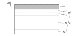
図1は、光学積層体の一実施形態である反射防止フィルムの積層構成例を示す断面図である。反射防止フィルム100は、ハードコートフィルム1のハードコート層11上に、反射防止層5を備える。反射防止層5は、屈折率の異なる2層以上の無機薄膜の積層体である。図1に示す反射防止フィルム100において、反射防止層5は、ハードコート層11と接する面に無機プライマー層50を備え、その上に高屈折率層51,53と低屈折率層52,54とが交互に積層されている。
FIG. 1 is a cross-sectional view showing an example of a laminated structure of an antireflection film, which is an embodiment of an optical laminate. The
以下では、図1に示す反射防止フィルムの好ましい形態に沿って、各層の材料や特性等ついて順に説明する。 Below, the materials and characteristics of each layer will be explained in order according to the preferred form of the antireflection film shown in FIG.
[ハードコートフィルム]
ハードコートフィルム1は、フィルム基材10の少なくとも一方の面にハードコート層11を備え、ハードコート層11上に無機薄膜5を設けることにより光学積層体が形成される。図2に示す様に、ハードコートフィルムは、フィルム基材10の両方の主面にハードコート層11,12を備えていてもよい。ハードコートフィルムが両面にハードコート層を備える場合は、一方のハードコート層11(前面ハードコート層)上に、無機薄膜5が設けられる。光学積層体は、ハードコートフィルムの両面に無機薄膜を備えていてもよい。
[Hard coat film]
The
<フィルム基材>
ハードコートフィルム1のフィルム基材10としては、透明フィルムが好ましく用いられる。透明フィルムの可視光透過率は、好ましくは80%以上、より好ましくは90%以上である。透明フィルムを構成する樹脂材料としては、透明性、機械強度、および熱安定性に優れる樹脂材料が好ましい。樹脂材料の具体例としては、トリアセチルセルロース等のセルロース系樹脂、ポリエステル系樹脂、ポリエーテルスルホン系樹脂、ポリスルホン系樹脂、ポリカーボネート系樹脂、ポリアミド系樹脂、ポリイミド系樹脂、ポリオレフィン系樹脂、(メタ)アクリル系樹脂、環状ポリオレフィン系樹脂(ノルボルネン系樹脂)、ポリアリレート系樹脂、ポリスチレン系樹脂、ポリビニルアルコール系樹脂、およびこれらの混合物が挙げられる。
<Film base material>
As the
フィルム基材10は必ずしも透明である必要はない。また、フィルム基材10として、複数のフィルムの積層体を用いてもよい。例えば、後述するように、偏光子の表面に保護フィルムが設けられた偏光板をフィルム基材10として用いてもよい。
The
フィルム基材の厚みは特に限定されないが、強度や取扱性等の作業性、薄層性等の観点から、5~300μm程度が好ましく、10~250μmがより好ましく、20~200μmがさらに好ましい。 The thickness of the film base material is not particularly limited, but from the viewpoint of workability such as strength and handleability, thin layer property, etc., it is preferably about 5 to 300 μm, more preferably 10 to 250 μm, and even more preferably 20 to 200 μm.
<前面ハードコート層>
フィルム基材10の主面上にハードコート層11を設けることによりハードコートフィルム1が形成される。硬度を高める観点から、ハードコート層11の厚み(積層構成である場合は合計厚み)は、7μm以上が好ましく、10μm以上がより好ましく、12μm以上がさらに好ましく、15μm以上、18μm以上または20μm以上であってもよい。硬度の観点からはハードコート層11の厚みの上限は特に制限されないが、ハードコート層の形成性や、透明性の観点からは50μm以下が好ましく、45μm以下がより好ましく、40μm以下がさらに好ましく、35μm以下または30μm以下であってもよい。
<Front hard coat layer>
一実施形態において、ハードコート層11は、2層以上のハードコート層の積層構成であり、最外表面(無機薄膜5形成面)の第一ハードコート層111、および第一ハードコート層111よりもフィルム基材10に近い側に配置された第二ハードコート層112を含む。例えば、フィルム基材10上に、第二ハードコート層112を形成し、その上に第一ハードコート層111を形成することにより、2層の積層構成を有するハードコート層が得られる。ハードコート層11は、3層以上を含んでいてもよい。2層以上の積層構成とすることにより、厚みが大きいハードコート層を容易に形成できる。
In one embodiment, the
(第一ハードコート層)
最表面の第一ハードコート層111は、無機微粒子を含む。第一ハードコート層111が無機微粒子を含むことにより、ハードコート層11の表面硬度が高められるとともに、表面に凹凸が形成され、ハードコート層11上に設けられる無機薄膜5との密着性を向上できる。
(first hard coat layer)
The first
無機微粒子の材料としては、シリカ、酸化チタン、酸化アルミニウム、酸化ジルコニウム、酸化チタン、酸化ニオブ、酸化亜鉛、酸化スズ、酸化セリウム、酸化マグネシウム、炭酸カルシウム、硫酸カルシウム、硫酸バリウム、タルク、カオリン等が挙げられる。これらの中でも、屈折率が低く、バインダー樹脂との屈折率差を小さくできることから、シリカ粒子が好ましい。無機微粒子として、多孔質粒子や中空粒子を用いてもよい。無機微粒子の表面には、樹脂との密着性や親和性を高める目的で、アクリル基、エポキシ基等の官能基が導入されていてもよい。 Materials for inorganic fine particles include silica, titanium oxide, aluminum oxide, zirconium oxide, titanium oxide, niobium oxide, zinc oxide, tin oxide, cerium oxide, magnesium oxide, calcium carbonate, calcium sulfate, barium sulfate, talc, kaolin, etc. Can be mentioned. Among these, silica particles are preferred because they have a low refractive index and can reduce the difference in refractive index with the binder resin. Porous particles or hollow particles may be used as the inorganic fine particles. A functional group such as an acrylic group or an epoxy group may be introduced into the surface of the inorganic fine particles for the purpose of increasing adhesion or affinity with the resin.
無機微粒子の形状は特に限定されないが、アスペクト比が1.5以下の(略)球形状であることが好ましい。無機微粒子のアスペクト比は、1.2以下がより好ましく、1.1以下がさらに好ましい。球形状の無機微粒子を用いることにより、ハードコート層11の表面に、無機薄膜との密着性に優れる凹凸形状が形成されやすくなる。
Although the shape of the inorganic fine particles is not particularly limited, it is preferably (substantially) spherical with an aspect ratio of 1.5 or less. The aspect ratio of the inorganic fine particles is more preferably 1.2 or less, and even more preferably 1.1 or less. By using spherical inorganic fine particles, the surface of the
無機薄膜5との密着性を向上に適した表面凹凸を形成する観点から、第一ハードコート層111に含まれる無機微粒子の平均一次粒子径D1は、好ましくは30~70nmであり、35~65nm、または40~60nmであってもよい。微粒子の一次粒子径は、コールター法により求められ、粒度分布における中央値D50を平均一次粒子径とする。
From the viewpoint of forming surface irregularities suitable for improving adhesion with the inorganic
微粒子での光散乱等に起因する反射光および透過光の色付きを抑制する観点から、第一ハードコート層111は、粗大な粒子の含有量が少ないことが好ましい。第一ハードコート層111に含まれる無機微粒子の90%粒子径(D90)は、100nm以下が好ましく、80nm以下がより好ましく、70nm以下がさらに好ましい。凝集を防止する観点から、無機微粒子の10%粒子径(D10)は、5nm以上が好ましく、10nm以上がより好ましく、15nm以上がさらに好ましい。コールターカウント法による累積粒度分布(重量基準)において、粒子径が小さい側から累積10%となる粒子径がD10であり、粒子径が小さい側から累積90%となる粒子径がD90である。例えば、D90が100nm以下の場合は、粒子径が100nm以上の粒子の量が重量基準で10%以下である。
From the viewpoint of suppressing coloring of reflected light and transmitted light due to light scattering by fine particles, it is preferable that the first
第一ハードコート層111は、無機微粒子に加えて有機微粒子を含んでいてもよいが、有機微粒子を含む場合も、第一ハードコート層111に含まれる微粒子全体のD90およびD10が上記範囲内であることが好ましい。無機薄膜5との密着性向上の観点から、第一ハードコート層111は、有機微粒子を含まないことが好ましく、有機微粒子を含む場合であっても、その含有量が無機微粒子の含有量よりも少ないことが好ましい。第一ハードコート層における有機微粒子の含有量(重量濃度)は、無機微粒子の含有量の50%以下が好ましく、30%以下がより好ましく、10%以下がさらに好ましく、5%以下、3%以下、1%以下または0であってもよい。
The first
第一ハードコート層111における無機微粒子の含有量は、固形分全量(バインダと微粒子の合計)に対して、20~80重量%が好ましい。無機微粒子の含有量が上記範囲内であれば、バインダー樹脂中への微粒子の分散性に優れ、凸部が面内に均一に分布した凹凸形状が形成されやすい。特に、ハードコート層の表面粗さを大きくして、ハードコート層と無機薄膜との密着性を高めるためには、第一ハードコート層における無機微粒子の含有量は、25~75重量%が好ましく、30~70重量%、35~65重量%または40~60重量%であってもよい。
The content of inorganic fine particles in the first
第一ハードコート層111は、厚み方向で微粒子含有量の分布を有していてもよく、表面(無機薄膜との界面)近傍の微粒子含有量が大きくてもよい。例えば、第一ハードコート層の形成時に表面に微粒子を偏在させることにより、表面近傍の微粒子含有量が相対的に大きいハードコート層が得られる。また、ハードコート層を形成後(バインダーを硬化後)に、プラズマ処理等のドライエッチングやウェットエッチングにより、表面近傍のバインダーを選択的にエッチングすることにより、表面近傍の微粒子含有量が相対的に大きいハードコート層が得られる。
The first
ハードコート層11は、表面(無機薄膜との界面)から厚み方向に1μmの範囲における無機微粒子の含有量が、20重量%以上であることが好ましく、30重量%以上がより好ましく、40重量%以上がさらに好ましく、50重量%以上、60重量%以上、70重量%以上、75重量%以上または80重量%以上であってもよい。無機薄膜5との界面近傍の無機微粒子の存在比を高めることにより、ハードコート層11の表面において、微粒子が表面に露出している面積の比率が高くなり、無機薄膜との密着性が向上する傾向がある。
In the
ハードコート層の表面近傍の微粒子の含有量が過度に大きい場合は、粒子が脱落しやすく、ハードコート層11の表面の凹凸形状が不均一となる場合がある。そのため、ハードコート層11の表面から厚み方向に1μmの範囲における無機微粒子の含有量は、97重量%以下が好ましく、95重量%以下がより好ましく、93重量%以下または90重量%以下であってもよい。
If the content of fine particles near the surface of the hard coat layer is excessively large, the particles tend to fall off, and the surface of the
無機薄膜との密着性を確保しつつ、微粒子の脱落等を抑制する観点から、ハードコート層11の断面において、表面(無機薄膜との界面)から厚み方向に1μmの範囲における無機微粒子が占める面積比率は、20~97%が好ましく、30~95%がより好ましく、40%以上、50%以上、60%以上、70%以上、75%以上または80%以上であってもよく、93%以下または90%以下であってもよい。
In order to ensure adhesion with the inorganic thin film and suppress the falling off of the fine particles, the area occupied by the inorganic fine particles in the cross section of the
ハードコート層の断面において無機微粒子が占める面積比率は、断面の電子顕微鏡観察により得られた観察像(断面像)を二値化処理して、微粒子が占める領域を特定し、その面積比率を算出することにより求められる。 The area ratio occupied by inorganic fine particles in the cross section of the hard coat layer can be determined by binarizing the observed image (cross-sectional image) obtained by electron microscopic observation of the cross section, identifying the area occupied by the fine particles, and calculating the area ratio. It is determined by
無機薄膜との密着性向上の観点から、ハードコート層11の表面(無機薄膜形成面)の算術平均高さSaは、1.0nm以上が好ましく、1.5nm以上がより好ましく、2.0nm以上がさらに好ましく、2.5nm以上、3.0nm以上、3.5nm以上、4.0nm以上または4.5nm以上であってもよい。一方、ハードコート層の表面凹凸が粗大になると、十分な密着性を実現できない場合がある。そのため、ハードコート層11の表面の算術平均高さSaは、8nm以下が好ましく、7.5nm以下がより好ましく、7nm以下がさらに好ましく、6nm以下または5.5nm以下であってもよい。算術平均高さSaは、原子間力顕微鏡(AFM)を用いた1μm四方の観察像から、ISO 25178に準じて算出される。
From the viewpoint of improving adhesion with the inorganic thin film, the arithmetic mean height Sa of the surface of the hard coat layer 11 (inorganic thin film forming surface) is preferably 1.0 nm or more, more preferably 1.5 nm or more, and 2.0 nm or more. is more preferable, and may be 2.5 nm or more, 3.0 nm or more, 3.5 nm or more, 4.0 nm or more, or 4.5 nm or more. On the other hand, if the surface irregularities of the hard coat layer become coarse, sufficient adhesion may not be achieved. Therefore, the arithmetic mean height Sa of the surface of the
上記の様に、第一ハードコート層111が無機微粒子を含むことにより表面凹凸が形成され、無機微粒子の粒子径および含有量を調整することにより、上記のSaを有するハードコート層11が得られる。また、微粒子を含むハードコート層をドライエッチングまたはウェットエッチングして、微粒子を表面に露出させることにより、ハードコート層11の算術平均高さSaを大きくすることもできる。
As described above, surface irregularities are formed by the first
(第二ハードコート層)
ハードコート層11は、第一ハードコート層111よりもフィルム基材10に近い側に配置された第二ハードコート層112を備える。
(Second hard coat layer)
The
上記の様に、ハードコート層11の最表面の第一ハードコート層が、平均一次粒子径D1が30~70nmである無機微粒子を含むことにより、ハードコート層11上に形成される無機薄膜5との密着性が高められる。一方、ハードコート層の硬度向上等を目的として、平均一次粒子径が30nm以上の微粒子を含むハードコート層の厚みを大きくすると、ハードコート層の耐屈曲性が低下し、ロール搬送時や他の部材との貼り合わせ等のハンドリング時にハードコート層に割れやクラックが生じやすく、ハンドリング性が低下する傾向がある。
As described above, since the first hard coat layer on the outermost surface of the
第一ハードコート層111よりもフィルム基材10に近い側に、第一ハードコート層の微粒子よりも粒子径が小さい無機粒子を含むか、または第一ハードコート層よりも無機微粒子の含有量が少ない(または無機微粒子を含まない)第二ハードコート層112を設け、ハードコート層11を多層構成とすることにより、第一ハードコート層111による無機薄膜との密着性を維持したまま、ハードコート層全体の厚みを大きくして硬度を高めつつ、ハードコート層11の耐屈曲性が向上する傾向がある。
The side closer to the
(第二ハードコート層の第1形態)
1つの実施形態では、第二ハードコート層112が無機微粒子を含み、その平均一次粒子径D2が、第一ハードコート層111の無機微粒子の平均一次粒子径D1よりも小さい。D2がD1よりも小さいことにより、ハードコート層11全体に含まれる無機微粒子の平均一次粒子径Dが、D1よりも小さいため、ハードコート層11の耐屈曲性が向上する傾向がある。換言すると、第一ハードコート層111の無機微粒子の平均一次粒子径D1が、ハードコート層全体に含まれる無機微粒子の平均一次粒子径Dよりも大きいことにより、ハードコート層11の耐屈曲性を低下させることなく、無機薄膜5との密着性を向上できる。
(First form of second hard coat layer)
In one embodiment, the second
ハードコート層の耐屈曲性を向上して、割れやクラックの発生を抑制する観点から、第二ハードコート層112に含まれる無機微粒子の平均一次粒子径D2は、30nm未満が好ましく、28nm以下がより好ましく、25nm以下または20nm以下であってもよい。無機微粒子の分散性を確保する観点から、D2は5nm以上が好ましく、10nm以上であってもよい。ハードコート層11全体に含まれる無機微粒子の平均一次粒子径Dは、10~70nmが好ましく、15~60nmがより好ましく、20~55nm、または23~50nmであってもよい。
From the viewpoint of improving the flex resistance of the hard coat layer and suppressing the occurrence of breakage or cracking, the average primary particle diameter D2 of the inorganic fine particles contained in the second
ハードコート層の割れやクラックを防止する観点から、第二ハードコート層112は、粗大な粒子の含有量が少ないことが好ましい。第二ハードコート層112に含まれる無機微粒子の90%粒子径(D90)は、60nm以下が好ましく、40nm以下がより好ましく、30nm以下がさらに好ましい。凝集を防止する観点から、無機微粒子の10%粒子径(D10)は、3nm以上が好ましく、5nm以上がより好ましい。
From the viewpoint of preventing cracks in the hard coat layer, it is preferable that the second
第二ハードコート層112は、無機微粒子に加えて有機微粒子を含んでいてもよいが、有機微粒子を含む場合も、第二ハードコート層112に含まれる微粒子全体のD90およびD10が上記範囲内であることが好ましい。無機薄膜5との密着性向上の観点から、第二ハードコート層112は、有機微粒子を含まないことが好ましく、有機微粒子を含む場合であっても、その含有量が無機微粒子の含有量よりも少ないことが好ましい。第二ハードコート層における有機微粒子の含有量(重量濃度)は、無機微粒子の含有量の50%以下が好ましく、30%以下がより好ましく、10%以下がさらに好ましく、5%以下、3%以下、1%以下または0であってもよい。
The second
第二ハードコート層に含まれる無機微粒子の材料および形状の好ましい形態は、第一ハードコート層の無機微粒子について前述したものと同様である。 The preferred material and shape of the inorganic fine particles included in the second hard coat layer are the same as those described above for the inorganic fine particles in the first hard coat layer.
ハードコート層の耐屈曲性向上の観点から、第二ハードコート層112における無機微粒子の含有量は、固形分全量(バインダと微粒子の合計)に対して、80重量%以下が好ましく、70重量%以下がより好ましく、60重量%以下がさらに好ましく、50重量%以下または40重量%以下であってもよい。
From the viewpoint of improving the bending resistance of the hard coat layer, the content of inorganic fine particles in the second
後述のように、第二ハードコート層112は無機微粒子を含まないものであってもよい。ハードコート層11の硬度を高める観点においては、第二ハードコート層112は無機微粒子を含むことが好ましく、第二ハードコート層112における無機微粒子の含有量は、固形分全量に対して5重量%以上が好ましく、10重量%以上がより好ましく、15重量%以上、20重量%以上または25重量%以上であってもよい。
As described later, the second
第二ハードコート層112の無機微粒子の重量濃度は、第一ハードコート層111の無機微粒子の重量濃度と同じでもよく、第一ハードコート層111の無機微粒子の重量濃度よりも大きくてもよく、第一ハードコート層111の無機微粒子の重量濃度よりも小さくてもよい。
The weight concentration of the inorganic fine particles in the second
(第二ハードコート層の第2形態)
1つの実施形態では、第二ハードコート層112の無機微粒子の重量濃度が、第一ハードコート層111の無機微粒子の重量濃度よりも小さく、第二ハードコート層112は微粒子を含まないものであってもよい。第二ハードコート層の微粒子濃度が小さいことにより、ハードコート層の全体(バルク)の微粒子濃度が、第一ハードコート層の微粒子の濃度よりも小さくなり、ハードコート層の耐屈曲性が向上する場合がある。換言すると、第一ハードコート層111の無機微粒子の重量濃度が、ハードコート層11全体の無機微粒子の重量濃度よりも大きいことにより、ハードコート層11の耐屈曲性を低下させることなく、無機薄膜5との密着性を向上できる。第二ハードコート層112の無機微粒子の重量濃度は、第一ハードコート層111の無機微粒子の重量濃度の0.9倍以下、0.8倍以下、0.7倍以下、0.6倍以下、0.5倍以下、0.4倍以下、0.3倍以下または0.2倍以下であってもよく、第二ハードコート層112は無機微粒子を含まないものであってもよい。
(Second form of second hard coat layer)
In one embodiment, the weight concentration of the inorganic fine particles in the second
第二ハードコート層が無機微粒子を含む場合、その平均一次粒子径D2は、第一ハードコート層111の無機微粒子の平均一次粒子径D1と同じでもよく、D1よりも大きくてもよく、D1よりも小さくてもよい。ハードコート層の割れやクラックの発生を抑制する観点から、上記の第1形態と同様、D2は、D1よりも小さいことが好ましく、30nm未満が好ましく、28nm以下がより好ましく、25nm以下または20nm以下であってもよい。無機微粒子の分散性を確保する観点から、D2は5nm以上が好ましく、10nm以上であってもよい。
When the second hard coat layer contains inorganic fine particles, the average primary particle diameter D2 thereof may be the same as the average primary particle diameter D1 of the inorganic fine particles of the first
第2形態において、第二ハードコート層112の無機微粒子の種類、粒子径の分布、および含有量(重量濃度)の好ましい範囲は、第1形態について上述したものと同様である。
In the second embodiment, the preferred ranges of the type, particle size distribution, and content (weight concentration) of the inorganic fine particles in the second
(ハードコート層の形成)
バインダー樹脂成分(バインダー樹脂を形成するための硬化性樹脂成分)および無機微粒子を含むハードコート層形成用組成物を、フィルム基材上に塗布し、バインダー樹脂成分を硬化することによりハードコート層11が形成される。フィルム基材10上に、第二ハードコート層112を形成した後、第二ハードコート層112上に第一ハードコート層111を形成することにより、フィルム基材10上に、第二ハードコート層112および第一ハードコート層111を順に備えるハードコートフィルム1が得られる。
(Formation of hard coat layer)
A
多層ダイ等を用いて、2層以上のハードコート層を同時に形成してもよい。第二ハードコート層の形成前、および/または第二ハードコート層を形成後第一ハードコート層の形成前に、他のハードコート層を形成して、3層以上の積層構成を有するハードコート層を形成してもよい。 Two or more hard coat layers may be formed simultaneously using a multilayer die or the like. A hard coat having a laminated structure of three or more layers by forming another hard coat layer before forming the second hard coat layer and/or after forming the second hard coat layer and before forming the first hard coat layer. A layer may be formed.
ハードコート層のバインダー樹脂としては、熱硬化性樹脂、光硬化性樹脂、電子線硬化性樹脂等の硬化性樹脂が好ましく用いられる。硬化性樹脂の種類としてはポリエステル系、アクリル系、ウレタン系、アクリルウレタン系、アミド系、シリコーン系、シリケート系、エポキシ系、メラミン系、オキセタン系、アクリルウレタン系等が挙げられる。これらの中でも、硬度が高く、光硬化が可能であることから、アクリル系樹脂、アクリルウレタン系樹脂、およびエポキシ系樹脂が好ましい。 As the binder resin for the hard coat layer, curable resins such as thermosetting resins, photocurable resins, and electron beam curable resins are preferably used. Examples of the curable resin include polyester, acrylic, urethane, acrylic urethane, amide, silicone, silicate, epoxy, melamine, oxetane, and acrylic urethane. Among these, acrylic resins, acrylic urethane resins, and epoxy resins are preferred because they have high hardness and can be photocured.
光硬化性のバインダー樹脂成分は、2個以上の光重合性(好ましくは紫外線重合性)の官能基を有する多官能化合物を含む。多官能化合物はモノマーでもオリゴマーでもよい。光重合性の多官能化合物としては、1分子中に2個以上の(メタ)アクリロイル基を含む化合物が好ましく用いられる。 The photocurable binder resin component includes a polyfunctional compound having two or more photopolymerizable (preferably ultraviolet polymerizable) functional groups. The polyfunctional compound may be a monomer or an oligomer. As the photopolymerizable polyfunctional compound, a compound containing two or more (meth)acryloyl groups in one molecule is preferably used.
第一ハードコート層のバインダー樹脂の組成と第二ハードコート層のバインダー樹脂の組成は同一でもよく異なっていてもよい。 The composition of the binder resin of the first hard coat layer and the composition of the binder resin of the second hard coat layer may be the same or different.
ハードコート層形成用組成物は、上記のバインダー樹脂成分および無機微粒子を含み、必要に応じてバインダー樹脂成分を溶解可能な溶媒を含む。第二ハードコート層が無機微粒子を含まない場合は、第二ハードコート層形成用の組成物には無機微粒子を含める必要はない。 The composition for forming a hard coat layer contains the above binder resin component and inorganic fine particles, and optionally contains a solvent capable of dissolving the binder resin component. When the second hard coat layer does not contain inorganic fine particles, the composition for forming the second hard coat layer does not need to contain inorganic fine particles.
バインダー樹脂成分が硬化性樹脂である場合は、組成物中に、適宜の重合開始剤が含まれていることが好ましい。例えば、バインダー樹脂成分が光硬化型樹脂である場合には、組成物中に光重合開始剤が含まれることが好ましい。ハードコート層形成用組成物は、上記の他に、レベリング剤、チクソトロピー剤、帯電防止剤、ブロッキング防止剤、分散剤、分散安定剤、酸化防止剤、紫外線吸収剤、消泡剤、増粘剤、界面活性剤、滑剤等の添加剤を含んでいてもよい。 When the binder resin component is a curable resin, it is preferable that an appropriate polymerization initiator is included in the composition. For example, when the binder resin component is a photocurable resin, it is preferable that a photopolymerization initiator is included in the composition. In addition to the above, the composition for forming a hard coat layer also contains a leveling agent, a thixotropic agent, an antistatic agent, an antiblocking agent, a dispersant, a dispersion stabilizer, an antioxidant, an ultraviolet absorber, an antifoaming agent, and a thickening agent. , a surfactant, a lubricant, and other additives.
フィルム基材上にハードコート層形成用組成物を塗布し、必要に応じて溶媒の除去および樹脂の硬化を行うことにより、ハードコート層が形成される。ハードコート層形成用組成物の塗布方法としては、バーコート法、ロールコート法、グラビアコート法、ロッドコート法、スロットオリフィスコート法、カーテンコート法、ファウンテンコート法、コンマコート法等の任意の適切な方法を採用し得る。上記の様に、多層ダイ等を用いて、フィルム基材上に2層以上を同時に塗布してもよい。 A hard coat layer is formed by applying a composition for forming a hard coat layer onto a film base material, and removing the solvent and curing the resin as necessary. The hard coat layer forming composition can be applied by any suitable method such as bar coating, roll coating, gravure coating, rod coating, slot orifice coating, curtain coating, fountain coating, comma coating, etc. method can be adopted. As mentioned above, two or more layers may be applied simultaneously onto a film substrate using a multilayer die or the like.
塗布後の加熱温度は、ハードコート層形成用組成物の組成等に応じて、適切な温度に設定すればよく、例えば、50℃~150℃程度である。バインダー樹脂成分が光硬化性樹脂である場合は、紫外線等の活性エネルギー線を照射することにより光硬化が行われる。照射光の積算光量は、好ましくは100~500mJ/cm2程度である。 The heating temperature after coating may be set to an appropriate temperature depending on the composition of the composition for forming a hard coat layer, and is, for example, about 50°C to 150°C. When the binder resin component is a photocurable resin, photocuring is performed by irradiation with active energy rays such as ultraviolet rays. The cumulative amount of irradiation light is preferably about 100 to 500 mJ/cm 2 .
第二ハードコート層と第一ハードコート層を順に製膜する場合は、第二ハードコート層の硬化前に第一ハードコート層を塗布してもよく、第二ハードコート層を硬化後に第一ハードコート層を塗布してもよい。第二ハードコート層を塗布し、溶媒を除去後に第一ハードコート層の塗布および溶媒の除去を行い、第二ハードコート層の硬化と第一ハードコート層の硬化を同時に実施してもよい。 When forming the second hard coat layer and the first hard coat layer in order, the first hard coat layer may be applied before the second hard coat layer is cured, and the first hard coat layer may be applied after the second hard coat layer is cured. A hard coat layer may also be applied. After applying the second hard coat layer and removing the solvent, the first hard coat layer may be applied and the solvent removed, and the second hard coat layer and the first hard coat layer may be cured simultaneously.
ハードコート層11上に無機薄膜5を形成する前に、ハードコート層11の表面(第一ハードコート層111の表面)の表面処理を行ってもよい。表面処理としては、コロナ処理、プラズマ処理、フレーム処理、オゾン処理、プライマー処理、グロー処理、アルカリ処理、酸処理、カップリング剤による処理等の表面改質処理が挙げられる。表面処理として真空プラズマ処理を行ってもよい。
Before forming the inorganic
表面処理によりハードコート層をエッチングして、ハードコート層11の表面粗さを調整することもできる。例えば、高放電電力で真空プラズマ処理を行えば、ハードコート層表面の樹脂成分が選択的にエッチングされやすく、無機微粒子はほとんどエッチングされずに残存するため、ハードコート層表面およびその近傍における無機微粒子の存在比率が高くなり、ハードコート層表面の算術平均高さSaが大きくなる傾向がある。
The surface roughness of the
真空プラズマ処理における雰囲気ガスとしては、ヘリウム、ネオン、アルゴン、クリプトン、キセノン、ラドン等の不活性ガスが好ましく、中でもアルゴンが好ましい。真空プラズマ処理における放電電力は、例えば、0.08~4kW程度である。放電電力が過度に高いと、バインダー樹脂のエッチングが過度に進行して、ハードコート層表面の凹凸の粗大化や、無機微粒子の脱落が生じやすく、密着性の低下を招く場合がある。放電電力が過度に低いと、放電が不安定になり処理面の均一性の低下を招く場合がある。そのため、真空プラズマ処理における放電電力は、1kW以下が好ましく、0.5kW以下がより好ましい。処理時間は、0.05~1.0秒程度が好ましく、0.1~0.6秒がより好ましい。放電時のエネルギー密度は、0.1~5.0kW/m2程度が好ましく、0.15~2.0kW/m2がより好ましい。 As the atmospheric gas in the vacuum plasma treatment, inert gases such as helium, neon, argon, krypton, xenon, and radon are preferred, and argon is especially preferred. The discharge power in vacuum plasma processing is, for example, about 0.08 to 4 kW. If the discharge power is too high, the etching of the binder resin will proceed excessively, and the roughness of the surface of the hard coat layer will become coarse, and inorganic fine particles will easily fall off, which may lead to a decrease in adhesion. If the discharge power is too low, the discharge may become unstable and the uniformity of the treated surface may deteriorate. Therefore, the discharge power in the vacuum plasma treatment is preferably 1 kW or less, more preferably 0.5 kW or less. The processing time is preferably about 0.05 to 1.0 seconds, more preferably 0.1 to 0.6 seconds. The energy density during discharge is preferably about 0.1 to 5.0 kW/m 2 , more preferably 0.15 to 2.0 kW/m 2 .
(ハードコート層の厚み)
前述のように、ハードコート層11の厚みは、好ましくは7~50μmである。ハードコート層11が第一ハードコート層111と第二ハードコート層112の2層構成の場合は、第一ハードコート層111の厚みと第二ハードコート層112の厚みの合計が上記範囲であることが好ましい。
(Thickness of hard coat layer)
As mentioned above, the thickness of the
ハードコート層11上に無機薄膜5を備える光学積層体の硬度は、ハードコート層11の最表面層であり、無機薄膜5の下地である、第一ハードコート層111の影響が大きい。平均一次粒子径D1が30~70nmの無機微粒子を含む第一ハードコート層111の厚みが大きいほど、硬度が高くなる傾向がある。そのため、第一ハードコート層111の厚みは、1μm以上が好ましく、2μm以上がより好ましく、2.5μm以上、3μm以上、4μm以上または5μm以上であってもよい。一方、第一ハードコート層111の厚みが過度に大きいと、ハードコート層の耐屈曲性の低下や、表面形状の平滑化(Saの減少)に伴う無機薄膜の密着性低下の原因となる場合がある。そのため、第一ハードコート層111の厚みは、15μm以下が好ましく、12μm以下がより好ましく、10μm以下または8μm以下であってもよい。
The hardness of the optical laminate including the inorganic
ハードコート層の耐屈曲性を高めるためには、第一ハードコート層111は、無機薄膜との密着性および表面硬度を確保可能な範囲で、できる限り厚みが小さいことが好ましい。第一ハードコート層111の厚みは、ハードコート層11の全体の厚みの50%以下が好ましく、40%以下、30%以下または25%以下であってもよい。硬度向上の観点から、第一ハードコート層111の厚みは、ハードコート層11の全体の厚みの5%以上が好ましく、10%以上がより好ましく、15%以上または20%以上であってもよい。
In order to improve the bending resistance of the hard coat layer, the thickness of the first
ハードコート層11の耐屈曲性を向上しつつ、硬度を高める観点から、第二ハードコート層112の厚みは、5μm以上が好ましく、8μm以上がより好ましく、10μm以上、12μm以上または14μm以上であってもよい。ハードコート層の厚みの均一化および耐屈曲性向上の観点から、第二ハードコート層112の厚みは、30μm以下が好ましく、25μm以下がより好ましく、22μm以下または20μm以下であってもよい。
From the viewpoint of increasing the hardness while improving the bending resistance of the
ハードコート層の耐屈曲性を高めるためには、第一ハードコート層111の厚みは第二ハードコート層112の厚みよりも小さいことが好ましい。第一ハードコート層111の厚みは、第二ハードコート層112の厚みの0.9倍以下、0.8倍以下、0.7倍以下、0.6倍以下、0.5倍以下、0.4倍以下または0.3倍以下であってもよい。硬度向上の観点から、第一ハードコート層111の厚みは、第二ハードコート層112の厚みの0.1倍以上が好ましく、0.15倍以上、0.2倍以上または0.25倍以上であってもよい。
In order to improve the bending resistance of the hard coat layer, the thickness of the first
(ハードコート層の微粒子の分布)
本発明においては、ハードコート層11の無機薄膜5との界面近傍に、粒子径が30~70nm程度である無機微粒子が相対的に多く存在することにより、ハードコート層11の耐屈曲性を維持しつつ、表面硬度および無機薄膜との密着性を向上できる。
(Distribution of fine particles in hard coat layer)
In the present invention , the bending resistance of the
ハードコート層11の表面(無機薄膜5との界面)から厚み方向に1μmの範囲における無機微粒子の平均一次粒子径Daは、30~70nmが好ましく、35~65nm、または40~60nmであってもよい。ハードコート層11全体に含まれる無機微粒子の平均一次粒子径Dは、Daよりも小さいことが好ましい。
The average primary particle diameter Da of the inorganic fine particles in the range of 1 μm in the thickness direction from the surface of the hard coat layer 11 (interface with the inorganic thin film 5) is preferably 30 to 70 nm, even if it is 35 to 65 nm, or 40 to 60 nm. good. The average primary particle diameter D of the inorganic fine particles contained in the entire
前述の通り、ハードコート層11の表面から厚み方向に1μmの範囲における無機微粒子の含有量(重量濃度)は、20重量%以上が好ましく、30~97重量%より好ましく、40重量~96重量%がさらに好ましく、50重量%以上、60重量%以上、70重量%以上、75重量%以上または80重量%以上であってもよく、95重量%以下、93重量%以下または90重量%以下であってもよい。ハードコート層11の表面から厚み方向に1μmの範囲における無機微粒子の重量濃度は、ハードコート層11全体の無機微粒子の重量濃度よりも大きくてもよい。ハードコート層11において、無機微粒子は、表面(無機薄膜5との界面)近傍に偏在していてもよい。
As mentioned above, the content (weight concentration) of inorganic fine particles in the range of 1 μm from the surface of the
ハードコート層11の断面において、表面から厚み方向に1μmの範囲における無機微粒子が占める面積比率は、20~97%が好ましく、30~95%がより好ましく、40%以上、50%以上、60%以上、70%以上、75%以上または80%以上であってもよく、93%以下または90%以下であってもよい。
In the cross section of the
<裏面ハードコート層>
前述のように、ハードコートフィルムは、フィルム基材10の一方の主面(無機薄膜5形成面)に前面ハードコート層11を備え、フィルム基材10の他方の面に裏面ハードコート層12を備えていてもよい。裏面ハードコート層12が設けられることにより、光学積層体全体の硬度が高められ、無機薄膜5側の表面硬度が向上する場合がある。
<Back hard coat layer>
As described above, the hard coat film includes the front
裏面ハードコート層12の組成は特に限定されず、微粒子を含んでいてもよく含んでいなくてもよい。裏面ハードコート層12は単層でもよく、2層以上の積層構成でもよい。硬度向上の観点から、裏面ハードコート層12の厚みは、1μm以上が好ましく、2μm以上がより好ましく、3μm以上、4μm以上または5μm以上であってもよい。
The composition of the back
裏面ハードコート層12の厚みは、40μm以下、30μm以下または20μm以下であってもよい。裏面ハードコート層12の厚みは、前面ハードコート層11の厚みよりも小さくてもよい。裏面ハードコート層の厚みは、前面ハードコート層11の厚みの0.9倍以下、0.8倍以下、0.7倍以下、0.6倍以下、0.5倍以下、0.4倍以下、または0.3倍以下であってもよい。表面硬度向上の観点から、裏面ハードコート層12が設けられる場合、その厚みは、前面ハードコート層11の厚みの0.1倍以上が好ましく、0.2倍以上または0.25倍以上であってもよい。
The thickness of the back
[無機薄膜]
ハードコートフィルム1のハードコート層11上に無機薄膜5を形成することにより、光学積層体が得られる。無機薄膜の材料としては、金属や金属化合物(金属または半金属の酸化物、窒化物、炭化物、硫化物、フッ化物等)等が挙げられる。無機薄膜は、導電性でも絶縁性でもよく、半導体でもよい。ハードコート層上に無機薄膜が設けられることにより、各種の機能が付与される。例えば、図1に示すように、無機薄膜として屈折率の異なる複数の薄膜を積層することにより、反射防止層が形成され、ハードコート付き反射防止フィルムが得られる。無機薄膜5の膜厚(複数の薄膜を含む場合は合計膜厚)は、例えば1nm~1μm程度であり、薄膜の種類や光学積層体の機能等に応じて、適宜に調整すればよい。
[Inorganic thin film]
By forming the inorganic
<反射防止層>
以下では、無機薄膜として、屈折率の異なる複数の薄膜からなる反射防止層を形成する実施形態について説明する。
<Anti-reflection layer>
Below, an embodiment will be described in which an antireflection layer consisting of a plurality of thin films having different refractive indexes is formed as an inorganic thin film.
一般に、反射防止層は、入射光と反射光の逆転した位相が互いに打ち消し合うように、薄膜の光学膜厚(屈折率と厚みの積)が調整される。屈折率の異なる複数の薄膜の多層積層体により、可視光の広帯域の波長範囲において、反射率を小さくできる。反射防止層5を構成する薄膜の材料としては、金属の酸化物、窒化物、フッ化物等の無機材料が挙げられる。反射防止層5は、好ましくは、高屈折率層と低屈折率層の交互積層体である。空気界面での反射を低減するために、反射防止層5の最外層(ハードコートフィルム1から最も離れた層)として設けられる薄膜54は、低屈折率層であることが好ましい。
Generally, the optical thickness (product of refractive index and thickness) of the thin film of the antireflection layer is adjusted so that the reversed phases of incident light and reflected light cancel each other out. By using a multilayer stack of a plurality of thin films having different refractive indexes, it is possible to reduce the reflectance in a wide wavelength range of visible light. Examples of the material of the thin film constituting the
高屈折率層51,53は、例えば屈折率が1.9以上、好ましくは2.0以上である。高屈折率材料としては、酸化チタン、酸化ニオブ、酸化ジルコニウム、酸化タンタル、酸化亜鉛、酸化インジウム、酸化インジウムスズ(ITO)、アンチモンドープ酸化スズ(ATO)等が挙げられる。中でも、酸化チタンまたは酸化ニオブが好ましい。低屈折率層52,54は、例えば屈折率が1.6以下、好ましくは1.5以下である。低屈折率材料としては、酸化シリコン、窒化チタン、フッ化マグネシウム、フッ化バリウム、フッ化カルシウム、フッ化ハフニウム、フッ化ランタン等が挙げられる。中でも酸化シリコンが好ましい。特に、高屈折率層としての酸化ニオブ(Nb2O5)薄膜51,53と、低屈折率層としての酸化シリコン(SiO2)薄膜52,54とを交互に積層することが好ましい。低屈折率層と高屈折率層に加えて、屈折率1.6~1.9程度の中屈折率層が設けられてもよい。
The high refractive index layers 51 and 53 have a refractive index of, for example, 1.9 or more, preferably 2.0 or more. Examples of the high refractive index material include titanium oxide, niobium oxide, zirconium oxide, tantalum oxide, zinc oxide, indium oxide, indium tin oxide (ITO), and antimony-doped tin oxide (ATO). Among these, titanium oxide or niobium oxide is preferred. The low refractive index layers 52 and 54 have a refractive index of, for example, 1.6 or less, preferably 1.5 or less. Examples of the low refractive index material include silicon oxide, titanium nitride, magnesium fluoride, barium fluoride, calcium fluoride, hafnium fluoride, and lanthanum fluoride. Among them, silicon oxide is preferred. In particular, it is preferable to alternately laminate niobium oxide (Nb 2 O 5 )
高屈折率層および低屈折率層の膜厚は、それぞれ、5~200nm程度であり、15~150nm程度が好ましい。屈折率や積層構成等に応じて、可視光の反射率が小さくなるように、各層の膜厚を設計すればよい。例えば、高屈折率層と低屈折率層の積層構成としては、ハードコートフィルム1側から、光学膜厚25nm~55nm程度の高屈折率層51、光学膜厚35nm~55nm程度の低屈折率層52、光学膜厚80nm~240nm程度の高屈折率層53、および光学膜厚120nm~150nm程度の低屈折率層54の4層構成が挙げられる。
The film thicknesses of the high refractive index layer and the low refractive index layer are each about 5 to 200 nm, preferably about 15 to 150 nm. The film thickness of each layer may be designed in accordance with the refractive index, laminated structure, etc. so that the reflectance of visible light is small. For example, the laminated structure of a high refractive index layer and a low refractive index layer includes, from the
反射防止層5は、好ましくは、ハードコートフィルム1のハードコート層11と接する面に無機プライマー層50を備え、その上に、高屈折率層および低屈折率層を備える。無機微粒子による表面凹凸が形成されたハードコート層11に接して無機プライマー層50を設け、無機プライマー層50上に接して高屈折率層や低屈折率層等の無機薄膜を設けることにより、層間の密着性に優れ、紫外線等の光に長時間晒された場合でも無機薄膜の剥離が生じ難い光学積層体(反射防止フィルム)が得られる。
The
プライマー層50を構成する無機材料としては、例えば、シリコン、ニッケル、クロム、スズ、インジウム、金、銀、白金、亜鉛、チタン、タングステン、アルミニウム、ジルコニウム、パラジウム等の金属;これらの金属の合金;これらの金属の酸化物、フッ化物、硫化物または窒化物;等の無機材料が挙げられる。中でも、プライマー層の無機材料は酸化物が好ましく、中でも、Si,In,Sn,Zn,Ti等の金属を含むものが好ましい。プライマー層50は、化学量論組成よりも酸素量が少ない無機酸化物層であってもよい。
Examples of inorganic materials constituting the
無機プライマー層50の厚みは、例えば、1~20nm程度であり、好ましくは2~15nm、より好ましくは3~10nmである。無機プライマー層の膜厚が上記範囲であれば、ハードコート層11との密着性と高い光透過性とを両立できる。
The thickness of the
反射防止層5を構成する薄膜の成膜方法は特に限定されず、ウェットコーティング法、ドライコーティング法のいずれでもよい。膜厚が均一な薄膜を形成できることから、真空蒸着、CVD,スパッタ、電子線蒸等のドライコーティング法が好ましい。中でも、膜厚の均一性に優れ、かつ緻密な膜を形成しやすいことから、スパッタ法が好ましい。
The method for forming the thin film constituting the
スパッタ法では、ロールトゥーロール方式により、長尺のハードコートフィルムを一方向(長手方向)に搬送しながら、薄膜を連続成膜できる。そのため、ハードコートフィルム上に無機薄膜を備える光学積層体無機薄膜フィルムの生産性を向上できる。特に、ハードコート層上に、反射防止層等の複数の薄膜を形成する場合は、フィルム搬送方向に沿って複数のターゲットを配置することにより、複数の薄膜を連続成膜可能であるため、ロールトゥーロールスパッタにより無機薄膜を成膜することが好ましい。反射防止フィルムの生産性を向上するためには、反射防止層5を構成する全ての薄膜をスパッタ法により成膜することが好ましい。
The sputtering method uses a roll-to-roll method to continuously form thin films while conveying a long hard coat film in one direction (longitudinal direction). Therefore, the productivity of the optical laminate inorganic thin film including the inorganic thin film on the hard coat film can be improved. In particular, when forming multiple thin films such as an antireflection layer on a hard coat layer, it is possible to continuously form multiple thin films by arranging multiple targets along the film transport direction. Preferably, the inorganic thin film is formed by two-roll sputtering. In order to improve the productivity of the antireflection film, it is preferable to form all the thin films constituting the
スパッタ法では、アルゴン等の不活性ガス、および必要に応じて酸素等の反応性ガスをチャンバー内に導入しながら成膜が行われる。スパッタ法による酸化物層の成膜は、酸化物ターゲットを用いる方法、および金属ターゲットを用いた反応性スパッタのいずれでも実施できる。高レートで金属酸化物を成膜するためには、金属ターゲットを用いた反応性スパッタが好ましい。 In the sputtering method, deposition is performed while introducing an inert gas such as argon, and if necessary, a reactive gas such as oxygen, into the chamber. Deposition of an oxide layer by sputtering can be performed either by using an oxide target, or by reactive sputtering using a metal target. To deposit a metal oxide film at a high rate, reactive sputtering using a metal target is preferred.
無機薄膜5の表面(ハードコート層11と反対側の面)の算術平均高さSaは、1.0nm以上が好ましく、1.5nm以上がより好ましく、2.0nm以上がさらに好ましく、2.5nm以上、3.0nm以上、3.5nm以上、4.0nm以上または4.5nm以上であってもよい。スパッタ法等のドライプロセスにより無機薄膜5を成膜すると、無機薄膜5の表面には、下地となるハードコート層11の表面形状を反映した凹凸形状が形成されやすい。前述のように、ハードコート層11(第一ハードコート層111)が無機微粒子を含み、表面に凹凸が形成されているため、無機薄膜5も、ハードコート層11の無機微粒子による凹凸形状を反映した表面形状が形成されやすい。無機薄膜5の表面の算術平均高さSaは、8nm以下が好ましく、7.5nm以下がより好ましく、7nm以下がさらに好ましく、6nm以下または5.5nm以下であってもよい。
The arithmetic mean height Sa of the surface of the inorganic thin film 5 (the surface opposite to the hard coat layer 11) is preferably 1.0 nm or more, more preferably 1.5 nm or more, even more preferably 2.0 nm or more, and 2.5 nm or more. The thickness may be 3.0 nm or more, 3.5 nm or more, 4.0 nm or more, or 4.5 nm or more. When the inorganic
[無機薄膜への付加層]
光学積層体は、無機薄膜5上に、付加的な機能層を備えていてもよい。例えば、画像表示装置の最表面に配置される反射防止フィルムや、窓ガラスやショーウィンドウに貼り合わせられる日射調整フィルム等は、外部環境からの汚染(指紋、手垢、埃等)の影響を受けやすい。特に、反射防止フィルム100の最表面に、低屈折率層54として酸化シリコン層が配置されている場合は、酸化シリコンの濡れ性が高く、指紋や手垢等の汚染物質が付着しやすい。そのため、外部環境からの汚染防止や、付着した汚染物質の除去を容易とする等の目的で、反射防止層5上に防汚層(不図示)を設けてもよい。
[Additional layer to inorganic thin film]
The optical laminate may include an additional functional layer on the inorganic
反射防止フィルムの表面に防汚層を設ける場合は、界面での反射を低減する観点から、反射防止層5の最表面の低屈折率層54と防汚層との屈折率差が小さいことが好ましい。防汚層の屈折率は、1.6以下が好ましく、1.55以下がより好ましい。防汚層の材料としては、フッ素基含有のシラン系化合物や、フッ素基含有の有機化合物等が好ましい。防汚層は、リバースコート法、ダイコート法、グラビアコート法等のウエット法や、CVD法等のドライ法等により形成できる。防汚層の厚みは、通常、1~100nm程度であり、好ましくは2~50nm、より好ましくは3~30nmである。
When providing an antifouling layer on the surface of the antireflection film, from the viewpoint of reducing reflection at the interface, the difference in refractive index between the low
[反射防止フィルムの使用形態]
光学積層体の一形態である反射防止フィルムは、例えば液晶ディスプレイや有機ELディスプレイ等の画像表示装置の表面に配置して用いられる。例えば、液晶セルや有機ELセル等の画像表示媒体を含むパネルの視認側表面に反射防止フィルムを配置することにより、外光の反射を低減して、画像表示装置の視認性を向上できる。
[Usage form of anti-reflection film]
An antireflection film, which is one form of an optical laminate, is used by being placed on the surface of an image display device such as a liquid crystal display or an organic EL display. For example, by disposing an antireflection film on the viewing side surface of a panel containing an image display medium such as a liquid crystal cell or an organic EL cell, reflection of external light can be reduced and visibility of the image display device can be improved.
上記のハードコート層上に無機薄膜が形成された反射防止フィルム等の光学積層体は、ハードコート層の厚みが大きいために表面硬度が高く、無機薄膜との界面においてハードコート層が所定の粒子径の無機微粒子を含むことにより、無機薄膜の密着性に優れている。そのため、光学積層体は、耐衝撃性および耐摺動性が高く、ガラス等の剛性のカバー層を設けない画像表示装置や、ペンタッチ方式の位置検出手段を備える画像表示装置にも好適に用いられる。 Optical laminates such as antireflection films in which an inorganic thin film is formed on the hard coat layer described above have high surface hardness due to the large thickness of the hard coat layer, and the hard coat layer has a predetermined particle size at the interface with the inorganic thin film. The inorganic thin film has excellent adhesion due to the inclusion of inorganic fine particles with a large diameter. Therefore, the optical laminate has high impact resistance and sliding resistance, and is suitable for use in image display devices that do not have a rigid cover layer such as glass, and image display devices that include a pen-touch position detection means. .
前述のように、複数のフィルムの積層体をフィルム基材10として、その上にハードコート層11および反射防止層5を形成してもよい。また、フィルム基材10上にハードコート層11および反射防止層5を形成後に、フィルム基材10のハードコート層非形成面に他のフィルムを貼り合わせてもよい。例えば、フィルム基材10のハードコート層非形成面に、偏光子を貼り合わせることにより、反射防止層付き偏光板を形成できる。
As described above, a laminate of a plurality of films may be used as the
偏光子としては、ポリビニルアルコール系フィルム、部分ホルマール化ポリビニルアルコール系フィルム、エチレン・酢酸ビニル共重合体系部分ケン化フィルム等の親水性高分子フィルムに、ヨウ素や二色性染料等の二色性物質を吸着させて一軸延伸したもの、ポリビニルアルコールの脱水処理物やポリ塩化ビニルの脱塩酸処理物等のポリエン系配向フィルム等が挙げられる。 Polarizers include hydrophilic polymer films such as polyvinyl alcohol films, partially formalized polyvinyl alcohol films, partially saponified ethylene/vinyl acetate copolymer films, and dichroic substances such as iodine and dichroic dyes. Examples include polyene-based oriented films such as those obtained by adsorbing and uniaxially stretching polyvinyl alcohol, dehydrated polyvinyl alcohol, and dehydrochloric acid treated polyvinyl chloride.
中でも、高い偏光度を有することから、ポリビニルアルコールや、部分ホルマール化ポリビニルアルコール等のポリビニルアルコール系フィルムに、ヨウ素や二色性染料等の二色性物質を吸着させて所定方向に配向させたポリビニルアルコール(PVA)系偏光子が好ましい。例えば、ポリビニルアルコール系フィルムに、ヨウ素染色および延伸を施すことにより、PVA系偏光子が得られる。PVA系偏光子として、厚みが10μm以下の薄型の偏光子を用いることもできる。薄型の偏光子としては、例えば、特開昭51-069644号公報、特開2000-338329号公報、WO2010/100917号パンフレット、特許第4691205号明細書、特許第4751481号明細書等に記載されている薄型偏光膜を挙げることができる。このような薄型偏光子は、例えば、PVA系樹脂層と延伸用樹脂基材とを積層体の状態で延伸する工程と、ヨウ素染色する工程とを含む製法により得られる。 Among them, because it has a high degree of polarization, polyvinyl alcohol or polyvinyl alcohol film such as partially formalized polyvinyl alcohol is made by adsorbing a dichroic substance such as iodine or dichroic dye and oriented in a predetermined direction. Alcohol (PVA) based polarizers are preferred. For example, a PVA-based polarizer can be obtained by subjecting a polyvinyl alcohol-based film to iodine dyeing and stretching. As the PVA-based polarizer, a thin polarizer with a thickness of 10 μm or less can also be used. Examples of thin polarizers include those described in JP-A-51-069644, JP-A-2000-338329, WO2010/100917 pamphlet, Japanese Patent No. 4691205, Japanese Patent No. 4751481, etc. One example is a thin polarizing film. Such a thin polarizer can be obtained, for example, by a manufacturing method including a step of stretching a PVA-based resin layer and a stretching resin base material in the form of a laminate, and a step of dyeing with iodine.
偏光子の表面には、偏光子の保護等を目的として透明保護フィルムが設けられていてもよい。透明保護フィルムは、偏光子の一方の面にのみ貼り合わせられていてもよく、両面に貼り合わせられていてもよい。一般には、偏光子の反射防止フィルム付設面と反対側の面に透明保護フィルムが設けられる。偏光子の反射防止フィルム付設面では、反射防止フィルムが透明保護フィルムとしての機能を兼ね備えるため、透明保護フィルムを設ける必要はないが、偏光子と反射防止フィルムとの間に、透明保護フィルムが設けられていてもよい。 A transparent protective film may be provided on the surface of the polarizer for the purpose of protecting the polarizer. The transparent protective film may be bonded to only one side of the polarizer, or may be bonded to both sides. Generally, a transparent protective film is provided on the surface of the polarizer opposite to the surface on which the antireflection film is provided. On the side of the polarizer where the anti-reflection film is attached, the anti-reflection film also has the function of a transparent protective film, so there is no need to provide a transparent protective film, but a transparent protective film may be provided between the polarizer and the anti-reflection film. It may be.
透明保護フィルムの材料としては、透明フィルム基材の材料として前述したものと同様の材料が好ましく用いられる。偏光子と透明フィルムとの貼り合わせには、接着剤を用いることが好ましい。接着剤としては、アクリル系重合体、シリコーン系ポリマー、ポリエステル、ポリウレタン、ポリアミド、ポリビニルアルコール、ポリビニルエーテル、酢酸ビニル/塩化ビニルコポリマー、変性ポリオレフィン、エポキシ系ポリマー、フッ素系ポリマー、ゴム系ポリマー等をベースポリマーとするものを適宜に選択して用いることができる。PVA系偏光子の接着には、ポリビニルアルコール系の接着剤が好ましく用いられる。 As the material for the transparent protective film, the same materials as those described above for the transparent film base material are preferably used. It is preferable to use an adhesive to bond the polarizer and the transparent film together. Adhesives based on acrylic polymer, silicone polymer, polyester, polyurethane, polyamide, polyvinyl alcohol, polyvinyl ether, vinyl acetate/vinyl chloride copolymer, modified polyolefin, epoxy polymer, fluorine polymer, rubber polymer, etc. A suitable polymer can be selected and used. A polyvinyl alcohol adhesive is preferably used for adhering the PVA polarizer.
以下に、実施例を挙げて本発明をより詳細に説明するが、本発明は以下の実施例に限定されるものではない。 EXAMPLES The present invention will be explained in more detail with reference to examples below, but the present invention is not limited to the following examples.
<ハードコートフィルムの作製>
厚み80μmのトリアセチルセルロース(TAC)フィルム(富士フィルム製「フジタック」)の片面に、平均一次粒子径15nmのナノシリカ粒子を全固形分に対して40重量%含有するハードコート樹脂組成物(荒川化学工業製「オプスタ― Z7540」)を、乾燥後の厚みが10μmとなるように塗布し、80℃で3分間乾燥した。その後、高圧水銀ランプを用いて紫外線を照射して、塗布層を硬化してハードコート層(第二ハードコート層)を形成した。
<Production of hard coat film>
A hard coat resin composition (Arakawa Chemical Co., Ltd.) containing 40% by weight of nanosilica particles with an average primary particle diameter of 15 nm based on the total solid content is coated on one side of an 80 μm thick triacetyl cellulose (TAC) film (FujiTac, manufactured by Fuji Film Co., Ltd.). Industrial-made "Opstar Z7540") was applied so that the thickness after drying was 10 μm, and dried at 80° C. for 3 minutes. Thereafter, the coating layer was cured by irradiating ultraviolet rays using a high-pressure mercury lamp to form a hard coat layer (second hard coat layer).
上記のハードコート層上に、平均一次粒子径45nmのナノシリカ粒子を全固形分に対して60重量%含有するハードコート樹脂組成物(荒川化学工業製「NC035」)を、乾燥後の厚みが5μmとなるように塗布し、80℃で3分間乾燥した。その後、高圧水銀ランプを用いて紫外線を照射し、塗布層を硬化させ、ハードコート層(第一ハードコート層)を形成し、TACフィルム基材上に2層構成のハードコート層(合計厚み15μm)を備えるハードコートフィルムを得た。 On the above hard coat layer, a hard coat resin composition ("NC035" manufactured by Arakawa Chemical Industries) containing 60% by weight of nanosilica particles with an average primary particle diameter of 45 nm based on the total solid content was applied to a thickness of 5 μm after drying. It was applied and dried at 80°C for 3 minutes. Thereafter, a high-pressure mercury lamp is used to irradiate ultraviolet rays to harden the coating layer to form a hard coat layer (first hard coat layer), and a two-layer hard coat layer (total thickness 15 μm) is formed on the TAC film substrate. ) was obtained.
<反射防止層の形成>
(ハードコート層の表面処理)
0.5Paの真空雰囲気下でハードコートフィルムを搬送しながら、放電電力0.2kWにてハードコート層の表面にアルゴンプラズマ処理を行った。
<Formation of antireflection layer>
(Surface treatment of hard coat layer)
While transporting the hard coat film under a vacuum atmosphere of 0.5 Pa, the surface of the hard coat layer was subjected to argon plasma treatment with a discharge power of 0.2 kW.
(無機プライマー層および反射防止層の形成)
プラズマ処理後のハードコートフィルムをロールトゥートール方式のスパッタ成膜装置に導入し、槽内を1×10⁻⁴Paまで減圧した後、フィルムを走行させながら、圧力が0.4Paとなるように、アルゴンガスと酸素ガスを98:2の体積比で導入し、基板温度20℃で、DCスパッタ法により厚み3nmのITOプライマー層を形成した。ITOプライマー層の形成には、ターゲット材料として、酸化インジウムと酸化スズとを90:10の重量比で含有する焼結ターゲットを用いた。
(Formation of inorganic primer layer and antireflection layer)
The hard coat film after the plasma treatment was introduced into a roll-to-tall sputtering film forming apparatus, and the pressure inside the tank was reduced to 1 × 10 -4 Pa, and then the pressure was reduced to 0.4 Pa while running the film. Argon gas and oxygen gas were introduced at a volume ratio of 98:2, and an ITO primer layer with a thickness of 3 nm was formed by DC sputtering at a substrate temperature of 20°C. For forming the ITO primer layer, a sintered target containing indium oxide and tin oxide at a weight ratio of 90:10 was used as a target material.
続いて、ITOプライマー層上に、反射防止層として、16nmのNb2O5層、19nmのSiO2層、102nmのNb2O5層および71nmのSiO2層を順に成膜して、反射防止フィルムを作製した。Nb2O5層の成膜には、Nbターゲットを用い、SiO2層の成膜には、Siターゲットを用いた。Nb2O5層およびSiO2層の成膜においては、スパッタガスとしてアルゴンおよび酸素を用い、プラズマ発光モニタリング(PEM)制御により、成膜モードが遷移領域を維持するように導入する酸素量を調整した。 Subsequently, 16 nm Nb 2 O 5 layers, 19 nm SiO 2 layers, 102 nm Nb 2 O 5 layers, and 71 nm SiO 2 layers were sequentially formed on the ITO primer layer as antireflection layers. A film was produced. A Nb target was used to form the Nb 2 O 5 layer, and a Si target was used to form the SiO 2 layer. In the deposition of the Nb 2 O 5 layer and the SiO 2 layer, argon and oxygen were used as sputtering gases, and the amount of oxygen introduced was adjusted by plasma emission monitoring (PEM) control so that the deposition mode remained in the transition region. did.
[実施例2~4]
ハードコート層の厚みを表1に示すように変更したこと以外は、実施例1と同様にして、ハードコート層の形成、表面処理、ならびにITOプライマー層および反射防止層の形成を行った。
[Examples 2 to 4]
Formation of a hard coat layer, surface treatment, and formation of an ITO primer layer and an antireflection layer were performed in the same manner as in Example 1, except that the thickness of the hard coat layer was changed as shown in Table 1.
[実施例5]
実施例3と同様にTACフィルムの一方の面に2層構成のハードコート層を形成した後、TACフィルムの他方の面に、ハードコート樹脂組成物(荒川化学工業製「オプスタ― Z7540」)を用いて、厚みが10μmのハードコート層を形成した。その後、実施例1と同様にして、2層構成のハードコート層の表面処理を行い、その上にITOプライマー層および反射防止層を形成した。
[Example 5]
After forming a two-layer hard coat layer on one side of the TAC film in the same manner as in Example 3, a hard coat resin composition (“Opstar Z7540” manufactured by Arakawa Chemical Industries) was applied to the other side of the TAC film. A hard coat layer having a thickness of 10 μm was formed using the following methods. Thereafter, in the same manner as in Example 1, the surface treatment of the two-layer hard coat layer was performed, and an ITO primer layer and an antireflection layer were formed thereon.
[実施例6]
ハードコート層の厚みを表1に示すように変更したこと以外は、実施例5と同様にして、両面にハードコート層を備えるハードコートフィルム上に、ITOプライマー層および反射防止層を形成した。
[Example 6]
An ITO primer layer and an antireflection layer were formed on a hard coat film having hard coat layers on both sides in the same manner as in Example 5, except that the thickness of the hard coat layer was changed as shown in Table 1.
[比較例1]
厚み80μmのトリアセチルセルロース(TAC)フィルム(富士フィルム製「フジタック」)の片面に、平均一次粒子径45nmのナノシリカ粒子を全固形分に対して50重量%含有するハードコート樹脂組成物を、乾燥後の厚みが4μmとなるように塗布し、80℃で3分間乾燥した。その後、高圧水銀ランプを用いて紫外線を照射して、塗布層を硬化してハードコート層を形成した。
[Comparative example 1]
A hard coat resin composition containing 50% by weight of nanosilica particles with an average primary particle diameter of 45 nm based on the total solid content was dried on one side of a triacetyl cellulose (TAC) film (FujiTac, manufactured by Fuji Film) with a thickness of 80 μm. It was coated so that the final thickness was 4 μm and dried at 80° C. for 3 minutes. Thereafter, the coating layer was cured by irradiating ultraviolet rays using a high-pressure mercury lamp to form a hard coat layer.
上記の1層からなるハードコート層を備えるハードコートフィルムを用い、実施例1と同様にして、ハードコート層の表面処理、ならびにITOプライマー層および反射防止層の形成を行った。 Using the above-mentioned hard coat film having the one-layer hard coat layer, surface treatment of the hard coat layer and formation of an ITO primer layer and an antireflection layer were performed in the same manner as in Example 1.
[比較例2,3]
比較例2では、ハードコート組成物として、平均一次粒子径15nmのナノシリカ粒子を全固形分に対して40重量%含有するハードコート樹脂組成物(荒川化学工業製「オプスタ― Z7540」)を用いた。比較例3では、ハードコート組成物として、平均一次粒子径45nmのナノシリカ粒子を全固形分に対して60重量%含有するハードコート樹脂組成物(荒川化学工業製「NC035」)を用いた。これらのハードコート組成物を用い、ハードコート層の厚みを表1に示すように変更したこと以外は、比較例1と同様にして、ハードコート層の形成、表面処理、ならびにITOプライマー層および反射防止層の形成を行った。
[Comparative Examples 2 and 3]
In Comparative Example 2, a hard coat resin composition ("Opstar Z7540" manufactured by Arakawa Chemical Industries) containing 40% by weight of nanosilica particles with an average primary particle diameter of 15 nm based on the total solid content was used as the hard coat composition. . In Comparative Example 3, a hard coat resin composition ("NC035" manufactured by Arakawa Chemical Industries) containing 60% by weight of nanosilica particles with an average primary particle diameter of 45 nm based on the total solid content was used as the hard coat composition. Using these hard coat compositions, the hard coat layer was formed, surface treated, and the ITO primer layer and reflective layer were formed in the same manner as in Comparative Example 1, except that the thickness of the hard coat layer was changed as shown in Table 1. A prevention layer was formed.
[評価]
<ハードコート層の粒子径>
第一ハードコート層の微粒子の平均一次粒子径D1および第二ハードコート層の微粒子の平均一次粒子径D2は、それぞれのハードコート層の形成に用いた組成物に含まれる微粒子の平均一次粒子径を、そのままハードコート層の微粒子の粒子径とした。いずれの例においても、第一ハードコート層(最表面のハードコート層)の厚みが1μm以上であるため、ハードコート層の表面から厚み方向に1μmの範囲における微粒子の平均一次粒子径Daは、第一ハードコート層の微粒子の平均一次粒子径D1と同一とした。実施例1~6のハードコート層全体の微粒子の平均一次粒子径Dは、第一ハードコート層および第二ハードコート層の微粒子の平均一次粒子径D1,D2,各層における微粒子の含有量、および厚みの比率に基づいて計算した。
[evaluation]
<Particle size of hard coat layer>
The average primary particle diameter D1 of the fine particles in the first hard coat layer and the average primary particle diameter D2 of the fine particles in the second hard coat layer are the average primary particle diameters of the fine particles contained in the composition used to form each hard coat layer. was taken as the particle diameter of the fine particles of the hard coat layer. In either example, since the thickness of the first hard coat layer (the outermost hard coat layer) is 1 μm or more, the average primary particle diameter Da of the fine particles in the range of 1 μm in the thickness direction from the surface of the hard coat layer is: It was set to be the same as the average primary particle diameter D1 of the fine particles of the first hard coat layer. The average primary particle diameter D of the fine particles in the entire hard coat layer of Examples 1 to 6 is determined by the average primary particle diameter D1, D2 of the fine particles in the first hard coat layer and the second hard coat layer, the content of fine particles in each layer, and Calculated based on thickness ratio.
<鉛筆硬度>
JIS K5600-5-4の鉛筆硬度試験に準じ、荷重500gの条件で、反射防止層表面の鉛筆硬度を測定した。
<Pencil hardness>
The pencil hardness of the surface of the antireflection layer was measured according to JIS K5600-5-4 pencil hardness test under a load of 500 g.
<耐屈曲性>
反射防止フィルムを100mm×100mmの正方形に切り出し、TACフィルム側の面(反射防止層非形成面)を内側として、直径35mmの円柱形状の棒に巻き付け、反射防止フィルム(ハードコート層)のクラックの有無を目視にて観察した。クラックが確認されなかったものをOK、クラックが発生していたものをNGとした。
<Bending resistance>
Cut the anti-reflection film into a 100 mm x 100 mm square and wrap it around a cylindrical rod with a diameter of 35 mm, with the TAC film side (the surface on which the anti-reflection layer is not formed) inside, to prevent cracks in the anti-reflection film (hard coat layer). The presence or absence was visually observed. Those in which no cracks were observed were evaluated as OK, and those in which cracks were observed were evaluated as NG.
<密着性試験(促進耐光試験)>
反射防止フィルムのフィルム基材側の面(反射防止層非形成面)に、透明アクリル粘着剤を介してガラス板を貼り合わせ、スガ試験機製「紫外線フェードメーターU48」を用いて、温度40℃、湿度20%、放射強度(300~700nm積算照度)500±50W/m2の条件で、500時間および750時間の促進耐光試験を実施した。
<Adhesion test (accelerated light resistance test)>
A glass plate was attached to the film base side surface of the antireflection film (the surface on which the antireflection layer was not formed) via a transparent acrylic adhesive, and the temperature was 40°C using a "Ultraviolet Fade Meter U48" manufactured by Suga Test Instruments. Accelerated light fastness tests were conducted for 500 hours and 750 hours under the conditions of humidity 20% and radiation intensity (300-700 nm integrated illuminance) 500±50 W/m 2 .
促進耐久試験後の試料の反射防止層表面に1mm間隔で切り目を入れ、100マスの碁盤目を形成した。次いで、反射防止層の表面が乾燥しないように、イソプロピルアルコール2mLを連続的に滴下し、20mm角のSUS製治具に固定したポリエステルワイパー(サンプラテック製「アンティコンゴールド」)を碁盤目上で摺動させた(荷重:1.5kg、1000往復)。反射防止層がマスの面積の1/4以上の領域で剥離している碁盤目の個数をカウントし、以下の基準に従い、密着性を評価した。
A:剥離碁盤目数が10個以内
B:剥離碁盤目数が11~30個
C:剥離碁盤目数が31個以上
After the accelerated durability test, cuts were made at 1 mm intervals on the surface of the antireflection layer of the sample to form a grid of 100 squares. Next, to prevent the surface of the anti-reflection layer from drying, 2 mL of isopropyl alcohol was continuously added dropwise, and a polyester wiper ("Anticon Gold" manufactured by Sunplatec) fixed to a 20 mm square SUS jig was rubbed on a grid pattern. (Load: 1.5 kg, 1000 reciprocations). The number of grids in which the antireflection layer was peeled off in an area of 1/4 or more of the area of the square was counted, and the adhesion was evaluated according to the following criteria.
A: The number of peeled grid lines is 10 or less B: The number of peeled grid lines is 11 to 30 C: The number of peeled grid lines is 31 or more
[評価結果]
上記の実施例および比較例の反射防止フィルムにおけるハードコート層の構成(各層の微粒子含有量、微粒子の平均一次粒子径および厚み)、および反射防止フィルムの評価結果を表1に示す。
[Evaluation results]
Table 1 shows the structure of the hard coat layer (fine particle content in each layer, average primary particle diameter and thickness of the fine particles) in the antireflection films of the above Examples and Comparative Examples, and the evaluation results of the antireflection films.

ハードコート層の厚みが4μmである比較例1では、鉛筆硬度が3Hであり、表面硬度が十分ではなかった。ハードコート層が厚み20μmの単層であり、平均一次粒子径が15nmである比較例2では、比較例1に比べると鉛筆硬度が向上していたが、微粒子の粒子径が小さいために、反射防止層の密着性が低下していた。ハードコート層が厚み15μmの単層であり、平均一次粒子径が45nmである比較例3では、反射防止層と密着性は比較例1と同等であり、鉛筆硬度が向上していたが、耐屈曲性が低下していた。 In Comparative Example 1 in which the hard coat layer had a thickness of 4 μm, the pencil hardness was 3H, and the surface hardness was not sufficient. In Comparative Example 2, in which the hard coat layer was a single layer with a thickness of 20 μm and the average primary particle size was 15 nm, the pencil hardness was improved compared to Comparative Example 1, but due to the small particle size of the fine particles, the reflection The adhesion of the prevention layer was reduced. In Comparative Example 3, in which the hard coat layer was a single layer with a thickness of 15 μm and the average primary particle size was 45 nm, the adhesion to the antireflection layer was the same as Comparative Example 1, and the pencil hardness was improved, but the resistance was Flexibility was reduced.
実施例1~5では、5H以上の高い鉛筆硬度を示し、かつ耐屈曲性および密着性のいずれも良好であった。第一ハードコート層の厚みが大きい実施例2では、他の実施例よりも表面硬度がさらに向上していたが、反射防止層の密着性は低下していた。実施例2では、第一ハードコート層の厚みの増大に伴って、表面凹凸が小さくなったことが密着性に関与していると考えられる Examples 1 to 5 exhibited high pencil hardness of 5H or higher, and had good bending resistance and adhesion. In Example 2, in which the first hard coat layer was thicker, the surface hardness was further improved than in the other Examples, but the adhesion of the antireflection layer was decreased. In Example 2, it is thought that as the thickness of the first hard coat layer increases, the surface irregularities become smaller, which is responsible for the adhesion.
以上の結果から、相対的に粒子径の小さい第二ハードコート層上に、相対的に粒子径の大きい第一ハードコート層を設けてハードコート層の厚みを大きくすることにより、硬度が高く、ハードコート層と無機薄膜との密着性に優れ、かつ耐屈曲性に優れる積層体が得られることが分かる。 From the above results, by providing the first hard coat layer with a relatively large particle size on the second hard coat layer with a relatively small particle size and increasing the thickness of the hard coat layer, hardness can be increased. It can be seen that a laminate having excellent adhesion between the hard coat layer and the inorganic thin film and excellent bending resistance can be obtained.
1,2 ハードコートフィルム
10 フィルム基材
11,12 ハードコート層
5 無機薄膜(反射防止層)
50 無機プライマー層
51,53 低屈折率層
52,54 高屈折率層
100,101 光学積層体(反射防止フィルム)
1, 2
50
Claims (10)
前記前面ハードコート層は、前記無機薄膜に接する第一ハードコート層、および前記第一ハードコート層よりも前記フィルム基材に近い側に配置された第二ハードコート層の2層からなる積層構成であり、
前記前面ハードコート層の厚みが10~30μmであり、前記第一ハードコート層の厚みが1~12μmであり、前記第二ハードコート層の厚みが8~25μmであり、
前記第一ハードコート層および前記第二ハードコート層は無機微粒子を含み、
前記第一ハードコート層の無機微粒子の平均一次粒子径D1が30~70nmであり、前記第二ハードコート層の無機微粒子の平均一次粒子径D2が5nm以上30nm未満であり、
前記第一ハードコート層の無機微粒子の重量濃度が20~80重量%であり、前記第二ハードコート層の無機微粒子の重量濃度が5~50重量%であり、前記第二ハードコート層の無機微粒子の重量濃度が前記第一ハードコート層の無機微粒子の重量濃度よりも小さい、
光学積層体。 An optical laminate comprising, in order, a front hard coat layer and an inorganic thin film provided in contact with the front hard coat layer on a first major surface of a film base material having a first major surface and a second major surface. ,
The front hard coat layer has a laminated structure consisting of two layers: a first hard coat layer in contact with the inorganic thin film, and a second hard coat layer disposed closer to the film base than the first hard coat layer. and
The front hard coat layer has a thickness of 10 to 30 μm, the first hard coat layer has a thickness of 1 to 12 μm, and the second hard coat layer has a thickness of 8 to 25 μm,
The first hard coat layer and the second hard coat layer contain inorganic fine particles,
The average primary particle diameter D1 of the inorganic fine particles in the first hard coat layer is 30 to 70 nm, and the average primary particle diameter D2 of the inorganic fine particles in the second hard coat layer is 5 nm or more and less than 30 nm,
The weight concentration of the inorganic fine particles in the first hard coat layer is 20 to 80% by weight, the weight concentration of the inorganic fine particles in the second hard coat layer is 5 to 50 weight%, and the weight concentration of the inorganic fine particles in the second hard coat layer is 20 to 80% by weight. The weight concentration of the fine particles is lower than the weight concentration of the inorganic fine particles in the first hard coat layer.
Optical laminate.
Priority Applications (5)
| Application Number | Priority Date | Filing Date | Title |
|---|---|---|---|
| JP2021060798A JP7455777B2 (en) | 2021-03-31 | 2021-03-31 | Optical laminates and image display devices |
| PCT/JP2022/011403 WO2022209829A1 (en) | 2021-03-31 | 2022-03-14 | Optical multilayer body and image display device |
| KR1020237026941A KR20230159817A (en) | 2021-03-31 | 2022-03-14 | Optical laminates and image display devices |
| CN202280026381.3A CN117157560A (en) | 2021-03-31 | 2022-03-14 | Optical laminate and image display device |
| TW111111610A TW202306757A (en) | 2021-03-31 | 2022-03-28 | Optical multilayer body and image display device |
Applications Claiming Priority (1)
| Application Number | Priority Date | Filing Date | Title |
|---|---|---|---|
| JP2021060798A JP7455777B2 (en) | 2021-03-31 | 2021-03-31 | Optical laminates and image display devices |
Publications (3)
| Publication Number | Publication Date |
|---|---|
| JP2022156882A JP2022156882A (en) | 2022-10-14 |
| JP2022156882A5 JP2022156882A5 (en) | 2023-10-13 |
| JP7455777B2 true JP7455777B2 (en) | 2024-03-26 |
Family
ID=83458986
Family Applications (1)
| Application Number | Title | Priority Date | Filing Date |
|---|---|---|---|
| JP2021060798A Active JP7455777B2 (en) | 2021-03-31 | 2021-03-31 | Optical laminates and image display devices |
Country Status (5)
| Country | Link |
|---|---|
| JP (1) | JP7455777B2 (en) |
| KR (1) | KR20230159817A (en) |
| CN (1) | CN117157560A (en) |
| TW (1) | TW202306757A (en) |
| WO (1) | WO2022209829A1 (en) |
Families Citing this family (1)
| Publication number | Priority date | Publication date | Assignee | Title |
|---|---|---|---|---|
| WO2023243610A1 (en) * | 2022-06-15 | 2023-12-21 | 株式会社ニコン・エシロール | Spectacle lens |
Citations (4)
| Publication number | Priority date | Publication date | Assignee | Title |
|---|---|---|---|---|
| JP2009042647A (en) | 2007-08-10 | 2009-02-26 | Dainippon Printing Co Ltd | Hard coat film |
| JP2014206707A (en) | 2013-04-16 | 2014-10-30 | 凸版印刷株式会社 | Optical hard coat material and display device |
| JP2016132187A (en) | 2015-01-20 | 2016-07-25 | 大日本印刷株式会社 | Optical laminate |
| WO2019107036A1 (en) | 2017-11-29 | 2019-06-06 | 日東電工株式会社 | Hard coat film, optical layered body, and image display device |
Family Cites Families (6)
| Publication number | Priority date | Publication date | Assignee | Title |
|---|---|---|---|---|
| JP2002036436A (en) * | 2000-07-19 | 2002-02-05 | Fuji Photo Film Co Ltd | Hard coating film and hard coating film with functional thin film |
| JP4726198B2 (en) * | 2005-04-27 | 2011-07-20 | 日本化薬株式会社 | Photosensitive resin composition and film having cured film thereof |
| JP5779863B2 (en) * | 2009-11-30 | 2015-09-16 | 大日本印刷株式会社 | Manufacturing method of optical film, optical film, polarizing plate and display |
| JP5764903B2 (en) * | 2009-12-18 | 2015-08-19 | 大日本印刷株式会社 | Manufacturing method of optical film |
| JP2013142793A (en) * | 2012-01-11 | 2013-07-22 | Dainippon Printing Co Ltd | Hard coat film and production method of the same, and antireflection film |
| JP2017161893A (en) | 2016-03-03 | 2017-09-14 | 日東電工株式会社 | Optical laminate |
-
2021
- 2021-03-31 JP JP2021060798A patent/JP7455777B2/en active Active
-
2022
- 2022-03-14 CN CN202280026381.3A patent/CN117157560A/en active Pending
- 2022-03-14 WO PCT/JP2022/011403 patent/WO2022209829A1/en active Application Filing
- 2022-03-14 KR KR1020237026941A patent/KR20230159817A/en unknown
- 2022-03-28 TW TW111111610A patent/TW202306757A/en unknown
Patent Citations (4)
| Publication number | Priority date | Publication date | Assignee | Title |
|---|---|---|---|---|
| JP2009042647A (en) | 2007-08-10 | 2009-02-26 | Dainippon Printing Co Ltd | Hard coat film |
| JP2014206707A (en) | 2013-04-16 | 2014-10-30 | 凸版印刷株式会社 | Optical hard coat material and display device |
| JP2016132187A (en) | 2015-01-20 | 2016-07-25 | 大日本印刷株式会社 | Optical laminate |
| WO2019107036A1 (en) | 2017-11-29 | 2019-06-06 | 日東電工株式会社 | Hard coat film, optical layered body, and image display device |
Also Published As
| Publication number | Publication date |
|---|---|
| KR20230159817A (en) | 2023-11-22 |
| WO2022209829A1 (en) | 2022-10-06 |
| TW202306757A (en) | 2023-02-16 |
| CN117157560A (en) | 2023-12-01 |
| JP2022156882A (en) | 2022-10-14 |
Similar Documents
| Publication | Publication Date | Title |
|---|---|---|
| JP6799176B2 (en) | Hard coat film, optical laminate and image display device | |
| JP4314803B2 (en) | Anti-reflection film | |
| JP7057864B2 (en) | Anti-reflection film and image display device | |
| JP7057865B2 (en) | Anti-reflection film and its manufacturing method, and image display device | |
| JP7130893B2 (en) | Optical film with antifouling layer | |
| JP2024113046A (en) | Anti-reflection film, its manufacturing method, and image display device | |
| WO2022014569A1 (en) | Optical film with anti-fouling layer | |
| JP7455777B2 (en) | Optical laminates and image display devices | |
| EP4212922A1 (en) | Production method for optical laminate | |
| JP7538299B1 (en) | Anti-reflection film and image display device | |
| WO2023210368A1 (en) | Antireflection film and image display device | |
| WO2024070686A1 (en) | Anti-reflection film and image display device | |
| WO2022249674A1 (en) | Layered body and method for manufacturing same, and image display device | |
| JPH11258407A (en) | Antireflection film | |
| KR20240044314A (en) | Antireflection film, manufacturing method thereof, and image display device | |
| TWI814157B (en) | Optical laminate, article | |
| KR102709818B1 (en) | Optical laminate and article | |
| KR20240044315A (en) | Antireflection film, manufacturing method thereof, and image display device | |
| WO2022080137A1 (en) | Polarizing plate provided with antireflective layer, and image display device | |
| TW202430926A (en) | Anti-reflection film and manufacturing method thereof, and image display device | |
| KR20240112190A (en) | Anti-reflection film and image display device | |
| JP2024123914A (en) | Anti-reflection film and image display device | |
| JP2024072451A (en) | Optical Film |
Legal Events
| Date | Code | Title | Description |
|---|---|---|---|
| A521 | Request for written amendment filed |
Free format text: JAPANESE INTERMEDIATE CODE: A523 Effective date: 20231004 |
|
| A621 | Written request for application examination |
Free format text: JAPANESE INTERMEDIATE CODE: A621 Effective date: 20231004 |
|
| A871 | Explanation of circumstances concerning accelerated examination |
Free format text: JAPANESE INTERMEDIATE CODE: A871 Effective date: 20231004 |
|
| A131 | Notification of reasons for refusal |
Free format text: JAPANESE INTERMEDIATE CODE: A131 Effective date: 20231107 |
|
| A521 | Request for written amendment filed |
Free format text: JAPANESE INTERMEDIATE CODE: A523 Effective date: 20231227 |
|
| TRDD | Decision of grant or rejection written | ||
| A01 | Written decision to grant a patent or to grant a registration (utility model) |
Free format text: JAPANESE INTERMEDIATE CODE: A01 Effective date: 20240220 |
|
| A61 | First payment of annual fees (during grant procedure) |
Free format text: JAPANESE INTERMEDIATE CODE: A61 Effective date: 20240313 |
|
| R150 | Certificate of patent or registration of utility model |
Ref document number: 7455777 Country of ref document: JP Free format text: JAPANESE INTERMEDIATE CODE: R150 |