JP7442750B1 - 半導体装置 - Google Patents
半導体装置 Download PDFInfo
- Publication number
- JP7442750B1 JP7442750B1 JP2023563899A JP2023563899A JP7442750B1 JP 7442750 B1 JP7442750 B1 JP 7442750B1 JP 2023563899 A JP2023563899 A JP 2023563899A JP 2023563899 A JP2023563899 A JP 2023563899A JP 7442750 B1 JP7442750 B1 JP 7442750B1
- Authority
- JP
- Japan
- Prior art keywords
- region
- gate
- semiconductor layer
- mos transistor
- view
- Prior art date
- Legal status (The legal status is an assumption and is not a legal conclusion. Google has not performed a legal analysis and makes no representation as to the accuracy of the status listed.)
- Active
Links
- 239000004065 semiconductor Substances 0.000 title claims abstract description 278
- 239000000758 substrate Substances 0.000 claims description 55
- 229910052751 metal Inorganic materials 0.000 claims description 22
- 239000002184 metal Substances 0.000 claims description 22
- 239000010410 layer Substances 0.000 description 148
- 239000004020 conductor Substances 0.000 description 51
- 239000012535 impurity Substances 0.000 description 34
- 210000000746 body region Anatomy 0.000 description 33
- 230000002093 peripheral effect Effects 0.000 description 26
- 230000004048 modification Effects 0.000 description 18
- 238000012986 modification Methods 0.000 description 18
- 230000002457 bidirectional effect Effects 0.000 description 17
- 230000006870 function Effects 0.000 description 12
- 239000011229 interlayer Substances 0.000 description 12
- 230000004044 response Effects 0.000 description 12
- 238000002161 passivation Methods 0.000 description 10
- 230000009977 dual effect Effects 0.000 description 5
- 230000000694 effects Effects 0.000 description 5
- 239000007769 metal material Substances 0.000 description 5
- 230000002829 reductive effect Effects 0.000 description 5
- PXHVJJICTQNCMI-UHFFFAOYSA-N Nickel Chemical compound [Ni] PXHVJJICTQNCMI-UHFFFAOYSA-N 0.000 description 4
- KDLHZDBZIXYQEI-UHFFFAOYSA-N Palladium Chemical compound [Pd] KDLHZDBZIXYQEI-UHFFFAOYSA-N 0.000 description 4
- 230000008901 benefit Effects 0.000 description 4
- 230000000052 comparative effect Effects 0.000 description 4
- 239000010949 copper Substances 0.000 description 4
- PCHJSUWPFVWCPO-UHFFFAOYSA-N gold Chemical compound [Au] PCHJSUWPFVWCPO-UHFFFAOYSA-N 0.000 description 4
- 229910052737 gold Inorganic materials 0.000 description 4
- 239000010931 gold Substances 0.000 description 4
- RYGMFSIKBFXOCR-UHFFFAOYSA-N Copper Chemical compound [Cu] RYGMFSIKBFXOCR-UHFFFAOYSA-N 0.000 description 3
- HBBGRARXTFLTSG-UHFFFAOYSA-N Lithium ion Chemical compound [Li+] HBBGRARXTFLTSG-UHFFFAOYSA-N 0.000 description 3
- BQCADISMDOOEFD-UHFFFAOYSA-N Silver Chemical compound [Ag] BQCADISMDOOEFD-UHFFFAOYSA-N 0.000 description 3
- 229910052802 copper Inorganic materials 0.000 description 3
- 230000000670 limiting effect Effects 0.000 description 3
- 229910001416 lithium ion Inorganic materials 0.000 description 3
- 229910052709 silver Inorganic materials 0.000 description 3
- 239000004332 silver Substances 0.000 description 3
- RTAQQCXQSZGOHL-UHFFFAOYSA-N Titanium Chemical compound [Ti] RTAQQCXQSZGOHL-UHFFFAOYSA-N 0.000 description 2
- 229910052782 aluminium Inorganic materials 0.000 description 2
- XAGFODPZIPBFFR-UHFFFAOYSA-N aluminium Chemical compound [Al] XAGFODPZIPBFFR-UHFFFAOYSA-N 0.000 description 2
- 238000010586 diagram Methods 0.000 description 2
- 239000002019 doping agent Substances 0.000 description 2
- 238000009434 installation Methods 0.000 description 2
- 229910052759 nickel Inorganic materials 0.000 description 2
- 229910052763 palladium Inorganic materials 0.000 description 2
- 229910021420 polycrystalline silicon Inorganic materials 0.000 description 2
- 229920005591 polysilicon Polymers 0.000 description 2
- 230000004043 responsiveness Effects 0.000 description 2
- 229910000679 solder Inorganic materials 0.000 description 2
- 239000010936 titanium Substances 0.000 description 2
- 229910052719 titanium Inorganic materials 0.000 description 2
- WFKWXMTUELFFGS-UHFFFAOYSA-N tungsten Chemical compound [W] WFKWXMTUELFFGS-UHFFFAOYSA-N 0.000 description 2
- 229910052721 tungsten Inorganic materials 0.000 description 2
- 239000010937 tungsten Substances 0.000 description 2
- XUIMIQQOPSSXEZ-UHFFFAOYSA-N Silicon Chemical compound [Si] XUIMIQQOPSSXEZ-UHFFFAOYSA-N 0.000 description 1
- 230000002411 adverse Effects 0.000 description 1
- 230000005540 biological transmission Effects 0.000 description 1
- 238000009413 insulation Methods 0.000 description 1
- 230000007257 malfunction Effects 0.000 description 1
- 238000004519 manufacturing process Methods 0.000 description 1
- 230000000149 penetrating effect Effects 0.000 description 1
- 230000009993 protective function Effects 0.000 description 1
- 238000004904 shortening Methods 0.000 description 1
- 229910052710 silicon Inorganic materials 0.000 description 1
- 239000010703 silicon Substances 0.000 description 1
- 230000003068 static effect Effects 0.000 description 1
Images


Classifications
-
- H—ELECTRICITY
- H01—ELECTRIC ELEMENTS
- H01L—SEMICONDUCTOR DEVICES NOT COVERED BY CLASS H10
- H01L27/00—Devices consisting of a plurality of semiconductor or other solid-state components formed in or on a common substrate
- H01L27/02—Devices consisting of a plurality of semiconductor or other solid-state components formed in or on a common substrate including semiconductor components specially adapted for rectifying, oscillating, amplifying or switching and having at least one potential-jump barrier or surface barrier; including integrated passive circuit elements with at least one potential-jump barrier or surface barrier
- H01L27/04—Devices consisting of a plurality of semiconductor or other solid-state components formed in or on a common substrate including semiconductor components specially adapted for rectifying, oscillating, amplifying or switching and having at least one potential-jump barrier or surface barrier; including integrated passive circuit elements with at least one potential-jump barrier or surface barrier the substrate being a semiconductor body
- H01L27/08—Devices consisting of a plurality of semiconductor or other solid-state components formed in or on a common substrate including semiconductor components specially adapted for rectifying, oscillating, amplifying or switching and having at least one potential-jump barrier or surface barrier; including integrated passive circuit elements with at least one potential-jump barrier or surface barrier the substrate being a semiconductor body including only semiconductor components of a single kind
- H01L27/085—Devices consisting of a plurality of semiconductor or other solid-state components formed in or on a common substrate including semiconductor components specially adapted for rectifying, oscillating, amplifying or switching and having at least one potential-jump barrier or surface barrier; including integrated passive circuit elements with at least one potential-jump barrier or surface barrier the substrate being a semiconductor body including only semiconductor components of a single kind including field-effect components only
- H01L27/088—Devices consisting of a plurality of semiconductor or other solid-state components formed in or on a common substrate including semiconductor components specially adapted for rectifying, oscillating, amplifying or switching and having at least one potential-jump barrier or surface barrier; including integrated passive circuit elements with at least one potential-jump barrier or surface barrier the substrate being a semiconductor body including only semiconductor components of a single kind including field-effect components only the components being field-effect transistors with insulated gate
-
- H—ELECTRICITY
- H01—ELECTRIC ELEMENTS
- H01L—SEMICONDUCTOR DEVICES NOT COVERED BY CLASS H10
- H01L29/00—Semiconductor devices adapted for rectifying, amplifying, oscillating or switching, or capacitors or resistors with at least one potential-jump barrier or surface barrier, e.g. PN junction depletion layer or carrier concentration layer; Details of semiconductor bodies or of electrodes thereof ; Multistep manufacturing processes therefor
- H01L29/02—Semiconductor bodies ; Multistep manufacturing processes therefor
- H01L29/06—Semiconductor bodies ; Multistep manufacturing processes therefor characterised by their shape; characterised by the shapes, relative sizes, or dispositions of the semiconductor regions ; characterised by the concentration or distribution of impurities within semiconductor regions
- H01L29/0657—Semiconductor bodies ; Multistep manufacturing processes therefor characterised by their shape; characterised by the shapes, relative sizes, or dispositions of the semiconductor regions ; characterised by the concentration or distribution of impurities within semiconductor regions characterised by the shape of the body
-
- H—ELECTRICITY
- H01—ELECTRIC ELEMENTS
- H01L—SEMICONDUCTOR DEVICES NOT COVERED BY CLASS H10
- H01L29/00—Semiconductor devices adapted for rectifying, amplifying, oscillating or switching, or capacitors or resistors with at least one potential-jump barrier or surface barrier, e.g. PN junction depletion layer or carrier concentration layer; Details of semiconductor bodies or of electrodes thereof ; Multistep manufacturing processes therefor
- H01L29/02—Semiconductor bodies ; Multistep manufacturing processes therefor
- H01L29/06—Semiconductor bodies ; Multistep manufacturing processes therefor characterised by their shape; characterised by the shapes, relative sizes, or dispositions of the semiconductor regions ; characterised by the concentration or distribution of impurities within semiconductor regions
- H01L29/0684—Semiconductor bodies ; Multistep manufacturing processes therefor characterised by their shape; characterised by the shapes, relative sizes, or dispositions of the semiconductor regions ; characterised by the concentration or distribution of impurities within semiconductor regions characterised by the shape, relative sizes or dispositions of the semiconductor regions or junctions between the regions
-
- H—ELECTRICITY
- H01—ELECTRIC ELEMENTS
- H01L—SEMICONDUCTOR DEVICES NOT COVERED BY CLASS H10
- H01L29/00—Semiconductor devices adapted for rectifying, amplifying, oscillating or switching, or capacitors or resistors with at least one potential-jump barrier or surface barrier, e.g. PN junction depletion layer or carrier concentration layer; Details of semiconductor bodies or of electrodes thereof ; Multistep manufacturing processes therefor
- H01L29/40—Electrodes ; Multistep manufacturing processes therefor
- H01L29/41—Electrodes ; Multistep manufacturing processes therefor characterised by their shape, relative sizes or dispositions
- H01L29/423—Electrodes ; Multistep manufacturing processes therefor characterised by their shape, relative sizes or dispositions not carrying the current to be rectified, amplified or switched
- H01L29/42312—Gate electrodes for field effect devices
- H01L29/42316—Gate electrodes for field effect devices for field-effect transistors
- H01L29/4232—Gate electrodes for field effect devices for field-effect transistors with insulated gate
- H01L29/42356—Disposition, e.g. buried gate electrode
- H01L29/4236—Disposition, e.g. buried gate electrode within a trench, e.g. trench gate electrode, groove gate electrode
-
- H—ELECTRICITY
- H01—ELECTRIC ELEMENTS
- H01L—SEMICONDUCTOR DEVICES NOT COVERED BY CLASS H10
- H01L29/00—Semiconductor devices adapted for rectifying, amplifying, oscillating or switching, or capacitors or resistors with at least one potential-jump barrier or surface barrier, e.g. PN junction depletion layer or carrier concentration layer; Details of semiconductor bodies or of electrodes thereof ; Multistep manufacturing processes therefor
- H01L29/40—Electrodes ; Multistep manufacturing processes therefor
- H01L29/41—Electrodes ; Multistep manufacturing processes therefor characterised by their shape, relative sizes or dispositions
- H01L29/423—Electrodes ; Multistep manufacturing processes therefor characterised by their shape, relative sizes or dispositions not carrying the current to be rectified, amplified or switched
- H01L29/42312—Gate electrodes for field effect devices
- H01L29/42316—Gate electrodes for field effect devices for field-effect transistors
- H01L29/4232—Gate electrodes for field effect devices for field-effect transistors with insulated gate
- H01L29/42372—Gate electrodes for field effect devices for field-effect transistors with insulated gate characterised by the conducting layer, e.g. the length, the sectional shape or the lay-out
- H01L29/42376—Gate electrodes for field effect devices for field-effect transistors with insulated gate characterised by the conducting layer, e.g. the length, the sectional shape or the lay-out characterised by the length or the sectional shape
-
- H—ELECTRICITY
- H01—ELECTRIC ELEMENTS
- H01L—SEMICONDUCTOR DEVICES NOT COVERED BY CLASS H10
- H01L29/00—Semiconductor devices adapted for rectifying, amplifying, oscillating or switching, or capacitors or resistors with at least one potential-jump barrier or surface barrier, e.g. PN junction depletion layer or carrier concentration layer; Details of semiconductor bodies or of electrodes thereof ; Multistep manufacturing processes therefor
- H01L29/40—Electrodes ; Multistep manufacturing processes therefor
- H01L29/41—Electrodes ; Multistep manufacturing processes therefor characterised by their shape, relative sizes or dispositions
- H01L29/423—Electrodes ; Multistep manufacturing processes therefor characterised by their shape, relative sizes or dispositions not carrying the current to be rectified, amplified or switched
- H01L29/42312—Gate electrodes for field effect devices
- H01L29/42316—Gate electrodes for field effect devices for field-effect transistors
- H01L29/4232—Gate electrodes for field effect devices for field-effect transistors with insulated gate
- H01L29/42384—Gate electrodes for field effect devices for field-effect transistors with insulated gate for thin film field effect transistors, e.g. characterised by the thickness or the shape of the insulator or the dimensions, the shape or the lay-out of the conductor
-
- H—ELECTRICITY
- H01—ELECTRIC ELEMENTS
- H01L—SEMICONDUCTOR DEVICES NOT COVERED BY CLASS H10
- H01L29/00—Semiconductor devices adapted for rectifying, amplifying, oscillating or switching, or capacitors or resistors with at least one potential-jump barrier or surface barrier, e.g. PN junction depletion layer or carrier concentration layer; Details of semiconductor bodies or of electrodes thereof ; Multistep manufacturing processes therefor
- H01L29/66—Types of semiconductor device ; Multistep manufacturing processes therefor
- H01L29/68—Types of semiconductor device ; Multistep manufacturing processes therefor controllable by only the electric current supplied, or only the electric potential applied, to an electrode which does not carry the current to be rectified, amplified or switched
- H01L29/76—Unipolar devices, e.g. field effect transistors
- H01L29/772—Field effect transistors
- H01L29/78—Field effect transistors with field effect produced by an insulated gate
- H01L29/786—Thin film transistors, i.e. transistors with a channel being at least partly a thin film
- H01L29/78642—Vertical transistors
Abstract
Description
[1.半導体装置の構造]
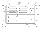
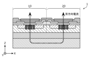
図1は半導体装置の構造の一例を示す断面図である。図2Aはその典型例としての平面図であり、半導体装置は矩形状であることを除いては、その大きさや形状は一例である。またパッドの大きさや形状および配置も一例である。図2Bは、半導体装置に流れる主電流を模式的に示す断面図である。図1および図2Bは、図2AのI-Iに沿って切断したときの切断面である。ところで、本開示においては、長方形という用語には正方形は含まれないと定義する。長方形であっても正方形であってもよい場合には、矩形という用語を用いで区別するものとする。
以下の説明では、トランジスタ10とトランジスタ20とが、第1導電型をN型、第2導電型をP型とした、いわゆるNチャネル型トランジスタの場合として、半導体装置1の導通動作について説明する。
以降の説明では、本実施形態1における半導体装置1が奏する効果について説明する。
以下、実施形態1に係る半導体装置1から、一部が変更されて構成される実施形態2に係る半導体装置1Aについて説明する。本実施形態2に係る半導体装置1Aについて、半導体装置1と同様の構成要素については、既に説明済みであるとして同じ符号を振ってその詳細な説明を省略し、半導体装置1との相違点を中心に説明する。
実施形態1の中で、双方向の導通を制御できるデュアル構成の縦型MOSトランジスタにおいて、一方の縦型MOSトランジスタと他方の縦型MOSトランジスタとを、表面側(パッド面側)から区別できることの利点に言及した。本実施形態3では、上記利点に特化したときの構造特徴について記載する。
10、10A、10B、トランジスタ(第1の縦型MOSトランジスタ)
11、11B 第1のソース電極
12、13、13B 部分
14 第1のソース領域
15 第1のゲート導体
16 第1のゲート絶縁膜
17 第1のゲートトレンチ
18 第1のボディ領域
18a 第1の接続部
19、19A、19B 第1のゲート電極
20、20B トランジスタ(第2の縦型MOSトランジスタ)
21、21B 第2のソース電極
22、23、23B 部分
24 第2のソース領域
25 第2のゲート導体
26 第2のゲート絶縁膜
27 第2のゲートトレンチ
28 第2のボディ領域
28a 第2の接続部
29、29B 第2のゲート電極
30 金属層
32 半導体基板
33 低濃度不純物層またはドリフト層
34 層間絶縁層
35 パッシベーション層
40 半導体層
90、90B 境界線
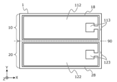
111、111B 第1のソースパッド
112、112A、112B 第1の活性領域
113、113A、113B 第1の周辺領域
114、114A、114B 第1のゲート配線(第1のゲートランナー)
114b 接続部分
115 第1のゲート抵抗素子
116、116A 第1のEQR
119、119B 第1のゲートパッド
121、121B 第2のソースパッド
122、122B 第2の活性領域
123、123B 第2の周辺領域
124、124B 第2のゲート配線(第2のゲートランナー)
125 第2のゲート抵抗素子
126 第2のEQR
129、129B 第2のゲートパッド
301 第1の辺
302 第2の辺
303 第3の辺
304 第4の辺
A1、A1B 第1の領域
A2、A2B 第2の領域
X 目印、目印となる個所
Claims (7)
- フェイスダウン実装が可能なチップサイズパッケージ型の半導体装置であって、
半導体基板と、
前記半導体基板上に形成された半導体層と、
前記半導体層の第1の領域に形成された、複数の第1のゲートトレンチを有する第1の縦型MOSトランジスタと、
前記半導体層の平面視において、前記第1の領域に隣接した第2の領域に形成された、複数の第2のゲートトレンチを有する第2の縦型MOSトランジスタと、
前記半導体基板の裏面に接触して形成された金属層と、を備え、
前記半導体基板は、前記第1の縦型MOSトランジスタおよび前記第2の縦型MOSトランジスタの共通ドレイン領域であり、
前記平面視において、前記半導体層は矩形状であり、前記半導体層の長辺の長さが前記第1の領域の外周を成す辺のうち最長の辺の長さと一致するように、前記第1の領域と前記第2の領域とは前記半導体層を面積で二等分する一方と他方とであり、
前記第1の領域には前記第1の縦型MOSトランジスタの導通を制御する第1のゲート電極と、前記第1のゲート電極と接続された第1のゲート配線とが備わり、
前記第2の領域には前記第2の縦型MOSトランジスタの導通を制御する第2のゲート電極と、前記第2のゲート電極と接続された第2のゲート配線とが備わり、
前記平面視において、前記第1のゲート電極と前記第1のゲート配線とが成す形状と、前記第2のゲート電極と前記第2のゲート配線とが成す形状とは、前記第1の領域と前記第2の領域との境界線を対称の軸とする線対称の関係になく、
前記平面視において、前記第1のゲート電極と前記第1のゲート配線とが成す形状と、前記第2のゲート電極と前記第2のゲート配線とが成す形状とは、前記半導体層の中心を対称の中心とする点対称の関係になく、
前記平面視において、前記第1の領域と前記第2の領域は各々長方形状であり、
前記平面視において、前記複数の第1のゲートトレンチが延在する方向は、前記第1の領域の短辺と平行する方向であり、
前記平面視において、前記複数の第2のゲートトレンチが延在する方向は、前記第2の領域の長辺と平行する方向である
半導体装置。 - フェイスダウン実装が可能なチップサイズパッケージ型の半導体装置であって、
半導体基板と、
前記半導体基板上に形成された半導体層と、
前記半導体層の第1の領域に形成された、複数の第1のゲートトレンチを有する第1の縦型MOSトランジスタと、
前記半導体層の平面視において、前記第1の領域に隣接した第2の領域に形成された、複数の第2のゲートトレンチを有する第2の縦型MOSトランジスタと、
前記半導体基板の裏面に接触して形成された金属層と、を備え、
前記半導体基板は、前記第1の縦型MOSトランジスタおよび前記第2の縦型MOSトランジスタの共通ドレイン領域であり、
前記平面視において、前記半導体層は矩形状であり、前記半導体層の長辺の長さが前記第1の領域の外周を成す辺のうち最長の辺の長さと一致するように、前記第1の領域と前記第2の領域とは前記半導体層を面積で二等分する一方と他方とであり、
前記第1の領域には前記第1の縦型MOSトランジスタの導通を制御する第1のゲート電極と、前記第1のゲート電極と接続された第1のゲート配線とが備わり、
前記第2の領域には前記第2の縦型MOSトランジスタの導通を制御する第2のゲート電極と、前記第2のゲート電極と接続された第2のゲート配線とが備わり、
前記平面視において、前記第1のゲート電極と前記第1のゲート配線とが成す形状と、前記第2のゲート電極と前記第2のゲート配線とが成す形状とは、前記第1の領域と前記第2の領域との境界線を対称の軸とする線対称の関係になく、
前記平面視において、前記第1のゲート電極と前記第1のゲート配線とが成す形状と、前記第2のゲート電極と前記第2のゲート配線とが成す形状とは、前記半導体層の中心を対称の中心とする点対称の関係になく、
前記第1のゲート電極と前記第1のゲート配線とは連続しており、
前記第2のゲート電極と前記第2のゲート配線とは連続しておらず、前記第2のゲート電極は前記第2のゲート配線と、ゲート抵抗素子を直列に介して接続される
半導体装置。 - フェイスダウン実装が可能なチップサイズパッケージ型の半導体装置であって、
半導体基板と、
前記半導体基板上に形成された半導体層と、
前記半導体層の第1の領域に形成された、複数の第1のゲートトレンチを有する第1の縦型MOSトランジスタと、
前記半導体層の平面視において、前記第1の領域に隣接した第2の領域に形成された、複数の第2のゲートトレンチを有する第2の縦型MOSトランジスタと、
前記半導体基板の裏面に接触して形成された金属層と、を備え、
前記半導体基板は、前記第1の縦型MOSトランジスタおよび前記第2の縦型MOSトランジスタの共通ドレイン領域であり、
前記平面視において、前記半導体層は矩形状であり、前記半導体層の長辺の長さが前記第1の領域の外周を成す辺のうち最長の辺の長さと一致するように、前記第1の領域と前記第2の領域とは前記半導体層を面積で二等分する一方と他方とであり、
前記第1の領域には前記第1の縦型MOSトランジスタの導通を制御する第1のゲート電極と、前記第1のゲート電極と接続された第1のゲート配線とが備わり、
前記第2の領域には前記第2の縦型MOSトランジスタの導通を制御する第2のゲート電極と、前記第2のゲート電極と接続された第2のゲート配線とが備わり、
前記平面視において、前記第1のゲート電極と前記第1のゲート配線とが成す形状と、前記第2のゲート電極と前記第2のゲート配線とが成す形状とは、前記第1の領域と前記第2の領域との境界線を対称の軸とする線対称の関係になく、
前記平面視において、前記第1のゲート電極と前記第1のゲート配線とが成す形状と、前記第2のゲート電極と前記第2のゲート配線とが成す形状とは、前記半導体層の中心を対称の中心とする点対称の関係になく、
前記平面視において、前記第1の領域と前記第2の領域は各々長方形状であり、
前記平面視において、前記複数の第1のゲートトレンチが延在する方向は、前記第1の領域の短辺と平行する方向であり、
前記平面視において、前記第1の領域の外周を成す4辺のうち、前記境界線と重複する辺を第1の辺とし、前記第1の辺に対向する辺を第2の辺とし、前記第1の辺および前記第2の辺に直交し、互いに対向する一方を第3の辺、他方を第4の辺とすると、
前記第1のゲート配線は少なくとも前記第1の辺、前記第2の辺、前記第3の辺の略全長に沿って連続して設置されており、
前記複数の第1のゲートトレンチは、前記第1のゲート配線と、前記第1のゲート配線のうち前記第1の辺に沿った部分と前記第2の辺に沿った部分との両方において接続されるものが最も多く、
前記第1のゲート配線は前記第4の辺に沿った部分には設置されない
半導体装置。 - フェイスダウン実装が可能なチップサイズパッケージ型の半導体装置であって、
半導体基板と、
前記半導体基板上に形成された半導体層と、
前記半導体層の第1の領域に形成された、複数の第1のゲートトレンチを有する第1の縦型MOSトランジスタと、
前記半導体層の平面視において、前記第1の領域に隣接した第2の領域に形成された、複数の第2のゲートトレンチを有する第2の縦型MOSトランジスタと、
前記半導体基板の裏面に接触して形成された金属層と、を備え、
前記半導体基板は、前記第1の縦型MOSトランジスタおよび前記第2の縦型MOSトランジスタの共通ドレイン領域であり、
前記平面視において、前記半導体層は矩形状であり、前記半導体層の長辺の長さが前記第1の領域の外周を成す辺のうち最長の辺の長さと一致するように、前記第1の領域と前記第2の領域とは前記半導体層を面積で二等分する一方と他方とであり、
前記第1の領域には前記第1の縦型MOSトランジスタの導通を制御する第1のゲート電極と、前記第1のゲート電極と接続された第1のゲート配線とが備わり、
前記第2の領域には前記第2の縦型MOSトランジスタの導通を制御する第2のゲート電極と、前記第2のゲート電極と接続された第2のゲート配線とが備わり、
前記平面視において、前記第1のゲート電極と前記第1のゲート配線とが成す形状と、前記第2のゲート電極と前記第2のゲート配線とが成す形状とは、前記第1の領域と前記第2の領域との境界線を対称の軸とする線対称の関係になく、
前記平面視において、前記第1のゲート電極と前記第1のゲート配線とが成す形状と、前記第2のゲート電極と前記第2のゲート配線とが成す形状とは、前記半導体層の中心を対称の中心とする点対称の関係になく、
前記平面視において、前記第1の領域と前記第2の領域は各々長方形状であり、
前記平面視において、前記複数の第1のゲートトレンチが延在する方向は、前記第1の領域の短辺と平行する方向であり、
前記平面視において、前記第1の領域の外周を成す4辺のうち、前記境界線と重複する辺を第1の辺とし、前記第1の辺に対向する辺を第2の辺とし、前記第1の辺および前記第2の辺に直交し、互いに対向する一方を第3の辺、他方を第4の辺とすると、
前記第1のゲート配線は少なくとも前記第1の辺、前記第2の辺、前記第3の辺の略全長に沿って連続して設置されており、
前記複数の第1のゲートトレンチは、前記第1のゲート配線と、前記第1のゲート配線のうち前記第1の辺に沿った部分と前記第2の辺に沿った部分との両方において接続されるものが最も多く、
さらに前記第1の領域には第1のEQRが備わり、
前記第1のEQRは前記第1の辺、前記第2の辺、前記第3の辺の略全長に沿って連続して設置され、前記第4の辺に沿った部分には設置されない
半導体装置。 - 前記平面視において、前記複数の第1のゲートトレンチのうち、前記第4の辺に最も近接するものと前記第4の辺との間の距離が、前記複数の第1のゲートトレンチのうち、前記第3の辺に最も近接するものと前記第3の辺との間の距離よりも小さい
請求項3または4に記載の半導体装置。 - 前記平面視において、前記第1のゲート配線は、前記第3の辺に沿った部分あるいは前記第4の辺に沿った部分の他に、前記第1の辺に沿った部分と前記第2の辺に沿った部分とを最短で接続する部分を有する
請求項5に記載の半導体装置。 - 前記第1の縦型MOSトランジスタの総ゲート幅と前記第2の縦型MOSトランジスタの総ゲート幅とは同等である
請求項6に記載の半導体装置。
Priority Applications (1)
| Application Number | Priority Date | Filing Date | Title |
|---|---|---|---|
| JP2024023534A JP2024046689A (ja) | 2022-07-22 | 2024-02-20 | 半導体装置 |
Applications Claiming Priority (3)
| Application Number | Priority Date | Filing Date | Title |
|---|---|---|---|
| US202263391463P | 2022-07-22 | 2022-07-22 | |
| US63/391,463 | 2022-07-22 | ||
| PCT/JP2023/016405 WO2024018715A1 (ja) | 2022-07-22 | 2023-04-26 | 半導体装置 |
Related Child Applications (1)
| Application Number | Title | Priority Date | Filing Date |
|---|---|---|---|
| JP2024023534A Division JP2024046689A (ja) | 2022-07-22 | 2024-02-20 | 半導体装置 |
Publications (1)
| Publication Number | Publication Date |
|---|---|
| JP7442750B1 true JP7442750B1 (ja) | 2024-03-04 |
Family
ID=89491233
Family Applications (2)
| Application Number | Title | Priority Date | Filing Date |
|---|---|---|---|
| JP2023563899A Active JP7442750B1 (ja) | 2022-07-22 | 2023-04-26 | 半導体装置 |
| JP2024023534A Pending JP2024046689A (ja) | 2022-07-22 | 2024-02-20 | 半導体装置 |
Family Applications After (1)
| Application Number | Title | Priority Date | Filing Date |
|---|---|---|---|
| JP2024023534A Pending JP2024046689A (ja) | 2022-07-22 | 2024-02-20 | 半導体装置 |
Country Status (2)
| Country | Link |
|---|---|
| JP (2) | JP7442750B1 (ja) |
| CN (1) | CN117413361A (ja) |
Citations (5)
| Publication number | Priority date | Publication date | Assignee | Title |
|---|---|---|---|---|
| JP2005011986A (ja) | 2003-06-19 | 2005-01-13 | Sanyo Electric Co Ltd | 半導体装置 |
| JP2005302952A (ja) | 2004-04-09 | 2005-10-27 | Toshiba Corp | 半導体装置 |
| US20110233605A1 (en) | 2010-03-26 | 2011-09-29 | Force Mos Technology Co. Ltd. | Semiconductor power device layout for stress reduction |
| JP2019161168A (ja) | 2018-03-16 | 2019-09-19 | 富士電機株式会社 | 半導体装置 |
| JP2022026643A (ja) | 2020-07-31 | 2022-02-10 | ローム株式会社 | 半導体装置 |
Family Cites Families (2)
| Publication number | Priority date | Publication date | Assignee | Title |
|---|---|---|---|---|
| JP2007129250A (ja) * | 2006-12-20 | 2007-05-24 | Fujitsu Ltd | 半導体装置 |
| KR102308044B1 (ko) * | 2018-12-19 | 2021-10-01 | 누보톤 테크놀로지 재팬 가부시키가이샤 | 반도체 장치 |
-
2023
- 2023-04-26 CN CN202380011458.4A patent/CN117413361A/zh active Pending
- 2023-04-26 JP JP2023563899A patent/JP7442750B1/ja active Active
-
2024
- 2024-02-20 JP JP2024023534A patent/JP2024046689A/ja active Pending
Patent Citations (5)
| Publication number | Priority date | Publication date | Assignee | Title |
|---|---|---|---|---|
| JP2005011986A (ja) | 2003-06-19 | 2005-01-13 | Sanyo Electric Co Ltd | 半導体装置 |
| JP2005302952A (ja) | 2004-04-09 | 2005-10-27 | Toshiba Corp | 半導体装置 |
| US20110233605A1 (en) | 2010-03-26 | 2011-09-29 | Force Mos Technology Co. Ltd. | Semiconductor power device layout for stress reduction |
| JP2019161168A (ja) | 2018-03-16 | 2019-09-19 | 富士電機株式会社 | 半導体装置 |
| JP2022026643A (ja) | 2020-07-31 | 2022-02-10 | ローム株式会社 | 半導体装置 |
Also Published As
| Publication number | Publication date |
|---|---|
| CN117413361A (zh) | 2024-01-16 |
| JP2024046689A (ja) | 2024-04-03 |
Similar Documents
| Publication | Publication Date | Title |
|---|---|---|
| US11908868B2 (en) | Semiconductor device | |
| CN111463278B (zh) | 半导体装置 | |
| JP5511124B2 (ja) | 絶縁ゲート型半導体装置 | |
| US10566448B2 (en) | Insulated gate bipolar transistor | |
| TW201721835A (zh) | 半導體裝置及其製造方法 | |
| US11088276B2 (en) | Silicon carbide semiconductor device | |
| JP6941502B2 (ja) | 半導体装置および半導体パッケージ | |
| US6992351B2 (en) | Semiconductor device for power MOS transistor module | |
| JP7243845B2 (ja) | 半導体装置 | |
| JP7442750B1 (ja) | 半導体装置 | |
| WO2024018715A1 (ja) | 半導体装置 | |
| US4520382A (en) | Semiconductor integrated circuit with inversion preventing electrode | |
| JP2020129595A (ja) | 半導体装置 | |
| US6940128B1 (en) | Semiconductor device for power MOS transistor module | |
| WO2024090243A1 (ja) | 半導体装置 | |
| US20240153955A1 (en) | Semiconductor device | |
| JP7475569B1 (ja) | 半導体装置 | |
| US20220285337A1 (en) | Semiconductor device and semiconductor storage device | |
| US20230085094A1 (en) | Semiconductor device | |
| US20240014299A1 (en) | Semiconductor device | |
| JP2023085505A (ja) | 半導体装置 |
Legal Events
| Date | Code | Title | Description |
|---|---|---|---|
| A521 | Request for written amendment filed |
Free format text: JAPANESE INTERMEDIATE CODE: A523 Effective date: 20231017 |
|
| A621 | Written request for application examination |
Free format text: JAPANESE INTERMEDIATE CODE: A621 Effective date: 20231017 |
|
| A871 | Explanation of circumstances concerning accelerated examination |
Free format text: JAPANESE INTERMEDIATE CODE: A871 Effective date: 20231017 |
|
| TRDD | Decision of grant or rejection written | ||
| A01 | Written decision to grant a patent or to grant a registration (utility model) |
Free format text: JAPANESE INTERMEDIATE CODE: A01 Effective date: 20240130 |
|
| A61 | First payment of annual fees (during grant procedure) |
Free format text: JAPANESE INTERMEDIATE CODE: A61 Effective date: 20240220 |
|
| R150 | Certificate of patent or registration of utility model |
Ref document number: 7442750 Country of ref document: JP Free format text: JAPANESE INTERMEDIATE CODE: R150 |