JP7321009B2 - Wiring board, junction type wiring board, and method for manufacturing wiring board - Google Patents
Wiring board, junction type wiring board, and method for manufacturing wiring board Download PDFInfo
- Publication number
- JP7321009B2 JP7321009B2 JP2019123233A JP2019123233A JP7321009B2 JP 7321009 B2 JP7321009 B2 JP 7321009B2 JP 2019123233 A JP2019123233 A JP 2019123233A JP 2019123233 A JP2019123233 A JP 2019123233A JP 7321009 B2 JP7321009 B2 JP 7321009B2
- Authority
- JP
- Japan
- Prior art keywords
- posts
- wiring
- layer
- wiring board
- post
- Prior art date
- Legal status (The legal status is an assumption and is not a legal conclusion. Google has not performed a legal analysis and makes no representation as to the accuracy of the status listed.)
- Active
Links
Images


Classifications
-
- H—ELECTRICITY
- H01—ELECTRIC ELEMENTS
- H01L—SEMICONDUCTOR DEVICES NOT COVERED BY CLASS H10
- H01L23/00—Details of semiconductor or other solid state devices
- H01L23/48—Arrangements for conducting electric current to or from the solid state body in operation, e.g. leads, terminal arrangements ; Selection of materials therefor
- H01L23/488—Arrangements for conducting electric current to or from the solid state body in operation, e.g. leads, terminal arrangements ; Selection of materials therefor consisting of soldered or bonded constructions
- H01L23/498—Leads, i.e. metallisations or lead-frames on insulating substrates, e.g. chip carriers
- H01L23/49838—Geometry or layout
-
- H—ELECTRICITY
- H05—ELECTRIC TECHNIQUES NOT OTHERWISE PROVIDED FOR
- H05K—PRINTED CIRCUITS; CASINGS OR CONSTRUCTIONAL DETAILS OF ELECTRIC APPARATUS; MANUFACTURE OF ASSEMBLAGES OF ELECTRICAL COMPONENTS
- H05K1/00—Printed circuits
- H05K1/02—Details
- H05K1/0296—Conductive pattern lay-out details not covered by sub groups H05K1/02 - H05K1/0295
- H05K1/0298—Multilayer circuits
-
- H—ELECTRICITY
- H01—ELECTRIC ELEMENTS
- H01L—SEMICONDUCTOR DEVICES NOT COVERED BY CLASS H10
- H01L24/00—Arrangements for connecting or disconnecting semiconductor or solid-state bodies; Methods or apparatus related thereto
- H01L24/01—Means for bonding being attached to, or being formed on, the surface to be connected, e.g. chip-to-package, die-attach, "first-level" interconnects; Manufacturing methods related thereto
- H01L24/26—Layer connectors, e.g. plate connectors, solder or adhesive layers; Manufacturing methods related thereto
- H01L24/28—Structure, shape, material or disposition of the layer connectors prior to the connecting process
- H01L24/29—Structure, shape, material or disposition of the layer connectors prior to the connecting process of an individual layer connector
-
- H—ELECTRICITY
- H05—ELECTRIC TECHNIQUES NOT OTHERWISE PROVIDED FOR
- H05K—PRINTED CIRCUITS; CASINGS OR CONSTRUCTIONAL DETAILS OF ELECTRIC APPARATUS; MANUFACTURE OF ASSEMBLAGES OF ELECTRICAL COMPONENTS
- H05K1/00—Printed circuits
- H05K1/02—Details
- H05K1/11—Printed elements for providing electric connections to or between printed circuits
- H05K1/111—Pads for surface mounting, e.g. lay-out
-
- H—ELECTRICITY
- H05—ELECTRIC TECHNIQUES NOT OTHERWISE PROVIDED FOR
- H05K—PRINTED CIRCUITS; CASINGS OR CONSTRUCTIONAL DETAILS OF ELECTRIC APPARATUS; MANUFACTURE OF ASSEMBLAGES OF ELECTRICAL COMPONENTS
- H05K3/00—Apparatus or processes for manufacturing printed circuits
- H05K3/30—Assembling printed circuits with electric components, e.g. with resistor
- H05K3/32—Assembling printed circuits with electric components, e.g. with resistor electrically connecting electric components or wires to printed circuits
- H05K3/34—Assembling printed circuits with electric components, e.g. with resistor electrically connecting electric components or wires to printed circuits by soldering
- H05K3/341—Surface mounted components
- H05K3/3431—Leadless components
- H05K3/3436—Leadless components having an array of bottom contacts, e.g. pad grid array or ball grid array components
-
- H—ELECTRICITY
- H05—ELECTRIC TECHNIQUES NOT OTHERWISE PROVIDED FOR
- H05K—PRINTED CIRCUITS; CASINGS OR CONSTRUCTIONAL DETAILS OF ELECTRIC APPARATUS; MANUFACTURE OF ASSEMBLAGES OF ELECTRICAL COMPONENTS
- H05K3/00—Apparatus or processes for manufacturing printed circuits
- H05K3/40—Forming printed elements for providing electric connections to or between printed circuits
- H05K3/4007—Surface contacts, e.g. bumps
-
- H—ELECTRICITY
- H05—ELECTRIC TECHNIQUES NOT OTHERWISE PROVIDED FOR
- H05K—PRINTED CIRCUITS; CASINGS OR CONSTRUCTIONAL DETAILS OF ELECTRIC APPARATUS; MANUFACTURE OF ASSEMBLAGES OF ELECTRICAL COMPONENTS
- H05K3/00—Apparatus or processes for manufacturing printed circuits
- H05K3/46—Manufacturing multilayer circuits
- H05K3/4602—Manufacturing multilayer circuits characterized by a special circuit board as base or central core whereon additional circuit layers are built or additional circuit boards are laminated
- H05K3/4605—Manufacturing multilayer circuits characterized by a special circuit board as base or central core whereon additional circuit layers are built or additional circuit boards are laminated made from inorganic insulating material
-
- H—ELECTRICITY
- H01—ELECTRIC ELEMENTS
- H01L—SEMICONDUCTOR DEVICES NOT COVERED BY CLASS H10
- H01L23/00—Details of semiconductor or other solid state devices
- H01L23/48—Arrangements for conducting electric current to or from the solid state body in operation, e.g. leads, terminal arrangements ; Selection of materials therefor
- H01L23/488—Arrangements for conducting electric current to or from the solid state body in operation, e.g. leads, terminal arrangements ; Selection of materials therefor consisting of soldered or bonded constructions
- H01L23/498—Leads, i.e. metallisations or lead-frames on insulating substrates, e.g. chip carriers
- H01L23/49822—Multilayer substrates
-
- H—ELECTRICITY
- H01—ELECTRIC ELEMENTS
- H01L—SEMICONDUCTOR DEVICES NOT COVERED BY CLASS H10
- H01L23/00—Details of semiconductor or other solid state devices
- H01L23/48—Arrangements for conducting electric current to or from the solid state body in operation, e.g. leads, terminal arrangements ; Selection of materials therefor
- H01L23/488—Arrangements for conducting electric current to or from the solid state body in operation, e.g. leads, terminal arrangements ; Selection of materials therefor consisting of soldered or bonded constructions
- H01L23/498—Leads, i.e. metallisations or lead-frames on insulating substrates, e.g. chip carriers
- H01L23/49827—Via connections through the substrates, e.g. pins going through the substrate, coaxial cables
-
- H—ELECTRICITY
- H01—ELECTRIC ELEMENTS
- H01L—SEMICONDUCTOR DEVICES NOT COVERED BY CLASS H10
- H01L23/00—Details of semiconductor or other solid state devices
- H01L23/48—Arrangements for conducting electric current to or from the solid state body in operation, e.g. leads, terminal arrangements ; Selection of materials therefor
- H01L23/488—Arrangements for conducting electric current to or from the solid state body in operation, e.g. leads, terminal arrangements ; Selection of materials therefor consisting of soldered or bonded constructions
- H01L23/498—Leads, i.e. metallisations or lead-frames on insulating substrates, e.g. chip carriers
- H01L23/49833—Leads, i.e. metallisations or lead-frames on insulating substrates, e.g. chip carriers the chip support structure consisting of a plurality of insulating substrates
-
- H—ELECTRICITY
- H05—ELECTRIC TECHNIQUES NOT OTHERWISE PROVIDED FOR
- H05K—PRINTED CIRCUITS; CASINGS OR CONSTRUCTIONAL DETAILS OF ELECTRIC APPARATUS; MANUFACTURE OF ASSEMBLAGES OF ELECTRICAL COMPONENTS
- H05K2201/00—Indexing scheme relating to printed circuits covered by H05K1/00
- H05K2201/09—Shape and layout
- H05K2201/09209—Shape and layout details of conductors
- H05K2201/09372—Pads and lands
- H05K2201/094—Array of pads or lands differing from one another, e.g. in size, pitch, thickness; Using different connections on the pads
-
- H—ELECTRICITY
- H05—ELECTRIC TECHNIQUES NOT OTHERWISE PROVIDED FOR
- H05K—PRINTED CIRCUITS; CASINGS OR CONSTRUCTIONAL DETAILS OF ELECTRIC APPARATUS; MANUFACTURE OF ASSEMBLAGES OF ELECTRICAL COMPONENTS
- H05K2201/00—Indexing scheme relating to printed circuits covered by H05K1/00
- H05K2201/09—Shape and layout
- H05K2201/09209—Shape and layout details of conductors
- H05K2201/09372—Pads and lands
- H05K2201/09427—Special relation between the location or dimension of a pad or land and the location or dimension of a terminal
-
- H—ELECTRICITY
- H05—ELECTRIC TECHNIQUES NOT OTHERWISE PROVIDED FOR
- H05K—PRINTED CIRCUITS; CASINGS OR CONSTRUCTIONAL DETAILS OF ELECTRIC APPARATUS; MANUFACTURE OF ASSEMBLAGES OF ELECTRICAL COMPONENTS
- H05K2201/00—Indexing scheme relating to printed circuits covered by H05K1/00
- H05K2201/09—Shape and layout
- H05K2201/09209—Shape and layout details of conductors
- H05K2201/09654—Shape and layout details of conductors covering at least two types of conductors provided for in H05K2201/09218 - H05K2201/095
- H05K2201/09781—Dummy conductors, i.e. not used for normal transport of current; Dummy electrodes of components
-
- H—ELECTRICITY
- H05—ELECTRIC TECHNIQUES NOT OTHERWISE PROVIDED FOR
- H05K—PRINTED CIRCUITS; CASINGS OR CONSTRUCTIONAL DETAILS OF ELECTRIC APPARATUS; MANUFACTURE OF ASSEMBLAGES OF ELECTRICAL COMPONENTS
- H05K2203/00—Indexing scheme relating to apparatus or processes for manufacturing printed circuits covered by H05K3/00
- H05K2203/04—Soldering or other types of metallurgic bonding
- H05K2203/049—Wire bonding
-
- H—ELECTRICITY
- H05—ELECTRIC TECHNIQUES NOT OTHERWISE PROVIDED FOR
- H05K—PRINTED CIRCUITS; CASINGS OR CONSTRUCTIONAL DETAILS OF ELECTRIC APPARATUS; MANUFACTURE OF ASSEMBLAGES OF ELECTRICAL COMPONENTS
- H05K2203/00—Indexing scheme relating to apparatus or processes for manufacturing printed circuits covered by H05K3/00
- H05K2203/05—Patterning and lithography; Masks; Details of resist
- H05K2203/0562—Details of resist
- H05K2203/0574—Stacked resist layers used for different processes
-
- Y—GENERAL TAGGING OF NEW TECHNOLOGICAL DEVELOPMENTS; GENERAL TAGGING OF CROSS-SECTIONAL TECHNOLOGIES SPANNING OVER SEVERAL SECTIONS OF THE IPC; TECHNICAL SUBJECTS COVERED BY FORMER USPC CROSS-REFERENCE ART COLLECTIONS [XRACs] AND DIGESTS
- Y02—TECHNOLOGIES OR APPLICATIONS FOR MITIGATION OR ADAPTATION AGAINST CLIMATE CHANGE
- Y02P—CLIMATE CHANGE MITIGATION TECHNOLOGIES IN THE PRODUCTION OR PROCESSING OF GOODS
- Y02P70/00—Climate change mitigation technologies in the production process for final industrial or consumer products
- Y02P70/50—Manufacturing or production processes characterised by the final manufactured product
Description
本発明は、配線基板、接合型配線基板及び配線基板の製造方法に関する。 The present invention relates to a wiring board, a junction-type wiring board, and a method for manufacturing a wiring board.
近年、半導体装置の高集積化及び微細化を促進するために、複数の配線基板を立体的に重ねて実装する3次元実装が検討されている。このような3次元実装では、例えば主基板上に、微細配線を有する中継基板が接合されることがある。具体的には、主基板と中継基板の間に、例えばNCF(Non-Conductive Film)などのアンダーフィル材が充填され、中継基板が主基板に接合される。また、主基板の表面には導電体のポストが形成されており、このポストと中継基板の表面に形成された電極パッドとがはんだによって接続される。これにより、主基板と中継基板が電気的に接続される。 2. Description of the Related Art In recent years, in order to promote high integration and miniaturization of semiconductor devices, three-dimensional packaging, in which a plurality of wiring substrates are three-dimensionally stacked and mounted, has been studied. In such three-dimensional mounting, for example, a relay substrate having fine wiring is sometimes bonded onto a main substrate. Specifically, an underfill material such as NCF (Non-Conductive Film) is filled between the main board and the relay board, and the relay board is joined to the main board. Conductive posts are formed on the surface of the main board, and these posts are connected to electrode pads formed on the surface of the relay board by soldering. Thereby, the main board and the relay board are electrically connected.
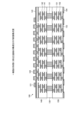
主基板と中継基板が接合される際には、配線基板間にアンダーフィル材が充填された状態で、両配線基板が互いに近づく方向に加圧される。このとき、アンダーフィル材は、配線基板間から溢れ出し、例えば中継基板の周囲にフィレットを形成する。すなわち、例えば図11に示すように、主基板10に中継基板20が接合される場合、両配線基板の間から排出されるアンダーフィル材によって、中継基板20の周囲にフィレット30が形成される。なお、図11は、主基板10と中継基板20とを接合した接合型配線基板を中継基板20側から見た平面図である。
When the main board and the relay board are joined together, the wiring boards are pressed toward each other while the underfill material is filled between the wiring boards. At this time, the underfill material overflows from between the wiring boards and forms a fillet around the relay board, for example. That is, as shown in FIG. 11, for example, when the
しかしながら、上記の接合型配線基板においては、中継基板の周囲に形成されるフィレットの形状が一様ではなく、主基板上の部品実装領域が制限されるという問題がある。具体的には、図11に示したように、中継基板20の四辺の中央部分においてフィレット30が大きく広がり、中継基板20の近傍に部品を実装することが困難である。
However, the junction-type wiring board described above has a problem that the shape of the fillet formed around the relay board is not uniform, and the component mounting area on the main board is limited. Specifically, as shown in FIG. 11, the
また、中継基板20の四隅部分においてはフィレット30の広がりが小さいが、中央部分でフィレット30が大きく広がっているため、主基板10上に位置を揃えて部品を実装することが困難であり、部品配置の柔軟性が損なわれる。
In addition, although the spread of the
開示の技術は、かかる点に鑑みてなされたものであって、フィレットの形状を調節することができる配線基板、接合型配線基板及び配線基板の製造方法を提供することを目的とする。 The disclosed technique has been made in view of the above points, and aims to provide a wiring board, a junction-type wiring board, and a method of manufacturing a wiring board that can adjust the shape of the fillet.
本願が開示する配線基板は、1つの態様において、積層された配線層及び絶縁層を備えた配線構造体と、前記配線構造体の表面の所定の領域の周縁に沿って形成され、前記配線構造体の表面から突出している複数の第1のポストと、前記複数の第1のポストによって囲まれた位置で前記配線層に接続し、前記配線構造体の表面から突出している第2のポストと、を有し、前記複数の第1のポストは、前記所定の領域の周縁を構成する辺の中央部に配置されているポストが、前記辺の両端部に配置されているポストよりも、前記配線構造体の表面からの高さが低い。 In one aspect, a wiring substrate disclosed in the present application is formed along a peripheral edge of a predetermined region on a surface of the wiring structure, and a wiring structure including a laminated wiring layer and an insulating layer. a plurality of first posts protruding from the surface of the body; and second posts protruding from the surface of the wiring structure, connected to the wiring layer at positions surrounded by the plurality of first posts. , wherein the plurality of first posts are arranged such that the posts arranged in the central portion of the side forming the peripheral edge of the predetermined area are arranged more than the posts arranged at both ends of the side. The height from the surface of the wiring structure is small.
本願が開示する配線基板、接合型配線基板及び配線基板の製造方法の1つの態様によれば、フィレットの形状を調節することができるという効果を奏する。 According to one aspect of the wiring board, the bonding type wiring board, and the wiring board manufacturing method disclosed in the present application, there is an effect that the shape of the fillet can be adjusted.
以下、本願が開示する配線基板、接合型配線基板及び配線基板の製造方法の一実施の形態について、図面を参照して詳細に説明する。なお、この実施の形態により本発明が限定されるものではない。 An embodiment of a wiring board, a junction-type wiring board, and a method for manufacturing a wiring board disclosed in the present application will be described below in detail with reference to the drawings. It should be noted that the present invention is not limited by this embodiment.
図1は、一実施の形態に係る主基板100の構成を示す平面図である。この主基板100は、他の中継基板などを重ねて接合することにより、接合型配線基板を形成する。このため、主基板100は、他の中継基板が接合される接合領域110を有する。そして、接合領域110には、ダミーポスト121及び接続ポスト122が形成されている。
FIG. 1 is a plan view showing the configuration of a
ダミーポスト121は、接合領域110の周縁に沿って配列される導電体のポストである。ダミーポスト121は、主基板100の配線には接続されておらず、主基板100の表面の例えばソルダーレジスト層上に形成される。そして、ダミーポスト121は、主基板100と他の中継基板とが接合される際に、中継基板の周縁部に当接して支持する。
The
接合領域110の各辺に沿って並ぶダミーポスト121は、主基板100の表面からの高さが異なる。具体的には、辺の両端に配置されるダミーポスト121が最も高く、辺の中央へ向かうに連れてダミーポスト121が低くなる。このように高さが異なるダミーポスト121は、例えば電解銅めっきによって同時に形成される。電解銅めっきによって高さが異なるダミーポスト121が形成されるため、それぞれのダミーポスト121は径の大きさも異なっている。
The
接続ポスト122は、接合領域110のダミーポスト121に囲まれた領域に形成される導電体のポストである。接続ポスト122は、主基板100の配線に接続され、主基板100に接合される中継基板の電極パッドにはんだ付けされる。すなわち、接続ポスト122は、主基板100と中継基板を電気的に接続する。接続ポスト122は、主基板100の表面からの高さが等しく、径の大きさも均一である。また、接続ポスト122は、例えばダミーポスト121と同時に電解銅めっきによって形成される。なお、図1においては、接続ポスト122が格子状に配列されるものとしたが、接続ポスト122の配置はこれに限定されない。
The
図2は、図1のI-I線断面を示す模式図である。図2に示すように、主基板100は、複数の層が積層された積層基板である。具体的には、主基板100は、コア層130及びビルドアップ層140、150を有する。これらのコア層130及びビルドアップ層140、150は、主基板100の配線構造体を構成する。
FIG. 2 is a schematic diagram showing a cross section taken along line II of FIG. As shown in FIG. 2, the
コア層130は、絶縁性の基材の両面に、めっきにより配線層が形成されたものである。両面の配線層は、必要に応じてビア131によって接続される。
The
ビルドアップ層140は、コア層130の上面に形成され、例えばビルドアップ樹脂からなる絶縁層と導電体からなる配線層141とを備える層が積層されたものである。各配線層141は、ビア142によって接続される。また、ビルドアップ層140の表面は、ソルダーレジスト層143によって被覆される。ビルドアップ層140の表面にビア142が露出する位置においては、ソルダーレジスト層143に開口部が形成され、ビア142に接続する接続ポスト122が形成される。また、複数の接続ポスト122が並ぶ両端においては、ソルダーレジスト層143上にダミーポスト121が形成される。図2に示すダミーポスト121は、接合領域110の辺の中央に配置されたダミーポスト121であるため、主基板100の表面からの高さが接続ポスト122よりも低い。具体的には、例えば接続ポスト122の高さが例えば20μm程度であるのに対し、ダミーポスト121の高さは、例えば10μm程度である。
The
ビルドアップ層150は、コア層130の下面に形成され、例えばビルドアップ樹脂からなる絶縁層と導電体からなる配線層151とを備える層が積層されたものである。各配線層151は、ビア152によって接続される。また、ビルドアップ層150の表面には、例えば銅などの導電体により電極パッド153が形成され、主基板100がマザーボード等の外部部品に接合される際の接続端子となる。そして、ビルドアップ層150の表面は、電極パッド153を露出させるソルダーレジスト層154によって被覆される。
The
図3は、図1のII-II線断面を示す模式図である。すなわち、図3は、ダミーポスト121が配列された接合領域110の周縁における断面を示す。
FIG. 3 is a schematic diagram showing a cross section taken along line II--II of FIG. That is, FIG. 3 shows a cross section at the peripheral edge of the
図3に示すように、ソルダーレジスト層143上には複数のダミーポスト121が形成される。そして、接合領域110の辺の両端に配置されるダミーポスト121aは、辺の中央に配置されるダミーポスト121bよりも高い。すなわち、複数のダミーポスト121の主基板100の表面からの高さが異なっており、接合領域110の辺の両端から辺の中央へ向かうに連れてダミーポスト121の高さが低くなる。具体的には、辺の両端のダミーポスト121aの高さは、例えば25μm程度であり接続ポスト122よりも高いのに対し、辺の中央のダミーポスト121bの高さは、例えば10μm程度であり接続ポスト122よりも低い。また、これらのダミーポスト121は、例えば電解銅めっきによって同時に形成されるため、径の大きさが異なっている。すなわち、異なる大きさの径で電解銅めっきが施されることにより、めっきが成長する高さが異なり、同一時間の電解銅めっきにより高さが異なるダミーポスト121が形成される。
A plurality of
次いで、上記のように構成された主基板100の製造方法について、図4に示すフロー図を参照しながら説明する。
Next, a method for manufacturing the
まず、主基板100の支持部材となるコア層130が形成される(ステップS101)。具体的には、絶縁性の基材に、基材を貫通するビア131が形成されるとともに、基材の両面に例えば銅などの金属の配線層が形成される。基材の両面の配線層は、必要に応じて、ビア131によって接続されている。
First, a
そして、コア層130の上面及び下面にビルドアップ法によってビルドアップ層140、150が形成される(ステップS102)。具体的には、コア層130の上面に、絶縁層と配線層141とを有する層が積層されてビルドアップ層140が形成される。配線層141は、絶縁層を貫通するビア142によって接続される。また、コア層130の下面に、絶縁層と配線層151とを有する層が積層されてビルドアップ層150が形成される。配線層151は、絶縁層を貫通するビア152によって接続される。また、ビルドアップ層150の表面には、電極パッド153が形成される。絶縁層は、例えばエポキシ樹脂又はポリイミド樹脂等の絶縁樹脂を用いて形成される。また、配線層141、151、ビア142、152及び電極パッド153は、例えば銅などの金属のめっきによって形成される。
Then, buildup layers 140 and 150 are formed on the upper and lower surfaces of the
そして、ビルドアップ層140、150の表面にソルダーレジスト層143、154が形成される(ステップS103)。すなわち、ビルドアップ層140の表面がソルダーレジスト層143によって被覆され、ビルドアップ層150の表面がソルダーレジスト層154によって被覆される。ビルドアップ層140の最上層のビア142に対応する位置においては、ソルダーレジスト層143に開口部が穿設される。つまり、ビア142の上面がソルダーレジスト層143の開口部から露出する。一方、ビルドアップ層150の電極パッド153に対応する位置においては、ソルダーレジスト層154に開口部が穿設される。つまり、電極パッド153がソルダーレジスト層154の開口部から露出する。
Then, solder resist
続いて、ビルドアップ層140の表面の接合領域110に、ダミーポスト121及び接続ポスト122が形成される。具体的には、ビルドアップ層140の表面に例えば無電解銅めっき又はスパッタリングによってシード層が形成され、シード層にドライフィルムレジスト(DFR)が貼付される。そして、DFRのパターニングによって、ダミーポスト121及び接続ポスト122が形成される位置に開口部が穿設される(ステップS104)。
Subsequently, dummy posts 121 and
すなわち、例えば図5に示すように、シード層160上にDFR170が貼付され、ダミーポスト121が形成される位置に開口部171が形成され、接続ポスト122が形成される位置に開口部172が形成される。ここで、ダミーポスト121が形成される位置は、中継基板が接合される接合領域110の周縁であり、接続ポスト122が形成される位置は、ビルドアップ層140の最上層のビア142の上面が露出する位置である。したがって、開口部171は、接合領域110の周縁に穿設され、開口部172は、ビア142に対応する位置に穿設される。また、ダミーポスト121と接続ポスト122は、高さが異なることがあるため、それぞれの高さに応じて開口部171、172の径の大きさが異なる。
That is, for example, as shown in FIG. 5, the
DFR170のパターニングが行われると、電解銅めっきによって、ダミーポスト121及び接続ポスト122が形成される(ステップS105)。具体的には、例えば図6に示すように、DFR170の開口部171、172の径の大きさに応じて電解銅が析出し、開口部171にはダミーポスト121が形成され、開口部172には接続ポスト122が形成される。このように、DFR170の開口部の径の大きさに応じてめっきの成長量を調整することができるため、開口部171の径の大きさが適宜設定され、接合領域110の辺の両端で高く中央で低いダミーポスト121が形成される。ダミーポスト121は、ソルダーレジスト層143上に形成されており、ビルドアップ層140の配線層141には接続されていないが、接続ポスト122は、ビア142上に形成されており、ビルドアップ層140の配線層141と電気的に接続される。
After patterning the
そして、DFR170が剥離され(ステップS106)、シード層160のエッチングが行われる(ステップS107)。これにより、ダミーポスト121及び接続ポスト122が形成される部分以外のシード層160が除去され、例えば図7に示すように、ダミーポスト121及び接続ポスト122の基部にのみシード層160が残存する。このようにして、接合領域110の周縁にダミーポスト121が形成されるとともに、ダミーポスト121によって囲まれる領域に接続ポスト122が形成される。
Then, the
以上のようにして製造された主基板100は、他の中継基板と接合されることにより接合型配線基板を形成する。図8は、接合型配線基板の構成例を示す図である。図8に示す接合型配線基板は、主基板100に中継基板200が接合された構成を有する。
The
具体的には、中継基板200は、主基板100の接合領域110に、アンダーフィル材300によって接着される。また、中継基板200の下面には、電極パッド210が形成されており、電極パッド210は、はんだ310によって主基板100の接続ポスト122に接続される。
Specifically, the
中継基板200が接合される際には、主基板100の接合領域110にアンダーフィル材300が配置され、アンダーフィル材300を挟むように上方から中継基板200が載置される。そして、両配線基板が近づく方向に主基板100と中継基板200が加圧される。このとき、主基板100と中継基板200によって挟まれるアンダーフィル材300が中継基板200の周囲へ排出され、フィレットを形成する。本実施の形態においては、接合領域110の周縁にダミーポスト121が形成されているため、ダミーポスト121によって中継基板200の周縁部が支持され、アンダーフィル材300を排出する主基板100と中継基板200との間隙が規定される。
When the
具体的には、例えば図9に示すように、接合領域110の辺の両端から中央へ向かうに連れてダミーポスト121の高さが低くなるため、中継基板200の周縁部では、位置によって主基板100と中継基板200の間の距離が異なる。すなわち、中継基板200の四隅においては主基板100と中継基板200の間の距離が大きい一方、中継基板200の辺の中央部においては主基板100と中継基板200の間の距離が小さい。この結果、主基板100と中継基板200の間の距離が大きい中継基板200の四隅付近からは、比較的多くのアンダーフィル材300が排出される。これに対して、主基板100と中継基板200の間の距離が小さい中継基板200の辺の中央付近においては、中継基板200の周縁部によってアンダーフィル材300の排出が阻害され、排出されるアンダーフィル材300が比較的少ない。
Specifically, for example, as shown in FIG. 9, since the height of the
このように、ダミーポスト121の高さによって、排出されるアンダーフィル材300の量を調節する結果、中継基板200の周囲には、例えば図10に示すように、一様な大きさで広がるフィレット300aを形成することができる。すなわち、中継基板200の辺の位置に応じてダミーポスト121の高さが異なるため、それぞれのダミーポスト121の高さに応じてアンダーフィル材300の排出量が調整され、フィレット300aの形状を制御することができる。
As a result of adjusting the amount of the discharged
特に、中継基板200の辺の中央付近から周囲へ流出するアンダーフィル材300の量が制限されているため、辺の中央部分でフィレット300aが大きく広がることがない。このため、中継基板200の周囲のフィレット300aのサイズを一様にすることができ、主基板100上の中継基板200近傍に位置を揃えて部品を実装することが可能となる。さらに、ダミーポスト121が中継基板200の周縁部を支持するため、主基板100と中継基板200の間の距離が過度に小さくなることがなく、アンダーフィル材300を確実に中継基板200の周囲へ排出させることができる。結果として、主基板100と中継基板200に挟まれる余分なアンダーフィル材300を周囲へ排出させることができ、主基板100の接続ポスト122と中継基板200の電極パッド210とを確実に接触させることができる。
In particular, since the amount of
以上のように、本実施の形態によれば、中継基板と接合される主基板の接合領域の周縁に沿ってダミーポストを形成し、接合領域の辺の両端から中央へ向かうに連れてダミーポストの高さを低くする。このため、辺の両端よりも中央付近で主基板と中継基板の周縁部との距離が小さくなり、辺の中央付近から中継基板の周囲へ流出するアンダーフィル材の量が制限される。結果として、中継基板の辺の各所から流出するアンダーフィル材の量を一様にすることができ、フィレットの形状を調節することができる。 As described above, according to the present embodiment, the dummy posts are formed along the peripheral edge of the bonding area of the main substrate to be bonded to the relay substrate, and the dummy posts extend from both ends of the sides of the bonding area toward the center. reduce the height of Therefore, the distance between the main board and the peripheral edge of the relay board is smaller near the center of the side than at both ends, thereby limiting the amount of underfill material that flows out from near the center of the side to the periphery of the relay board. As a result, the amount of underfill material flowing out from each side of the relay board can be made uniform, and the shape of the fillet can be adjusted.
なお、上記一実施の形態においては、接合領域110の周縁の位置によってダミーポスト121の高さ及び径が異なるものとしたが、さらに、ダミーポスト121が配置される疎密が位置によって異なっていても良い。すなわち、例えば、接合領域110の辺の両端にはダミーポスト121が疎に配置され、辺の中央にはダミーポスト121が密に配置されても良い。これにより、ダミーポスト121によってアンダーフィル材300が排出される流路の幅を調整し、フィレット300aの形状を制御することができる。
In the above-described embodiment, the height and diameter of the dummy posts 121 differ depending on the position of the peripheral edge of the
また、上記一実施の形態においては、ダミーポスト121がソルダーレジスト層143上に形成されるものとしたが、ダミーポスト121は、ビルドアップ層140を形成する絶縁層上に直接形成されても良い。この場合、ソルダーレジスト層143の接続ポスト122が形成される位置に開口部が穿設されるのと同時に、ダミーポスト121が形成される位置にも開口部が穿設されれば良い。ダミーポスト121が形成される位置においてソルダーレジスト層143に開口部が形成されれば、この開口部の底面にはビルドアップ層140の絶縁層が露出する。
Further, although
100 主基板
110 接合領域
121、121a、121b ダミーポスト
122 接続ポスト
130 コア層
131、142、152 ビア
140、150 ビルドアップ層
141、151 配線層
143、154 ソルダーレジスト層
153、210 電極パッド
160 シード層
170 DFR
200 中継基板
300 アンダーフィル材
300a フィレット
REFERENCE SIGNS LIST 100
200
Claims (9)
前記配線構造体の表面の所定の領域の周縁に沿って形成される複数の第1のポストであって、前記配線層に電気的に接続されない第1のシード層と、前記第1のシード層上に形成される第1の金属層とをそれぞれ有する複数の第1のポストと、
前記複数の第1のポストによって囲まれた位置で前記配線層に接続される第2のシード層と、前記第2のシード層上に形成され前記第1の金属層と同じ金属材料からなる第2の金属層とを有する第2のポストと、を有し、
前記複数の第1のポストは、
前記所定の領域の周縁を構成する辺の中央部に配置されている第1のポストが、前記辺の両端部に配置されている第1のポストよりも、前記配線構造体の表面からの高さが低い
ことを特徴とする配線基板。 a wiring structure including laminated wiring layers and insulating layers;
a plurality of first posts formed along the periphery of a predetermined region on the surface of the wiring structure, the first seed layer being not electrically connected to the wiring layer; and the first seed layer. a plurality of first posts each having a first metal layer formed thereon;
a second seed layer connected to the wiring layer at a position surrounded by the plurality of first posts; and a second seed layer formed on the second seed layer and made of the same metal material as the first metal layer. a second post having two metal layers;
The plurality of first posts are
The first posts arranged at the central portion of the side forming the periphery of the predetermined region are higher than the first posts arranged at both ends of the side from the surface of the wiring structure. A wiring board characterized by having a low temperature.
前記複数の第1のポストは、
前記ソルダーレジスト層上に形成されている
ことを特徴とする請求項1記載の配線基板。 further comprising a solder resist layer covering the surface of the wiring structure;
The plurality of first posts are
The wiring board according to claim 1, wherein the wiring board is formed on the solder resist layer.
前記配線構造体の表面に露出する前記絶縁層上に形成されている
ことを特徴とする請求項1記載の配線基板。 The plurality of first posts are
2. The wiring substrate according to claim 1, wherein the wiring substrate is formed on the insulating layer exposed on the surface of the wiring structure.
前記所定の領域の周縁を構成する辺の両端部に配置された第1のポストが、前記第2のポストよりも前記配線構造体の表面からの高さが高く、前記辺の中央部に配置された第1のポストが、前記第2のポストよりも前記配線構造体の表面からの高さが低い
ことを特徴とする請求項1記載の配線基板。 The plurality of first posts are
The first posts arranged at both ends of the side forming the periphery of the predetermined region are higher than the second posts from the surface of the wiring structure and arranged at the center of the side. 2. The wiring board according to claim 1, wherein the height of the first post from the surface of the wiring structure is lower than that of the second post.
前記配線構造体の表面からの高さに応じて径の大きさが異なる
ことを特徴とする請求項1記載の配線基板。 The plurality of first posts are
2. The wiring board according to claim 1, wherein the diameter of the wiring structure differs depending on the height from the surface of the wiring structure.
前記所定の領域の周縁を構成する辺に沿って異なる疎密で配置されている
ことを特徴とする請求項1記載の配線基板。 The plurality of first posts are
2. The wiring substrate according to claim 1, wherein the wiring substrate is arranged with different sparseness and density along the side forming the periphery of the predetermined area.
前記第1の配線基板は、
積層された配線層及び絶縁層を備えた配線構造体と、
前記配線構造体の表面の前記第2の配線基板が接合された接合領域の周縁に沿って形成される複数の第1のポストであって、前記配線層に電気的に接続されない第1のシード層と、前記第1のシード層上に形成される第1の金属層とをそれぞれ有する複数の第1のポストと、
前記複数の第1のポストによって囲まれた位置で前記配線層に接続される第2のシード層と、前記第2のシード層上に形成され前記第1の金属層と同じ金属材料からなる第2の金属層とを有する第2のポストと、を有し、
前記複数の第1のポストは、
前記接合領域の周縁を構成する辺の中央部に配置されている第1のポストが、前記辺の両端部に配置されている第1のポストよりも、前記配線構造体の表面からの高さが低く、
前記第2の配線基板は、
前記第2のポストに電気的に接続されている、
ことを特徴とする接合型配線基板。 A junction-type wiring board in which a first wiring board and a second wiring board are joined together, and an area sandwiched between the first wiring board and the second wiring board is filled with an underfill material. hand,
The first wiring board is
a wiring structure including laminated wiring layers and insulating layers;
A plurality of first posts formed along a peripheral edge of a bonding region to which the second wiring substrate is bonded on the surface of the wiring structure, the first seeds not being electrically connected to the wiring layer. a plurality of first posts each having a layer and a first metal layer formed on the first seed layer;
a second seed layer connected to the wiring layer at a position surrounded by the plurality of first posts; and a second seed layer formed on the second seed layer and made of the same metal material as the first metal layer. a second post having two metal layers;
The plurality of first posts are
The height of the first post arranged at the center of the side forming the peripheral edge of the bonding region from the surface of the wiring structure is higher than that of the first posts arranged at both ends of the side. is low,
The second wiring board,
electrically connected to the second post;
A junction-type wiring board characterized by:
前記接合領域の周縁を構成する辺の両端部に配置された第1のポストで前記第2の配線基板を支持していること、
を特徴とする請求項7記載の接合型配線基板。 The plurality of first posts are
supporting the second wiring board with first posts arranged at both ends of a side forming a peripheral edge of the bonding region;
The junction-type wiring board according to claim 7, characterized by:
前記配線層に電気的に接続されない第1の部分と前記配線層に接続される第2の部分とを有するシード層を形成する工程と、
前記配線構造体の表面の所定の領域の周縁に沿った前記第1の部分上の複数の第1のポストと、前記複数の第1のポストによって囲まれる前記第2の部分上の第2のポストとを金属のめっきにより形成する工程と、を有し、
前記複数の第1のポストと前記第2のポストとを形成する工程では、
前記所定の領域の周縁を構成する辺の両端部に形成される第1のポストよりも、当該辺の中央部に形成される第1のポストの前記配線構造体の表面からの高さを低くする
ことを特徴とする配線基板の製造方法。 a step of laminating a wiring layer and an insulating layer to form a wiring structure;
forming a seed layer having a first portion not electrically connected to the wiring layer and a second portion connected to the wiring layer;
a plurality of first posts on the first portion along the periphery of a predetermined region of the surface of the wiring structure; and a second post on the second portion surrounded by the plurality of first posts. forming a post by metal plating,
In the step of forming the plurality of first posts and the second posts,
The height of the first post formed at the central portion of the side from the surface of the wiring structure is lower than that of the first posts formed at both ends of the side forming the periphery of the predetermined region. A method of manufacturing a wiring board, characterized by:
Priority Applications (2)
| Application Number | Priority Date | Filing Date | Title |
|---|---|---|---|
| JP2019123233A JP7321009B2 (en) | 2019-07-01 | 2019-07-01 | Wiring board, junction type wiring board, and method for manufacturing wiring board |
| US16/915,107 US10959328B2 (en) | 2019-07-01 | 2020-06-29 | Wiring substrate, stacked wiring substrate, and manufacturing method of wiring substrate |
Applications Claiming Priority (1)
| Application Number | Priority Date | Filing Date | Title |
|---|---|---|---|
| JP2019123233A JP7321009B2 (en) | 2019-07-01 | 2019-07-01 | Wiring board, junction type wiring board, and method for manufacturing wiring board |
Publications (3)
| Publication Number | Publication Date |
|---|---|
| JP2021009938A JP2021009938A (en) | 2021-01-28 |
| JP2021009938A5 JP2021009938A5 (en) | 2022-03-22 |
| JP7321009B2 true JP7321009B2 (en) | 2023-08-04 |
Family
ID=74065957
Family Applications (1)
| Application Number | Title | Priority Date | Filing Date |
|---|---|---|---|
| JP2019123233A Active JP7321009B2 (en) | 2019-07-01 | 2019-07-01 | Wiring board, junction type wiring board, and method for manufacturing wiring board |
Country Status (2)
| Country | Link |
|---|---|
| US (1) | US10959328B2 (en) |
| JP (1) | JP7321009B2 (en) |
Families Citing this family (3)
| Publication number | Priority date | Publication date | Assignee | Title |
|---|---|---|---|---|
| US11158572B2 (en) | 2019-08-30 | 2021-10-26 | Advanced Semiconductor Engineering, Inc. | Package structure including a first electronic device, a second electronic device and a plurality of dummy pillars |
| US11694984B2 (en) * | 2019-08-30 | 2023-07-04 | Advanced Semiconductor Engineering, Inc. | Package structure including pillars and method for manufacturing the same |
| JP2022120629A (en) * | 2021-02-05 | 2022-08-18 | 凸版印刷株式会社 | Composite wiring board |
Citations (9)
| Publication number | Priority date | Publication date | Assignee | Title |
|---|---|---|---|---|
| JP2007281393A (en) | 2006-04-12 | 2007-10-25 | Sony Corp | Electronic component, semiconductor device using the same, and semiconductor device fabrication method |
| JP2007324418A (en) | 2006-06-01 | 2007-12-13 | Fujitsu Ltd | Semiconductor device, manufacturing method for solder bump connection board, and manufacturing method for semiconductor device |
| JP2008091649A (en) | 2006-10-03 | 2008-04-17 | Matsushita Electric Ind Co Ltd | Semiconductor device |
| WO2008078746A1 (en) | 2006-12-26 | 2008-07-03 | Panasonic Corporation | Semiconductor element mounting structure and semiconductor element mounting method |
| JP2009049499A (en) | 2007-08-14 | 2009-03-05 | Fujifilm Corp | Method for mounting semiconductor chip, and semiconductor device |
| US20110278056A1 (en) | 2010-05-17 | 2011-11-17 | Fujitsu Limited | Manufacturing method of printed circuit board unit, manufacturing apparatus thereof, manufacturing method of electronic component, and electronic component |
| JP2015111608A (en) | 2013-12-06 | 2015-06-18 | イビデン株式会社 | Printed wiring board |
| JP2016048709A (en) | 2014-08-27 | 2016-04-07 | マイクロン テクノロジー, インク. | Semiconductor device and method of manufacturing the same |
| JP2017163115A (en) | 2016-03-11 | 2017-09-14 | 東芝メモリ株式会社 | Semiconductor device and manufacturing method of the same |
Family Cites Families (12)
| Publication number | Priority date | Publication date | Assignee | Title |
|---|---|---|---|---|
| KR100192766B1 (en) * | 1995-07-05 | 1999-06-15 | 황인길 | Solder ball planarization method of ball grid array semiconductor package using solder ball as an input/output electrode and its circuit structure |
| JPH11111771A (en) * | 1997-10-07 | 1999-04-23 | Matsushita Electric Ind Co Ltd | Method for connecting wiring board, carrier board and wiring board |
| JP2003100801A (en) * | 2001-09-25 | 2003-04-04 | Mitsubishi Electric Corp | Semiconductor device |
| JP2007305814A (en) | 2006-05-12 | 2007-11-22 | Matsushita Electric Ind Co Ltd | Semiconductor integrated circuit device and its packaging method |
| US8604614B2 (en) * | 2010-03-26 | 2013-12-10 | Samsung Electronics Co., Ltd. | Semiconductor packages having warpage compensation |
| KR101695353B1 (en) * | 2010-10-06 | 2017-01-11 | 삼성전자 주식회사 | Semiconductor package and semiconductor package module |
| TWI503935B (en) * | 2011-10-17 | 2015-10-11 | 矽品精密工業股份有限公司 | Semiconductor package and fabrication method thereof |
| US9059106B2 (en) * | 2012-10-31 | 2015-06-16 | International Business Machines Corporation | Compensating for warpage of a flip chip package by varying heights of a redistribution layer on an integrated circuit chip |
| JP6029958B2 (en) | 2012-12-04 | 2016-11-24 | 新光電気工業株式会社 | Wiring board manufacturing method |
| KR20160004065A (en) * | 2014-07-02 | 2016-01-12 | 삼성전자주식회사 | Semiconductor package and method of manufacturing the same |
| US9099364B1 (en) * | 2014-08-15 | 2015-08-04 | Powertech Technology Inc. | MPS-C2 semiconductor device having shorter supporting posts |
| JP6808815B2 (en) | 2017-03-21 | 2021-01-06 | 富士フイルム株式会社 | Laminated device, laminate and manufacturing method of laminated device |
-
2019
- 2019-07-01 JP JP2019123233A patent/JP7321009B2/en active Active
-
2020
- 2020-06-29 US US16/915,107 patent/US10959328B2/en active Active
Patent Citations (9)
| Publication number | Priority date | Publication date | Assignee | Title |
|---|---|---|---|---|
| JP2007281393A (en) | 2006-04-12 | 2007-10-25 | Sony Corp | Electronic component, semiconductor device using the same, and semiconductor device fabrication method |
| JP2007324418A (en) | 2006-06-01 | 2007-12-13 | Fujitsu Ltd | Semiconductor device, manufacturing method for solder bump connection board, and manufacturing method for semiconductor device |
| JP2008091649A (en) | 2006-10-03 | 2008-04-17 | Matsushita Electric Ind Co Ltd | Semiconductor device |
| WO2008078746A1 (en) | 2006-12-26 | 2008-07-03 | Panasonic Corporation | Semiconductor element mounting structure and semiconductor element mounting method |
| JP2009049499A (en) | 2007-08-14 | 2009-03-05 | Fujifilm Corp | Method for mounting semiconductor chip, and semiconductor device |
| US20110278056A1 (en) | 2010-05-17 | 2011-11-17 | Fujitsu Limited | Manufacturing method of printed circuit board unit, manufacturing apparatus thereof, manufacturing method of electronic component, and electronic component |
| JP2015111608A (en) | 2013-12-06 | 2015-06-18 | イビデン株式会社 | Printed wiring board |
| JP2016048709A (en) | 2014-08-27 | 2016-04-07 | マイクロン テクノロジー, インク. | Semiconductor device and method of manufacturing the same |
| JP2017163115A (en) | 2016-03-11 | 2017-09-14 | 東芝メモリ株式会社 | Semiconductor device and manufacturing method of the same |
Also Published As
| Publication number | Publication date |
|---|---|
| US20210007220A1 (en) | 2021-01-07 |
| JP2021009938A (en) | 2021-01-28 |
| US10959328B2 (en) | 2021-03-23 |
Similar Documents
| Publication | Publication Date | Title |
|---|---|---|
| JP5259095B2 (en) | Semiconductor device | |
| JP5352146B2 (en) | Semiconductor device | |
| JP7321009B2 (en) | Wiring board, junction type wiring board, and method for manufacturing wiring board | |
| JP2017038075A (en) | Stackable molded ultra small electronic package including area array unit connector | |
| JP2005150748A (en) | Semiconductor chip package having decoupling capacitor and method for manufacturing same | |
| US8061024B2 (en) | Method of fabricating a circuit board and semiconductor package. | |
| US20170033036A1 (en) | Printed wiring board, semiconductor package, and method for manufacturing printed wiring board | |
| WO2014175133A1 (en) | Semiconductor device and method for manufacturing same | |
| US11610827B2 (en) | Package and printed circuit board attachment | |
| JP2007266111A (en) | Semiconductor device, laminated semiconductor device using the same, base substrate, and semiconductor device manufacturing method | |
| JP3927783B2 (en) | Semiconductor parts | |
| US10804190B2 (en) | Multi-chip module and method for manufacturing same | |
| CN105304580B (en) | Semiconductor device and its manufacture method | |
| JP5157455B2 (en) | Semiconductor device | |
| JP2008109138A (en) | Stacked chip package and method for forming the same | |
| JP2015225869A (en) | Semiconductor device | |
| JP2000340717A (en) | Electronic component mounting device | |
| US20240063107A1 (en) | Crack arrest features for miultilevel package substrate | |
| TWI392072B (en) | Packaging substrate and method for manufacturing the same | |
| KR20110067510A (en) | Package substrate and fabricating method of the same | |
| US8383461B2 (en) | Method for manufacturing semiconductor package having improved bump structures | |
| US20060141666A1 (en) | Method for producing a module including an integrated circuit on a substrate and an integrated module manufactured thereby | |
| JPH01183192A (en) | Flexible printed wiring board and manufacture thereof | |
| JP2023063917A (en) | Wiring board and functional device | |
| JP2022161167A (en) | Multi-layered board, semiconductor package, and method of manufacturing semiconductor package |
Legal Events
| Date | Code | Title | Description |
|---|---|---|---|
| A521 | Request for written amendment filed |
Free format text: JAPANESE INTERMEDIATE CODE: A523 Effective date: 20220311 |
|
| A621 | Written request for application examination |
Free format text: JAPANESE INTERMEDIATE CODE: A621 Effective date: 20220311 |
|
| A977 | Report on retrieval |
Free format text: JAPANESE INTERMEDIATE CODE: A971007 Effective date: 20230127 |
|
| A131 | Notification of reasons for refusal |
Free format text: JAPANESE INTERMEDIATE CODE: A131 Effective date: 20230307 |
|
| A521 | Request for written amendment filed |
Free format text: JAPANESE INTERMEDIATE CODE: A523 Effective date: 20230327 |
|
| TRDD | Decision of grant or rejection written | ||
| A01 | Written decision to grant a patent or to grant a registration (utility model) |
Free format text: JAPANESE INTERMEDIATE CODE: A01 Effective date: 20230711 |
|
| A61 | First payment of annual fees (during grant procedure) |
Free format text: JAPANESE INTERMEDIATE CODE: A61 Effective date: 20230725 |
|
| R150 | Certificate of patent or registration of utility model |
Ref document number: 7321009 Country of ref document: JP Free format text: JAPANESE INTERMEDIATE CODE: R150 |