JP7310591B2 - drive - Google Patents

drive Download PDF

Info

Publication number
JP7310591B2
JP7310591B2 JP2019229585A JP2019229585A JP7310591B2 JP 7310591 B2 JP7310591 B2 JP 7310591B2 JP 2019229585 A JP2019229585 A JP 2019229585A JP 2019229585 A JP2019229585 A JP 2019229585A JP 7310591 B2 JP7310591 B2 JP 7310591B2
Authority
JP
Japan
Prior art keywords
switch
voltage
downstream
potential
conductor
Prior art date
Legal status (The legal status is an assumption and is not a legal conclusion. Google has not performed a legal analysis and makes no representation as to the accuracy of the status listed.)
Active
Application number
JP2019229585A
Other languages
Japanese (ja)
Other versions
JP2021097387A5 (en
JP2021097387A (en
Inventor
凌兵 澤田
雅幸 加藤
康太 小田
Current Assignee (The listed assignees may be inaccurate. Google has not performed a legal analysis and makes no representation or warranty as to the accuracy of the list.)
Sumitomo Wiring Systems Ltd
AutoNetworks Technologies Ltd
Sumitomo Electric Industries Ltd
Original Assignee
Sumitomo Wiring Systems Ltd
AutoNetworks Technologies Ltd
Sumitomo Electric Industries Ltd
Priority date (The priority date is an assumption and is not a legal conclusion. Google has not performed a legal analysis and makes no representation as to the accuracy of the date listed.)
Filing date
Publication date
Application filed by Sumitomo Wiring Systems Ltd, AutoNetworks Technologies Ltd, Sumitomo Electric Industries Ltd filed Critical Sumitomo Wiring Systems Ltd
Priority to JP2019229585A priority Critical patent/JP7310591B2/en
Priority to US17/757,556 priority patent/US11881850B2/en
Priority to PCT/JP2020/044839 priority patent/WO2021124893A1/en
Priority to DE112020006206.6T priority patent/DE112020006206T5/en
Priority to CN202080083012.9A priority patent/CN114762253A/en
Publication of JP2021097387A publication Critical patent/JP2021097387A/en
Publication of JP2021097387A5 publication Critical patent/JP2021097387A5/ja
Application granted granted Critical
Publication of JP7310591B2 publication Critical patent/JP7310591B2/en
Active legal-status Critical Current
Anticipated expiration legal-status Critical

Links

Images

Classifications

    • HELECTRICITY
    • H03ELECTRONIC CIRCUITRY
    • H03KPULSE TECHNIQUE
    • H03K17/00Electronic switching or gating, i.e. not by contact-making and –breaking
    • H03K17/51Electronic switching or gating, i.e. not by contact-making and –breaking characterised by the components used
    • H03K17/56Electronic switching or gating, i.e. not by contact-making and –breaking characterised by the components used by the use, as active elements, of semiconductor devices
    • H03K17/687Electronic switching or gating, i.e. not by contact-making and –breaking characterised by the components used by the use, as active elements, of semiconductor devices the devices being field-effect transistors
    • HELECTRICITY
    • H03ELECTRONIC CIRCUITRY
    • H03KPULSE TECHNIQUE
    • H03K17/00Electronic switching or gating, i.e. not by contact-making and –breaking
    • H03K17/16Modifications for eliminating interference voltages or currents
    • H03K17/161Modifications for eliminating interference voltages or currents in field-effect transistor switches
    • H03K17/162Modifications for eliminating interference voltages or currents in field-effect transistor switches without feedback from the output circuit to the control circuit
    • HELECTRICITY
    • H02GENERATION; CONVERSION OR DISTRIBUTION OF ELECTRIC POWER
    • H02JCIRCUIT ARRANGEMENTS OR SYSTEMS FOR SUPPLYING OR DISTRIBUTING ELECTRIC POWER; SYSTEMS FOR STORING ELECTRIC ENERGY
    • H02J7/00Circuit arrangements for charging or depolarising batteries or for supplying loads from batteries
    • H02J7/0063Circuit arrangements for charging or depolarising batteries or for supplying loads from batteries with circuits adapted for supplying loads from the battery
    • HELECTRICITY
    • H03ELECTRONIC CIRCUITRY
    • H03KPULSE TECHNIQUE
    • H03K17/00Electronic switching or gating, i.e. not by contact-making and –breaking
    • H03K17/51Electronic switching or gating, i.e. not by contact-making and –breaking characterised by the components used
    • H03K17/56Electronic switching or gating, i.e. not by contact-making and –breaking characterised by the components used by the use, as active elements, of semiconductor devices
    • H03K17/567Circuits characterised by the use of more than one type of semiconductor device, e.g. BIMOS, composite devices such as IGBT
    • HELECTRICITY
    • H02GENERATION; CONVERSION OR DISTRIBUTION OF ELECTRIC POWER
    • H02JCIRCUIT ARRANGEMENTS OR SYSTEMS FOR SUPPLYING OR DISTRIBUTING ELECTRIC POWER; SYSTEMS FOR STORING ELECTRIC ENERGY
    • H02J2207/00Indexing scheme relating to details of circuit arrangements for charging or depolarising batteries or for supplying loads from batteries
    • H02J2207/20Charging or discharging characterised by the power electronics converter
    • HELECTRICITY
    • H02GENERATION; CONVERSION OR DISTRIBUTION OF ELECTRIC POWER
    • H02JCIRCUIT ARRANGEMENTS OR SYSTEMS FOR SUPPLYING OR DISTRIBUTING ELECTRIC POWER; SYSTEMS FOR STORING ELECTRIC ENERGY
    • H02J2310/00The network for supplying or distributing electric power characterised by its spatial reach or by the load
    • H02J2310/40The network being an on-board power network, i.e. within a vehicle
    • H02J2310/46The network being an on-board power network, i.e. within a vehicle for ICE-powered road vehicles
    • HELECTRICITY
    • H03ELECTRONIC CIRCUITRY
    • H03KPULSE TECHNIQUE
    • H03K2217/00Indexing scheme related to electronic switching or gating, i.e. not by contact-making or -breaking covered by H03K17/00
    • H03K2217/0081Power supply means, e.g. to the switch driver

Description

本開示は駆動装置に関する。 The present disclosure relates to drives.

車両には、直流電源、例えば、バッテリが負荷に電力を供給する電源システムが搭載されている。電源システムは、負荷を駆動する駆動装置を備える。特許文献1には、負荷を駆動する駆動装置が開示されている。この駆動装置は、負荷を介して流れる電流経路において、負荷の下流側に配置されたスイッチと、スイッチをオン又はオフに切替える駆動回路とを有する。スイッチがオンである場合、電流は、直流電源から負荷及びスイッチの順に流れ、負荷に電力が供給される。 A vehicle is equipped with a power system in which a DC power source, for example, a battery, supplies power to a load. The power system includes a driver that drives the load. Patent Literature 1 discloses a driving device for driving a load. The drive device has a switch arranged downstream of the load in the path of current flowing through the load, and a drive circuit for switching the switch on or off. When the switch is on, current flows from the DC source through the load and then the switch, powering the load.

スイッチはNチャネル型のFET(Field Effect Transistor)である。スイッチのドレインは負荷に接続されている。スイッチのソースは接地されている。駆動回路は、ハイレベル電圧及びローレベル電圧によって構成される制御信号をスイッチのゲートに出力する。スイッチは、ソースの電位を基準としたゲートの電圧が閾値以上となった場合にオンに切替わり、ソースの電位を基準としたゲートの電圧が閾値未満となった場合にオフに切替わる。駆動回路は、制御信号の電圧をハイレベルに切替えることによってスイッチをオンに切替え、制御信号の電圧をローレベル電圧に切替えることによってスイッチをオフに切替える。 The switch is an N-channel FET (Field Effect Transistor). The drain of the switch is connected to the load. The source of the switch is grounded. The drive circuit outputs a control signal composed of a high level voltage and a low level voltage to the gate of the switch. The switch turns on when the voltage on the gate relative to the source potential is greater than or equal to the threshold, and turns off when the voltage on the gate relative to the source potential is below the threshold. The drive circuit turns on the switch by switching the voltage of the control signal to a high level and turns off the switch by switching the voltage of the control signal to a low level voltage.

特開2011-216229号公報JP 2011-216229 A

特許文献1に記載されているような従来の駆動装置では、駆動回路は、導線によって接地されている。グランド導体への接続によって接地が実現される。導線の一端が駆動回路に接続されている。導線の他端は接地されている。駆動回路が出力する制御信号の電圧は、導線の一端の電位を基準とした電圧である。車両では、負荷とは異なる電気機器が共通の導線を介して接地される可能性がある。この構成では、電気機器の作動又は動作の停止によって、導線を流れる電流が変動する。導線は、通常、インダクタ成分及び抵抗成分を有する。このため、導線を流れる電流が変動した場合、接地電位を基準とした導線の一端の電圧は変動する。また、電気機器が共通の導線を介して接地されていない場合であっても、ノイズに係る電流が導線を流れるか、又は、グランド導体における導線の接触抵抗が増加したとき、接地電位を基準とした導線の一端の電圧は変動する。 In a conventional drive device such as that described in Patent Document 1, the drive circuit is grounded by a conductor. Grounding is accomplished by connection to the ground conductor. One end of the conductor is connected to the drive circuit. The other end of the conductor is grounded. The voltage of the control signal output by the driving circuit is a voltage based on the potential of one end of the conducting wire. In a vehicle, electrical equipment different from the load may be grounded through a common conductor. In this configuration, activation or deactivation of the electrical equipment causes the current through the conductor to fluctuate. Conductors typically have an inductive component and a resistive component. Therefore, when the current flowing through the conductor fluctuates, the voltage at one end of the conductor with respect to the ground potential fluctuates. In addition, even if electrical equipment is not grounded through a common conductor, the ground potential may be used as a reference when a noise-related current flows through the conductor or when the contact resistance of the conductor in the ground conductor increases. The voltage at one end of the connected conductor fluctuates.

スイッチのソースは接地されているので、スイッチは、接地電位を基準としたゲートの電圧に応じてオン又はオフに切替わる。接地電位を基準とした導線の一端の電圧が負の電圧である場合、制御信号の電圧がハイレベル電圧を出力しているにも関わらず、スイッチがオンに切替わらない可能性がある。接地電位を基準とした導線の一端の電圧が高い場合、制御信号の電圧がローレベル電圧を出力しているにも関わらず、スイッチがオフに切替わらない可能性がある。 Since the source of the switch is grounded, the switch turns on or off depending on the voltage on the gate referenced to ground potential. If the voltage at one end of the conductor relative to the ground potential is a negative voltage, the switch may not turn on even though the voltage of the control signal is outputting a high level voltage. If the voltage at one end of the conductor relative to the ground potential is high, the switch may not turn off even though the voltage of the control signal is outputting a low level voltage.

本開示は斯かる事情に鑑みてなされたものであり、その目的とするところは、制御用の電圧の基準電位が変動した場合であっても、誤りなくスイッチをオン又はオフに切替えることができる駆動装置を提供することにある。 The present disclosure has been made in view of such circumstances, and the object thereof is to enable switching on or off without error even when the reference potential of the voltage for control fluctuates. The object is to provide a driving device.

本開示の一態様に係る駆動装置は、負荷を駆動する駆動装置であって、前記負荷を介して流れる電流の電流経路にて前記負荷の下流側に配置されるNチャネル型のMOSFETと、直流電源及び前記MOSFETのゲート間に接続される抵抗と、前記MOSFETのゲート及びソース間に接続される第1スイッチと、電流が出力される出力端の電位を基準とした制御端の電圧が閾値以上である場合にオンである第2スイッチと、前記第2スイッチがオンに切替わった場合に前記第1スイッチをオンに切替え、前記第2スイッチがオフに切替わった場合に前記第1スイッチをオフに切替える切替え回路と、前記第2スイッチの出力端の電位を基準とした電圧を前記第2スイッチの前記制御端に出力する出力部とを備える。 A drive device according to an aspect of the present disclosure is a drive device that drives a load, and includes an N-channel MOSFET arranged downstream of the load in a current path of current flowing through the load; A resistor connected between a power supply and the gate of the MOSFET, a first switch connected between the gate and the source of the MOSFET, and a voltage at the control end based on the potential of the output end from which the current is output is a threshold value or more. and a second switch that is on when the second switch is turned on and turns the first switch on when the second switch is turned off. a switching circuit for switching off; and an output section for outputting a voltage based on the potential of the output terminal of the second switch to the control terminal of the second switch.

上記の態様によれば、制御用の電圧の基準電位が変動した場合であっても、誤りなくMOSFETをオン又はオフに切替えることができる。 According to the above aspect, even if the reference potential of the voltage for control fluctuates, the MOSFET can be switched on or off without error.

実施形態1における電源システムの要部構成を示すブロック図である。2 is a block diagram showing the configuration of main parts of the power supply system according to Embodiment 1. FIG. 駆動装置の回路図である。It is a circuit diagram of a drive. MOSFETの切替えを説明するためのタイミングチャートである。4 is a timing chart for explaining switching of MOSFETs; 実施形態2における駆動装置の要部構成を示すブロック図である。FIG. 10 is a block diagram showing the main configuration of a driving device according to Embodiment 2; 駆動装置の動作を説明するためのタイミングチャートである。4 is a timing chart for explaining the operation of the driving device; 第1下流駆動回路の回路図である。4 is a circuit diagram of a first downstream drive circuit; FIG.

[本開示の実施形態の説明]
最初に本開示の実施態様を列挙して説明する。以下に記載する実施形態の少なくとも一部を任意に組み合わせてもよい。
[Description of Embodiments of the Present Disclosure]
First, embodiments of the present disclosure are enumerated and described. At least some of the embodiments described below may be combined arbitrarily.

(1)本開示の一態様に係る駆動装置は、負荷を駆動する駆動装置であって、前記負荷を介して流れる電流の電流経路にて前記負荷の下流側に配置されるNチャネル型のMOSFETと、直流電源及び前記MOSFETのゲート間に接続される抵抗と、前記MOSFETのゲート及びソース間に接続される第1スイッチと、電流が出力される出力端の電位を基準とした制御端の電圧が閾値以上である場合にオンである第2スイッチと、前記第2スイッチがオンに切替わった場合に前記第1スイッチをオンに切替え、前記第2スイッチがオフに切替わった場合に前記第1スイッチをオフに切替える切替え回路と、前記第2スイッチの出力端の電位を基準とした電圧を前記第2スイッチの前記制御端に出力する出力部とを備える。 (1) A drive device according to an aspect of the present disclosure is a drive device that drives a load, and is an N-channel MOSFET arranged downstream of the load in a current path of current flowing through the load. , a resistor connected between the DC power supply and the gate of the MOSFET, a first switch connected between the gate and the source of the MOSFET, and a voltage at the control end based on the potential of the output end from which the current is output is greater than or equal to a threshold value, the first switch is turned on when the second switch is turned on, and the second switch is turned off when the second switch is turned off. and an output section for outputting a voltage based on the potential of the output terminal of the second switch to the control terminal of the second switch.

上記の一態様にあっては、出力部は、第2スイッチの出力端の電位を基準とした制御用の電圧を出力する。第2スイッチは、出力端の電位を基準とした制御端の電圧に応じてオン又はオフに切替わる。このため、制御用の電圧の基準電位、即ち、接地電位を基準とした第2スイッチの出力端の電圧が変動した場合であっても、第2スイッチは、誤りなくオン又はオフに切替わる。 In the above aspect, the output section outputs a control voltage based on the potential of the output terminal of the second switch. The second switch is switched on or off according to the voltage at the control terminal relative to the potential at the output terminal. Therefore, even if the voltage at the output terminal of the second switch based on the reference potential of the voltage for control, that is, the ground potential fluctuates, the second switch can be switched on or off without error.

切替え回路は、第2スイッチがオンに切替わった場合、第1スイッチをオンに切替える。第1スイッチがオンに切替わった場合、MOSFETにおいて、ソースの電位を基準としたゲートの電圧はゼロVに低下し、MOSFETはオフに切替わる。切替え回路は、第2スイッチがオフに切替わった場合、第1スイッチをオフに切替える。第1スイッチがオフに切替わった場合、MOSFETにおいて、ソースの電位を基準としたゲートの電圧が上昇し、MOSFETはオンに切替わる。第2スイッチの切替えに誤りがない場合、MOSFETの切替えも誤りなく行われる。結果、制御用の電圧の基準電位が変動した場合であっても、MOSFETは誤りなくオン又はオフに切替わる。 The switching circuit turns on the first switch when the second switch turns on. When the first switch is turned on, the voltage at the gate relative to the potential of the source drops to zero volts in the MOSFET and the MOSFET is turned off. The switching circuit turns off the first switch when the second switch turns off. When the first switch is turned off, the voltage at the gate relative to the potential of the source rises in the MOSFET and the MOSFET is turned on. If the switching of the second switch is error-free, the switching of the MOSFET is also error-free. As a result, even if the reference potential of the voltage for control fluctuates, the MOSFET is switched on or off without error.

(2)本開示の一態様に係る駆動装置では、前記第2スイッチの出力端は第1導線を介してグランド導体に接続され、前記MOSFETのソースは第2導線を介して前記グランド導体に接続される。 (2) In the drive device according to one aspect of the present disclosure, the output terminal of the second switch is connected to the ground conductor via the first conductor, and the source of the MOSFET is connected to the ground conductor via the second conductor. be done.

上記の一態様にあっては、グランド導体への接続により、接地が実現されている。第1導線は、インダクタ成分及び抵抗成分を有する。このため、第1導線を流れる電流が変動した場合、グランド導体の電位、即ち、接地電位を基準とした第2スイッチの出力端の電圧が変動する。 In the aspect described above, grounding is realized by connection to the ground conductor. The first conductor has an inductor component and a resistance component. Therefore, when the current flowing through the first conductor fluctuates, the potential of the ground conductor, that is, the voltage at the output end of the second switch with reference to the ground potential fluctuates.

(3)本開示の一態様に係る駆動装置は、前記第1スイッチは、電流が出力される出力端の電位を基準とした制御端の電圧が第2の閾値以上である場合にオンであり、前記第1スイッチの制御端及び出力端間に接続される第2の抵抗を備え、電流が入力される前記第1スイッチの入力端は前記MOSFETのゲートに接続され、前記第1スイッチの出力端は前記MOSFETのソースに接続され、前記切替え回路は、電流が入力される入力端の電位を基準とした制御端の電圧が第3の閾値未満である場合にオンである第3スイッチと、前記第3スイッチの制御端及び入力端間に接続される第3の抵抗とを有し、前記第3スイッチの入力端は前記直流電源に接続され、電流が出力される前記第3スイッチの出力端は、前記第1スイッチの制御端に接続され、前記第3スイッチの制御端は、電流が入力される第2スイッチの入力端に接続される。 (3) In the driving device according to one aspect of the present disclosure, the first switch is on when the voltage of the control terminal based on the potential of the output terminal to which current is output is equal to or greater than a second threshold. and a second resistor connected between the control end and the output end of the first switch, the input end of the first switch to which current is input is connected to the gate of the MOSFET, and the output of the first switch is connected to the gate of the MOSFET. a third switch whose terminal is connected to the source of said MOSFET, said switching circuit being on when the voltage at the control terminal relative to the potential of the input terminal to which the current is input is less than a third threshold; and a third resistor connected between the control terminal and the input terminal of the third switch, the input terminal of the third switch being connected to the DC power supply, and the output of the third switch outputting a current. The end is connected to the control end of the first switch, and the control end of the third switch is connected to the input end of the second switch to which current is input.

上記の一態様にあっては、例えば、MOSFETのソース及び第2スイッチの出力端が各別に接地される。第2スイッチがオンである場合、電流が第3の抵抗及び第2スイッチの順に流れる。このとき、第3スイッチにおいて、入力端の電位を基準とした制御端の電圧は、負の電圧であり、第3の閾値未満である。従って、第2スイッチがオンである場合、第3スイッチはオンである。第3スイッチがオンである場合、電流が第3スイッチ及び第2の抵抗の順に流れる。このとき、第1スイッチにおいて、出力端の電位を基準とした制御端の電圧は、正の電圧であり、第2の閾値以上である。従って、第3スイッチがオンである場合、第1スイッチはオンである。 In the above aspect, for example, the source of the MOSFET and the output end of the second switch are grounded separately. When the second switch is on, current flows through the third resistor and the second switch in that order. At this time, in the third switch, the voltage at the control terminal with respect to the potential at the input terminal is a negative voltage and less than the third threshold. Thus, when the second switch is on, the third switch is on. When the third switch is on, current flows through the third switch and the second resistor in that order. At this time, in the first switch, the voltage at the control terminal with respect to the potential at the output terminal is a positive voltage and is equal to or higher than the second threshold. Thus, if the third switch is on, the first switch is on.

第2スイッチがオフである場合、第3の抵抗を電流が流れない。このとき、第3スイッチにおいて、入力端の電位を基準とした制御端の電圧は、ゼロVであり、第3の閾値以上である。従って、第2スイッチがオフである場合、第3スイッチはオフである。第3スイッチがオフである場合、電流が第2の抵抗を流れない。このとき、第1スイッチにおいて、出力端の電位を基準とした制御端の電圧が、ゼロVであり、第2の閾値未満である。従って、第3スイッチがオフである場合、第1スイッチはオフである。 When the second switch is off, no current flows through the third resistor. At this time, in the third switch, the voltage at the control terminal with respect to the potential at the input terminal is zero V, which is greater than or equal to the third threshold. Thus, when the second switch is off, the third switch is off. When the third switch is off, no current flows through the second resistor. At this time, in the first switch, the voltage at the control end with respect to the potential at the output end is zero V and less than the second threshold. Thus, if the third switch is off, the first switch is off.

[本開示の実施形態の詳細]
本開示の実施形態に係る電源システムの具体例を、以下に図面を参照しつつ説明する。なお、本発明はこれらの例示に限定されるものではなく、特許請求の範囲によって示され、特許請求の範囲と均等の意味および範囲内でのすべての変更が含まれることが意図される。
[Details of the embodiment of the present disclosure]
A specific example of a power supply system according to an embodiment of the present disclosure will be described below with reference to the drawings. The present invention is not limited to these examples, but is indicated by the scope of the claims, and is intended to include all modifications within the scope and meaning equivalent to the scope of the claims.

(実施形態1)
<電源システムの構成>
図1は実施形態1における電源システム1の要部構成を示すブロック図である。電源システム1は、好適に車両に搭載されており、直流電源10、駆動装置11、複数の電気機器12、負荷13、第1導線14、第2導線15及びグランド導体16を備える。直流電源10は、例えば、バッテリである。負荷13は、車両に搭載される電気機器である。電気機器12は、例えば、ECU(Electronic Control Unit)である。第1導線14及び第2導線15それぞれは、インダクタ成分及び抵抗成分を有する。第1導線14の等価回路は、インダクタ14a及び導線抵抗14bの直列回路で表される。第1導線14の一端及び他端それぞれは直列回路の一端及び他端に対応する。第2導線15の等価回路も、インダクタ及び導線抵抗の直列回路で表される。
(Embodiment 1)
<Configuration of power supply system>
FIG. 1 is a block diagram showing the main configuration of a power supply system 1 according to Embodiment 1. As shown in FIG. A power supply system 1 is preferably mounted on a vehicle and includes a DC power supply 10 , a drive device 11 , a plurality of electric devices 12 , a load 13 , first conductors 14 , second conductors 15 and ground conductors 16 . DC power supply 10 is, for example, a battery. The load 13 is an electric device mounted on the vehicle. The electrical device 12 is, for example, an ECU (Electronic Control Unit). Each of the first conducting wire 14 and the second conducting wire 15 has an inductor component and a resistance component. An equivalent circuit of the first conductor 14 is represented by a series circuit of an inductor 14a and a conductor resistor 14b. One end and the other end of the first conductor 14 respectively correspond to one end and the other end of the series circuit. An equivalent circuit of the second conductor 15 is also represented by a series circuit of an inductor and conductor resistance.

直流電源10の正極は、駆動装置11及び複数の電気機器12に各別に接続されている。駆動装置11は、負荷13の一端及び他端に各別に接続されている。直流電源10の負極はグランド導体16に接続されている。駆動装置11及び複数の電気機器12は、第1導線14の一端に接続されている。第1導線14の他端はグランド導体16に接続されている。駆動装置11は、更に、第2導線15の一端に接続されている。第2導線15の他端はグランド導体16に接続されている。 A positive electrode of the DC power supply 10 is separately connected to a drive device 11 and a plurality of electric devices 12 . The driving device 11 is separately connected to one end and the other end of the load 13 . A negative electrode of the DC power supply 10 is connected to the ground conductor 16 . The driving device 11 and the plurality of electric devices 12 are connected to one end of the first conductor 14 . The other end of the first conductor 14 is connected to the ground conductor 16 . The drive device 11 is also connected to one end of the second conductor 15 . The other end of the second conductor 15 is connected to the ground conductor 16 .

グランド導体16は例えば車両のボディである。直流電源10の負極をグランド導体16に接続することによって、直流電源10の負極の接地が実現されている。駆動装置11及び複数の電気機器12を、第1導線14を介してグランド導体16に接続することによって、駆動装置11及び複数の電気機器12の接地が実現されている。 The ground conductor 16 is, for example, the vehicle body. By connecting the negative electrode of the DC power supply 10 to the ground conductor 16, grounding of the negative electrode of the DC power supply 10 is realized. By connecting the driving device 11 and the plurality of electric devices 12 to the ground conductor 16 via the first conductor 14, grounding of the driving device 11 and the plurality of electric devices 12 is achieved.

直流電源10は、駆動装置11及び複数の電気機器12に電力を供給する。直流電源10が駆動装置11に電力を供給している場合、電流は、直流電源10の正極から駆動装置11、第1導線14及びグランド導体16の順に流れ、直流電源10の負極に戻る。直流電源10が電気機器12に電力を供給している場合、電流は、直流電源10の正極から電気機器12、第1導線14及びグランド導体16の順に流れ、直流電源10の負極に戻る。 A DC power supply 10 supplies power to a driving device 11 and a plurality of electric devices 12 . When the DC power supply 10 supplies power to the driving device 11 , current flows from the positive electrode of the DC power supply 10 through the driving device 11 , the first conductor 14 and the ground conductor 16 in this order, and returns to the negative electrode of the DC power supply 10 . When the DC power supply 10 is supplying power to the electrical equipment 12 , current flows from the positive terminal of the DC power supply 10 through the electrical equipment 12 , the first conductor 14 , the ground conductor 16 , and back to the negative terminal of the DC power supply 10 .

電気機器12が作動した場合、又は、電気機器12が動作を停止した場合、電気機器12から第1導線14に出力される電流は変動する。電気機器12が作動した場合、電気機器12から第1導線14に出力される電流は上昇する。電気機器12が動作を停止した場合、電気機器12から第1導線14に出力される電流は低下する。 The current output from the electrical device 12 to the first conductor 14 fluctuates when the electrical device 12 is activated or when the electrical device 12 stops operating. When the electrical device 12 is activated, the current output from the electrical device 12 to the first conductor 14 increases. When the electrical device 12 stops operating, the current output from the electrical device 12 to the first conductor 14 decreases.

複数の電気機器12は、作動又は動作の停止を各別に行う。このため、第1導線14を流れる電流は大きく変動する。第1導線14を流れる電流が上昇した場合、第1導線14の導線抵抗14bが生じる電圧降下の幅が上昇するので、グランド導体16の電位を基準とした第1導線14の一端の電圧は上昇する。第1導線14を流れる電流の上昇幅が大きい程、グランド導体16の電位を基準とした第1導線14の一端の電圧の上昇幅は大きい。 The plurality of electrical devices 12 are individually activated or deactivated. Therefore, the current flowing through the first conducting wire 14 fluctuates greatly. When the current flowing through the first conductor 14 increases, the width of the voltage drop caused by the conductor resistance 14b of the first conductor 14 increases, so the voltage at one end of the first conductor 14 relative to the potential of the ground conductor 16 increases. do. The greater the increase in the current flowing through the first conductor 14 , the greater the increase in the voltage at one end of the first conductor 14 with respect to the potential of the ground conductor 16 .

第1導線14を流れる電流が低下した場合、インダクタ14aは、グランド導体16側の一端の電位を基準とした第1導線14の一端の電圧を低下させる。これにより、グランド導体16の電位を基準とした第1導線14の一端の電圧は低下する。第1導線14を流れる電流が低下する幅が大きい程、グランド導体16の電位を基準とした第1導線14の一端の電圧が低下する幅は大きい。
以上のことから、グランド導体16の電位を基準とした第1導線14の一端の電圧は変動する。第1導線14の一端の電圧は、駆動装置11及び第1導線14間の接続ノードの電圧である。
When the current flowing through the first conducting wire 14 decreases, the inductor 14a reduces the voltage at one end of the first conducting wire 14 based on the potential at the one end on the ground conductor 16 side. As a result, the voltage at one end of the first conductor 14 relative to the potential of the ground conductor 16 is reduced. The larger the width of the drop in the current flowing through the first conductor 14, the larger the width of the drop in the voltage at one end of the first conductor 14 with respect to the potential of the ground conductor 16. FIG.
As described above, the voltage at one end of the first conductor 14 with reference to the potential of the ground conductor 16 fluctuates. The voltage at one end of the first conductor 14 is the voltage at the connection node between the driving device 11 and the first conductor 14 .

なお、電源システム1は電気機器12を有していなくてもよい。即ち、第1導線14の一端に電気機器12が接続されていなくてもよい。この場合であっても、ノイズに係る電流が第1導線14を流れるか、又は、グランド導体16における第1導線14の接触抵抗が増加したとき、第1導線14を流れる電流が変動する。結果、グランド導体16の電位を基準とした第1導線14の一端の電圧は変動する。
以下では、例として、複数の電気機器12が第1導線14の一端に接続されている構成を説明する。
It should be noted that the power supply system 1 does not have to include the electrical equipment 12 . That is, the electrical device 12 may not be connected to one end of the first conductor 14 . Even in this case, the current flowing through the first conducting wire 14 fluctuates when noise-related current flows through the first conducting wire 14 or when the contact resistance of the first conducting wire 14 to the ground conductor 16 increases. As a result, the voltage at one end of the first conductor 14 relative to the potential of the ground conductor 16 fluctuates.
A configuration in which a plurality of electric devices 12 are connected to one end of the first conducting wire 14 will be described below as an example.

負荷13の一端は駆動装置11を介して直流電源10の正極に接続されている。駆動装置11は、スイッチとして機能するNチャネル型のMOSFET(Metal-Oxide-Semiconductor Field Effect Transistor)20(図2参照)を有する。負荷13の他端は、MOSFET20及び第2導線15を介してグランド導体16に接続されている。駆動装置11は、MOSFET20をオンに切替える。これにより、直流電源10は負荷13に電力を供給し、負荷13は作動する。駆動装置11は、MOSFET20をオンに切替えることによって負荷13を駆動する。駆動装置11は、MOSFET20をオフに切替える。これにより、直流電源10は負荷13への電力供給を停止し、負荷13は動作を停止する。
駆動装置11は、後述するように、グランド導体16の電位を基準とした第1導線14の一端の電圧が変動した場合であっても、MOSFET20をオン又はオフに誤りなく切替えることできる。
One end of the load 13 is connected to the positive electrode of the DC power supply 10 via the driving device 11 . The driving device 11 has an N-channel MOSFET (Metal-Oxide-Semiconductor Field Effect Transistor) 20 (see FIG. 2) that functions as a switch. The other end of load 13 is connected to ground conductor 16 via MOSFET 20 and second conductor 15 . The driver 11 switches on the MOSFET 20 . As a result, the DC power supply 10 supplies power to the load 13, and the load 13 operates. Driver 11 drives load 13 by switching on MOSFET 20 . Driver 11 switches MOSFET 20 off. As a result, the DC power supply 10 stops supplying power to the load 13, and the load 13 stops operating.
As will be described later, the driving device 11 can switch the MOSFET 20 on or off without error even when the voltage at one end of the first conductor 14 relative to the potential of the ground conductor 16 fluctuates.

<駆動装置11の構成>
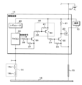
図2は駆動装置11の回路図である。駆動装置11は、MOSFET20に加えて、回路抵抗21、第1スイッチ22、第1スイッチ抵抗23,24、切替え回路25、第2スイッチ26、第2スイッチ抵抗27,28、レギュレータ29及びマイクロコンピュータ(以下、マイコン)30を有する。切替え回路25は、第3スイッチ40及び第3スイッチ抵抗41,42を有する。第1スイッチ22及び第2スイッチ26それぞれは、NPN型のバイポーラトランジスタである。第3スイッチ40はPNP型のバイポーラトランジスタである。
<Configuration of drive device 11>
FIG. 2 is a circuit diagram of the driving device 11. As shown in FIG. In addition to the MOSFET 20, the driving device 11 includes a circuit resistor 21, a first switch 22, first switch resistors 23 and 24, a switching circuit 25, a second switch 26, second switch resistors 27 and 28, a regulator 29 and a microcomputer ( (hereinafter referred to as a microcomputer) 30. The switching circuit 25 has a third switch 40 and third switch resistors 41 and 42 . Each of the first switch 22 and the second switch 26 is an NPN bipolar transistor. The third switch 40 is a PNP bipolar transistor.

MOSFET20のドレインは負荷13の他端に接続されている。MOSFET20のソースは第2導線15を介してグランド導体16に接続されている。回路抵抗21の一端は、直流電源10の正極に接続されている。回路抵抗21の他端はMOSFET20のゲートに接続されている。MOSFET20のゲートは、更に、第1スイッチ22のコレクタに接続されている。第1スイッチ22のエミッタは、MOSFET20のソースと、第2導線15の一端とに接続されている。第1スイッチ22のベース及びエミッタ間に第1スイッチ抵抗23が接続されている。第1スイッチ抵抗23は第2の抵抗として機能する。第1スイッチ22のベースは、更に、第1スイッチ抵抗24の一端に接続されている。 The drain of MOSFET 20 is connected to the other end of load 13 . The source of MOSFET 20 is connected to ground conductor 16 via second conductor 15 . One end of the circuit resistor 21 is connected to the positive electrode of the DC power supply 10 . The other end of circuit resistor 21 is connected to the gate of MOSFET 20 . The gate of MOSFET 20 is also connected to the collector of first switch 22 . The emitter of first switch 22 is connected to the source of MOSFET 20 and one end of second conductor 15 . A first switch resistor 23 is connected between the base and emitter of the first switch 22 . The first switch resistor 23 functions as a second resistor. The base of the first switch 22 is also connected to one end of the first switch resistor 24 .

直流電源10の正極は、切替え回路25が有する第3スイッチ40のエミッタに接続されている。第3スイッチ40のコレクタは第1スイッチ抵抗24の他端に接続されている。切替え回路25内では、第3スイッチ40のベース及びエミッタ間に第3スイッチ抵抗41が接続されている。第3スイッチ抵抗41は第3の抵抗として機能する。第3スイッチ40のベースは、更に、第3スイッチ抵抗42の一端に接続されている。 The positive electrode of the DC power supply 10 is connected to the emitter of the third switch 40 of the switching circuit 25 . A collector of the third switch 40 is connected to the other end of the first switch resistor 24 . A third switch resistor 41 is connected between the base and emitter of the third switch 40 in the switching circuit 25 . The third switch resistor 41 functions as a third resistor. The base of the third switch 40 is also connected to one end of a third switch resistor 42 .

第3スイッチ抵抗42の他端は、第2スイッチ26のコレクタに接続されている。第2スイッチ26のエミッタは第1導線14の一端に接続されている。第2スイッチ26のベース及びエミッタ間に第2スイッチ抵抗27が接続されている。第2スイッチ26のベースは、更に、第2スイッチ抵抗28の一端に接続されている。第2スイッチ抵抗28の他端はマイコン30に接続されている。
直流電源10の正極はレギュレータ29に接続されている。レギュレータ29は、更にマイコン30に接続されている。マイコン30は、更に、第1導線14の一端に接続されている。
The other end of the third switch resistor 42 is connected to the collector of the second switch 26 . The emitter of the second switch 26 is connected to one end of the first conductor 14 . A second switch resistor 27 is connected between the base and emitter of the second switch 26 . The base of the second switch 26 is also connected to one end of a second switch resistor 28 . The other end of the second switch resistor 28 is connected to the microcomputer 30 .
A positive electrode of the DC power supply 10 is connected to the regulator 29 . The regulator 29 is also connected to the microcomputer 30 . The microcomputer 30 is also connected to one end of the first conductor 14 .

以上のように、MOSFET20のゲート及びソース間に第1スイッチ22が接続されている。第2スイッチ26のエミッタは、第1導線14を介してグランド導体16に接続されている。第2スイッチのエミッタ、及び、第1導線14間の接続ノードには、複数の電気機器12が接続されている。第3スイッチ40のコレクタは、第1スイッチ抵抗24を介して第1スイッチ22のベースに接続されている。第3スイッチ40のベースは第3スイッチ抵抗42を介して第2スイッチ26のコレクタに接続されている。 As described above, the first switch 22 is connected between the gate and source of the MOSFET 20 . The emitter of second switch 26 is connected to ground conductor 16 via first conductor 14 . A plurality of electrical devices 12 are connected to the connection node between the emitter of the second switch and the first conductor 14 . The collector of third switch 40 is connected to the base of first switch 22 through first switch resistor 24 . The base of third switch 40 is connected to the collector of second switch 26 through third switch resistor 42 .

<駆動装置11の動作>
MOSFET20において、ソースの電位を基準としたゲートの電圧がゲート閾値以上である場合、ドレイン及びソース間の抵抗値が十分に小さい。このとき、MOSFET20はオンであり、ドレイン及びソースを介して電流が流れることが可能である。MOSFET20において、ソースの電位を基準としたゲートの電圧がゲート閾値未満である場合、ドレイン及びソース間の抵抗値が十分に大きい。このとき、MOSFET20はオフであり、ドレイン及びソースを介して電流が流れることはない。ゲート閾値は、正の一定値であり、予め設定されている。
<Operation of drive device 11>
In the MOSFET 20, when the voltage of the gate based on the potential of the source is equal to or higher than the gate threshold, the resistance value between the drain and the source is sufficiently small. At this time, MOSFET 20 is on and current can flow through its drain and source. In MOSFET 20, if the voltage of the gate with respect to the potential of the source is less than the gate threshold, the resistance between the drain and the source is sufficiently large. At this time, MOSFET 20 is off and no current flows through its drain and source. The gate threshold is a positive constant value and is preset.

第1スイッチ22において、エミッタの電位を基準としたベースの電圧が第1電圧閾値以上である場合、コレクタ及びエミッタ間の抵抗値が十分に小さい。このとき、第1スイッチ22はオンであり、コレクタ及びエミッタを介して電流が流れることが可能である。第1スイッチ22において、エミッタの電位を基準としたベースの電圧が第1電圧閾値未満である場合、コレクタ及びエミッタ間の抵抗値が十分に大きい。このとき、第1スイッチ22はオフであり、コレクタ及びエミッタを介して電流が流れることはない。第1電圧閾値は、正の一定値であり、予め設定されている。第1電圧閾値は第2の閾値に相当する。 In the first switch 22, if the voltage of the base with respect to the potential of the emitter is greater than or equal to the first voltage threshold, the resistance between the collector and the emitter is sufficiently small. At this time, the first switch 22 is on and current can flow through the collector and emitter. In the first switch 22, if the voltage of the base relative to the potential of the emitter is less than the first voltage threshold, the resistance between the collector and the emitter is sufficiently high. At this time, the first switch 22 is off and no current flows through the collector and emitter. The first voltage threshold is a constant positive value and is preset. The first voltage threshold corresponds to the second threshold.

第2スイッチ26は、第1スイッチ22と同様に構成されている。第2スイッチ26において、エミッタの電位を基準としたベースの電圧が第2電圧閾値以上である場合、第2スイッチ26はオンである。第2スイッチ26において、エミッタの電位を基準としたベースの電圧が第2電圧閾値未満である場合、第2スイッチ26はオフである。第2電圧閾値は、正の一定値であり、予め設定されている。 The second switch 26 is configured similarly to the first switch 22 . If the voltage of the base relative to the potential of the emitter in the second switch 26 is greater than or equal to the second voltage threshold, then the second switch 26 is on. If the voltage of the base relative to the potential of the emitter in the second switch 26 is less than a second voltage threshold, the second switch 26 is off. The second voltage threshold is a constant positive value and is preset.

第3スイッチ40において、エミッタの電位を基準としたベースの電圧が第3電圧閾値未満である場合、エミッタ及びコレクタ間の抵抗値が十分に小さい。このとき、第3スイッチ40はオンであり、エミッタ及びコレクタを介して電流が流れることが可能である。第3スイッチ40において、エミッタの電位を基準としたベースの電圧が第3電圧閾値以上である場合、エミッタ及びコレクタ間の抵抗値が十分に大きい。このとき、第3スイッチ40はオフであり、エミッタ及びコレクタを介して電流が流れることはない。第3電圧閾値は、負の一定値であり、予め設定されている。第3電圧閾値は第3の閾値に相当する。 In the third switch 40, the resistance between the emitter and collector is sufficiently small if the voltage of the base relative to the potential of the emitter is less than the third voltage threshold. At this time, the third switch 40 is on and current can flow through the emitter and collector. In the third switch 40, if the voltage of the base with respect to the potential of the emitter is equal to or higher than the third voltage threshold, the resistance between the emitter and collector is sufficiently large. At this time, the third switch 40 is off and no current flows through the emitter and collector. The third voltage threshold is a constant negative value and is preset. The third voltage threshold corresponds to the third threshold.

以下では、グランド導体16の電位を基準とした直流電源10の電圧を電源電圧と記載する。レギュレータ29は、電源電圧を目標電圧に降圧し、目標電圧をマイコン30に印加する。これにより、マイコン30に電力が供給される。電源電圧は、例えば12Vである。目標電圧は例えば5Vである。マイコン30に電力が供給されている場合、電流は、直流電源10の正極から、レギュレータ29、マイコン30、第1導線14及びグランド導体16の順に流れる。 Hereinafter, the voltage of the DC power supply 10 based on the potential of the ground conductor 16 is referred to as power supply voltage. The regulator 29 steps down the power supply voltage to the target voltage and applies the target voltage to the microcomputer 30 . Thereby, power is supplied to the microcomputer 30 . The power supply voltage is, for example, 12V. The target voltage is, for example, 5V. When power is supplied to the microcomputer 30 , current flows from the positive electrode of the DC power supply 10 through the regulator 29 , the microcomputer 30 , the first conductor 14 and the ground conductor 16 in this order.

マイコン30は、ハイレベル電圧及びローレベル電圧によって構成される制御信号を、第2スイッチ抵抗28を介して、第2スイッチ26の制御端に出力する。ハイレベル電圧及びローレベル電圧それぞれは、第2スイッチ26のエミッタの電位とした電圧である。ハイレベル電圧はローレベル電圧よりも高い。ローレベル電圧は例えばゼロVである。マイコン30は、制御信号の電圧を切替えることによってMOSFET20をオン又はオフに切替える。マイコン30は出力部として機能する。 The microcomputer 30 outputs a control signal composed of high-level voltage and low-level voltage to the control end of the second switch 26 via the second switch resistor 28 . Each of the high-level voltage and the low-level voltage is the potential of the emitter of the second switch 26 . The high level voltage is higher than the low level voltage. A low level voltage is, for example, zero volts. The microcomputer 30 switches the MOSFET 20 on or off by switching the voltage of the control signal. The microcomputer 30 functions as an output section.

前述したように、複数の電気機器の作動又は動作の停止によって、第1導線14を流れる電流は変動する。第1導線14を流れる電流が変動した場合、第2スイッチ26のエミッタの電位、即ち、グランド導体16の電位を基準とした第1導線14の一端の電圧は変動する。
なお、前述したように、ノイズに係る電流が第1導線14を流れるか、又は、グランド導体16における第1導線14の接触抵抗が増加した場合も、第1導線14を流れる電流が変動し、グランド導体16の電位を基準とした第1導線14の一端の電圧は変動する。
As described above, the current flowing through the first conductor 14 fluctuates due to the activation or deactivation of a plurality of electrical devices. When the current flowing through the first conductor 14 fluctuates, the potential of the emitter of the second switch 26, that is, the voltage at one end of the first conductor 14 relative to the potential of the ground conductor 16 fluctuates.
In addition, as described above, when a current related to noise flows through the first conducting wire 14 or when the contact resistance of the first conducting wire 14 in the ground conductor 16 increases, the current flowing through the first conducting wire 14 also fluctuates, The voltage at one end of the first conductor 14 relative to the potential of the ground conductor 16 fluctuates.

図3は、MOSFET20の切替えを説明するためのタイミングチャートである。図3では、ハイレベル電圧が「H」で示され、ローレベル電圧が「L」で示されている。制御信号の電圧の推移と、第2スイッチ26、第3スイッチ40、第1スイッチ22及びMOSFET20の状態の推移とが示されている。これらの推移について横軸には時間が示されている。 FIG. 3 is a timing chart for explaining switching of the MOSFET 20. As shown in FIG. In FIG. 3, the high level voltage is indicated by "H" and the low level voltage is indicated by "L". Changes in the voltage of the control signal and changes in the states of the second switch 26, the third switch 40, the first switch 22 and the MOSFET 20 are shown. Time is shown on the horizontal axis for these transitions.

制御信号の電圧がゼロVを超えている場合、電流は、マイコン30から第2スイッチ抵抗28,27の順に流れ、マイコン30に戻る。マイコン30は、負荷13を駆動する場合、制御信号の電圧をハイレベル電圧からローレベル電圧に切替える。制御信号の電圧がローレベル電圧である場合、第2スイッチ抵抗を流れる電流は、十分に小さいか、又は、ゼロAである。このため、第2スイッチ26において、エミッタの電位を基準としたベースの電圧は、十分に低いか、又は、ゼロVであり、第2電圧閾値未満である。このため、第2スイッチ26はオフである。 When the voltage of the control signal exceeds zero volts, current flows from the microcomputer 30 through the second switch resistors 28 and 27 and back to the microcomputer 30 . When the microcomputer 30 drives the load 13, it switches the voltage of the control signal from the high level voltage to the low level voltage. When the voltage of the control signal is a low level voltage, the current through the second switch resistor is sufficiently small or zero amperes. Thus, in the second switch 26, the voltage of the base relative to the potential of the emitter is sufficiently low or zero volts and below the second voltage threshold . Therefore, the second switch 26 is off.

第2スイッチ26がオフである場合、第3スイッチ抵抗41,42を電流が流れることはない。このため、第3スイッチ40において、エミッタの電位を基準としたベースの電圧は、ゼロVであり、第3電圧閾値以上である。このため、第3スイッチ40はオフである。 When the second switch 26 is off, no current flows through the third switch resistors 41,42. Therefore, in the third switch 40, the voltage of the base relative to the potential of the emitter is zero volts, which is greater than or equal to the third voltage threshold. Therefore, the third switch 40 is off.

第3スイッチ40がオフである場合、第1スイッチ抵抗23,24を電流が流れることはない。このため、第1スイッチ22において、エミッタの電位を基準としたベースの電圧は、ゼロVであり、第1電圧閾値未満である。このため、第1スイッチ22はオフである。従って、切替え回路25は、第2スイッチ26がオフに切替わった場合、第1スイッチ22をオフに切替える。 When the third switch 40 is off, no current flows through the first switch resistors 23,24. Thus, in the first switch 22, the voltage of the base relative to the potential of the emitter is zero volts, which is less than the first voltage threshold. Therefore, the first switch 22 is off. Therefore, the switching circuit 25 switches off the first switch 22 when the second switch 26 is switched off.

第1スイッチ22がオフである場合、回路抵抗21に電流が流れないので、グランド導体16の電位を基準としたゲートの電圧は、電源電圧である。ノイズに係る電流が第2導線15を流れるか、又は、グランド導体16において第2導線15の接触抵抗が増加した場合、グランド導体16の電位を基準とした第2導線15の一端、即ち、MOSFET20のソースの電圧は変動する。電源電圧は、グランド導体16の電位を基準としたMOSFET20のソースの電圧の最大値よりも十分に大きい。この最大値と電源電圧との差はゲート閾値以上である。このため、第1スイッチ22がオフである場合、MOSFET20において、ソースの電位を基準としたゲートの電圧は、ゲート閾値以上であり、MOSFET20はオンである。 When the first switch 22 is off, no current flows through the circuit resistor 21, so the voltage of the gate relative to the potential of the ground conductor 16 is the power supply voltage. When a current associated with noise flows through the second conducting wire 15 or the contact resistance of the second conducting wire 15 increases in the ground conductor 16, one end of the second conducting wire 15 with reference to the potential of the ground conductor 16, that is, the MOSFET 20 , the voltage at the source varies. The power supply voltage is well above the maximum voltage at the source of MOSFET 20 relative to the potential of ground conductor 16 . The difference between this maximum value and the power supply voltage is greater than or equal to the gate threshold. Therefore, when the first switch 22 is off, the voltage of the gate with respect to the potential of the source in the MOSFET 20 is equal to or higher than the gate threshold, and the MOSFET 20 is on.

MOSFET20がオンである場合、電流は、直流電源10の正極から負荷13、MOSFET20、第2導線15及びグランド導体16の順に流れ、直流電源10の負極に戻る。これにより、負荷13に電力が供給され、負荷13が作動する。このとき、MOSFET20のドレインに電流が入力され、MOSFET20のソースから電流が出力される。 When MOSFET 20 is on, current flows from the positive terminal of DC power supply 10 through load 13 , MOSFET 20 , second conductor 15 , ground conductor 16 and back to the negative terminal of DC power supply 10 . Thereby, power is supplied to the load 13 and the load 13 operates. At this time, current is input to the drain of the MOSFET 20 and current is output from the source of the MOSFET 20 .

直流電源10の正極から負荷13、MOSFET20、第2導線15及びグランド導体16の順に流れる電流の電流経路は、負荷13を介して流れる電流の電流経路である。MOSFET20は、この電流経路における負荷13の下流側に配置されている。 A current path of current flowing from the positive electrode of the DC power supply 10 to the load 13 , the MOSFET 20 , the second conductor 15 and the ground conductor 16 in this order is a current path of current flowing through the load 13 . The MOSFET 20 is arranged downstream of the load 13 in this current path.

マイコン30は、負荷13の動作を停止させる場合、制御信号の電圧をローレベル電圧からハイレベル電圧に切替える。制御信号の電圧がハイレベル電圧である場合、第2スイッチ抵抗28,27の順に流れる電流は十分に大きい。このため、制御信号の電圧がハイレベル電圧である場合、第2スイッチ26において、エミッタの電位を基準としたベースの電圧は、第2電圧閾値以上であり、第2スイッチ26はオンである。 When stopping the operation of the load 13, the microcomputer 30 switches the voltage of the control signal from the low level voltage to the high level voltage. When the voltage of the control signal is a high level voltage, the currents flowing through the second switch resistors 28 and 27 are sufficiently large. Therefore, when the voltage of the control signal is a high-level voltage, the voltage of the base of the second switch 26 with respect to the potential of the emitter is equal to or higher than the second voltage threshold, and the second switch 26 is on.

第2スイッチ26がオンである場合、電流は、直流電源10の正極から、第3スイッチ抵抗41,42、第2スイッチ26、第1導線14及びグランド導体16の順に流れ、直流電源10の負極に戻る。これにより、第3スイッチ抵抗41において電圧降下が生じ、第3スイッチ40において、エミッタの電位を基準としたベースの電圧は第3電圧閾値未満である。結果、第2スイッチ26がオンである場合、第3スイッチ40はオンである。 When the second switch 26 is on, current flows from the positive electrode of the DC power supply 10 through the third switch resistors 41 and 42, the second switch 26, the first conductor 14 and the ground conductor 16 in this order, and the negative electrode of the DC power supply 10. back to This causes a voltage drop across the third switch resistor 41 and in the third switch 40 the voltage at the base relative to the potential at the emitter is below the third voltage threshold. As a result, when the second switch 26 is on, the third switch 40 is on.

第2スイッチ26がオンである場合、第2スイッチ26のコレクタに電流が入力され、第2スイッチ26のエミッタから電流が出力される。第2スイッチ26について、コレクタ、エミッタ及びベースそれぞれは、入力端、出力端及び制御端として機能する。 When the second switch 26 is on, current is input to the collector of the second switch 26 and current is output from the emitter of the second switch 26 . For the second switch 26, the collector, emitter and base act as input, output and control, respectively.

第3スイッチ40がオンである場合、電流は、直流電源10の正極から、第3スイッチ40、第1スイッチ抵抗24,23、第2導線15及びグランド導体16の順に流れ、直流電源10の負極に戻る。これにより、第1スイッチ抵抗23において電圧降下が生じ、第1スイッチ22において、エミッタの電位を基準としたベースの電圧は第1電圧閾値以上である。結果、第3スイッチ40がオンである場合、第1スイッチ22はオンである。切替え回路25は、第2スイッチ26がオンに切替わった場合、第1スイッチ22をオンに切替える。 When the third switch 40 is on, the current flows from the positive electrode of the DC power supply 10 to the third switch 40, the first switch resistors 24 and 23, the second conductor 15 and the ground conductor 16 in this order, and then the negative electrode of the DC power supply 10. back to This causes a voltage drop across the first switch resistor 23, and in the first switch 22, the voltage of the base with respect to the potential of the emitter is greater than or equal to the first voltage threshold. As a result, when the third switch 40 is on, the first switch 22 is on. The switching circuit 25 turns on the first switch 22 when the second switch 26 is turned on.

前述したように、電源電圧は、グランド導体16の電位を基準としたMOSFET20のソース、即ち、第1スイッチ22のエミッタの電圧の最大値よりも十分に大きい。このため、第1スイッチ抵抗23を流れる電流は大きく、第1スイッチ抵抗23における電圧降下の幅は第1電圧閾値以上である。従って、第3スイッチ40がオンである場合、第1スイッチ22は確実にオンに切替わる。 As previously mentioned, the power supply voltage is sufficiently greater than the maximum voltage at the source of MOSFET 20 , ie the emitter of first switch 22 , relative to the potential of ground conductor 16 . Therefore, the current flowing through the first switch resistor 23 is large, and the width of the voltage drop across the first switch resistor 23 is greater than or equal to the first voltage threshold. Therefore, when the third switch 40 is on, the first switch 22 is reliably switched on.

第3スイッチ40がオンである場合、第3スイッチ40のエミッタに電流が入力され、第3スイッチ40のコレクタから電流が出力される。第3スイッチ40について、エミッタ、コレクタ及びベースそれぞれは、入力端、出力端及び制御端として機能する。 When the third switch 40 is on, current is input to the emitter of the third switch 40 and current is output from the collector of the third switch 40 . For the third switch 40, the emitter, collector and base function as input, output and control, respectively.

第1スイッチ22がオンである場合、MOSFET20において、ソースの電位を基準としたゲートの電圧は、ゼロVであり、ゲート閾値未満である。従って、第1スイッチ22がオンである場合、MOSFET20はオフである。 When the first switch 22 is on, the voltage at the gate relative to the potential at the source in MOSFET 20 is zero volts, below the gate threshold. Thus, when first switch 22 is on, MOSFET 20 is off.

以上のように、制御信号の電圧がローレベル電圧である場合、即ち、マイコン30がローレベル電圧を第2スイッチ26のゲートに出力している場合、MOSFET20はオンである。制御信号の電圧がハイレベル電圧である場合、即ち、マイコン30がハイレベル電圧を第2スイッチ26のゲートに出力している場合、MOSFET20はオフである。 As described above, when the voltage of the control signal is a low level voltage, that is, when the microcomputer 30 outputs a low level voltage to the gate of the second switch 26, the MOSFET 20 is on. When the voltage of the control signal is a high level voltage, that is, when the microcomputer 30 outputs a high level voltage to the gate of the second switch 26, the MOSFET 20 is off.

第1スイッチ22がオンである場合、電流は、直流電源10の正極から回路抵抗21、第1スイッチ22、第2導線15及びグランド導体16の順に流れ、直流電源10の負極に戻る。第1スイッチ22がオンである場合、第1スイッチ22のコレクタに電流が入力され、第1スイッチ22のエミッタから電流が出力される。第1スイッチ22について、コレクタ、エミッタ及びベースそれぞれは、入力端、出力端及び制御端として機能する。 When the first switch 22 is on, current flows from the positive terminal of the DC power supply 10 through the circuit resistor 21, the first switch 22, the second conductor 15 and the ground conductor 16 in this order, and returns to the negative terminal of the DC power supply 10. When the first switch 22 is on, current is input to the collector of the first switch 22 and current is output from the emitter of the first switch 22 . For the first switch 22, the collector, emitter and base act as input, output and control, respectively.

第1導線14が断線した場合、又は、第1導線14を介した駆動装置11とグランド導体16との接続が外れた場合、第2スイッチ26のエミッタが開放される。この場合、第2スイッチ抵抗27に電流が流れないので、第2スイッチ26において、エミッタの電位を基準としたベースの電圧は、ゼロVであり、第2電圧閾値未満である。このとき、第2スイッチ26はオフである。前述したように、第2スイッチ26がオフである場合、第3スイッチ40及び第1スイッチ22はオフであり、MOSFET20はオンである。従って、第2スイッチ26のエミッタが開放された場合、MOSFET20はオンに維持される。 The emitter of the second switch 26 is opened when the first conductor 14 is broken, or when the connection between the driving device 11 and the ground conductor 16 via the first conductor 14 is broken. In this case, since no current flows through the second switch resistor 27, the voltage of the base relative to the potential of the emitter of the second switch 26 is zero V, which is less than the second voltage threshold. At this time, the second switch 26 is off. As previously mentioned, when second switch 26 is off, third switch 40 and first switch 22 are off and MOSFET 20 is on. Thus, when the emitter of second switch 26 is open, MOSFET 20 remains on.

<駆動装置11の効果>
マイコン30が第2スイッチ26に出力するハイレベル電圧及びローレベル電圧は、第2スイッチ26のエミッタの電位を基準とした電圧である。第2スイッチ26は、エミッタの電位を基準としたベースの電圧に応じてオン又はオフに切替わる。このため、ハイレベル電圧及びローレベル電圧の基準電位、即ち、グランド導体16の電位を基準とした第2スイッチ26のエミッタの電圧が変動した場合であっても、第2スイッチ26は誤りなくオン又はオフに切替わる。
<Effects of drive device 11>
The high-level voltage and low-level voltage that the microcomputer 30 outputs to the second switch 26 are voltages based on the potential of the emitter of the second switch 26 . The second switch 26 switches on or off depending on the voltage of the base relative to the potential of the emitter. Therefore, even if the voltage of the emitter of the second switch 26 based on the reference potential of the high-level voltage and the low-level voltage, that is, the potential of the ground conductor 16, fluctuates, the second switch 26 is turned on without error. or switched off.

また、直流電源10の電源電圧は、グランド導体16の電位を基準とした第1導線14の一端の電圧の最大値よりも十分に高い。このため、第2スイッチ26がオンである場合、第3スイッチ抵抗41を十分に大きな電流が流れ、第3スイッチ40において、エミッタの電位を基準としたベースの電圧は第3電圧閾値未満である。結果、第2スイッチ26がオンに切替わった場合、グランド導体16の電位を基準とした第1導線14の一端の電圧に無関係に、第3スイッチ40がオンに切替わる。前述したように、第3スイッチ40がオンに切替わった場合、第1スイッチ22がオンに切替わり、MOSFET20がオフに切替わる。 Also, the power supply voltage of the DC power supply 10 is sufficiently higher than the maximum value of the voltage at one end of the first conductor 14 with the potential of the ground conductor 16 as a reference. Thus, when the second switch 26 is on, a sufficiently large current flows through the third switch resistor 41 such that in the third switch 40 the voltage at the base relative to the potential at the emitter is less than the third voltage threshold. . As a result, when the second switch 26 is turned on, the third switch 40 is turned on regardless of the voltage at one end of the first conductor 14 relative to the potential of the ground conductor 16 . As mentioned above, when the third switch 40 is turned on, the first switch 22 is turned on and the MOSFET 20 is turned off.

第2スイッチ26がオフに切替わった場合、グランド導体16の電位を基準とした第1導線14の一端の電圧に無関係に、第3スイッチ抵抗41を介して電流の通流は停止し、第3スイッチ40はオフに切替わる。前述したように、第3スイッチ40がオフに切替わった場合、第1スイッチ22はオフに切替わり、MOSFET20はオンに切替わる。
以上のように、第2スイッチ26の切替えに誤りがない場合、MOSFET20の切替えも誤りなく行われる。結果、制御信号の電圧の基準電位、即ち、グランド導体16の電位を基準とした第1導線14の一端の電圧が変動した場合であっても、MOSFET20は誤りなくオン又はオフに切替わる。
When the second switch 26 is switched off, regardless of the voltage at one end of the first conductor 14 relative to the potential of the ground conductor 16, the current stops flowing through the third switch resistor 41 and the second switch 26 is turned off. 3 Switch 40 is switched off. As mentioned above, when the third switch 40 is turned off, the first switch 22 is turned off and the MOSFET 20 is turned on.
As described above, when there is no error in switching the second switch 26, the switching of the MOSFET 20 is also performed without error. As a result, even if the voltage at one end of the first conductor 14 relative to the reference potential of the control signal voltage, that is, the potential of the ground conductor 16, fluctuates, the MOSFET 20 is switched on or off without error.

<なお書き>
MOSFET20は、電流が出力される出力端の電位を基準とした制御端の電圧を上昇させることによってオンに切替わるスイッチであればよい。このため、MOSFET20の代わりに、MOSFETとは異なるNチャネル型のFET、IGBT(Insulated Gate Bipolar Transistor)又は、NPN型のバイポーラトランジスタ等を用いてもよい。
<note>
The MOSFET 20 may be a switch that is turned on by increasing the voltage at the control end based on the potential at the output end to which the current is output. Therefore, instead of the MOSFET 20, an N-channel FET, an IGBT (Insulated Gate Bipolar Transistor), an NPN bipolar transistor, or the like, which is different from the MOSFET, may be used.

(実施形態2)
実施形態1においては、負荷13の電力供給の制御に用いるスイッチの数は、1つである。しかしながら、負荷13の電力供給の制御に用いるスイッチの数は、1に限定されず、2以上であってもよい。
以下では、実施形態2について、実施形態1と異なる点を説明する。後述する構成を除く他の構成は、実施形態1と共通している。このため、実施形態1と共通する構成部には実施形態1と同一の参照符号を付してその説明を省略する。
(Embodiment 2)
In Embodiment 1, the number of switches used for controlling power supply to the load 13 is one. However, the number of switches used for controlling power supply to the load 13 is not limited to one, and may be two or more.
Below, the points of the second embodiment that are different from the first embodiment will be described. Configurations other than those described later are common to the first embodiment. For this reason, the same reference numerals as those of the first embodiment are given to the components that are common to the first embodiment, and the description thereof is omitted.

<駆動装置11の概要>
図4は、実施形態2における駆動装置11の要部構成を示すブロック図である。実施形態2における電源システム1では、駆動装置11は、負荷13として、モータMを駆動する。実施形態2における電源システム1は、実施形態1と同様に、電気機器12を有していなくてもよい。駆動装置11は、第1上流スイッチ50u、第1下流スイッチ50d、第2上流スイッチ51u及び第2下流スイッチ51dを有する。直流電源10の正極からモータMを介して流れる電流の電流経路として、第1電流経路及び第2電流経路が設けられている。
<Outline of drive device 11>
FIG. 4 is a block diagram showing the main configuration of the driving device 11 according to the second embodiment. In the power supply system 1 according to the second embodiment, the driving device 11 drives the motor M as the load 13 . The power supply system 1 according to the second embodiment may not have the electrical equipment 12 as in the first embodiment. The driving device 11 has a first upstream switch 50u, a first downstream switch 50d, a second upstream switch 51u and a second downstream switch 51d. A first current path and a second current path are provided as current paths for current flowing from the positive electrode of the DC power supply 10 through the motor M. As shown in FIG.

第1電流経路において、モータMの上流側及び下流側それぞれに第1上流スイッチ50u及び第1下流スイッチ50dが配置されている。第2電流経路において、モータMの上流側及び下流側それぞれに第2上流スイッチ51u及び第2下流スイッチ51dが配置されている。第1電流経路を電流が流れている場合にモータMを流れる電流の方向は、第1方向であり、図4においては下向きである。第2電流経路を電流が流れている場合にモータMを流れる電流の方向は、第2方向であり、図4において上向きである。第1方向は第2方向と異なる。 A first upstream switch 50u and a first downstream switch 50d are arranged upstream and downstream of the motor M in the first current path, respectively. A second upstream switch 51u and a second downstream switch 51d are arranged upstream and downstream of the motor M in the second current path, respectively. The direction of the current flowing through the motor M when the current is flowing through the first current path is the first direction, which is downward in FIG. The direction of the current flowing through the motor M when the current is flowing through the second current path is the second direction, which is upward in FIG. The first direction is different than the second direction.

駆動装置11は、第2上流スイッチ51u及び第2下流スイッチ51dがオフである状態で第1上流スイッチ50u及び第1下流スイッチ50dをオンに切替える。これにより、第1方向の電流がモータMに流れ、モータMは正方向に回転する。モータMは円柱状のロータを有する。モータMの回転は、ロータの軸回りの回転を意味する。正方向は例えば時計回りの方向である。 The driving device 11 switches on the first upstream switch 50u and the first downstream switch 50d while the second upstream switch 51u and the second downstream switch 51d are off. As a result, the current in the first direction flows through the motor M, and the motor M rotates in the forward direction. The motor M has a cylindrical rotor. Rotation of the motor M means rotation of the rotor about its axis. The positive direction is, for example, the clockwise direction.

駆動装置11は、第1上流スイッチ50u及び第1下流スイッチ50dがオフである状態で第2上流スイッチ51u及び第2下流スイッチ51dをオンに切替える。これにより、第2方向の電流がモータMに流れ、モータMは逆方向に回転する。正方向が時計回りである場合、逆方向は反時計回りの方向である。
モータMは、例えば、車両の窓を開閉するために用いられる。モータMが正方向に回転した場合、例えば、車両の窓が開放される。モータMが逆方向に回転した場合、例えば、車両の窓が閉鎖される。
The driving device 11 turns on the second upstream switch 51u and the second downstream switch 51d while the first upstream switch 50u and the first downstream switch 50d are turned off. This causes current in the second direction to flow through the motor M, causing the motor M to rotate in the opposite direction. If the positive direction is clockwise, the reverse direction is the counterclockwise direction.
Motor M is used, for example, to open and close windows of a vehicle. When the motor M rotates in the forward direction, for example, the windows of the vehicle are opened. If the motor M rotates in the opposite direction, for example, the windows of the vehicle are closed.

駆動装置11は、第1上流スイッチ50u及び第2上流スイッチ51uをオフに切替える。これにより、直流電源10からモータMへの電力供給が停止し、モータMが動作を停止する。 The driving device 11 switches off the first upstream switch 50u and the second upstream switch 51u. As a result, the power supply from the DC power supply 10 to the motor M stops, and the motor M stops operating.

<駆動装置11の構成>
図4に示すように、駆動装置11は、第1上流スイッチ50u、第1下流スイッチ50d、第2上流スイッチ51u及び第2下流スイッチ51dに加えて、レギュレータ29、マイコン30、第1上流駆動回路52u、第1下流駆動回路52d、第2上流駆動回路53u、第2下流駆動回路53d及びスイッチ抵抗54,55を有する。第1上流スイッチ50u、第1下流スイッチ50d、第2上流スイッチ51u及び第2下流スイッチ51dそれぞれは、Nチャネル型のMOSFETである。
<Configuration of drive device 11>
As shown in FIG. 4, the driving device 11 includes a first upstream switch 50u, a first downstream switch 50d, a second upstream switch 51u, and a second downstream switch 51d, as well as a regulator 29, a microcomputer 30, and a first upstream driving circuit. 52u, a first downstream drive circuit 52d, a second upstream drive circuit 53u, a second downstream drive circuit 53d, and switch resistors 54 and 55. Each of the first upstream switch 50u, the first downstream switch 50d, the second upstream switch 51u, and the second downstream switch 51d is an N-channel MOSFET.

直流電源10、レギュレータ29、マイコン30、第1導線14及びグランド導体16は実施形態1と同様に接続されている。第1導線14の一端には、複数の電気機器12が接続されている。第1上流スイッチ50uのドレインは、直流電源10の正極に接続されている。第1上流スイッチ50uのソースは、モータMの一端に接続されている。モータMの他端は、第1下流スイッチ50dのドレインに接続されている。第1下流スイッチ50dのソースは、第2導線15を介してグランド導体16に接続されている。第1下流スイッチ50dのゲート及びソース間には、スイッチ抵抗54が接続されている。 A DC power supply 10, a regulator 29, a microcomputer 30, a first conductor 14 and a ground conductor 16 are connected in the same manner as in the first embodiment. A plurality of electric devices 12 are connected to one end of the first conducting wire 14 . A drain of the first upstream switch 50 u is connected to the positive electrode of the DC power supply 10 . The source of the first upstream switch 50u is connected to one end of the motor M. The other end of the motor M is connected to the drain of the first downstream switch 50d. A source of the first downstream switch 50 d is connected to the ground conductor 16 via the second conductor 15 . A switch resistor 54 is connected between the gate and source of the first downstream switch 50d.

第2上流スイッチ51uのドレインは、直流電源10の正極に接続されている。第2上流スイッチ51uのソースは、第1下流スイッチ50d及びモータM間の接続ノードに接続されている。第1上流スイッチ50u及びモータM間の接続ノードは、第2下流スイッチ51dのドレインに接続されている。第2下流スイッチ51dのソースは、第2導線15を介してグランド導体16に接続されている。第2下流スイッチ51dのゲート及びソース間には、スイッチ抵抗55が接続されている。 A drain of the second upstream switch 51 u is connected to the positive electrode of the DC power supply 10 . The source of the second upstream switch 51u is connected to the connection node between the first downstream switch 50d and the motor M. A connection node between the first upstream switch 50u and the motor M is connected to the drain of the second downstream switch 51d. A source of the second downstream switch 51 d is connected to the ground conductor 16 via the second conductor 15 . A switch resistor 55 is connected between the gate and source of the second downstream switch 51d.

第1上流スイッチ50u、第1下流スイッチ50d、第2上流スイッチ51u及び第2下流スイッチ51dそれぞれのゲートは、第1上流駆動回路52u、第1下流駆動回路52d、第2上流駆動回路53u及び第2下流駆動回路53dに接続されている。第1上流駆動回路52uはマイコン30に接続されている。第1上流駆動回路52u及びマイコン30間の接続ノードは、第2下流駆動回路53dに接続されている。第2上流駆動回路53uはマイコン30に接続されている。第2上流駆動回路53u及びマイコン30間の接続ノードは、第1下流駆動回路52dに接続されている。 Gates of the first upstream switch 50u, the first downstream switch 50d, the second upstream switch 51u, and the second downstream switch 51d are connected to the first upstream drive circuit 52u, the first downstream drive circuit 52d, the second upstream drive circuit 53u, and the second upstream drive circuit 53u. 2 is connected to the downstream drive circuit 53d. The first upstream drive circuit 52 u is connected to the microcomputer 30 . A connection node between the first upstream drive circuit 52u and the microcomputer 30 is connected to the second downstream drive circuit 53d. The second upstream drive circuit 53 u is connected to the microcomputer 30 . A connection node between the second upstream drive circuit 53u and the microcomputer 30 is connected to the first downstream drive circuit 52d.

マイコン30は、更に、第1下流駆動回路52d及び第2下流駆動回路53dそれぞれに直接に接続されている。第1下流駆動回路52d及び第2下流駆動回路53dそれぞれは、マイコン30及び第1導線14間の接続ノードに接続されている。第1下流駆動回路52dは、更に、第1下流スイッチ50dのソースに接続されている。第2下流駆動回路53dは、更に、第2下流スイッチ51dのソースに接続されている。 The microcomputer 30 is further directly connected to each of the first downstream drive circuit 52d and the second downstream drive circuit 53d. The first downstream drive circuit 52d and the second downstream drive circuit 53d are connected to connection nodes between the microcomputer 30 and the first conductor 14, respectively. The first downstream drive circuit 52d is also connected to the source of the first downstream switch 50d. The second downstream drive circuit 53d is further connected to the source of the second downstream switch 51d.

第1下流駆動回路52d及び第2下流駆動回路53dそれぞれは、直流電源10の正極に接続されている。図面が煩雑になることを防ぐため、これらの接続線の記載を図4では省略している。 The first downstream drive circuit 52 d and the second downstream drive circuit 53 d are each connected to the positive electrode of the DC power supply 10 . In order to avoid complicating the drawing, the illustration of these connection lines is omitted in FIG.

<駆動装置11の動作>
第1上流スイッチ50u、第1下流スイッチ50d、第2上流スイッチ51u及び第2下流スイッチ51dそれぞれについて、ソースの電位を基準としたゲートの電圧がスイッチ閾値以上である場合、ドレイン及びソース間の抵抗値は十分に小さい。このとき、第1上流スイッチ50u、第1下流スイッチ50d、第2上流スイッチ51u及び第2下流スイッチ51dそれぞれはオンであり、ドレイン及びソースを介して電流が流れることが可能である。
<Operation of drive device 11>
For each of the first upstream switch 50u, the first downstream switch 50d, the second upstream switch 51u, and the second downstream switch 51d, when the voltage of the gate based on the potential of the source is equal to or higher than the switch threshold, the resistance between the drain and the source value is small enough. At this time, each of the first upstream switch 50u, the first downstream switch 50d, the second upstream switch 51u, and the second downstream switch 51d is on, and current can flow through the drain and the source.

第1上流スイッチ50u、第1下流スイッチ50d、第2上流スイッチ51u及び第2下流スイッチ51dそれぞれについて、ソースの電位を基準としたゲートの電圧がスイッチ閾値未満である場合、ドレイン及びソース間の抵抗値は十分に大きい。このとき、第1上流スイッチ50u、第1下流スイッチ50d、第2上流スイッチ51u及び第2下流スイッチ51dそれぞれはオフであり、ドレイン及びソースを介して電流が流れることはない。スイッチ閾値は、正の一定値であり、予め設定されている。第1上流スイッチ50u、第1下流スイッチ50d、第2上流スイッチ51u及び第2下流スイッチ51dのスイッチ閾値それぞれは、他のスイッチ閾値と同一であってもよいし、他のスイッチ閾値と異なっていてもよい。 For each of the first upstream switch 50u, the first downstream switch 50d, the second upstream switch 51u, and the second downstream switch 51d, when the voltage of the gate with respect to the potential of the source is less than the switch threshold, the resistance between the drain and the source value is large enough. At this time, the first upstream switch 50u, the first downstream switch 50d, the second upstream switch 51u, and the second downstream switch 51d are off, and no current flows through the drain and source. The switch threshold is a constant positive value and is preset. Each of the switch thresholds of the first upstream switch 50u, the first downstream switch 50d, the second upstream switch 51u, and the second downstream switch 51d may be the same as or different from the other switch thresholds. good too.

マイコン30は、第1上流駆動回路52u及び第2下流駆動回路53dに右側制御信号を出力する。マイコン30は、第2上流駆動回路53u及び第1下流駆動回路52dに左側制御信号を出力する。右側制御信号及び左側制御信号それぞれは、ハイレベル電圧及びローレベル電圧によって構成される。マイコン30は、右側制御信号及び左側制御信号の電圧それぞれをハイレベル電圧又はローレベル電圧に切替える。第1上流駆動回路52u及び第2下流駆動回路53dそれぞれは、右側制御信号の電圧に応じてオン又はオフに切替わる。第2上流駆動回路53u及び第1下流駆動回路52dそれぞれは、左側制御信号の電圧に応じてオン又はオフに切替わる。 The microcomputer 30 outputs right control signals to the first upstream drive circuit 52u and the second downstream drive circuit 53d. The microcomputer 30 outputs left control signals to the second upstream drive circuit 53u and the first downstream drive circuit 52d. Each of the right control signal and the left control signal is composed of a high level voltage and a low level voltage. The microcomputer 30 switches the voltage of each of the right control signal and the left control signal to a high level voltage or a low level voltage. Each of the first upstream drive circuit 52u and the second downstream drive circuit 53d is switched on or off according to the voltage of the right control signal. Each of the second upstream drive circuit 53u and the first downstream drive circuit 52d is switched on or off according to the voltage of the left control signal.

図5は、駆動装置11の動作を説明するためのタイミングチャートである。図5でも、ハイレベル電圧が「H」で示され、ローレベル電圧が「L」で示されている。右側制御信号及び左側制御信号の推移と、第1上流スイッチ50u、第1下流スイッチ50d、第2上流スイッチ51u及び第2下流スイッチ51dの状態の推移とが示されている。これらの推移について、横軸には時間が示されている。 FIG. 5 is a timing chart for explaining the operation of the driving device 11. FIG. In FIG. 5 as well, the high level voltage is indicated by "H" and the low level voltage is indicated by "L". Transitions of the right control signal and the left control signal, and transitions of the states of the first upstream switch 50u, the first downstream switch 50d, the second upstream switch 51u, and the second downstream switch 51d are shown. For these transitions, time is shown on the horizontal axis.

右側制御信号及び左側制御信号の電圧として3つの状態がある。第1状態は、右側制御信号及び左側制御信号それぞれの電圧がハイレベル電圧及びローレベル電圧である状態である。第2状態は、右側制御信号及び左側制御信号それぞれの電圧がローレベル電圧及びハイレベル電圧である状態である。第3状態は、右側制御信号及び左側制御信号の電圧がローレベル電圧である状態である。 There are three states for the voltages of the right and left control signals. A first state is a state in which the voltages of the right control signal and the left control signal are high level voltage and low level voltage, respectively. A second state is a state in which the voltages of the right control signal and the left control signal are low level voltage and high level voltage, respectively. A third state is a state in which the voltages of the right control signal and the left control signal are low level voltages.

右側制御信号がローレベル電圧からハイレベル電圧に切替わった場合、第1上流駆動回路52uは、グランド導体16の電位を基準とした第1上流スイッチ50uのゲートの電圧を上昇させる。これにより、第1上流スイッチ50uでは、ソースの電位を基準としたゲートの電圧がスイッチ閾値以上となり、第1上流スイッチ50uはオンに切替わる。同様の場合において、第2下流駆動回路53dは、第2下流スイッチ51dにおいて、ソースの電位を基準としたゲートの電圧をゼロVに低下させる。これにより、第2下流スイッチ51dでは、ソースの電位を基準としたゲートの電圧がスイッチ閾値未満となり、第2下流スイッチ51dはオフに切替わる。従って、右側制御信号の電圧がハイレベル電圧である場合、第1上流スイッチ50u及び第2下流スイッチ51dそれぞれはオン及びオフである。 When the right control signal switches from the low level voltage to the high level voltage, the first upstream drive circuit 52u raises the voltage of the gate of the first upstream switch 50u based on the potential of the ground conductor 16. FIG. As a result, in the first upstream switch 50u, the voltage of the gate based on the potential of the source becomes equal to or higher than the switch threshold, and the first upstream switch 50u is turned on. In a similar case, the second downstream drive circuit 53d reduces the voltage of the gate relative to the potential of the source to zero V in the second downstream switch 51d. As a result, in the second downstream switch 51d, the voltage of the gate based on the potential of the source becomes less than the switch threshold, and the second downstream switch 51d is switched off. Therefore, when the voltage of the right control signal is a high level voltage, the first upstream switch 50u and the second downstream switch 51d are on and off, respectively.

左側制御信号がハイレベル電圧からローレベル電圧に切替わった場合、第2上流駆動回路53uは、グランド導体16の電位を基準とした第2上流スイッチ51uのゲートの電圧を低下させる。これにより、第2上流スイッチ51uでは、ソースの電位を基準としたゲートの電圧がスイッチ閾値未満となり、第2上流スイッチ51uはオフに切替わる。同様の場合において、第1下流駆動回路52dは、第1下流スイッチ50dにおいて、ソースの電位を基準としたゲートの電圧を上昇させる。これにより、第1下流スイッチ50dでは、ソースの電位を基準としたゲートの電圧がスイッチ閾値以上となり、第1下流スイッチ50dはオンに切替わる。従って、左側制御信号の電圧がローレベル電圧である場合、第2上流スイッチ51u及び第1下流スイッチ50dそれぞれはオフ及びオンである。 When the left control signal switches from the high level voltage to the low level voltage, the second upstream drive circuit 53u lowers the voltage of the gate of the second upstream switch 51u based on the potential of the ground conductor 16. FIG. As a result, in the second upstream switch 51u, the voltage of the gate based on the potential of the source becomes less than the switch threshold, and the second upstream switch 51u is turned off. In a similar case, the first downstream drive circuit 52d increases the voltage of the gate relative to the potential of the source in the first downstream switch 50d. As a result, in the first downstream switch 50d, the voltage of the gate based on the potential of the source becomes equal to or higher than the switch threshold, and the first downstream switch 50d is turned on. Therefore, when the voltage of the left control signal is a low level voltage, the second upstream switch 51u and the first downstream switch 50d are off and on, respectively.

右側制御信号及び左側制御信号それぞれの電圧がハイレベル電圧及びローレベル電圧である場合、第1上流スイッチ50u及び第1下流スイッチ50dがオンであり、かつ、第2上流スイッチ51u及び第2下流スイッチ51dがオフである。このとき、電流は、直流電源10の正極から、第1上流スイッチ50u、モータM、第1下流スイッチ50d、第2導線15及びグランド導体16の順に流れ、直流電源10の負極に戻る。これにより、第1方向の電流がモータMを流れ、モータMは正方向に回転する。 When the voltages of the right control signal and the left control signal are high level voltage and low level voltage, respectively, the first upstream switch 50u and the first downstream switch 50d are on, and the second upstream switch 51u and the second downstream switch are turned on. 51d is off. At this time, the current flows from the positive electrode of the DC power supply 10 through the first upstream switch 50u, the motor M, the first downstream switch 50d, the second conducting wire 15 and the ground conductor 16 in this order, and returns to the negative electrode of the DC power supply 10. This causes current in the first direction to flow through the motor M, causing the motor M to rotate in the forward direction.

第1上流スイッチ50u及び第1下流スイッチ50dがオンである場合、第1上流スイッチ50u及び第1下流スイッチ50dそれぞれについて、ドレインに電流が入力され、ソースから電流が出力される。 When the first upstream switch 50u and the first downstream switch 50d are on, current is input to the drain of each of the first upstream switch 50u and the first downstream switch 50d, and current is output from the source.

右側制御信号がハイレベル電圧からローレベル電圧に切替わった場合、第1上流駆動回路52uは、グランド導体16の電位を基準とした第1上流スイッチ50uのゲートの電圧を低下させる。これにより、第1上流スイッチ50uでは、ソースの電位を基準としたゲートの電圧がスイッチ閾値未満となり、第1上流スイッチ50uはオフに切替わる。同様の場合において、第2下流駆動回路53dは、第2下流スイッチ51dにおいて、ソースの電位を基準としたゲートの電圧を上昇させる。これにより、第2下流スイッチ51dでは、ソースの電位を基準としたゲートの電圧がスイッチ閾値以上となり、第2下流スイッチ51dはオンに切替わる。従って、右側制御信号の電圧がローレベル電圧である場合、第1上流スイッチ50u及び第2下流スイッチ51dそれぞれはオフ及びオンである。 When the right control signal switches from a high level voltage to a low level voltage, the first upstream drive circuit 52u lowers the voltage of the gate of the first upstream switch 50u based on the potential of the ground conductor 16. FIG. As a result, in the first upstream switch 50u, the voltage of the gate based on the potential of the source becomes less than the switch threshold, and the first upstream switch 50u is turned off. In a similar case, the second downstream drive circuit 53d raises the voltage of the gate with reference to the potential of the source in the second downstream switch 51d. As a result, in the second downstream switch 51d, the voltage of the gate based on the potential of the source becomes equal to or higher than the switch threshold, and the second downstream switch 51d is turned on. Therefore, when the voltage of the right control signal is a low level voltage, the first upstream switch 50u and the second downstream switch 51d are off and on, respectively.

左側制御信号がローレベル電圧からハイレベル電圧に切替わった場合、第2上流駆動回路53uは、グランド導体16の電位を基準とした第2上流スイッチ51uのゲートの電圧を上昇させる。これにより、第2上流スイッチ51uでは、ソースの電位を基準としたゲートの電圧がスイッチ閾値以上となり、第2上流スイッチ51uはオンに切替わる。同様の場合において、第1下流駆動回路52dは、第1下流スイッチ50dにおいて、ソースの電位を基準としたゲートの電圧をゼロVに低下させる。これにより、第1下流スイッチ50dでは、ソースの電位を基準としたゲートの電圧がスイッチ閾値未満となり、第1下流スイッチ50dはオフに切替わる。従って、左側制御信号の電圧がハイレベル電圧である場合、第2上流スイッチ51u及び第1下流スイッチ50dそれぞれはオン及びオフである。 When the left control signal switches from the low level voltage to the high level voltage, the second upstream drive circuit 53u raises the voltage of the gate of the second upstream switch 51u based on the potential of the ground conductor 16. FIG. As a result, in the second upstream switch 51u, the voltage of the gate based on the potential of the source becomes equal to or higher than the switch threshold, and the second upstream switch 51u is turned on. In a similar case, the first downstream drive circuit 52d reduces the voltage of the gate referenced to the potential of the source to zero volts in the first downstream switch 50d. As a result, in the first downstream switch 50d, the voltage of the gate based on the potential of the source becomes less than the switch threshold, and the first downstream switch 50d is turned off. Therefore, when the voltage of the left control signal is a high level voltage, the second upstream switch 51u and the first downstream switch 50d are on and off, respectively.

右側制御信号及び左側制御信号それぞれの電圧がローレベル電圧及びハイレベル電圧である場合、第1上流スイッチ50u及び第1下流スイッチ50dがオフであり、かつ、第2上流スイッチ51u及び第2下流スイッチ51dがオンである。このとき、電流は、直流電源10の正極から、第2上流スイッチ51u、モータM、第2下流スイッチ51d、第2導線15及びグランド導体16の順に流れ、直流電源10の負極に戻る。これにより、第2方向の電流がモータMを流れ、モータMは逆方向に回転する。 When the voltages of the right control signal and the left control signal are low level voltage and high level voltage, respectively, the first upstream switch 50u and the first downstream switch 50d are off, and the second upstream switch 51u and the second downstream switch are turned off. 51d is on. At this time, the current flows from the positive electrode of the DC power supply 10 through the second upstream switch 51u, the motor M, the second downstream switch 51d, the second conducting wire 15 and the ground conductor 16 in this order, and returns to the negative electrode of the DC power supply 10. This causes current in the second direction to flow through the motor M, causing the motor M to rotate in the opposite direction.

第2上流スイッチ51u及び第2下流スイッチ51dがオンである場合、第2上流スイッチ51u及び第2下流スイッチ51dそれぞれについて、ドレインに電流が入力され、ソースから電流が出力される。 When the second upstream switch 51u and the second downstream switch 51d are on, current is input to the drain of each of the second upstream switch 51u and the second downstream switch 51d, and current is output from the source.

右側制御信号及び左側制御信号の電圧がローレベル電圧である場合、第1上流スイッチ50u及び第2上流スイッチ51uがオフであり、かつ、第1下流スイッチ50d及び第2下流スイッチ51dがオンである。第1上流スイッチ50u及び第2上流スイッチ51uがオフであるので、モータMに電力が供給されず、モータMは動作を停止する。 When the voltages of the right control signal and the left control signal are low level voltages, the first upstream switch 50u and the second upstream switch 51u are off, and the first downstream switch 50d and the second downstream switch 51d are on. . Since the first upstream switch 50u and the second upstream switch 51u are off, no power is supplied to the motor M, and the motor M stops operating.

モータMは図示しないインダクタを有する。モータMに電力が供給されている間、電流はインダクタを流れ、インダクタにエネルギーが蓄積される。第1下流スイッチ50d及び第2下流スイッチ51dがオンである場合、モータMの一端から、電流が第1下流スイッチ50d及び第2下流スイッチ51dを介して流れ、モータMはエネルギーを放出する。図5に示すように、モータMが回転する方向を変更する場合、モータMの動作を一旦停止させ、モータMにエネルギーを放出させる。 The motor M has an inductor (not shown). While the motor M is powered, current flows through the inductor and energy is stored in the inductor. When the first downstream switch 50d and the second downstream switch 51d are on, from one end of the motor M current flows through the first downstream switch 50d and the second downstream switch 51d and the motor M releases energy. As shown in FIG. 5, when the direction of rotation of the motor M is changed, the operation of the motor M is temporarily stopped and the motor M is made to release energy.

<第1下流駆動回路52dの構成>
図6は、第1下流駆動回路52dの回路図である。第1下流駆動回路52dは、回路抵抗21、第1スイッチ22、第1スイッチ抵抗23,24、切替え回路25、第2スイッチ26、第2スイッチ抵抗27,28及び回路スイッチ60を有する。実施形態2における切替え回路25は、実施形態1と同様に第3スイッチ40及び第3スイッチ抵抗41,42を有する。回路抵抗21、第1スイッチ22、第1スイッチ抵抗23,24、切替え回路25、第2スイッチ26、第2スイッチ抵抗27,28、第3スイッチ40及び第3スイッチ抵抗41,42の接続は実施形態1と同様である。
<Configuration of the first downstream drive circuit 52d>
FIG. 6 is a circuit diagram of the first downstream drive circuit 52d. The first downstream drive circuit 52 d has a circuit resistor 21 , a first switch 22 , first switch resistors 23 and 24 , a switching circuit 25 , a second switch 26 , second switch resistors 27 and 28 and a circuit switch 60 . The switching circuit 25 in the second embodiment has a third switch 40 and third switch resistors 41 and 42 as in the first embodiment. The connections of the circuit resistor 21, the first switch 22, the first switch resistors 23 and 24, the switching circuit 25, the second switch 26, the second switch resistors 27 and 28, the third switch 40 and the third switch resistors 41 and 42 are implemented. Same as form 1.

回路スイッチ60の一端は、直流電源10の正極に接続されている。回路スイッチ60の他端は、回路抵抗21及び第3スイッチ40のエミッタ間の接続ノードに接続されている。回路抵抗21及び第1スイッチ22のコレクタ間の接続ノードは、第1下流スイッチ50dのゲートに接続されている。第1スイッチ22のエミッタは第1下流スイッチ50dのソースに接続されている。 One end of the circuit switch 60 is connected to the positive electrode of the DC power supply 10 . The other end of the circuit switch 60 is connected to a connection node between the circuit resistor 21 and the emitters of the third switch 40 . A connection node between the collectors of the circuit resistor 21 and the first switch 22 is connected to the gate of the first downstream switch 50d. The emitter of first switch 22 is connected to the source of first downstream switch 50d.

実施形態1と同様に、第2スイッチ26のベースは、第2スイッチ抵抗28を介してマイコン30に接続されるとともに、第2スイッチ26のエミッタは、第1導線14の一端に接続されている。 As in the first embodiment, the base of the second switch 26 is connected to the microcomputer 30 via the second switch resistor 28, and the emitter of the second switch 26 is connected to one end of the first conductor 14. .

以上のように、回路抵抗21は、直流電源10の正極及び第1下流スイッチ50dのゲート間に接続されている。第1スイッチ22は、第1下流スイッチ50dのゲート及びソース間に接続されている。 As described above, the circuit resistor 21 is connected between the positive electrode of the DC power supply 10 and the gate of the first downstream switch 50d. The first switch 22 is connected between the gate and source of the first downstream switch 50d.

<第1下流駆動回路52dの動作>
マイコン30は、回路スイッチ60をオン又はオフに切替える。マイコン30は、左側制御信号を第2スイッチ26のベースに出力する。左側制御信号のハイレベル電圧及びローレベル電圧は、第2スイッチ26のエミッタを基準とした電圧である。このため、回路スイッチ60がオンである場合、左側制御信号の電圧に応じて、第2スイッチ26、第3スイッチ40及び第1スイッチ22はオン又はオフに切替わる。
<Operation of the first downstream drive circuit 52d>
The microcomputer 30 switches the circuit switch 60 on or off. The microcomputer 30 outputs the left control signal to the base of the second switch 26 . The high-level voltage and low-level voltage of the left control signal are voltages relative to the emitter of the second switch 26 . Therefore, when the circuit switch 60 is on, the second switch 26, the third switch 40 and the first switch 22 are switched on or off depending on the voltage of the left control signal.

回路スイッチ60がオンである場合において、左側制御信号の電圧がローレベル電圧であるとき、実施形態1と同様に、第2スイッチ26、第3スイッチ40及び第1スイッチ22はオフである。第1スイッチ22がオフである場合、電流は、直流電源10の正極から回路抵抗21、スイッチ抵抗54、第2導線15及びグランド導体16の順に流れ、直流電源10の負極に戻る。スイッチ抵抗54において、電圧降下が生じる。このとき、第1下流スイッチ50dにおいて、ソースの電位を基準としたゲートの電圧がスイッチ閾値以上であり、第1下流スイッチ50dはオンである。電源電圧は、グランド導体16の電位を基準とした第1下流スイッチ50dのソースの電圧の最大値よりも十分に大きい。このため、スイッチ抵抗54において生じる電圧降下の幅はスイッチ閾値以上である。従って、第1スイッチ22がオフである場合、第1下流スイッチ50dは確実にオンに切替わる。 When the circuit switch 60 is on and the voltage of the left control signal is a low level voltage, the second switch 26, the third switch 40 and the first switch 22 are off as in the first embodiment. When the first switch 22 is off, current flows from the positive terminal of the DC power supply 10 through the circuit resistance 21, the switch resistance 54, the second conductor 15 and the ground conductor 16 in this order, and returns to the negative terminal of the DC power supply 10. A voltage drop occurs across the switch resistor 54 . At this time, in the first downstream switch 50d, the gate voltage based on the source potential is equal to or higher than the switch threshold, and the first downstream switch 50d is on. The power supply voltage is sufficiently greater than the maximum value of the voltage at the source of the first downstream switch 50d relative to the potential of the ground conductor 16 . Therefore, the width of the voltage drop occurring in the switch resistor 54 is greater than or equal to the switch threshold. Therefore, when the first switch 22 is off, the first downstream switch 50d is reliably switched on.

回路スイッチ60がオンである場合において、左側制御信号の電圧がハイレベル電圧であるとき、実施形態1と同様に、第2スイッチ26、第3スイッチ40及び第1スイッチ22はオンである。第1スイッチ22がオンである場合、第1下流スイッチ50dにおいて、ソースの電位を基準としたゲートの電圧は、ゼロVであり、スイッチ閾値未満である。結果、第1下流スイッチ50dはオフである。電源電圧は、実施形態1と同様に、グランド導体16の電位を基準とした第1スイッチ22のエミッタの電圧の最大値よりも十分に大きい。このため、第2スイッチ26がオンである場合において、第1スイッチ抵抗23において生じる電圧降下の幅は第1電圧閾値以上である。従って、第3スイッチ40がオンである場合、第1スイッチ22は確実にオンに切替わる。 When the voltage of the left control signal is a high level voltage when the circuit switch 60 is on, the second switch 26, the third switch 40 and the first switch 22 are on as in the first embodiment. When the first switch 22 is on, in the first downstream switch 50d the voltage at the gate relative to the potential at the source is zero volts, below the switch threshold. As a result, the first downstream switch 50d is off. The power supply voltage is sufficiently higher than the maximum voltage of the emitter of the first switch 22 with respect to the potential of the ground conductor 16, as in the first embodiment. Therefore, when the second switch 26 is on, the voltage drop across the first switch resistor 23 is greater than or equal to the first voltage threshold . Therefore, when the third switch 40 is on, the first switch 22 is reliably switched on.

以上のように、回路スイッチ60がオンである場合においては、図5に示すように、左側制御信号の電圧がローレベル電圧であるとき、第1下流スイッチ50dはオンである。同様の場合において、左側制御信号の電圧がハイレベル電圧であるとき、第1下流スイッチ50dはオフである。 As described above, when the circuit switch 60 is on, the first downstream switch 50d is on when the voltage of the left control signal is a low level voltage, as shown in FIG. In a similar case, when the voltage of the left control signal is a high level voltage, the first downstream switch 50d is off.

回路スイッチ60がオフである場合、第2スイッチ26がオンであるか否か、即ち、左側制御信号の電圧に無関係にスイッチ抵抗54に電流が流れることはない。このため、回路スイッチ60がオフである場合、第1下流スイッチ50dにおいて、ソースの電位を基準としたゲートの電圧はゼロVであり、スイッチ閾値未満である。従って、第1下流スイッチ50dはオフである。 When circuit switch 60 is off, no current flows through switch resistor 54 regardless of whether second switch 26 is on or not, ie, the voltage of the left control signal. Thus, when the circuit switch 60 is off, the voltage at the gate relative to the potential at the source is zero volts, below the switch threshold, in the first downstream switch 50d. Therefore, the first downstream switch 50d is off.

従って、マイコン30は、左側制御信号の電圧をローレベル電圧に切替え、かつ、回路スイッチ60をオフに切替えた場合、第2上流スイッチ51u及び第1下流スイッチ50dをオフに切替えることができる。 Therefore, when the voltage of the left control signal is switched to the low level voltage and the circuit switch 60 is switched off, the microcomputer 30 can switch off the second upstream switch 51u and the first downstream switch 50d.

<第2下流駆動回路53d>
第2下流駆動回路53dは第1下流駆動回路52dと同様に構成されている。第1下流駆動回路52dの接続の説明において、第1下流スイッチ50dを第2下流スイッチ51dに置き換えることによって、第2下流駆動回路53dの接続を説明することができる。
<Second downstream drive circuit 53d>
The second downstream drive circuit 53d is configured similarly to the first downstream drive circuit 52d. In the explanation of the connection of the first downstream drive circuit 52d, the connection of the second downstream drive circuit 53d can be explained by replacing the first downstream switch 50d with the second downstream switch 51d.

第2下流駆動回路53dの動作は、第1下流駆動回路52dの動作と同様である。第1下流駆動回路52dの動作の説明において、左側制御信号、第1下流スイッチ50d及びスイッチ抵抗54それぞれを、右側制御信号、第2下流スイッチ51d及びスイッチ抵抗55に置き換えることによって、第2下流駆動回路53dの動作を説明することができる。右側制御信号の電圧は、第2下流駆動回路53dが有する第2スイッチ26のエミッタの電位を基準とした電圧である。 The operation of the second downstream drive circuit 53d is similar to that of the first downstream drive circuit 52d. In describing the operation of the first downstream drive circuit 52d, by replacing the left control signal, first downstream switch 50d and switch resistor 54 with the right control signal, second downstream switch 51d and switch resistor 55, respectively, the second downstream drive circuit The operation of circuit 53d can be explained. The voltage of the right control signal is a voltage based on the potential of the emitter of the second switch 26 of the second downstream drive circuit 53d.

従って、回路スイッチ60がオンである場合においては、右側制御信号の電圧がローレベル電圧であるとき、第2下流スイッチ51dはオンである。同様の場合において、右側制御信号の電圧がハイレベル電圧であるとき、第2下流スイッチ51dはオフである。マイコン30は、右側制御信号の電圧をローレベル電圧に切替え、かつ、第2下流駆動回路53dが有する回路スイッチ60をオフに切替えた場合、第1上流スイッチ50u及び第2下流スイッチ51dをオフに切替えることができる。 Therefore, when the circuit switch 60 is on, the second downstream switch 51d is on when the voltage of the right control signal is a low level voltage. In a similar case, when the voltage of the right control signal is a high level voltage, the second downstream switch 51d is off. When the microcomputer 30 switches the voltage of the right control signal to a low level voltage and switches off the circuit switch 60 of the second downstream drive circuit 53d, the microcomputer 30 switches off the first upstream switch 50u and the second downstream switch 51d. can be switched.

マイコン30は、右側制御信号及び左側制御信号の電圧をローレベル電圧に切替え、かつ、第1下流駆動回路52d及び第2下流駆動回路53dの回路スイッチ60をオフに切替える。これにより、第1上流スイッチ50u、第1下流スイッチ50d、第2上流スイッチ51u及び第2下流スイッチ51dがオフである状態を実現することができる。 The microcomputer 30 switches the voltages of the right control signal and the left control signal to low level voltages, and switches off the circuit switches 60 of the first downstream drive circuit 52d and the second downstream drive circuit 53d. This makes it possible to realize a state in which the first upstream switch 50u, the first downstream switch 50d, the second upstream switch 51u, and the second downstream switch 51d are off.

回路スイッチ60がオンである場合において、第1下流駆動回路52d及び第2下流駆動回路53dの第2スイッチ26のエミッタが開放されたとき、第2スイッチ26がオフに切替わるので、第1下流スイッチ50d及び第2下流スイッチ51dがオンに切替わる。これにより、モータMの両端の電圧が一致するので、モータMは動作を停止する。 When the circuit switch 60 is on, when the emitters of the second switches 26 of the first downstream drive circuit 52d and the second downstream drive circuit 53d are opened, the second switch 26 is switched off. The switch 50d and the second downstream switch 51d are turned on. This causes the voltages across the motor M to match, and the motor M stops operating.

<駆動装置11の効果>
実施形態2における駆動装置11は、実施形態1における駆動装置11が奏する効果を同様に奏する。従って、回路スイッチ60がオンである場合において、右側制御信号及び左側制御信号それぞれの電圧の基準電位、即ち、グランド導体16の電位を基準とした第1導線14の一端の電圧が変動したときであっても、第1下流スイッチ50d及び第2下流スイッチ51dは誤りなくオン又はオフに切替わる。回路スイッチ60がオフである場合においては、グランド導体16の電位を基準とした第1導線14の一端の電圧に無関係に、第1下流スイッチ50d及び第2下流スイッチ51dはオフである。
<Effects of drive device 11>
The driving device 11 according to the second embodiment has the same effects as the driving device 11 according to the first embodiment. Therefore, when the circuit switch 60 is on, when the reference potential of the voltages of the right control signal and the left control signal, that is, the voltage at one end of the first conductor 14 with reference to the potential of the ground conductor 16 fluctuates. Even if there is, the first downstream switch 50d and the second downstream switch 51d are switched on or off without error. When the circuit switch 60 is off, the first downstream switch 50d and the second downstream switch 51d are off regardless of the voltage at one end of the first conductor 14 relative to the ground conductor 16 potential.

<なお書き>
実施形態2において、第1上流スイッチ50u及び第2上流スイッチ51uそれぞれは、スイッチとして機能すればよいので、Nチャネル型のMOSFETに限定されず、MOSFETとは異なるNチャネル型のFET、Pチャネル型のFET、IGBT、バイポーラトランジスタ又はリレー接点等であってもよい。第1下流スイッチ50d及び第2下流スイッチ51dそれぞれは、電流が出力される出力端の電位を基準とした制御端の電圧を上昇させることによってオンに切替わるスイッチであればよい。このため、第1下流スイッチ50d及び第2下流スイッチ51dそれぞれは、Nチャネル型のMOSFETに限定されず、MOSFETとは異なるNチャネル型のFET、IGBT又はNPN型のバイポーラトランジスタ等であってもよい。実施形態2において、駆動装置11が駆動する負荷は、モータMに限定されず、直流電圧の印加方向を切替える電気機器であればよい。
<note>
In the second embodiment, since each of the first upstream switch 50u and the second upstream switch 51u may function as a switch, they are not limited to N-channel MOSFETs. FETs, IGBTs, bipolar transistors, relay contacts, or the like. Each of the first downstream switch 50d and the second downstream switch 51d may be a switch that is turned on by increasing the voltage of the control terminal based on the potential of the output terminal to which the current is output. Therefore, the first downstream switch 50d and the second downstream switch 51d are not limited to N-channel MOSFETs, and may be N-channel FETs different from MOSFETs, IGBTs, NPN bipolar transistors, or the like. . In the second embodiment, the load driven by the driving device 11 is not limited to the motor M, and may be any electric device that switches the application direction of the DC voltage.

実施形態1において、実施形態2と同様に、MOSFET20のゲート及びソース間に抵抗が接続されていてもよい。この場合、第1スイッチ22がオフであるとき、電流が直流電源10の正極から回路抵抗21、抵抗及びグランド導体16の順に流れ、直流電源10の負極に戻る。抵抗において電圧降下が生じるので、MOSFET20において、ソースの電位を基準としたゲートの電圧はゲート閾値以上であり、MOSFET20はオンである。 In Embodiment 1, as in Embodiment 2, a resistor may be connected between the gate and source of MOSFET 20 . In this case, when the first switch 22 is off, current flows from the positive pole of the DC power supply 10 through the circuit resistor 21 , the resistor and the ground conductor 16 in that order, and returns to the negative pole of the DC power supply 10 . Because of the voltage drop across the resistor, the voltage at the gate relative to the potential at the source is above the gate threshold in MOSFET 20, and MOSFET 20 is on.

実施形態1,2において、第1スイッチ22及び第2スイッチ26それぞれは、電流が出力される出力端の電位を基準とした制御端の電圧を上昇させることによってオンに切替わるスイッチであればよい。このため、第1スイッチ22及び第2スイッチ26それぞれは、NPN型のバイポーラトランジスタに限定されず、Nチャネル型のFET又はIGBT等であってもよい。 In Embodiments 1 and 2, each of the first switch 22 and the second switch 26 may be a switch that is turned on by increasing the voltage of the control terminal based on the potential of the output terminal to which the current is output. . Therefore, each of the first switch 22 and the second switch 26 is not limited to an NPN-type bipolar transistor, and may be an N-channel FET, IGBT, or the like.

また、実施形態1,2において、第3スイッチ40は、電流が出力される出力端の電位を基準とした制御端の電圧を低下させることによってオンに切替わるスイッチであればよい。このため、第3スイッチ40は、PNP型のバイポーラトランジスタに限定されず、例えば、Pチャネル型のFETであってもよい。実施形態1,2における電源システム1が備える電気機器12の数は、2以上に限定されず、1であってもよい。 In the first and second embodiments, the third switch 40 may be a switch that is turned on by lowering the voltage of the control terminal based on the potential of the output terminal to which the current is output. Therefore, the third switch 40 is not limited to a PNP-type bipolar transistor, and may be a P-channel FET, for example. The number of electrical devices 12 included in the power supply system 1 in Embodiments 1 and 2 is not limited to two or more, and may be one.

開示された実施形態1,2はすべての点で例示であって、制限的なものではないと考えられるべきである。本発明の範囲は、上述した意味ではなく、特許請求の範囲によって示され、特許請求の範囲と均等の意味及び範囲内でのすべての変更が含まれることが意図される。 The disclosed embodiments 1 and 2 should be considered as examples in all respects and not restrictive. The scope of the present invention is indicated by the scope of the claims rather than the meaning described above, and is intended to include all modifications within the scope and meaning equivalent to the scope of the claims.

1 電源システム
10 直流電源
11 駆動装置
12 電気機器
13 負荷
14 第1導線
14a インダクタ
14b 導線抵抗
15 第2導線
16 グランド導体
20 MOSFET
21 回路抵抗
22 第1スイッチ
23 第1スイッチ抵抗(第2の抵抗)
24 第1スイッチ抵抗
25 切替え回路
26 第2スイッチ
27,28 第2スイッチ抵抗
29 レギュレータ
30 マイコン(出力部)
40 第3スイッチ
41 第3スイッチ抵抗(第3の抵抗)
42 第3スイッチ抵抗
50d 第1下流スイッチ
50u 第1上流スイッチ
51d 第2下流スイッチ
51u 第2上流スイッチ
52d 第1下流駆動回路
52u 第1上流駆動回路
53d 第2下流駆動回路
53u 第2上流駆動回路
54,55 スイッチ抵抗
60 回路スイッチ
M モータ(負荷)
REFERENCE SIGNS LIST 1 power supply system 10 DC power supply 11 drive unit 12 electrical equipment 13 load 14 first conducting wire 14a inductor 14b conducting wire resistance 15 second conducting wire 16 ground conductor 20 MOSFET
21 circuit resistance 22 first switch 23 first switch resistance (second resistance)
24 first switch resistor 25 switching circuit 26 second switch 27, 28 second switch resistor 29 regulator 30 microcomputer (output unit)
40 third switch 41 third switch resistor (third resistor)
42 Third switch resistor 50d First downstream switch 50u First upstream switch 51d Second downstream switch 51u Second upstream switch 52d First downstream drive circuit 52u First upstream drive circuit 53d Second downstream drive circuit 53u Second upstream drive circuit 54 , 55 switch resistance 60 circuit switch M motor (load)

Claims (3)

負荷を駆動する駆動装置であって、
前記負荷を介して流れる電流の電流経路にて前記負荷の下流側に配置されるNチャネル型のMOSFETと、
直流電源及び前記MOSFETのゲート間に接続される抵抗と、
前記MOSFETのゲート及びソース間に接続される第1スイッチと、
電流が出力される出力端の電位を基準とした制御端の電圧が閾値以上である場合にオンであり、入力端が前記直流電源に接続される第2スイッチと、
前記第2スイッチがオンに切替わった場合に前記第1スイッチをオンに切替え、前記第2スイッチがオフに切替わった場合に前記第1スイッチをオフに切替える切替え回路と、
前記第2スイッチの出力端の電位を基準とした電圧を前記第2スイッチの前記制御端に出力する出力部と
を備える駆動装置。
A driving device for driving a load,
an N-channel MOSFET arranged downstream of the load in a current path of current flowing through the load;
a resistor connected between the DC power supply and the gate of the MOSFET;
a first switch connected between the gate and source of the MOSFET;
a second switch that is turned on when the voltage of the control terminal based on the potential of the output terminal to which the current is output is equal to or greater than a threshold value , and whose input terminal is connected to the DC power supply ;
a switching circuit that turns on the first switch when the second switch is turned on and turns off the first switch when the second switch is turned off;
and an output unit that outputs a voltage based on the potential of the output terminal of the second switch to the control terminal of the second switch.
前記第2スイッチの出力端は第1導線を介してグランド導体に接続され、
前記MOSFETのソースは第2導線を介して前記グランド導体に接続される
請求項1に記載の駆動装置。
an output end of the second switch is connected to a ground conductor through a first conductor;
2. The driving device according to claim 1, wherein the source of said MOSFET is connected to said ground conductor through a second conductor.
前記第1スイッチは、電流が出力される出力端の電位を基準とした制御端の電圧が第2の閾値以上である場合にオンであり、
前記第1スイッチの制御端及び出力端間に接続される第2の抵抗を備え、
電流が入力される前記第1スイッチの入力端は前記MOSFETのゲートに接続され、
前記第1スイッチの出力端は前記MOSFETのソースに接続され、
前記切替え回路は、
電流が入力される入力端の電位を基準とした制御端の電圧が第3の閾値未満である場合にオンである第3スイッチと、
前記第3スイッチの制御端及び入力端間に接続される第3の抵抗と
を有し、
前記第3スイッチの入力端は前記直流電源に接続され、
電流が出力される前記第3スイッチの出力端は、前記第1スイッチの制御端に接続され、
前記第3スイッチの制御端は、電流が入力される第2スイッチの入力端に接続される
請求項1又は請求項2に記載の駆動装置。
the first switch is on when the voltage of the control terminal based on the potential of the output terminal to which the current is output is greater than or equal to the second threshold;
a second resistor connected between the control end and the output end of the first switch;
an input end of the first switch to which a current is input is connected to the gate of the MOSFET;
the output end of the first switch is connected to the source of the MOSFET;
The switching circuit is
a third switch that is on when the voltage at the control end relative to the potential at the input end to which the current is input is less than a third threshold;
a third resistor connected between the control end and the input end of the third switch;
an input end of the third switch is connected to the DC power supply;
an output end of the third switch to which a current is output is connected to a control end of the first switch;
3. The driving device according to claim 1, wherein the control terminal of the third switch is connected to the input terminal of the second switch to which current is input.
JP2019229585A 2019-12-19 2019-12-19 drive Active JP7310591B2 (en)

Priority Applications (5)

Application Number Priority Date Filing Date Title
JP2019229585A JP7310591B2 (en) 2019-12-19 2019-12-19 drive
US17/757,556 US11881850B2 (en) 2019-12-19 2020-12-02 Driving apparatus
PCT/JP2020/044839 WO2021124893A1 (en) 2019-12-19 2020-12-02 Drive device
DE112020006206.6T DE112020006206T5 (en) 2019-12-19 2020-12-02 driving device
CN202080083012.9A CN114762253A (en) 2019-12-19 2020-12-02 Driving device

Applications Claiming Priority (1)

Application Number Priority Date Filing Date Title
JP2019229585A JP7310591B2 (en) 2019-12-19 2019-12-19 drive

Publications (3)

Publication Number Publication Date
JP2021097387A JP2021097387A (en) 2021-06-24
JP2021097387A5 JP2021097387A5 (en) 2022-04-05
JP7310591B2 true JP7310591B2 (en) 2023-07-19

Family

ID=76431739

Family Applications (1)

Application Number Title Priority Date Filing Date
JP2019229585A Active JP7310591B2 (en) 2019-12-19 2019-12-19 drive

Country Status (5)

Country Link
US (1) US11881850B2 (en)
JP (1) JP7310591B2 (en)
CN (1) CN114762253A (en)
DE (1) DE112020006206T5 (en)
WO (1) WO2021124893A1 (en)

Citations (5)

* Cited by examiner, † Cited by third party
Publication number Priority date Publication date Assignee Title
US20070252637A1 (en) 2006-04-28 2007-11-01 Innolux Display Corp. Power switching circuit and liquid crystal display using same
JP2012075032A (en) 2010-09-29 2012-04-12 Brother Ind Ltd Output circuit and output device
JP2012129978A (en) 2010-11-22 2012-07-05 Denso Corp Load drive device
JP2017073657A (en) 2015-10-07 2017-04-13 ローム株式会社 Erroneous output prevention circuit
JP2017212522A (en) 2016-05-24 2017-11-30 ルネサスエレクトロニクス株式会社 Semiconductor device

Family Cites Families (9)

* Cited by examiner, † Cited by third party
Publication number Priority date Publication date Assignee Title
JPS5927329A (en) * 1982-08-05 1984-02-13 Nec Corp Signal generating circuit for defining electric power source
JPS63311818A (en) * 1987-06-12 1988-12-20 Matsushita Electric Ind Co Ltd Ttl circuit
JPH01194606A (en) * 1988-01-29 1989-08-04 Hitachi Ltd Mosfet driving circuit
JPH0697375A (en) * 1992-09-17 1994-04-08 Toshiba Corp Power semiconductor device
JPH07240676A (en) * 1994-03-01 1995-09-12 Toyota Motor Corp Drive circuit
JP3642113B2 (en) * 1996-07-03 2005-04-27 株式会社デンソー Driving circuit for n-channel MOSFET and current direction switching circuit
JP3678208B2 (en) * 2002-04-19 2005-08-03 株式会社デンソー Load driving semiconductor device
JP5618181B2 (en) 2010-03-31 2014-11-05 スズキ株式会社 Relay drive circuit
US8766671B2 (en) 2010-11-22 2014-07-01 Denso Corporation Load driving apparatus

Patent Citations (5)

* Cited by examiner, † Cited by third party
Publication number Priority date Publication date Assignee Title
US20070252637A1 (en) 2006-04-28 2007-11-01 Innolux Display Corp. Power switching circuit and liquid crystal display using same
JP2012075032A (en) 2010-09-29 2012-04-12 Brother Ind Ltd Output circuit and output device
JP2012129978A (en) 2010-11-22 2012-07-05 Denso Corp Load drive device
JP2017073657A (en) 2015-10-07 2017-04-13 ローム株式会社 Erroneous output prevention circuit
JP2017212522A (en) 2016-05-24 2017-11-30 ルネサスエレクトロニクス株式会社 Semiconductor device

Also Published As

Publication number Publication date
WO2021124893A1 (en) 2021-06-24
DE112020006206T5 (en) 2022-10-13
US11881850B2 (en) 2024-01-23
US20230014972A1 (en) 2023-01-19
CN114762253A (en) 2022-07-15
JP2021097387A (en) 2021-06-24

Similar Documents

Publication Publication Date Title
JP4271169B2 (en) Semiconductor device
JP4018077B2 (en) Battery reverse protection circuit for power switch
JP2003046380A (en) Load drive circuit
JP2013503556A (en) Power transistor with turn-off control and method of operation thereof
WO2017122664A1 (en) Power feed control device
JP6708003B2 (en) Power supply control device
JP7310591B2 (en) drive
WO2020022037A1 (en) Circuit device
JP4228960B2 (en) LOAD DRIVE DEVICE AND HIGH VOLTAGE APPLICATION TEST METHOD FOR LOAD DRIVE DEVICE
CN113785255B (en) Voltage regulator and on-vehicle standby power supply
CN110780614B (en) Electronic relay device
CN114342244A (en) Drive device
WO2023079975A1 (en) Control device
JP7349069B2 (en) drive device
JP5435483B2 (en) Power supply device
JP7413860B2 (en) Power supply control device
WO2022244319A1 (en) Gate drive device
JP6724539B2 (en) Load drive
JP7294127B2 (en) Power supply controller
WO2023026684A1 (en) Power supply control device, power supply control method, and computer program
WO2020217780A1 (en) Load driving device
JP2022107369A (en) Switch device
JP2013009244A (en) Semiconductor element control device
JPH0514155A (en) Drive control circuit for n-channel fet
JP2002312040A (en) Load control device

Legal Events

Date Code Title Description
A521 Request for written amendment filed

Free format text: JAPANESE INTERMEDIATE CODE: A523

Effective date: 20220328

A621 Written request for application examination

Free format text: JAPANESE INTERMEDIATE CODE: A621

Effective date: 20220419

A131 Notification of reasons for refusal

Free format text: JAPANESE INTERMEDIATE CODE: A131

Effective date: 20230404

A521 Request for written amendment filed

Free format text: JAPANESE INTERMEDIATE CODE: A523

Effective date: 20230519

TRDD Decision of grant or rejection written
A01 Written decision to grant a patent or to grant a registration (utility model)

Free format text: JAPANESE INTERMEDIATE CODE: A01

Effective date: 20230606

A61 First payment of annual fees (during grant procedure)

Free format text: JAPANESE INTERMEDIATE CODE: A61

Effective date: 20230619

R150 Certificate of patent or registration of utility model

Ref document number: 7310591

Country of ref document: JP

Free format text: JAPANESE INTERMEDIATE CODE: R150